Embed Size (px)
Citation preview
GETTING STARTED GUIDE
NI Circuit Design SuiteThis document contains the following step-by-step tutorials:
• Multisim Tutorial—Multisim is the schematic capture and simulation program designed for schematic entry, simulation, and feeding to downstage steps, such as PCB layout. This tutorial introduces you to Multisim and its many functions.
• Ultiboard Tutorial—Ultiboard is used to lay out and route printed circuit boards, perform certain basic mechanical CAD operations, and prepare boards for manufacturing. It also provides automated parts placement and wire routing. This tutorial shows you how to place the components and traces for the design described in the Multisim Tutorial section. You will also learn how to autoplace parts and then autoroute them.
Some of the features described may not be available in your edition. Refer to ni.com for a list of the features available in your edition of Circuit Design Suite.
ContentsMultisim Tutorial...................................................................................................................... 2
Introduction to the Multisim Interface.............................................................................. 2Multisim User Interface ........................................................................................... 3
Overview ......................................................................................................................... 4Schematic Capture ........................................................................................................... 5
Creating the File ...................................................................................................... 5Placing the Components .......................................................................................... 6Wiring the Design .................................................................................................... 10
Simulation ........................................................................................................................ 12Virtual Instrumentation ............................................................................................ 12Analysis ................................................................................................................... 15The Grapher ............................................................................................................. 17The Postprocessor .................................................................................................... 17
Reports ............................................................................................................................. 18Bill of Materials ....................................................................................................... 18
Ultiboard Tutorial ..................................................................................................................... 19Introduction to the Ultiboard Interface ............................................................................ 19
Ultiboard User Interface .......................................................................................... 19Overview ......................................................................................................................... 20Opening the Tutorial ........................................................................................................ 21Creating a Board Outline ................................................................................................. 23Placing Parts .................................................................................................................... 24
Dragging Parts from Outside the Board Outline ..................................................... 24Dragging Parts from the Parts Tab .......................................................................... 25Placing the Tutorial Parts ......................................................................................... 26
2 | ni.com | NI Circuit Design Suite Getting Started Guide
Placing Parts from the Database ..............................................................................26Moving Parts.............................................................................................................28
Placing Traces ..................................................................................................................29Placing a Manual Trace ...........................................................................................29Placing a Follow-me Trace ......................................................................................31Connection Machine Trace ......................................................................................31
Auto Part Placement ........................................................................................................33Autorouting Traces ..........................................................................................................33Preparing for Manufacturing/Assembly ..........................................................................34
Cleaning up the Board .............................................................................................34Adding Comments ...................................................................................................34Exporting a File .......................................................................................................34
Viewing Designs in 3D ....................................................................................................35
Multisim TutorialThis section contains a tutorial that introduces you to Multisim and its many functions.
Introduction to the Multisim InterfaceMultisim is the schematic capture and simulation application of Circuit Design Suite, a suite of EDA (Electronics Design Automation) tools that helps you carry out the major steps in the circuit design flow.
Multisim is designed for schematic entry, simulation, and exporting to downstage steps, such as PCB layout.
NI Circuit Design Suite Getting Started Guide | © National Instruments | 3
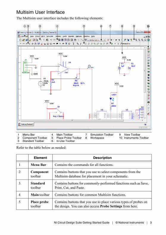
Multisim User Interface The Multisim user interface includes the following elements:
Refer to the table below as needed:
1 Menu Bar2 Component Toolbar3 Standard Toolbar
4 Main Toolbar5 Place Probe Toolbar6 In-Use Toolbar
7 Simulation Toolbar8 Workspace
9 View Toolbar10 Instruments Toolbar
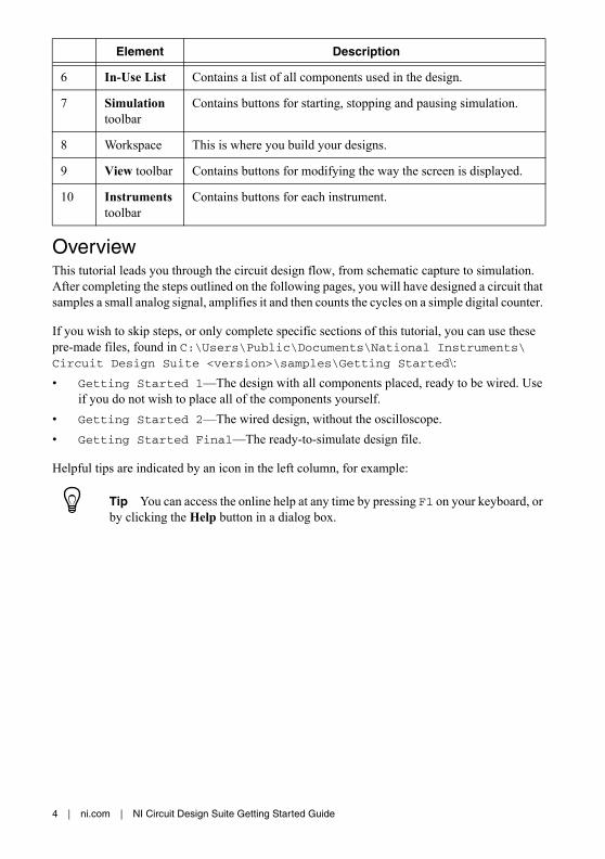
Element Description
1 Menu Bar Contains the commands for all functions.
2 Component toolbar
Contains buttons that you use to select components from the Multisim database for placement in your schematic.
3 Standard toolbar
Contains buttons for commonly-performed functions such as Save, Print, Cut, and Paste.
4 Main toolbar Contains buttons for common Multisim functions.
5 Place probe toolbar
Contains buttons that you use to place various types of probes on the design. You can also access Probe Settings from here.
4 | ni.com | NI Circuit Design Suite Getting Started Guide
Overview This tutorial leads you through the circuit design flow, from schematic capture to simulation. After completing the steps outlined on the following pages, you will have designed a circuit that samples a small analog signal, amplifies it and then counts the cycles on a simple digital counter.
If you wish to skip steps, or only complete specific sections of this tutorial, you can use these pre-made files, found in C:\Users\Public\Documents\National Instruments\Circuit Design Suite <version>\samples\Getting Started\:
• Getting Started 1—The design with all components placed, ready to be wired. Use if you do not wish to place all of the components yourself.
• Getting Started 2—The wired design, without the oscilloscope.
• Getting Started Final—The ready-to-simulate design file.
Helpful tips are indicated by an icon in the left column, for example:
Tip You can access the online help at any time by pressing F1 on your keyboard, or by clicking the Help button in a dialog box.
6 In-Use List Contains a list of all components used in the design.
7 Simulation toolbar
Contains buttons for starting, stopping and pausing simulation.
8 Workspace This is where you build your designs.
9 View toolbar Contains buttons for modifying the way the screen is displayed.
10 Instruments toolbar
Contains buttons for each instrument.
Element Description
NI Circuit Design Suite Getting Started Guide | © National Instruments | 5
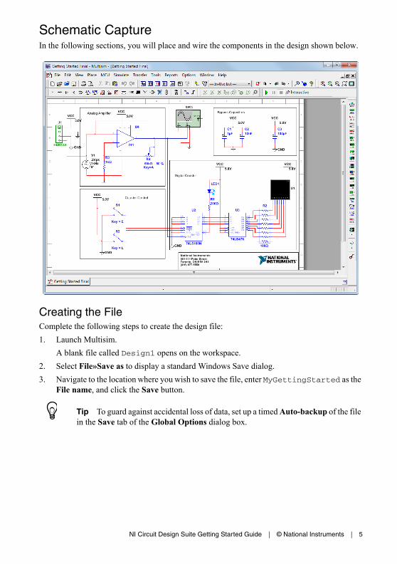
Schematic Capture In the following sections, you will place and wire the components in the design shown below.
Creating the File Complete the following steps to create the design file:
1. Launch Multisim.
A blank file called Design1 opens on the workspace.
2. Select File»Save as to display a standard Windows Save dialog.
3. Navigate to the location where you wish to save the file, enter MyGettingStarted as the File name, and click the Save button.
Tip To guard against accidental loss of data, set up a timed Auto-backup of the file in the Save tab of the Global Options dialog box.
6 | ni.com | NI Circuit Design Suite Getting Started Guide
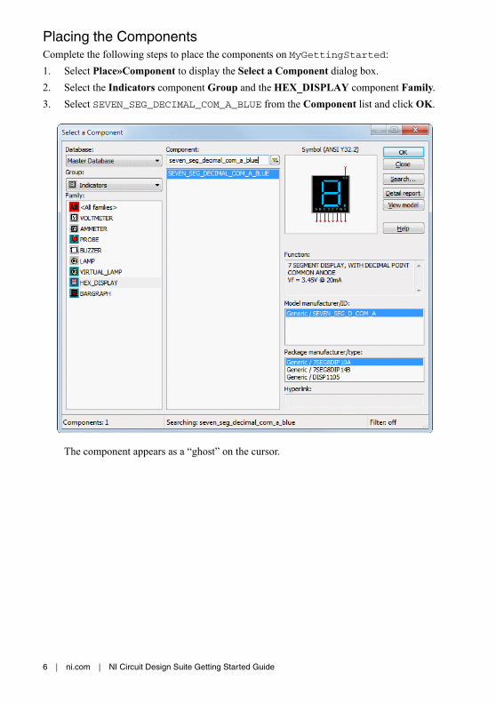
Placing the Components Complete the following steps to place the components on MyGettingStarted:
1. Select Place»Component to display the Select a Component dialog box.
2. Select the Indicators component Group and the HEX_DISPLAY component Family.
3. Select SEVEN_SEG_DECIMAL_COM_A_BLUE from the Component list and click OK.
The component appears as a “ghost” on the cursor.
NI Circuit Design Suite Getting Started Guide | © National Instruments | 7
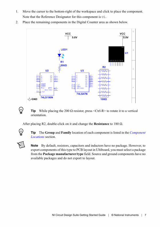
1. Move the cursor to the bottom-right of the workspace and click to place the component.
Note that the Reference Designator for this component is U1.
2. Place the remaining components in the Digital Counter area as shown below.
Tip While placing the 200 Ω resistor, press <Ctrl-R> to rotate it to a vertical orientation.
After placing R2, double-click on it and change the Resistance to 180 Ω.
Tip The Group and Family location of each component is listed in the Component Locations section.
Note By default, resistors, capacitors and inductors have no package. However, to export components of this type to PCB layout in Ultiboard, you must select a package from the Package manufacturer/type field. Source and ground components have no available packages and do not export to layout.
8 | ni.com | NI Circuit Design Suite Getting Started Guide
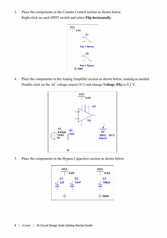
3. Place the components in the Counter Control section as shown below.
Right-click on each SPDT switch and select Flip horizontally.
4. Place the components in the Analog Amplifier section as shown below, rotating as needed.
Double-click on the AC voltage source (V1) and change Voltage (Pk) to 0.2 V.
5. Place the components in the Bypass Capacitors section as shown below.
NI Circuit Design Suite Getting Started Guide | © National Instruments | 9
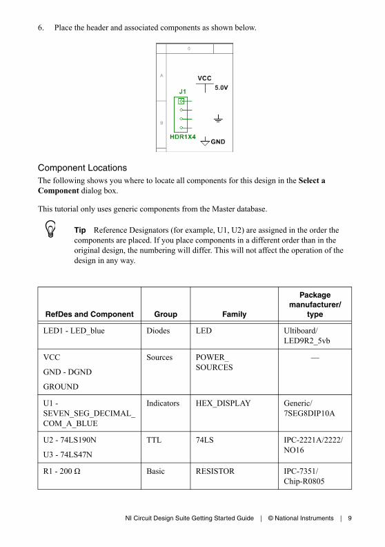
6. Place the header and associated components as shown below.
Component Locations The following shows you where to locate all components for this design in the Select a Component dialog box.
This tutorial only uses generic components from the Master database.
Tip Reference Designators (for example, U1, U2) are assigned in the order the components are placed. If you place components in a different order than in the original design, the numbering will differ. This will not affect the operation of the design in any way.
RefDes and Component Group Family
Package manufacturer/
type
LED1 - LED_blue Diodes LED Ultiboard/ LED9R2_5vb
VCC
GND - DGND
GROUND
Sources POWER_SOURCES
—
U1 - SEVEN_SEG_DECIMAL_COM_A_BLUE
Indicators HEX_DISPLAY Generic/ 7SEG8DIP10A
U2 - 74LS190N
U3 - 74LS47N
TTL 74LS IPC-2221A/2222/NO16
R1 - 200 Ω Basic RESISTOR IPC-7351/ Chip-R0805
10 | ni.com | NI Circuit Design Suite Getting Started Guide
Note When placing resistors, inductors, or capacitors, the Select a Component dialog box has slightly different fields than for other components. When placing these, you can choose any combination of the component’s value (for example, the resistance value), type (for example, carbon film), and so on. If you are placing a component that will be exported to PCB layout, the combination of values that you select must be available in a commercially available component.
Wiring the Design All components have pins that you use to wire them to other components or instruments. As soon as your cursor is over a pin, the cursor changes to a crosshair, indicating you can start wiring.
Tip You can wire the design that you placed on the workspace or you can use Getting Started 1 found in C:\Users\Public\Documents\National Instruments\Circuit Design Suite <version>\samples\Getting Started\.
Complete the following steps to wire the design:
1. Click on a pin on a component to start the connection (your cursor turns into a crosshair) and move the mouse.
A wire appears, attached to your cursor.
R2 - 8Line_Isolated Basic RPACK IPC-2221A/2222/ DIP-16
R3 - 1k Basic RESISTOR IPC-7351/ Chip-R0805
R4 - 50k Basic POTENTIOMETER Generic/ LIN_POT
S1, S2 - SPDT Basic SWITCH Generic/SPDT
U4 - 741 Analog OPAMP IPC-2221A/2222/ DIP-8
V1 - AC_VOLTAGE Sources SIGNAL_VOLTAGE_SOURCES
—
C1 - 1 μF
C2 - 10 nF
C3 - 100 μF
Basic CAP_ELECTROLIT IPC-7351/ Chip-C1210
J1 - HDR1X4 Connectors HEADERS_TEST Generic/ HDR1X4
RefDes and Component Group Family
Package manufacturer/
type
NI Circuit Design Suite Getting Started Guide | © National Instruments | 11
2. Click on a pin on the second component to finish the connection.
Multisim automatically places the wire, which snaps to an appropriate configuration, as shown below.
Tip You can also control the flow of the wire by clicking on points as you move the mouse. Each click “fixes” the wire to that point.
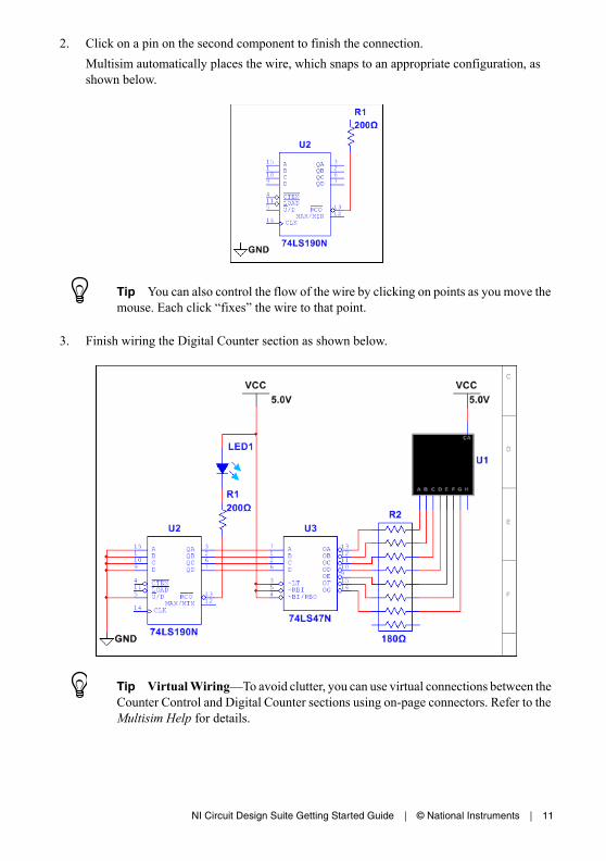
3. Finish wiring the Digital Counter section as shown below.
Tip Virtual Wiring—To avoid clutter, you can use virtual connections between the Counter Control and Digital Counter sections using on-page connectors. Refer to the Multisim Help for details.
12 | ni.com | NI Circuit Design Suite Getting Started Guide
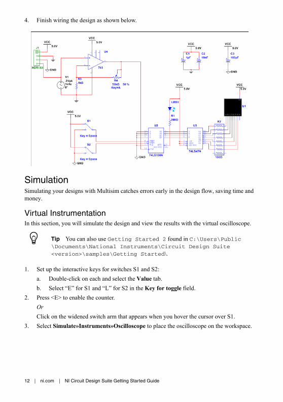
4. Finish wiring the design as shown below.
Simulation Simulating your designs with Multisim catches errors early in the design flow, saving time and money.
Virtual Instrumentation In this section, you will simulate the design and view the results with the virtual oscilloscope.
Tip You can also use Getting Started 2 found in C:\Users\Public\Documents\National Instruments\Circuit Design Suite <version>\samples\Getting Started\.
1. Set up the interactive keys for switches S1 and S2:
a. Double-click on each and select the Value tab.
b. Select “E” for S1 and “L” for S2 in the Key for toggle field.
2. Press <E> to enable the counter.
Or
Click on the widened switch arm that appears when you hover the cursor over S1.
3. Select Simulate»Instruments»Oscilloscope to place the oscilloscope on the workspace.
NI Circuit Design Suite Getting Started Guide | © National Instruments | 13
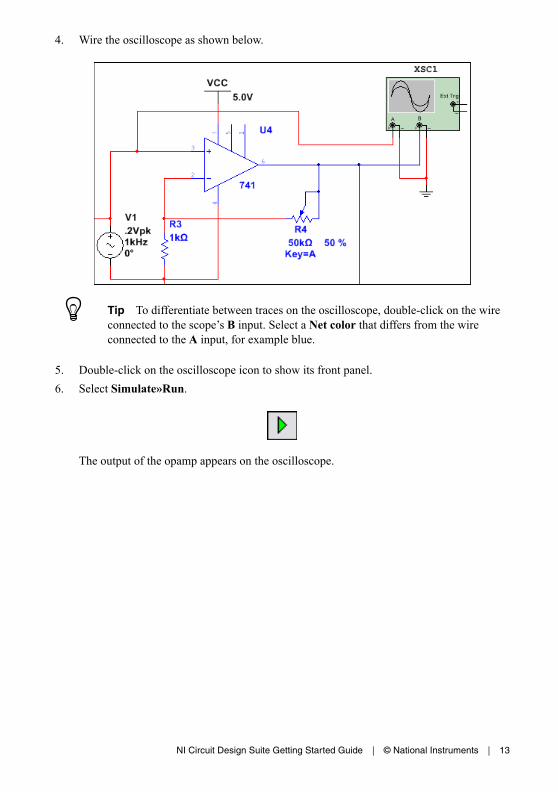
4. Wire the oscilloscope as shown below.
Tip To differentiate between traces on the oscilloscope, double-click on the wire connected to the scope’s B input. Select a Net color that differs from the wire connected to the A input, for example blue.
5. Double-click on the oscilloscope icon to show its front panel.
6. Select Simulate»Run.
The output of the opamp appears on the oscilloscope.
14 | ni.com | NI Circuit Design Suite Getting Started Guide
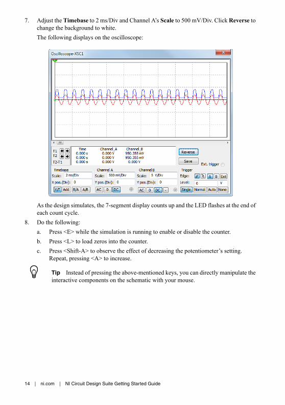
7. Adjust the Timebase to 2 ms/Div and Channel A’s Scale to 500 mV/Div. Click Reverse to change the background to white.
The following displays on the oscilloscope:
As the design simulates, the 7-segment display counts up and the LED flashes at the end of each count cycle.
8. Do the following:
a. Press <E> while the simulation is running to enable or disable the counter.
b. Press <L> to load zeros into the counter.
c. Press <Shift-A> to observe the effect of decreasing the potentiometer’s setting. Repeat, pressing <A> to increase.
Tip Instead of pressing the above-mentioned keys, you can directly manipulate the interactive components on the schematic with your mouse.
NI Circuit Design Suite Getting Started Guide | © National Instruments | 15
Analysis In this section, you will use AC Sweep to verify the frequency response of the amplifier.
Complete the following steps to perform an AC Sweep at the output of the op-amp:
1. Open Getting Started Final found in C:\Users\Public\Documents\National Instruments\Circuit Design Suite <version>\samples\Getting Started\.
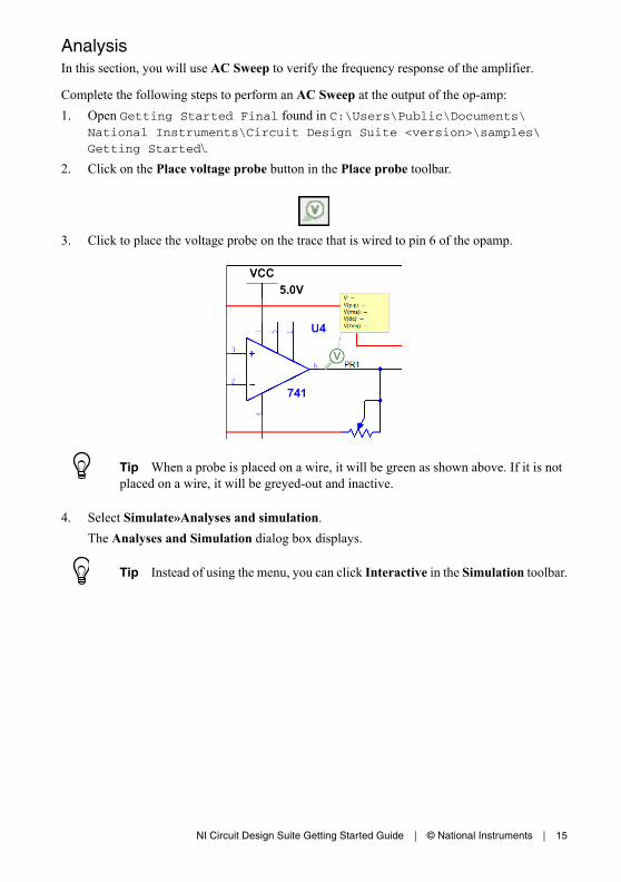
2. Click on the Place voltage probe button in the Place probe toolbar.
3. Click to place the voltage probe on the trace that is wired to pin 6 of the opamp.
Tip When a probe is placed on a wire, it will be green as shown above. If it is not placed on a wire, it will be greyed-out and inactive.
4. Select Simulate»Analyses and simulation.
The Analyses and Simulation dialog box displays.
Tip Instead of using the menu, you can click Interactive in the Simulation toolbar.
16 | ni.com | NI Circuit Design Suite Getting Started Guide
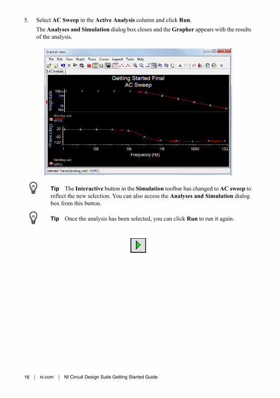
5. Select AC Sweep in the Active Analysis column and click Run.
The Analyses and Simulation dialog box closes and the Grapher appears with the results of the analysis.
Tip The Interactive button in the Simulation toolbar has changed to AC sweep to reflect the new selection. You can also access the Analyses and Simulation dialog box from this button.
Tip Once the analysis has been selected, you can click Run to run it again.
NI Circuit Design Suite Getting Started Guide | © National Instruments | 17
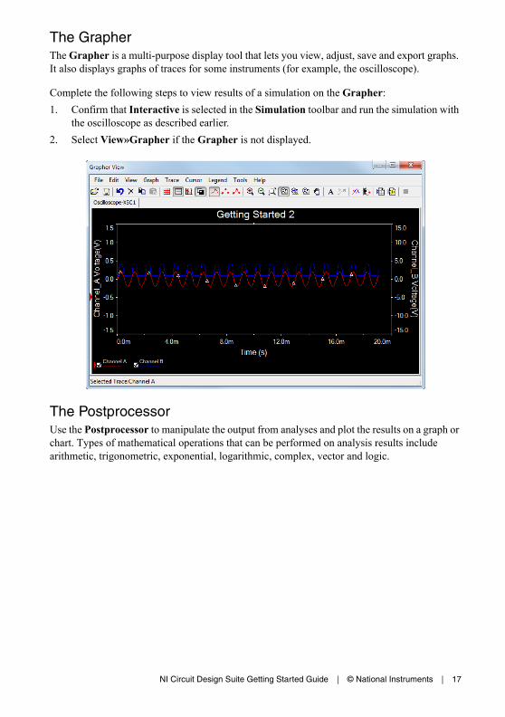
The Grapher The Grapher is a multi-purpose display tool that lets you view, adjust, save and export graphs. It also displays graphs of traces for some instruments (for example, the oscilloscope).
Complete the following steps to view results of a simulation on the Grapher:
1. Confirm that Interactive is selected in the Simulation toolbar and run the simulation with the oscilloscope as described earlier.
2. Select View»Grapher if the Grapher is not displayed.
The Postprocessor Use the Postprocessor to manipulate the output from analyses and plot the results on a graph or chart. Types of mathematical operations that can be performed on analysis results include arithmetic, trigonometric, exponential, logarithmic, complex, vector and logic.
18 | ni.com | NI Circuit Design Suite Getting Started Guide
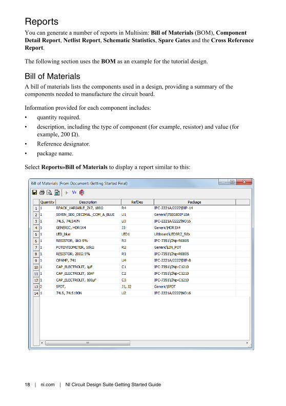
Reports You can generate a number of reports in Multisim: Bill of Materials (BOM), Component Detail Report, Netlist Report, Schematic Statistics, Spare Gates and the Cross Reference Report.
The following section uses the BOM as an example for the tutorial design.
Bill of Materials A bill of materials lists the components used in a design, providing a summary of the components needed to manufacture the circuit board.
Information provided for each component includes:
• quantity required.
• description, including the type of component (for example, resistor) and value (for example, 200 Ω).
• Reference designator.
• package name.
Select Reports»Bill of Materials to display a report similar to this:
NI Circuit Design Suite Getting Started Guide | © National Instruments | 19
Ultiboard TutorialThe tutorial in this section places the parts and traces for the circuit described in the Multisim Tutorial section.
Introduction to the Ultiboard Interface Ultiboard is the PCB layout application of Circuit Design Suite, a suite of EDA (Electronics Design Automation) tools that assists you in carrying out the major steps in the design flow.
Ultiboard is used to lay out and route printed circuit boards, perform certain basic mechanical CAD operations, and prepare boards for manufacturing. It also provides automated parts placement and wire routing.
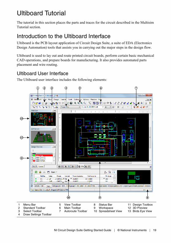
Ultiboard User Interface The Ultiboard user interface includes the following elements:
1 Menu Bar2 Standard Toolbar3 Select Toolbar4 Draw Settings Toolbar
5 View Toolbar6 Main Toolbar7 Autoroute Toolbar
8 Status Bar9 Workspace10 Spreadsheet View
11 Design Toolbox12 3D Preview13 Birds Eye View
20 | ni.com | NI Circuit Design Suite Getting Started Guide
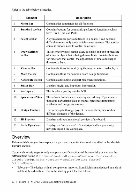
Refer to the table below as needed:
Overview This tutorial shows you how to place the parts and traces for the circuit described in the Multisim Tutorial section.
If you wish to skip steps, or only complete specific sections of this tutorial, you can use the different tabs, found in C:\Users\Public\Documents\National Instruments\Circuit Design Suite <version>\samples\Getting Started\GettingStarted:
• Tab GS1—The design with all components imported from Multisim and placed outside of a default board outline. This is the starting point for this tutorial.
Element Description
1 Menu Bar Contains the commands for all functions.
2 Standard toolbar Contains buttons for commonly-performed functions such as Save, Print, Cut, and Paste.
3 Select toolbar As you add more parts and traces to a board, it can become difficult to select only those which you want to use. This toolbar contains buttons used to control selections.
4 Draw Settings toolbar
This is where you select the layer, thickness and unit of measure of a line or object that is being drawn. It also contains buttons for functions that control the appearance of lines and shapes drawn on a layer.
5 View toolbar Contains buttons for modifying the way the screen is displayed.
6 Main toolbar Contains buttons for common board design functions.
7 Autoroute toolbar Contains autorouting and part placement functions.
8 Status Bar Displays useful and important information.
9 Workspace This is where you lay out the PCB.
10 Spreadsheet View This allows fast advanced viewing and editing of parameters including part details such as shapes, reference designators, attributes and design constraints.
11 Design Toolbox Use to navigate through project files and show, hide or dim different elements of the design.
12 3D Preview Displays a three-dimensional preview of the board.
13 Birds Eye View Displays an “aerial view” of the design and lets you easily navigate around the workspace.
NI Circuit Design Suite Getting Started Guide | © National Instruments | 21
• Tab GS2—The design with the imported components placed on the correctly sized board.
• Tab GS3—The design with the imported components placed on the board, and four holes placed from the database.
• Tab GS4—The design with all of the parts placed, and all of the copper (traces) routed.
• Tab GS5—The design with some parts placed and locked. Locked parts are not moved during autoplacement.
Helpful tips are indicated by an icon in the left column, for example:
Tip You can access the online help at any time by pressing F1 on your keyboard, or by clicking the Help button in a dialog box.
Opening the Tutorial Complete the following steps to open the tutorial file:
1. Launch Ultiboard, select File»Open samples and double-click on the Getting Started folder to open it.
2. Select GettingStarted and click Open.
The project file is loaded into Ultiboard.
Tip For instructions on transferring a design from Multisim to Ultiboard, refer to the Multisim Help and the Ultiboard Help.
22 | ni.com | NI Circuit Design Suite Getting Started Guide
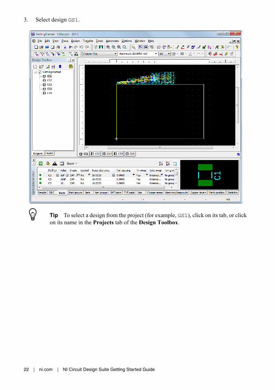
3. Select design GS1.
Tip To select a design from the project (for example, GS1), click on its tab, or click on its name in the Projects tab of the Design Toolbox.
NI Circuit Design Suite Getting Started Guide | © National Instruments | 23
Creating a Board Outline There is a default board outline, however, you can create one that is a more suitable size for the parts in this design in one of the following ways:
• Draw a board outline using the drawing tools.
• Import a DXF file.
• Use the Board Wizard.
Complete the following steps to experiment with the Board Wizard:
1. Double-click on Board Outline in the Layers tab to make it the active layer.
2. Click on the existing board outline in the GS1 design and press Delete on the keyboard.
3. Choose Tools»Board wizard.
4. Select Change the layer technology to make the Technology options available.
5. Select Multi-layers constructed with double-sided boards (layer pairs), and click Next. 6. Change the number of Layer pairs to 2 and leave Blind vias unchecked.
7. Click Next. In the Board Wizard - Shape of Board dialog box:
a. Confirm that Units is set to mil. b. Confirm that the Reference point is set to Bottom-left for Alignment. c. Confirm that the Rectangular option is selected in Board shape and size.
d. Set the Width to 3000 and the Height to 2000.
e. Set the Clearance to 5.00000.
This is the distance from the edge of the board that is to be kept free of parts or any other elements.
8. Click Finish.
The board outline is placed on your design.
Note For complete details on the Board Wizard, refer to the Ultiboard Help.
Complete the following to move the board outline:
1. Click anywhere on the board outline in the workspace and drag the board to a location just below the row of parts.
Complete the following steps to change the reference point:
1. Select Design»Set reference point. The reference point is attached to your cursor.
24 | ni.com | NI Circuit Design Suite Getting Started Guide
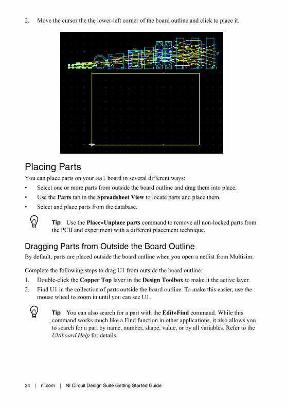
2. Move the cursor the the lower-left corner of the board outline and click to place it.
Placing Parts You can place parts on your GS1 board in several different ways:
• Select one or more parts from outside the board outline and drag them into place.
• Use the Parts tab in the Spreadsheet View to locate parts and place them.
• Select and place parts from the database.
Tip Use the Place»Unplace parts command to remove all non-locked parts from the PCB and experiment with a different placement technique.
Dragging Parts from Outside the Board Outline By default, parts are placed outside the board outline when you open a netlist from Multisim.
Complete the following steps to drag U1 from outside the board outline:
1. Double-click the Copper Top layer in the Design Toolbox to make it the active layer.
2. Find U1 in the collection of parts outside the board outline. To make this easier, use the mouse wheel to zoom in until you can see U1.
Tip You can also search for a part with the Edit»Find command. While this command works much like a Find function in other applications, it also allows you to search for a part by name, number, shape, value, or by all variables. Refer to the Ultiboard Help for details.
NI Circuit Design Suite Getting Started Guide | © National Instruments | 25
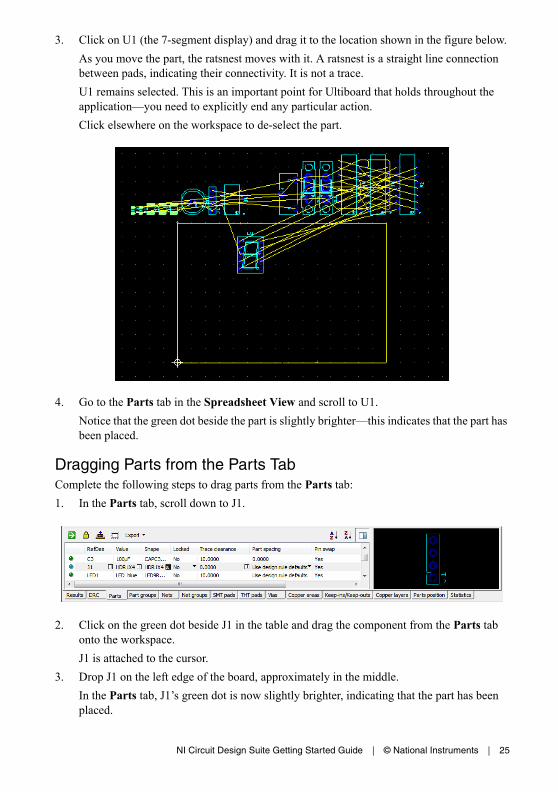
3. Click on U1 (the 7-segment display) and drag it to the location shown in the figure below.
As you move the part, the ratsnest moves with it. A ratsnest is a straight line connection between pads, indicating their connectivity. It is not a trace.
U1 remains selected. This is an important point for Ultiboard that holds throughout the application—you need to explicitly end any particular action.
Click elsewhere on the workspace to de-select the part.
4. Go to the Parts tab in the Spreadsheet View and scroll to U1.
Notice that the green dot beside the part is slightly brighter—this indicates that the part has been placed.
Dragging Parts from the Parts Tab Complete the following steps to drag parts from the Parts tab:
1. In the Parts tab, scroll down to J1.
2. Click on the green dot beside J1 in the table and drag the component from the Parts tab onto the workspace.
J1 is attached to the cursor.
3. Drop J1 on the left edge of the board, approximately in the middle.
In the Parts tab, J1’s green dot is now slightly brighter, indicating that the part has been placed.
26 | ni.com | NI Circuit Design Suite Getting Started Guide
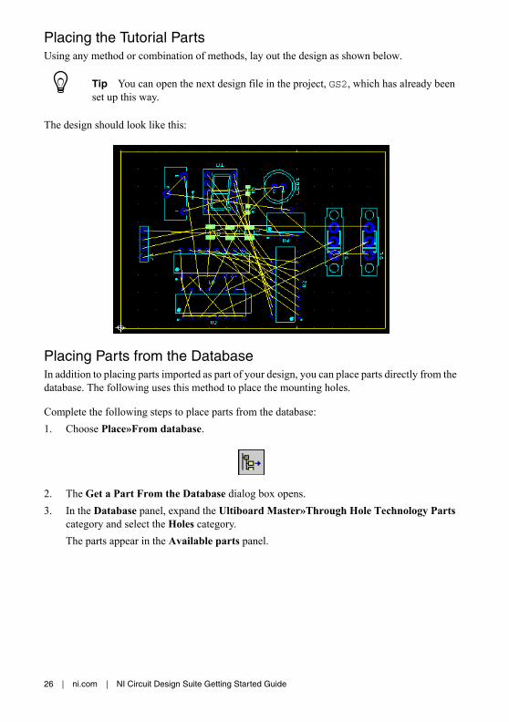
Placing the Tutorial PartsUsing any method or combination of methods, lay out the design as shown below.
Tip You can open the next design file in the project, GS2, which has already been set up this way.
The design should look like this:
Placing Parts from the Database In addition to placing parts imported as part of your design, you can place parts directly from the database. The following uses this method to place the mounting holes.
Complete the following steps to place parts from the database:
1. Choose Place»From database.
2. The Get a Part From the Database dialog box opens.
3. In the Database panel, expand the Ultiboard Master»Through Hole Technology Parts category and select the Holes category.
The parts appear in the Available parts panel.
NI Circuit Design Suite Getting Started Guide | © National Instruments | 27
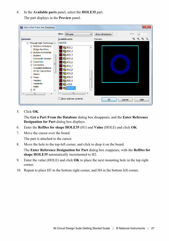
4. In the Available parts panel, select the HOLE35 part.
The part displays in the Preview panel.
5. Click OK.
The Get a Part From the Database dialog box disappears, and the Enter Reference Designation for Part dialog box displays.
6. Enter the RefDes for shape HOLE35 (H1) and Value (HOLE) and click OK.
7. Move the cursor over the board.
The part is attached to the cursor.
8. Move the hole to the top-left corner, and click to drop it on the board.
The Enter Reference Designation for Part dialog box reappears, with the RefDes for shape HOLE35 automatically incremented to H2.
9. Enter the value (HOLE) and click OK to place the next mounting hole in the top right corner.
10. Repeat to place H3 in the bottom right corner, and H4 in the bottom left corner.
28 | ni.com | NI Circuit Design Suite Getting Started Guide
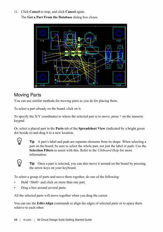
11. Click Cancel to stop, and click Cancel again.
The Get a Part From the Database dialog box closes.
Moving PartsYou can use similar methods for moving parts as you do for placing them.
To select a part already on the board, click on it.
To specify the X/Y coordinates to where the selected part is to move, press * on the numeric keypad.
Or, select a placed part in the Parts tab of the Spreadsheet View (indicated by a bright green dot beside it) and drag it to a new location.
Tip A part’s label and pads are separate elements from its shape. When selecting a part on the board, be sure to select the whole part, not just the label or pads. Use the Selection Filters to assist with this. Refer to the Ultiboard Help for more information.
Tip Once a part is selected, you can also move it around on the board by pressing the arrow keys on your keyboard.
To select a group of parts and move them together, do one of the following:
• Hold <Shift> and click on more than one part.
• Drag a box around several parts.
All the selected parts will move together when you drag the cursor.
You can use the Edit»Align commands to align the edges of selected parts or to space them relative to each other.
NI Circuit Design Suite Getting Started Guide | © National Instruments | 29
Use the Edit»Align commands to align the mounting holes you just placed:
1. Select H1 and hold <Shift> to select H2.
2. Choose Edit»Align»Align top.
If H2 was not originally placed exactly in line with H1, you will see it move.
3. Click on an empty space on the board to clear the selection, then select H2 and H3.
4. Choose Edit»Align»Align right. 5. Continue in this manner to align the bottoms of H3 and H4, and the left sides of H1 and H4.
Placing Traces You have the following options for placing traces:
• Manual trace.
• Follow-me trace.
• Connection machine trace.
A manual trace is placed exactly as you specify, even running through a component or trace if that is the path you set.
A follow-me trace automatically draws a valid trace between the pins you select with your mouse movements—you can move from pin to pin, leaving a valid trace.
A connection machine trace automatically joins two pins by the most efficient route, though you have the option of changing it.
As you place a trace, and before you click to fix it in place, you can remove a segment by backing up over it.
Each time you click while placing a manual trace, or each time a follow-me trace or connection machine trace changes direction, a separate segment of that trace is created.
Tip When performing operations on traces, be sure to select either the appropriate segment or the whole trace.
Placing a Manual Trace You can continue with the design you have been working on, or open GS3.
Be sure you are on the Copper Top layer before beginning—Copper Top must be highlighted in red in the Layers tab of the Design Toolbox.
Complete the following steps to place a trace manually:
1. Choose Place»Line.
Tip The Line command creates a line on any layer. The results differ depending on the layer selected. For example, if the selected layer is silkscreen, a line is created on the silkscreen layer of the PCB. If the selected layer is a copper layer, then the line is actually a trace.
30 | ni.com | NI Circuit Design Suite Getting Started Guide
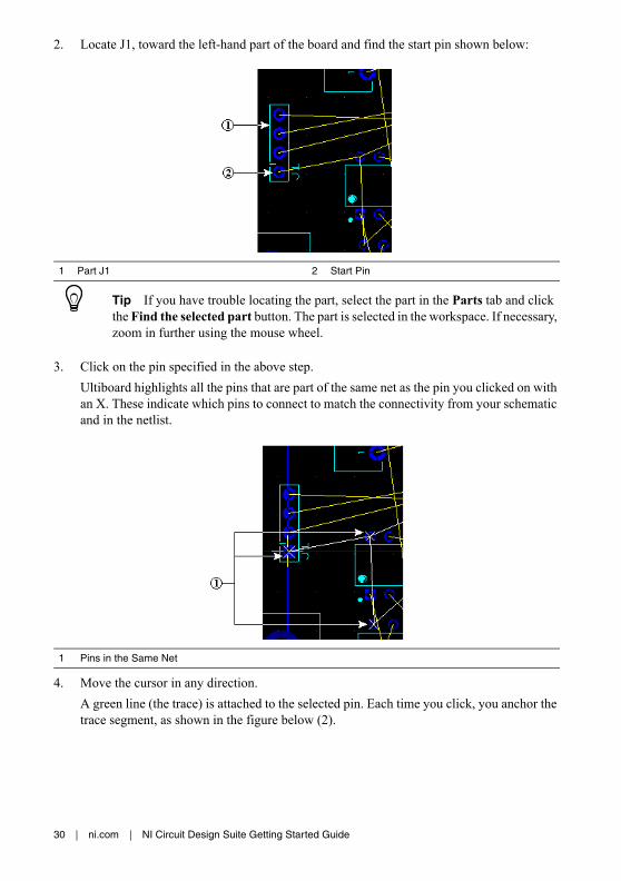
2. Locate J1, toward the left-hand part of the board and find the start pin shown below:
Tip If you have trouble locating the part, select the part in the Parts tab and click the Find the selected part button. The part is selected in the workspace. If necessary, zoom in further using the mouse wheel.
3. Click on the pin specified in the above step.
Ultiboard highlights all the pins that are part of the same net as the pin you clicked on with an X. These indicate which pins to connect to match the connectivity from your schematic and in the netlist.
4. Move the cursor in any direction.
A green line (the trace) is attached to the selected pin. Each time you click, you anchor the trace segment, as shown in the figure below (2).
1 Part J1 2 Start Pin
1 Pins in the Same Net
NI Circuit Design Suite Getting Started Guide | © National Instruments | 31
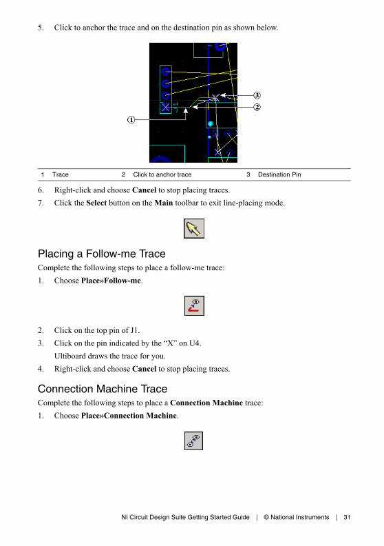
5. Click to anchor the trace and on the destination pin as shown below.
6. Right-click and choose Cancel to stop placing traces.
7. Click the Select button on the Main toolbar to exit line-placing mode.
Placing a Follow-me Trace Complete the following steps to place a follow-me trace:
1. Choose Place»Follow-me.
2. Click on the top pin of J1.
3. Click on the pin indicated by the “X” on U4.
Ultiboard draws the trace for you.
4. Right-click and choose Cancel to stop placing traces.
Connection Machine Trace Complete the following steps to place a Connection Machine trace:
1. Choose Place»Connection Machine.
1 Trace 2 Click to anchor trace 3 Destination Pin
32 | ni.com | NI Circuit Design Suite Getting Started Guide
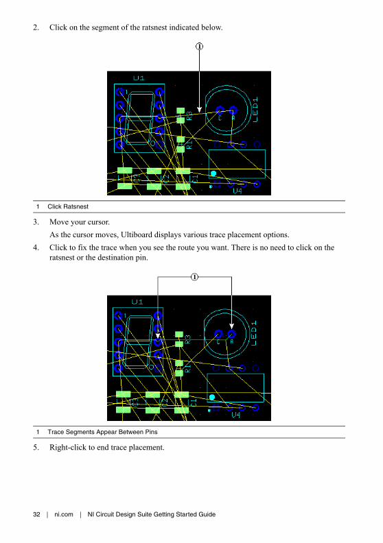
2. Click on the segment of the ratsnest indicated below.
3. Move your cursor.
As the cursor moves, Ultiboard displays various trace placement options.
4. Click to fix the trace when you see the route you want. There is no need to click on the ratsnest or the destination pin.
5. Right-click to end trace placement.
1 Click Ratsnest
1 Trace Segments Appear Between Pins
NI Circuit Design Suite Getting Started Guide | © National Instruments | 33
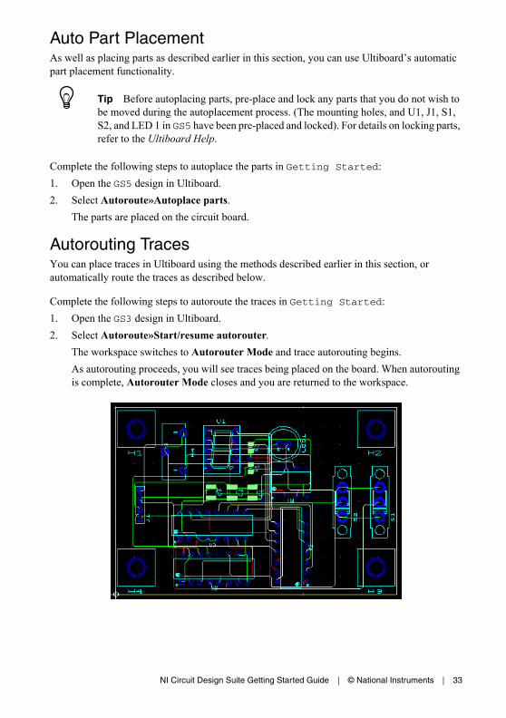
Auto Part Placement As well as placing parts as described earlier in this section, you can use Ultiboard’s automatic part placement functionality.
Tip Before autoplacing parts, pre-place and lock any parts that you do not wish to be moved during the autoplacement process. (The mounting holes, and U1, J1, S1, S2, and LED 1 in GS5 have been pre-placed and locked). For details on locking parts, refer to the Ultiboard Help.
Complete the following steps to autoplace the parts in Getting Started:
1. Open the GS5 design in Ultiboard.
2. Select Autoroute»Autoplace parts.
The parts are placed on the circuit board.
Autorouting Traces You can place traces in Ultiboard using the methods described earlier in this section, or automatically route the traces as described below.
Complete the following steps to autoroute the traces in Getting Started:
1. Open the GS3 design in Ultiboard.
2. Select Autoroute»Start/resume autorouter.
The workspace switches to Autorouter Mode and trace autorouting begins.
As autorouting proceeds, you will see traces being placed on the board. When autorouting is complete, Autorouter Mode closes and you are returned to the workspace.
34 | ni.com | NI Circuit Design Suite Getting Started Guide
The autorouter can be stopped at any time and you can make manual changes as desired. When you restart the autorouter, it will continue with the changes you made. Remember to lock any traces that you have placed manually and do not wish to be moved by the autorouter.
Tip Use the Routing Options dialog box to modify autoplacement and autorouting options. Refer to the Ultiboard Help for details.
Preparing for Manufacturing/Assembly Ultiboard can produce many different output formats to support your production and manufacturing needs. The following sections explain the functions performed to output your board for production and documentation purposes.
Cleaning up the Board Before sending the board for manufacturing, you should clean up any open trace ends (trace segments that do not have any terminating connections in the design) and unused vias.
To delete any open trace ends, open the GS4 design and choose Edit»Copper delete»Open trace ends.
To delete any unused vias, select Design»Remove unused vias. This deletes all vias that do not have any trace segments or copper areas connected to them.
Adding Comments Comments can be used to show engineering change orders, to facilitate collaborative work among team members, or to allow background information to be attached to a design.
You can pin a comment to the workspace, or directly to a part. When a part with an attached comment is moved, the comment also moves.
Refer to the Ultiboard Help for details.
Exporting a File You can export a number of file types, including Gerber. An exported file contains complete information describing how a finished board is to be manufactured.
Refer to the Ultiboard Help for details.
NI Circuit Design Suite Getting Started Guide | © National Instruments | 35
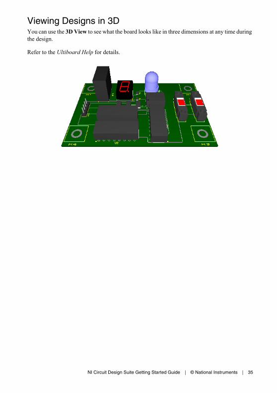
Viewing Designs in 3D You can use the 3D View to see what the board looks like in three dimensions at any time during the design.
Refer to the Ultiboard Help for details.

© 2006–2016 National Instruments. All rights reserved.
374482J-01 Feb16
Refer to the NI Trademarks and Logo Guidelines at ni.com/trademarks for more information on National Instruments trademarks. Other product and company names mentioned herein are trademarks or trade names of their respective companies. For patents covering National Instruments products/technology, refer to the appropriate location: Help»Patents in your software, the patents.txt file on your media, or the National Instruments Patents Notice at ni.com/patents. You can find information about end-user license agreements (EULAs) and third-party legal notices in the readme file for your NI product. Refer to the Export Compliance Information at ni.com/legal/export-compliance for the National Instruments global trade compliance policy and how to obtain relevant HTS codes, ECCNs, and other import/export data. NI MAKES NO EXPRESS OR IMPLIED WARRANTIES AS TO THE ACCURACY OF THE INFORMATION CONTAINED HEREIN AND SHALL NOT BE LIABLE FOR ANY ERRORS. U.S. Government Customers: The data contained in this manual was developed at private expense and is subject to the applicable limited rights and restricted data rights as set forth in FAR 52.227-14, DFAR 252.227-7014, and DFAR 252.227-7015.