Embed Size (px)
Citation preview
July 2016 DocID029535 Rev 1 1/14
www.st.com
UM2088 User manual
Getting started with the 2 kW fully digital AC-DC power supply (D-SMPS) evaluation board
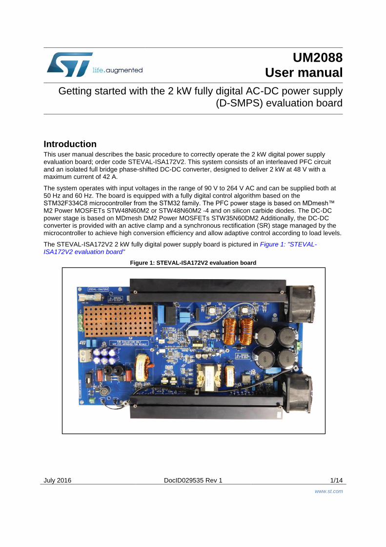
Introduction This user manual describes the basic procedure to correctly operate the 2 kW digital power supply evaluation board; order code STEVAL-ISA172V2. This system consists of an interleaved PFC circuit and an isolated full bridge phase-shifted DC-DC converter, designed to deliver 2 kW at 48 V with a maximum current of 42 A.
The system operates with input voltages in the range of 90 V to 264 V AC and can be supplied both at 50 Hz and 60 Hz. The board is equipped with a fully digital control algorithm based on the STM32F334C8 microcontroller from the STM32 family. The PFC power stage is based on MDmesh™ M2 Power MOSFETs STW48N60M2 or STW48N60M2 -4 and on silicon carbide diodes. The DC-DC power stage is based on MDmesh DM2 Power MOSFETs STW35N60DM2 Additionally, the DC-DC converter is provided with an active clamp and a synchronous rectification (SR) stage managed by the microcontroller to achieve high conversion efficiency and allow adaptive control according to load levels.
The STEVAL-ISA172V2 2 kW fully digital power supply board is pictured in Figure 1: "STEVAL-ISA172V2 evaluation board"
Figure 1: STEVAL-ISA172V2 evaluation board

Contents UM2088
2/14 DocID029535 Rev 1
Contents
1 Safety and operating instructions .................................................. 5
2 Evaluation board overview ............................................................. 6
3 Operating the board ...................................................................... 11
4 Revision history ............................................................................ 13

UM2088 List of tables
DocID029535 Rev 1 3/14
List of tables
Table 1: 2 kW AC-DC fully digital power supply specifications .................................................................. 9 Table 2: Document revision history .......................................................................................................... 13

List of figures UM2088
4/14 DocID029535 Rev 1
List of figures
Figure 1: STEVAL-ISA172V2 evaluation board .......................................................................................... 1 Figure 2: STEVAL-ISA172V2 system architecture ..................................................................................... 6 Figure 3: Two-stage EMC filter ................................................................................................................... 7 Figure 4: PFC circuit section ....................................................................................................................... 7 Figure 5: DC-DC converter circuit section .................................................................................................. 8 Figure 6: Auxiliary power supply circuit ...................................................................................................... 9 Figure 7: AC cables and output load connection ...................................................................................... 11 Figure 8: Programming connector ............................................................................................................ 12

UM2088 Safety and operating instructions
DocID029535 Rev 1 5/14
1 Safety and operating instructions
General
During assembly and operation, the 2 kW D-SMPS power supply STEVAL-ISA172V2 poses several inherent hazards, including bare wires, moving or rotating parts for the presence of a fan, and hot surfaces. There is danger of serious personal injury and damage to property if the DC-DC converter or its components are improperly used or installed incorrectly.
All operations involving transportation, installation and use, as well as maintenance are to be carried out by skilled technical personnel (national accident prevention rules must be observed). For the purposes of these basic safety instructions, "skilled technical personnel" are suitably qualified people who are familiar with the installation, use and maintenance of power electronic systems.
2 kW D-SMPS power supply intended use
The technical data as well as information concerning the power supply conditions shall be taken from the documentation and strictly observed.
Electrical connection
The electrical installation shall be completed in accordance with the appropriate requirements (e.g., cross-sectional areas of conductors, fusing, GND connections).The board is intended only for evaluation purpose. Supply the STEVAL-ISA172V2 only with an AC source lab power supply.
Evaluation board operation
Do not touch the design boards immediately after disconnecting the voltage supply as several parts and power terminals may still have charged capacitors that need time to discharge.
Always use the 2 kW D-SMPS STEVAL-ISA172V2 with the plexiglas provided with the board.
Do not use the board without the aluminum plate installed under the PCB.
Evaluation board overview UM2088
6/14 DocID029535 Rev 1
2 Evaluation board overview
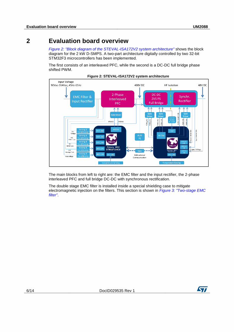
Figure 2: "Block diagram of the STEVAL-ISA172V2 system architecture" shows the block diagram for the 2 kW D-SMPS. A two-part architecture digitally controlled by two 32-bit STM32F3 microcontrollers has been implemented.
The first consists of an interleaved PFC, while the second is a DC-DC full bridge phase shifted PWM.
Figure 2: STEVAL-ISA172V2 system architecture
The main blocks from left to right are: the EMC filter and the input rectifier, the 2-phase interleaved PFC and full bridge DC-DC with synchronous rectification.
The double stage EMC filter is installed inside a special shielding case to mitigate electromagnetic injection on the filters. This section is shown in Figure 3: "Two-stage EMC filter".
UM2088 Evaluation board overview
DocID029535 Rev 1 7/14
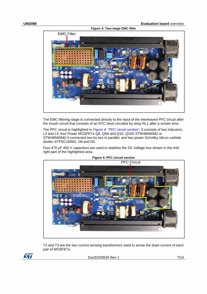
Figure 3: Two-stage EMC filter
The EMC filtering stage is connected directly to the input of the interleaved PFC circuit after the inrush circuit that consists of an NTC short circuited by relay RL1 after a certain time.
The PFC circuit is highlighted in Figure 4: "PFC circuit section". It consists of two inductors, L3 and L4, four Power MOSFETs Q9, Q9A and Q10, Q10A STW48N60M2 or STW48N60M2-4 connected two by two in parallel, and two power Schottky silicon carbide diodes STPSC1006D, D8 and D9.
Four 470 µF 450 V capacitors are used to stabilize the DC voltage bus shown in the mid-right part of the highlighted area.
Figure 4: PFC circuit section
T2 and T3 are the two current sensing transformers used to sense the drain current of each pair of MOSFETs.

Evaluation board overview UM2088
8/14 DocID029535 Rev 1
The DC-DC full bridge PWM phase shifted stage performs voltage step-down using an HF transformer with a primary-to-secondary turn ratio chosen to maintain good efficiency and regulation across the whole operating range. The transformer is supplied with a voltage whose average value depends on the phase shift of the primary side active switches. On the secondary side, this voltage waveform is rectified and then smoothed by the output filter. While on the primary side, switching losses are reduced thanks to zero voltage switching (ZVS); on the secondary side, synchronous rectification (SR) is used to ensure low conduction losses.
The DC-DC converter is highlighted in Figure 5: "DC-DC converter circuit section". This section consists of the four Power MOSFETs of the full-bridge Q1, Q2, Q3, Q4 STW35N60DM2, the high frequency transformer T4, the resonant inductor L6 and the synchronous rectifier MOSFETs Q11, Q12, Q13, Q14.
The output filter capacitors are shown in the left part of the highlighted area in Figure 5: "DC-DC converter circuit section".
The full-bridge DC-DC converter is driven by two PM8834, IC1 and IC2, through the pulse transformers TX1 and TX2, while the secondary side synchronous rectification is driven by a single PM8834 IC3.
Note the presence of the active clamp on the lower left side, consisting of the MDmesh DM2 Power MOSFETs STP24N60DM2, M1 and M2, and others passive components.
L11 and L12 are two pulse transformers to supply the gate signal of the active clamp switches together with a PM8834.The clamp PWM signals are generated by the microcontroller to cancel the peak voltage overshoot generated by energy stored in the leakage inductance of HF transformer.
Two dedicated opto-isolators, U7 and U8, are used for bidirectional serial communication between the PFC and DC-DC converter.
Figure 5: DC-DC converter circuit section
It is possible to program the two microcontrollers through connectors J5 and J8 for PFC and DC-DC converter respectively, using IAR Embedded Workbench for ARM ver. 6.50 or

UM2088 Evaluation board overview
DocID029535 Rev 1 9/14
higher and a suitable debugger/programmer such as IAR J-Link or STMicroelectronics ST-Link. The auxiliary power supply section implemented with a VIPER27HD circuit is highlighted in Figure 6: "Auxiliary power supply circuit".
Figure 6: Auxiliary power supply circuit
Table 1: "2 kW AC-DC fully digital power supply specifications" lists the main specifications of the 2 kW Fully Digital AC-DC power supply:
Table 1: 2 kW AC-DC fully digital power supply specifications
Parameter Value
Input AC voltage 90 V AC up to 264 V AC
Input AC frequency 45 Hz up to 65 Hz
Output voltage 48 V DC
Max output current 42 A
PFC output voltage 400 V DC
Output power 2000 W
PFC switching frequency 60 kHz
DC-DC switching frequency 100 kHz
HF transformer isolation 4 kV
Cooling Forced air with speed modulation
Input short-circuit protection 25 A fuse
Input under/overvoltage Managed by primary STM32F334C8
Input under/over-frequency Managed by primary STM32F334C8
Bus DC under/overvoltage Managed by primary STM32F334C8
Output under/overvoltage Managed by secondary STM32F334C8
Output short-circuit protection Managed by secondary STM32F334C8
Over-temperature protection Managed by both STM32F334C8s

Evaluation board overview UM2088
10/14 DocID029535 Rev 1
The 2 kW AC-DC converter accepts universal input voltage and produces a 48 V regulated output. The continuous power rating of the unit is 2 kW. Forced air cooling is used with air flow speed proportional to the output power. The ambient operating temperature range is from 0 °C to 50 °C. The intermediate high-voltage DC bus is regulated at 400 V by the PFC, which draws sinusoidal input current from the AC input, maintaining a high power factor and low current total harmonic distortion (THD%). The DC-DC circuit converts this high DC voltage to low DC voltage proving isolation (4 kV) by means of an HF transformer and high efficiency thanks to ZVS. Input and output current and voltage protection are also provided together with over-temperature protection.
UM2088 Operating the board
DocID029535 Rev 1 11/14
3 Operating the board
The AC-DC converter must be only used in a power laboratory. The high voltage used in any power systems presents a serious shock hazard. The board can be easily tested up to 2 kW and across the operating input voltage and frequency range. A list of equipment that can be used to perform functional and efficiency testing is provided below:
2.4 kVA programmable AC source
60 V / 45 A DC electronic load
Power analyzer
Digital oscilloscope
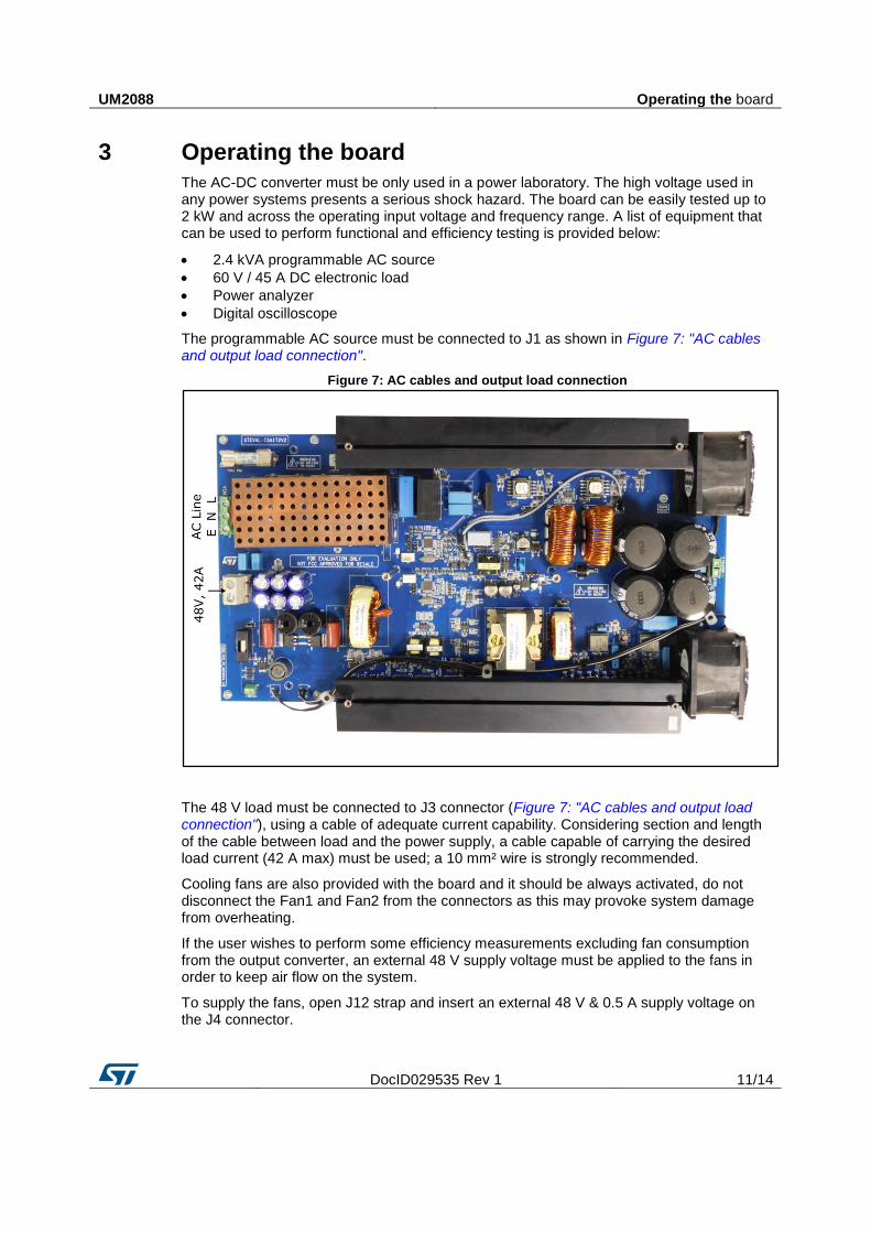
The programmable AC source must be connected to J1 as shown in Figure 7: "AC cables and output load connection".
Figure 7: AC cables and output load connection
The 48 V load must be connected to J3 connector (Figure 7: "AC cables and output load connection"), using a cable of adequate current capability. Considering section and length of the cable between load and the power supply, a cable capable of carrying the desired load current (42 A max) must be used; a 10 mm² wire is strongly recommended.
Cooling fans are also provided with the board and it should be always activated, do not disconnect the Fan1 and Fan2 from the connectors as this may provoke system damage from overheating.
If the user wishes to perform some efficiency measurements excluding fan consumption from the output converter, an external 48 V supply voltage must be applied to the fans in order to keep air flow on the system.
To supply the fans, open J12 strap and insert an external 48 V & 0.5 A supply voltage on the J4 connector.

Operating the board UM2088
12/14 DocID029535 Rev 1
Once the input power supply (90 V to 264 V AC, 45 Hz to 65 Hz) and output load (48 V, 0 A to 42 A) are connected, the power supply is ready to start.
As soon as the input voltage is above 80 V, the auxiliary power supply begins supplying the microcontrollers, drivers and signal conditioning circuitry. In this operating condition the PFC and DC-DC converter are in idle mode.
If the input voltage is within the proper range ([90 V, 264 V] and [40 Hz, 65 Hz]) PFC starts ramp-up procedure and charges DC bus at 400 V; LED D47 blinks until this start-up procedure completes, after which it remains on. Once the DC bus is charged, a serial message is sent from the PFC microcontroller U9 to the DC-DC converter microcontroller U11, which enables the modulation of the DC-DC switching and SR devices. The output voltage will ramp up from 0 V to 48 V with LED D55 blinking, after which the system reaches a steady state.
Reprogramming the board
If it is necessary to reprogram the board, the user has to make a proper programming cable to adapt a JTAG connector to the 4-pin programming connector placed in the board.
A female wire-to-board connector with a pitch of 2.5 mm (like the MOLEX 22-01-1042) must be used following the pinout shown in Figure 8: "Programming connector".
To program primary or secondary microcontroller, this programming cable must to be connected to J6 or J10 respectively. This operation should be done when the input voltage is disconnected or equal to zero.
Once the programming cable is connected between board's connector and the chosen programmer (like ST-Link or J-Link), the board can be supplied with 80V AC to assure that the auxiliary power supply is operating, but the PFC doesn't start to regulate the bus voltage.
After programming the board, the user should remove the input voltage and wait for the discharge of bus capacitors (green LEDs D46 and D54 must be off), before disconnecting the programming cable.
Figure 8: Programming connector
UM2088 Revision history
DocID029535 Rev 1 13/14
4 Revision history Table 2: Document revision history
Date Revision Changes
07-Jul-2016 1 Initial release.

UM2088
14/14 DocID029535 Rev 1
IMPORTANT NOTICE – PLEASE READ CAREFULLY
STMicroelectronics NV and its subsidiaries (“ST”) reserve the right to make changes, corrections, enhancements, modifications , and improvements to ST products and/or to this document at any time without notice. Purchasers should obtain the latest relevant information on ST products before placing orders. ST products are sold pursuant to ST’s terms and conditions of sale in place at the time of order acknowledgement.
Purchasers are solely responsible for the choice, selection, and use of ST products and ST assumes no liability for application assistance or the design of Purchasers’ products.
No license, express or implied, to any intellectual property right is granted by ST herein.
Resale of ST products with provisions different from the information set forth herein shall void any warranty granted by ST for such product.
ST and the ST logo are trademarks of ST. All other product or service names are the property of their respective owners.
Information in this document supersedes and replaces information previously supplied in any prior versions of this document.
© 2016 STMicroelectronics – All rights reserved