Embed Size (px)
Citation preview
Giant Discrete Steps in Metal-Insulator Transition in Perovskite Manganite Wires
Hong-Ying Zhai,1 J. X. Ma,1,3 D. T. Gillaspie,1,3 X. G. Zhang,2,4 T. Z. Ward,1,3 E. W. Plummer,1,2,3 and J. Shen1,2,3,*1Materials Science and Technology Division, Oak Ridge National Laboratory, Oak Ridge, Tennessee 37831, USA
2Center for Nanophase Materials Science Division, Oak Ridge National Laboratory, Oak Ridge, Tennessee 37831, USA3Department of Physics and Astronomy, The University of Tennessee, Knoxville, Tennessee 37996, USA
4Computer Science and Mathematics Division, Oak Ridge National Laboratory, Oak Ridge, Tennessee 37831, USA(Received 1 August 2006; published 17 October 2006)
Optical lithography is used to fabricate LPCMO wires starting from a single !La5=8"0:3Pr0:3#Ca3=8MnO3
(LPCMO) film epitaxially grown on a LaAlO3!100# substrate. As the width of the wires is decreased, theresistivity of the LPCMO wires exhibits giant and ultrasharp steps upon varying temperature and magneticfield in the vicinity of the metal-insulator transition. The origin of the ultrasharp transitions is attributed tothe effect of spatial confinement on the percolative transport in manganites.
DOI: 10.1103/PhysRevLett.97.167201 PACS numbers: 75.47.Lx, 71.30.+h, 75.30.Kz, 75.47.Gk
The strong spin-charge-lattice interaction in transitionmetal oxides (TMOs) often leads to a striking phenomenoncalled electronic phase separation (PS), which is identifiedwith the coexistence of a range of exotic electronic andmagnetic phases despite the single crystalline structure [1].The role of the PS in the related physical properties such ashigh-Tc superconducting and colossal magnetoresistance(CMR) is a hotly debated issue in the field of condensedmatter physics. Spatial confinement is a very useful routeto gain deeper insight into the nature of PS. In particular,when the spatial dimension of the TMOs is reduced to thecharacteristic PS length scale, one would expect thatchanges in the transport properties of the TMOs could bequite dramatic.
A model system for this study is La5=8"xPrxCa3=8MnO3
(LPCMO), a perovskite manganite that is famously knownfor its large-scale PS. Transmission electron microscopyhas revealed submicrometer-scaled ferromagnetic (FM)and charge ordered (CO) domains [2]. The coexistence ofFM=CO phases in LPCMO reflects the competition be-tween the intrinsic properties of its two starting materials,i.e., FM La5=8Ca3=8MnO3 (TC $ 275 K) and CO antiferro-magnetic (AFM) Pr5=8Ca3=8MnO3 (TCO $ 220 K).Considering the fact that micrometer-scale charge separa-tion would cost too much Coulomb energy, the drivingmechanism causing such large-scale PS has attracted greatattention. There have been several proposals for the originof this exotic behavior, related to quenched disorder [3],intragranular strain [4,5], and long-range elastic strain [6].In any event, it is generally agreed that the metal-insulatortransition (MIT) in the LPCMO system occurs via perco-lation of FM phases, which gives rise to the colossalmagnetoresistance.
In this Letter, we report spectacular changes of resistiv-ity featuring giant and ultrasharp steps upon changingtemperature or magnetic field in micron-scaled wires ofLPCMO (x % 0:3) manganites. The steplike features havenot been reported in either bulk [7] or thin films [8] ofLPCMO in which the percolative MIT smears out the dis-continuity of the resistivity change that is generally asso-
ciated with the first-order phase transition. Remarkably,these steplike changes already show up in LPCMO wiresthat are 1:6 !m wide, indicating that these features are un-likely to be associated with any effect of quantum confine-ment. Based on transport measurements, a simple model isproposed, suggesting that the 1:6 !m LPCMO wires havereached the size limit where only a single conductingchannel can be established in the percolative network.Consequently, any local event of FM percolation willlead to a sharp change of the global resistivity of the wires.
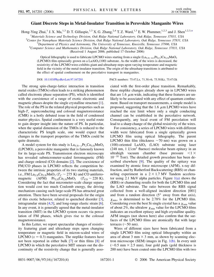
For consistency, a series of LPCMO wires with differentwidth were fabricated from a single epitaxially grownLPCMO film using optical lithography. The parentLPCMO thin film (thickness $70 nm) was grown on a(100)-oriented LaAlO3 (LAO) substrate using laser(248 nm, 1 J=cm2 fluence) molecular beam epitaxy in anultrahigh vacuum chamber (base pressure <1&10"10 Torr). The detailed growth procedure has been de-scribed elsewhere [9]. The quality of the epitaxy wasexamined by atomic force microscope (AFM), x-ray dif-fraction, and by Rutherford Backscattering (RBS) or chan-neling experiment in a 2& 1:7 MV Tandem accelera-tor using 2.1 MeV alpha particles. Figure 1(a) shows the(RBS) or channeling results for both the LPCMO film andthe LAO substrate. The ratio between the RBS signalcollected from a well-aligned incident direction [001]and from a random direction (5' away from that axis),"min, is determined to be 2.78% for the LPCMO film.Considering even the best Si single crystal has a "min valueof about 2%, the ultralow "min value for the LPCMO filmsindicates an excellent epitaxy and high crystalline quality.AFM images (not shown here) also confirm that the sur-faces of the LPCMO films are atomically flat with largeterraces ($50 nm).
Wires of different sizes have been fabricated from asingle LPCMO film using optical lithography within anarea of about 3 mm& 3 mm, as shown by scanning elec-tron microscope (SEM) images in Fig. 1(b). In every unit($0:5 mm& 2:5 mm), four gold pads (gold thickness is200 nm) have been coated onto the LPCMO film with two
PRL 97, 167201 (2006) P H Y S I C A L R E V I E W L E T T E R S week ending20 OCTOBER 2006
0031-9007=06=97(16)=167201(4) 167201-1 ! 2006 The American Physical Society
500 !m& 400 !m pads serving as current contacts andtwo 500 !m& 200 !m pads as voltage contacts. Theelectrical connections between the Au pads and the puckof a physical property measurement system were made byKulicke and Soffa wire bonders (model 4123 for Al and4124 for Au). Twenty microns diameter Au or Al wireswere directly engaged without using any paint and solder,which removes all possible contact problems for the trans-port measurements. Magnetic field was applied along theeasy magnetization axis, i.e., the direction perpendicular tothe substrate surface during the transport measurements.
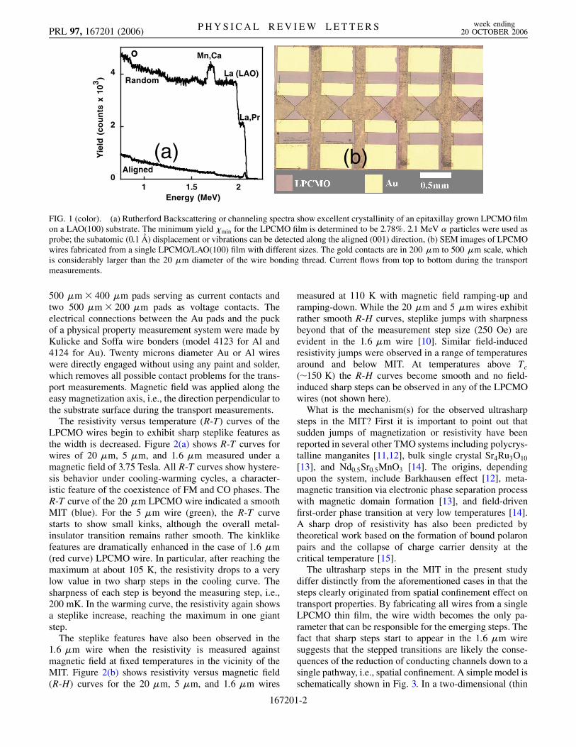
The resistivity versus temperature (R-T) curves of theLPCMO wires begin to exhibit sharp steplike features asthe width is decreased. Figure 2(a) shows R-T curves forwires of 20 !m, 5 !m, and 1:6 !m measured under amagnetic field of 3.75 Tesla. All R-T curves show hystere-sis behavior under cooling-warming cycles, a character-istic feature of the coexistence of FM and CO phases. TheR-T curve of the 20 !m LPCMO wire indicated a smoothMIT (blue). For the 5 !m wire (green), the R-T curvestarts to show small kinks, although the overall metal-insulator transition remains rather smooth. The kinklikefeatures are dramatically enhanced in the case of 1:6 !m(red curve) LPCMO wire. In particular, after reaching themaximum at about 105 K, the resistivity drops to a verylow value in two sharp steps in the cooling curve. Thesharpness of each step is beyond the measuring step, i.e.,200 mK. In the warming curve, the resistivity again showsa steplike increase, reaching the maximum in one giantstep.
The steplike features have also been observed in the1:6 !m wire when the resistivity is measured againstmagnetic field at fixed temperatures in the vicinity of theMIT. Figure 2(b) shows resistivity versus magnetic field(R-H) curves for the 20 !m, 5 !m, and 1:6 !m wires
measured at 110 K with magnetic field ramping-up andramping-down. While the 20 !m and 5 !m wires exhibitrather smooth R-H curves, steplike jumps with sharpnessbeyond that of the measurement step size (250 Oe) areevident in the 1:6 !m wire [10]. Similar field-inducedresistivity jumps were observed in a range of temperaturesaround and below MIT. At temperatures above Tc($150 K) the R-H curves become smooth and no field-induced sharp steps can be observed in any of the LPCMOwires (not shown here).
What is the mechanism(s) for the observed ultrasharpsteps in the MIT? First it is important to point out thatsudden jumps of magnetization or resistivity have beenreported in several other TMO systems including polycrys-talline manganites [11,12], bulk single crystal Sr4Ru3O10
[13], and Nd0:5Sr0:5MnO3 [14]. The origins, dependingupon the system, include Barkhausen effect [12], meta-magnetic transition via electronic phase separation processwith magnetic domain formation [13], and field-drivenfirst-order phase transition at very low temperatures [14].A sharp drop of resistivity has also been predicted bytheoretical work based on the formation of bound polaronpairs and the collapse of charge carrier density at thecritical temperature [15].
The ultrasharp steps in the MIT in the present studydiffer distinctly from the aforementioned cases in that thesteps clearly originated from spatial confinement effect ontransport properties. By fabricating all wires from a singleLPCMO thin film, the wire width becomes the only pa-rameter that can be responsible for the emerging steps. Thefact that sharp steps start to appear in the 1:6 !m wiresuggests that the stepped transitions are likely the conse-quences of the reduction of conducting channels down to asingle pathway, i.e., spatial confinement. A simple model isschematically shown in Fig. 3. In a two-dimensional (thin
0
2
4
1 1.5 2Energy (MeV)
Yie
ld(c
ount
sx
103 )
Mn,Ca
La (LAO)
La,Pr
OO
Random
Aligned
(a) (b)
FIG. 1 (color). (a) Rutherford Backscattering or channeling spectra show excellent crystallinity of an epitaxillay grown LPCMO filmon a LAO(100) substrate. The minimum yield "min for the LPCMO film is determined to be 2.78%. 2.1 MeV # particles were used asprobe; the subatomic (0.1 A) displacement or vibrations can be detected along the aligned (001) direction, (b) SEM images of LPCMOwires fabricated from a single LPCMO/LAO(100) film with different sizes. The gold contacts are in 200 !m to 500 !m scale, whichis considerably larger than the 20 !m diameter of the wire bonding thread. Current flows from top to bottom during the transportmeasurements.
PRL 97, 167201 (2006) P H Y S I C A L R E V I E W L E T T E R S week ending20 OCTOBER 2006
167201-2
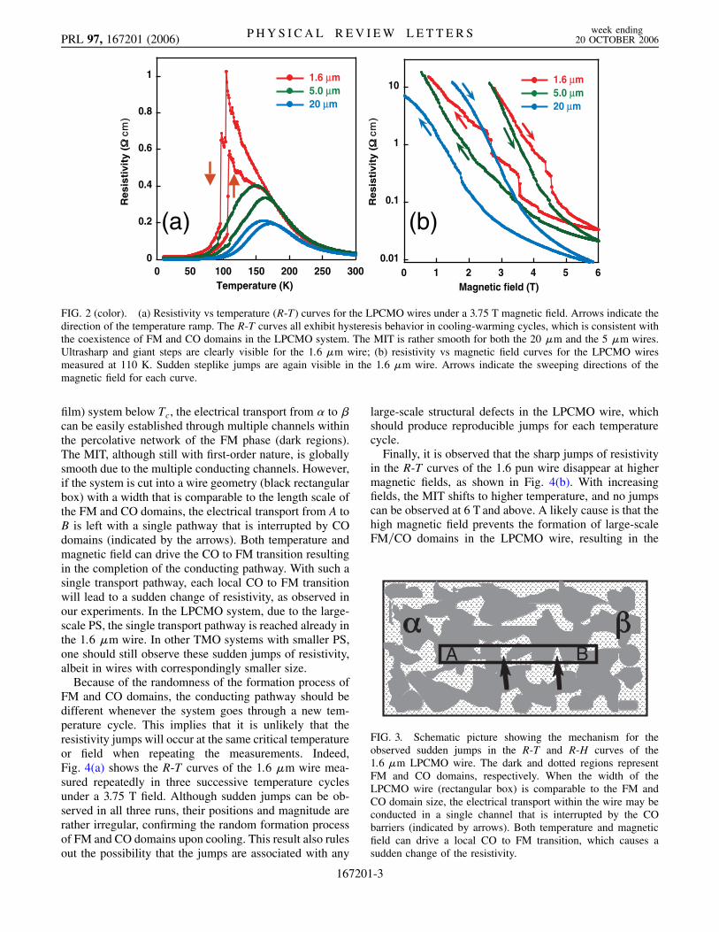
film) system below Tc, the electrical transport from # to $can be easily established through multiple channels withinthe percolative network of the FM phase (dark regions).The MIT, although still with first-order nature, is globallysmooth due to the multiple conducting channels. However,if the system is cut into a wire geometry (black rectangularbox) with a width that is comparable to the length scale ofthe FM and CO domains, the electrical transport from A toB is left with a single pathway that is interrupted by COdomains (indicated by the arrows). Both temperature andmagnetic field can drive the CO to FM transition resultingin the completion of the conducting pathway. With such asingle transport pathway, each local CO to FM transitionwill lead to a sudden change of resistivity, as observed inour experiments. In the LPCMO system, due to the large-scale PS, the single transport pathway is reached already inthe 1:6 !m wire. In other TMO systems with smaller PS,one should still observe these sudden jumps of resistivity,albeit in wires with correspondingly smaller size.
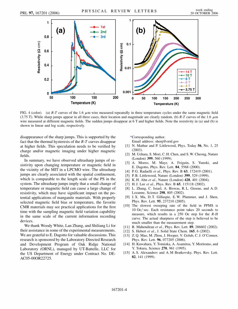
Because of the randomness of the formation process ofFM and CO domains, the conducting pathway should bedifferent whenever the system goes through a new tem-perature cycle. This implies that it is unlikely that theresistivity jumps will occur at the same critical temperatureor field when repeating the measurements. Indeed,Fig. 4(a) shows the R-T curves of the 1:6 !m wire mea-sured repeatedly in three successive temperature cyclesunder a 3.75 T field. Although sudden jumps can be ob-served in all three runs, their positions and magnitude arerather irregular, confirming the random formation processof FM and CO domains upon cooling. This result also rulesout the possibility that the jumps are associated with any
large-scale structural defects in the LPCMO wire, whichshould produce reproducible jumps for each temperaturecycle.
Finally, it is observed that the sharp jumps of resistivityin the R-T curves of the 1.6 pun wire disappear at highermagnetic fields, as shown in Fig. 4(b). With increasingfields, the MIT shifts to higher temperature, and no jumpscan be observed at 6 T and above. A likely cause is that thehigh magnetic field prevents the formation of large-scaleFM=CO domains in the LPCMO wire, resulting in the
A B
FIG. 3. Schematic picture showing the mechanism for theobserved sudden jumps in the R-T and R-H curves of the1:6 !m LPCMO wire. The dark and dotted regions representFM and CO domains, respectively. When the width of theLPCMO wire (rectangular box) is comparable to the FM andCO domain size, the electrical transport within the wire may beconducted in a single channel that is interrupted by the CObarriers (indicated by arrows). Both temperature and magneticfield can drive a local CO to FM transition, which causes asudden change of the resistivity.
0.01
0.1
1
10
0 1 2 3 4 5 6
Res
isti
vity
(cm
)
Magnetic field (T)
1.6 µm5.0 µm20 µm
0
0.2
0.4
0.6
0.8
1
0 50 100 150 200 250 300
Res
isti
vity
(cm
)
Temperature (K)
1.6 µm5.0 µm20 µm
(a) (b)
FIG. 2 (color). (a) Resistivity vs temperature (R-T) curves for the LPCMO wires under a 3.75 T magnetic field. Arrows indicate thedirection of the temperature ramp. The R-T curves all exhibit hysteresis behavior in cooling-warming cycles, which is consistent withthe coexistence of FM and CO domains in the LPCMO system. The MIT is rather smooth for both the 20 !m and the 5 !m wires.Ultrasharp and giant steps are clearly visible for the 1:6 !m wire; (b) resistivity vs magnetic field curves for the LPCMO wiresmeasured at 110 K. Sudden steplike jumps are again visible in the 1:6 !m wire. Arrows indicate the sweeping directions of themagnetic field for each curve.
PRL 97, 167201 (2006) P H Y S I C A L R E V I E W L E T T E R S week ending20 OCTOBER 2006
167201-3
disappearance of the sharp jumps. This is supported by thefact that the thermal hysteresis of the R-T curves disappearat higher fields. This speculation needs to be verified bycharge and/or magnetic imaging under higher magneticfields.
In summary, we have observed ultrasharp jumps of re-sistivity upon changing temperature or magnetic field inthe vicinity of the MIT in a LPCMO wire. The ultrasharpjumps are clearly associated with the spatial confinement,which is comparable to the length scale of the PS in thesystem. The ultrasharp jumps imply that a small change oftemperature or magnetic field can cause a large change ofresistivity, which may have significant impact on the po-tential applications of manganite materials. With properlyselected magnetic field bias or temperature, the favoriteCMR materials may see practical applications for the firsttime with the sampling magnetic field variation capabilityin the same scale of the current information recordingdevices.
We thank Woody White, Lan Zhang, and Shiliang Li fortheir assistance in some of the experimental measurements.We are grateful to E. Dagotto for valuable discussions. Thisresearch is sponsored by the Laboratory Directed Researchand Development Program of Oak Ridge NationalLaboratory (ORNL), managed by UT-Battelle, LLC forthe US Department of Energy under Contract No. DE-AC05-00OR22725.
*Corresponding author.Email address: [email protected]
[1] N. Mathur and P. Littlewood, Phys. Today 56, No. 1, 25(2003).
[2] M. Uehara, S. Mori, C. H. Chen, and S. W. Cheong, Nature(London) 399, 560 (1999).
[3] A. Moreo, M. Mayr, A. Feiguin, S. Yunoki, andE. Dagotto, Phys. Rev. Lett. 84, 5568 (2000).
[4] P. G. Radaelli et al., Phys. Rev. B 63, 172419 (2001).[5] P. B. Littlewood, Nature (London) 399, 529 (1999).[6] K. H. Ahn et al., Nature (London) 428, 401 (2004).[7] H. J. Lee et al., Phys. Rev. B 65, 115118 (2002).[8] L. Zhang, C. Israel, A. Biswas, R. L. Greene, and A. D.
Lozanne, Science 298, 805 (2002).[9] J. X. Ma, D. T. Gillaspie, E. W. Plummer, and J. Shen,
Phys. Rev. Lett. 95, 237210 (2005).[10] The slowest sweeping rate of the field in PPMS is
10 Oe= sec. Each resistance point takes 20 seconds tomeasure, which results in a 250 Oe step for the R-Hcurve. The actual sharpness of the step is believed to bemuch smaller than the measurement step.
[11] R. Mahendiran et al., Phys. Rev. Lett. 89, 286602 (2002).[12] S. Hebert et al., J. Solid State Chem. 165, 6 (2002).[13] Z. Q. Mao, M. Zhou, J. Hooper, V. Golub, C. J. O’Connor,
Phys. Rev. Lett. 96, 077205 (2006).[14] H. Kuwahara, Y. Tomioka, A. Asamitsu, Y. Moritomo, and
Y. Tokura, Science 270, 961 (1995).[15] A. S. Alexandrov and A. M Bratkovsky, Phys. Rev. Lett.
82, 141 (1999).
0
0.2
0.4
0.6
0.8
1
50 100 150 200Temperature (K)
1st2nd3rd
Re
sis
tiv
ity
(cm
)
0.001
0.01
0.1
1
0 50 100 150 200 250 300
14 T10 T8 T6 T4 T3.75 T
Res
isti
vity
(cm
)
Temperature (K)
(a) (b)
FIG. 4 (color). (a) R-T curves of the 1:6 !m wire measured repeatedly in three temperature cycles under the same magnetic field(3.75 T). While sharp jumps appear in all three cases, their location and magnitude are clearly random. (b) R-T curves of the 1:6 !mwire measured at different magnetic fields. The sudden jumps disappear at 6 T and higher fields. Note the resistivity in (a) and (b) isshown in linear and log scale, respectively.
PRL 97, 167201 (2006) P H Y S I C A L R E V I E W L E T T E R S week ending20 OCTOBER 2006
167201-4