Embed Size (px)
Citation preview

[email protected] Page 1 of 19
GIGALIGHT 100GBASE QSFP28 CWDM4 10KM
Optical Transceiver Module
P/N: GQS-SPO101-CLR4CA
Features
4 channels full-duplex transceiver modules
Transmission data rate up to 26Gbps per channel
4 x 26Gb/s DFB-based CWDM uncooled transmitter
4 channels PIN ROSA
Internal CDR circuits on both receiver and transmitter
channels
Non airtight optical engine design
Qualified under temperature 85°C and humidity 85%
@500 hours (the variation of TX≤2.5 dBm, RX≤1.5 dBm)
Low power consumption <3.5W
Hot Pluggable QSFP form factor
Up to reach 10km for G.652 SMF[with KR4 FEC]
Duplex LC receptacles
Built-in digital diagnostic functions
Operating case temperature 0°C to +70°C
3.3V power supply voltage
RoHS 6 compliant(lead free)
Applications
Data Center Interconnect.
100G 4WDM-10 10km reach.
100G CWDM4 applications.
Infiniband EDR interconnects.
Enterprise networking

[email protected] Page 2 of 19
Description
This product is a 100Gb/s transceiver module designed for optical communication applications
compliant with the QSFP MSA,CWDM4 MSA,100G 4WDM4-10 MSA and portions of IEEE
P802.3bm standard. The module converts 4 input channels of 25Gb/s electrical data to 4 channels
of CWDM optical signals and then multiplexes them into a single channel for 100Gb/s optical
transmission. Reversely on the receiver side, the module de-multiplexes a 100Gb/s optical input into 4
channels of CWDM optical signals and then converts them to 4 output channels of electrical data.
The central wavelengths of the 4 CWDM channels are 1271, 1291, 1311 and 1331 nm as members of
the CWDM wavelength grid defined in CWDM4 MSA and 4WDM4-10 MSA. The high performance
Uncooled CWDM DFB transmitters and high sensitivity PIN receivers provide superior performance for
100Gigabit Ethernet applications up to 10km links .
The product is designed with form factor, optical/electrical connection and digital diagnostic interface
according to the QSFP+ Multi-Source Agreement (MSA). It has been designed to meet the harshest
external operating conditions including temperature, humidity and EMI interference.
Figure1. Module Block Diagram

[email protected] Page 3 of 19
Absolute Maximum Ratings
Parameter Symbol Min Max Unit
Supply Voltage Vcc -0.3 3.6 V
Input Voltage Vin -0.3 Vcc+0.3 V
Storage Temperature Tst -20 85 ºC
Case Operating Temperature Top 0 70 ºC
Humidity(non-condensing) Rh 5 85 %
Damage Threshold, each Lane TH 5.5 dBm
Recommended Operating Conditions
Parameter Symbol Min Typical Max Unit
Supply Voltage Vcc 3.13 3.3 3.47 V
Operating Case temperature Tca 0 70 ºC
Data Rate Per Lane fd 25.78125 Gbps
Humidity Rh 5 85 %
Power Dissipation P 3.5 W
Link Distance with G.652 D 0.002 10 km
Electrical Specifications
Parameter Symbol Min Typical Max Unit
Power Consumption P 3.5 W
Supply Current Icc 1.12 A
Transceiver Power-on
Initialization Time
2000 ms
Transmitter(each Lane)
Single-ended Input Voltage
Tolerance -0.3 4.0 V
AC Common Mode Input Voltage
Tolerance 15 mV
Differential Input Voltage 50 mVpp
Differential Input Voltage Swing Vin 190 1000 mVpp
Differential Input Impedance Zin 90 100 110 Ohm
Receiver(each Lane)
Single-ended Output Voltage -0.3 4.0 V
AC Common Mode Output
Voltage 7.5 mV
Differential Output Voltage Swing Vout 300 900 mVpp
Differential Output Impedance Zout 90 100 110 Ohm
Note:Power-on Initialization Time is the time from when the power supply voltages reach and remain
above the minimum recommended operating supply voltages to the time when the module is fully

[email protected] Page 4 of 19
functional.
Optical Characteristics
Parameter Symbo
l Min Typical Max Unit Notes
Lane Wavelength
L0 1264.5 1271 1277.5 nm
L1 1284.5 1291 1297.5 nm
L2 1304.5 1311 1317.5 nm
L3 1324.5 1331 1337.5 nm
Transmitter
SMSR SMSR 30 dB
Total Average Launch Power PT 8.5 dBm
Average Launch Power,
each Lane PAVG -6.5 2.5 dBm
OMA, each Lane POMA -4.0 2.5 dBm 1
Launch power in OMA minus
TDP -5 dB
TDP, each Lane TDP 3.0 dB
Extinction Ratio ER 3.5 dB
RIN20OMA RIN -130 dB/H
z
Optical Return Loss
Tolerance
TOL 20 dB
Transmitter Reflectance RT -20 dB
Eye Mask coordinates:
X1, X2, X3, Y1, Y2, Y3 {0.31, 0.4, 0.45, 0.34, 0.38, 0.4} 2
Average Launch Power OFF
Transmitter, each Lane
Poff -30 dBm
Receiver
Damage Threshold, each lane THd 3.5 dBm 3
Average Receive Power, each
lane -13.0 2.5 dBm
Receive Power (OMA),
each lane 2.5 dBm
Receiver Sensitivity (OMA),
each Lane SEN -11.5 dBm 4

[email protected] Page 5 of 19
Stressed Receiver Sensitivity
(OMA), each Lane -8.6 dBm 5
LOS Assert LOSA -16 dBm
LOS Deassert LOSD -14 dBm
LOS Hysteresis LOSH 0.5 2 dB
Receiver Electrical 3 dB
upper Cutoff Frequency, each
Lane
Fc 31 GHz
Conditions of Stress Receiver Sensitivity Test (Note 5)
Vertical Eye Closure Penalty VECP 1.9 dB 6
Stressed Eye J2 Jitter J2 0.33 UI
Stressed Eye J4 Jitter, J4 0.48 UI
Note:
1. Even if the TDP < 1 dB, the OMA min must exceed the minimum value specified here.
2. Hit ratio of 5e-5, per IEEE; See Figure 2 below.
3. The receiver shall be able to tolerate, without damage, continuous exposure to a modulated
optical input signal having this power level on one lane. The receiver does not have to operate
correctly at this input power.
4. Measured with conformance test signal at receiver input for BER = 5e-5 BER.
5. Measured with 4WDM-10 MSA conformance test signal at TP3 for 5e-5BER.
6. Vertical eye closure penalty and stressed eye jitter are test conditions for measuring stressed
receiver sensitivity. They are not characteristics of the receiver.

[email protected] Page 6 of 19
Figure 2.Eye Mask
Pin Descriptions
Pin Logic Symbol Name/Description Ref.
1 GND Module Ground 1
2 CML-I Tx2- Transmitter inverted data input
3 CML-I Tx2+ Transmitter non-inverted data input
4 GND Module Ground 1
5 CML-I Tx4- Transmitter inverted data input
6 CML-I Tx4+ Transmitter non-inverted data input
7 GND Module Ground 1
8 LVTTL-I MODSEI
L Module Select 2
9 LVTTL-I ResetL Module Reset 2
10 VCCRx +3.3v Receiver Power Supply
11 LVCMOS-
I SCL 2-wire Serial interface clock 2
12 LVCMOS-
I/O SDA 2-wire Serial interface data 2
13 GND Module Ground 1
14 CML-O RX3+ Receiver non-inverted data output
15 CML-O RX3- Receiver inverted data output
16 GND Module Ground 1
17 CML-O RX1+ Receiver non-inverted data output
18 CML-O RX1- Receiver inverted data output
19 GND Module Ground 1

[email protected] Page 7 of 19
20 GND Module Ground 1
21 CML-O RX2- Receiver inverted data output
22 CML-O RX2+ Receiver non-inverted data output
23 GND Module Ground 1
24 CML-O RX4- Receiver inverted data output
25 CML-O RX4+ Receiver non-inverted data output
26 GND Module Ground 1
27 LVTTL-O ModPrsL Module Present, internal pulled down to GND
28 LVTTL-O IntL Interrupt output, should be pulled up on host board 2
29 VCCTx +3.3v Transmitter Power Supply
30 VCC1 +3.3v Power Supply
31 LVTTL-I LPMode Low Power Mode 2
32 GND Module Ground 1
33 CML-I Tx3+ Transmitter non-inverted data input
34 CML-I Tx3- Transmitter inverted data input
35 GND Module Ground 1
36 CML-I Tx1+ Transmitter non-inverted data input
37 CML-I Tx1- Transmitter inverted data input
38 GND Module Ground 1
Notes:
1. Module circuit ground is isolated from module chassis ground within the module.
2. Open collector; should be pulled up with 4.7k – 10k ohms on host board to a voltage between
3.15Vand 3.6V.
Figure3. Electrical Pin-out Details
ModSelL Pin
The ModSelL is an input pin. When held low by the host, the module responds to 2-wire serial
communication commands. The ModSelL allows the use of multiple QSFP modules on a single 2-wire

[email protected] Page 8 of 19
interface bus. When the ModSelL is “High”, the module will not respond to any 2-wire interface
communication from the host.ModSelL has an internal pull-up in the module.
ResetL Pin
Reset. LPMode_Reset has an internal pull-up in the module. A low level on the ResetL pin for longer
than the minimum pulse length (t_Reset_init) initiates a complete module reset, returning all user
module settings to their default state. Module Reset Assert Time (t_init) starts on the rising edge after the
low level on the
ResetL pin is released. During the execution of a reset (t_init) the host shall disregard all status bits until
the module indicates a completion of the reset interrupt. The module indicates this by posting an IntL
signal with the Data_Not_Ready bit negated. Note that on power up (including hot insertion) the module
will post this completion of reset interrupt without requiring a reset.
LPMode Pin
Gigalight QSFP28 CWDM4 operate in the low power mode (less than 1.5 W power consumption).This
pin active high will decrease power consumption to less than 1W.
ModPrsL Pin
ModPrsL is pulled up to Vcc on the host board and grounded in the module. The ModPrsL is asserted
“Low” when the module is inserted and deasserted “High” when the module is physically absent from
the host connector.
IntL Pin
IntL is an output pin. When “Low”, it indicates a possible module operational fault or a status critical to
the host system. The host identifies the source of the interrupt by using the 2-wire serial interface. The
IntL pin is an open collector output and must be pulled up to Vcc on the host board.
Power Supply Filtering
The host board should use the power supply filtering shown in Figure 4.
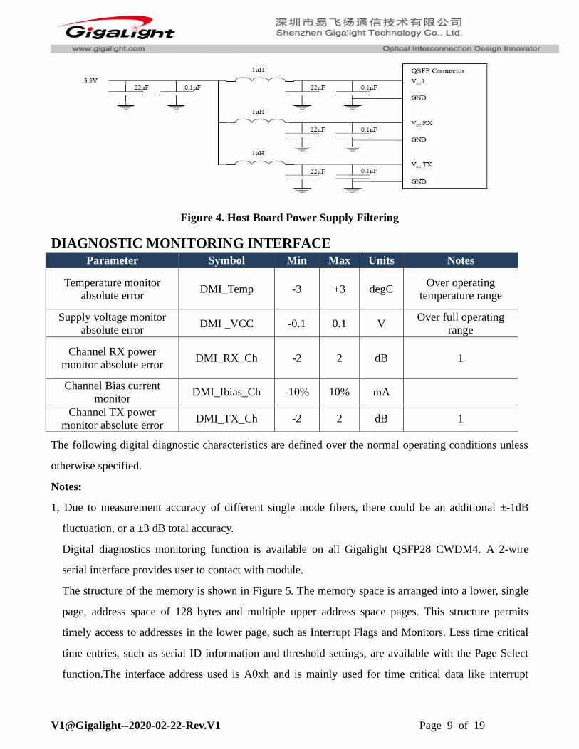
[email protected] Page 9 of 19
Figure 4. Host Board Power Supply Filtering
DIAGNOSTIC MONITORING INTERFACE
The following digital diagnostic characteristics are defined over the normal operating conditions unless
otherwise specified.
Notes:
1, Due to measurement accuracy of different single mode fibers, there could be an additional ±-1dB
fluctuation, or a ±3 dB total accuracy.
Digital diagnostics monitoring function is available on all Gigalight QSFP28 CWDM4. A 2-wire
serial interface provides user to contact with module.
The structure of the memory is shown in Figure 5. The memory space is arranged into a lower, single
page, address space of 128 bytes and multiple upper address space pages. This structure permits
timely access to addresses in the lower page, such as Interrupt Flags and Monitors. Less time critical
time entries, such as serial ID information and threshold settings, are available with the Page Select
function.The interface address used is A0xh and is mainly used for time critical data like interrupt
Parameter Symbol Min Max Units Notes
Temperature monitor
absolute error DMI_Temp -3 +3 degC
Over operating
temperature range
Supply voltage monitor
absolute error DMI _VCC -0.1 0.1 V
Over full operating
range
Channel RX power
monitor absolute error DMI_RX_Ch -2 2 dB 1
Channel Bias current
monitor DMI_Ibias_Ch -10% 10% mA
Channel TX power
monitor absolute error DMI_TX_Ch -2 2 dB 1

[email protected] Page 10 of 19
handling in order to enable a one-time-read for all data related to an interrupt situation. After an
interrupt, IntL, has been asserted, the host can read out the flag field to determine the affected channel
and type of flag.
Figure5. QSFP Memory Map

[email protected] Page 12 of 19
Figure 8. Page 00 Memory Map
Page02 is User EEPROM and its format decided by user. The detail description of low memory and
page00.page03 upper memory please see SFF-8436 and SFF-8636 document.
SFF-8636 Specification

[email protected] Page 13 of 19
TX AND RX CDR LOL indicator (Byte 5)
TX AND RX CDR BYPASS CONTROL (Byte 98)

[email protected] Page 14 of 19

[email protected] Page 15 of 19
Timing for Soft Control and Status Functions Parameter Symbol Max Unit Conditions
Initialization Time t_init 2000 ms Time from power on1, hot plug or rising edge
of Reset until the module is fully functional2
Reset Init Assert
Time t_reset_init 2 μs
A Reset is generated by a low level longer
than the minimum reset pulse time present on
the ResetL pin.
Serial Bus Hardware
Ready Time t_serial 2000 ms
Time from power on1 until module responds
to data transmission over the 2-wire serial
bus
Monitor Data Ready
Time t_data 2000 ms
Time from power on1 to data not ready, bit 0
of Byte 2, deasserted and IntL asserted
Reset Assert Time t_reset 2000 ms Time from rising edge on the ResetL pin
until the module is fully functional2
LPMode Assert Time ton_LPMode 100 μs
Time from assertion of LPMode
(Vin:LPMode = Vih) until module power
consumption enters lower Power Level
IntL Assert Time ton_IntL 200 ms Time from occurrence of condition triggering
IntL until Vout:IntL = Vol
IntL Deassert Time toff_IntL 500 μs
Time from clear on read3 operation of
associated flag until Vout:IntL = Voh. This
includes deassert times for Rx LOS, Tx Fault
and other flag bits.
Rx LOS Assert Time ton_los 100 ms Time from Rx LOS state to Rx LOS bit set
and IntL asserted
Tx Fault Assert Time ton_Txfault 200 ms Time from Tx Fault state to Tx Fault bit set
and IntL asserted
Flag Assert Time ton_flag 200 ms
Time from occurrence of condition triggering
flag to associated flag bit set and IntL
asserted

[email protected] Page 16 of 19
Mask Assert Time ton_mask 100 ms Time from mask bit set4 until associated IntL
assertion is inhibited
Mask Deassert Time toff_mask 100 ms Time from mask bit cleared4 until associated
IntlL operation resumes
ModSelL Assert
Time ton_ModSelL 100 μs
Time from assertion of ModSelL until
module responds to data transmission over
the 2-wire serial bus
ModSelL Deassert
Time
toff_ModSelL
100 μs
Time from deassertion of ModSelL until the
module does not respond to data
transmission over the 2-wire serial bus
Power_over-ride or
Power-set Assert
Time
ton_Pdown 100 ms
Time from P_Down bit set 4 until module
power consumption enters lower Power
Level
Power_over-ride or
Power-set Deassert
Time
toff_Pdown 300 ms Time from P_Down bit cleared4 until the
module is fully functional3
Note:
1. Power on is defined as the instant when supply voltages reach and remain at or above the minimum
specified value.
2. Fully functional is defined as IntL asserted due to data not ready bit, bit 0 byte 2 deasserted.
3. Measured from falling clock edge after stop bit of read transaction.
4. Measured from falling clock edge after stop bit of write transaction.

[email protected] Page 17 of 19
Mechanical Dimensions
Figure 9 . Mechanical Specifications
Ordering information Part Number Product Description
GQS-SPO101- CLR4CA 100GE, QSFP28, 100GBASE CWDM4 2km
References
1. SFF-8436.
2. SFF-8636.
3. SFF-8431.
4. SFF-8665.
5. 100G CWDM4 MSA.
6. 100G 4WDM-10 MSA
7. IEEE 802.3bm.
8. IEEE 802.3ba.

[email protected] Page 18 of 19
ESD
This transceiver is specified as ESD threshold 1kV for SFI pins and 2kV for all other electrical input
pins, tested per MIL-STD-883, Method 3015.4 /JESD22-A114-A (HBM). However, normal ESD
precautions are still required during the handling of this module. This transceiver is shipped in ESD
protective packaging. It should be removed from the packaging and handled only in an ESD protected
environment.
Laser Safety
This is a Class 1 Laser Product according to IEC 60825-1:2007. This product complies with 21 CFR
1040.10 and 1040.11 except for deviations pursuant to Laser Notice No. 50, dated (June 24, 2007).
Important Notice
Performance figures, data and any illustrative material provided in this data sheet are typical and must be
specifically confirmed in writing by GIGALIGHT before they become applicable to any particular order
orcontract. In accordance with the GIGALIGHT policy of continuous improvement specifications may
change without notice.
The publication of information in this data sheet does not imply freedom from patent or other protective
rights of GIGALIGHT or others. Further details are available from any GIGALIGHT sales
representative.
Email:[email protected]
http://www.gigalight.com
Revision History
Revision Level Date Description
V0 Preliminary OCT-16- 2018 Advance Release.
V1 Revised 2020/02/22 PN: GQS-SPO101-CIR4C to be GQS-SPO101-CLR4CA
CAUTION:
Use of controls or adjustment or performance of procedures other than those specified herein may
result in hazardous radiation exposure

[email protected] Page 19 of 19