Embed Size (px)
Citation preview
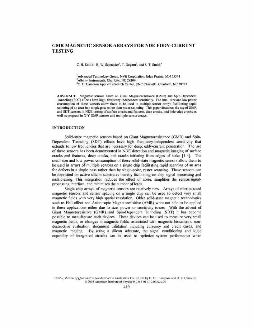
GMR MAGNETIC SENSOR ARRAYS FOR NDE EDDY-CURRENTTESTING
C. H. Smith1, R. W. Schneider1, T. Dogaru2, and S. T. Smith3
Advanced Technology Group, NVE Corporation, Eden Prairie, MN 553442Albany Instruments, Charlotte, NC 282093C. C. Cameron Applied Research Center, UNC Charlotte, Charlotte, NC 28223
ABSTRACT. Magnetic sensors based on Giant Magnetoresistance (GMR) and Spin-DependentTunneling (SDT) effects have high, frequency-independent sensitivity. The small size and low powerconsumption of these sensors allow them to be used in multiple-sensor arrays facilitating rapidscanning of an area in a single pass rather than raster scanning. This paper discusses the use of GMRand SDT sensors in NDE testing of surface cracks and features, deep cracks, and hole-edge cracks aswell as progress in X-Y GMR sensors and multiple-sensor arrays.
INTRODUCTION
Solid-state magnetic sensors based on Giant Magnetoresistance (GMR) and Spin-Dependent Tunneling (SDT) effects have high, frequency-independent sensitivity thatextends to low frequencies that are necessary for deep, eddy-current penetration. The useof these sensors has been demonstrated in NDE detection and magnetic imaging of surfacecracks and features, deep cracks, and cracks initiating from edges of holes [1-4]. Thesmall size and low power consumption of these solid-state magnetic sensors allow them tobe used in arrays of multiple sensors on a single chip facilitating rapid scanning of an areafor defects in a single pass rather than by single-point, raster scanning. These sensors canbe deposited on active silicon substrates thereby facilitating on-chip signal processing andmultiplexing. This integration reduces the effect of noise, simplifies the sensor/signal-processing interface, and minimizes the number of leads.
Single-chip arrays of magnetic sensors are relatively new. Arrays of micron-sizedmagnetic sensors and sensor spacing on a single chip can be used to detect very smallmagnetic fields with very high spatial resolution. Older solid-state magnetic technologiessuch as Hall-effect and Anisotropic Magnetoresisitive (AMR) were not able to be appliedin these applications either due to size, power or sensitivity issues. With the advent ofGiant Magnetoresistive (GMR) and Spin-Dependent Tunneling (SDT) it has becomepossible to manufacture such devices. These devices can be used to measure very smallmagnetic fields, or changes in magnetic fields, associated with magnetic biosensors, non-destructive evaluation, document validation including currency and credit cards, andmagnetic imaging. By using a silicon substrate, the signal conditioning and logiccapability of integrated circuits can be used to optimize system performance when
CP657, Review of Quantitative Nondestructive Evaluation Vol. 22, ed. by D. O. Thompson and D. E. Chimenti© 2003 American Institute of Physics 0-7354-0117-9/03/S20.00
419
compared to a collection of sensors supplying raw signals to a processor. This integratedtechnique reduces the effect of noise and simplifies the sensor/signal-processing interface.
SENSOR ELEMENTS
High-resolution arrays with a large number of elements require extremely smallsensing elements that operate at low power levels. GMR materials can be lithographicallypatterned in the form of simple resistors, half bridges, or full Wheatstone bridges.
Single resistor elements are the smallest devices and require the fewestconnections. They can be separate or can be connected in series with a differentialamplifier across each resistor. They have poor temperature compensation and usuallyrequire the formation of some type of bridge by using external components.
Half bridges take up twice the space but offer some temperature compensation dueto the fact that both resistors are at the same temperature. Half bridges can be used as fieldgradient sensors if one of the resistors is physically separated from the other by somedistance. They can function as field sensors if one of the resistors is shielded from theapplied field. The number of external connections to an array of N half-bridge elementscan be as low as N+2 including supply and ground.
Full bridges require four resistors per sensor. Small magnetic shields plated overtwo of the four equal resistors in a Wheatstone bridge protect these resistors from theapplied field and allow them to act as reference resistors. Since all resistors are fabricatedfrom the same material, they have the same temperature coefficient as the active resistors.The two remaining resistors are both exposed to the external field. The bridge output ofsuch a bridge is twice the output from a bridge with only one active resistor. The outputfor a 16% change in these resistors is approximately 8% of the voltage applied to thebridge. Arrays of full bridges require more chip area than simple resistors or half bridges.In addition they require more interconnects and connections to the outside world. An arrayof A''full bridges requires 2N+2 connections.
If there is sufficient room on the chip magnetoresistive materials can be made moresensitive by adding permalloy structures plated onto the substrate act as flux concentrators.The active resistors are placed in the gap between two flux concentrators. These resistorsexperience a field that is larger than the applied field by approximately the ratio of the gapD between the flux concentrators to the length / of one of the flux concentrators, D/l. Insome cases the flux concentrators are also used as the aforementioned shields by placingthe two reference resistors beneath them.
GMR AND SDT MATERIALS
Giant Magnetoresistive (GMR) and Spin Dependent Tunneling (SDT) materialsexhibit large changes in resistance in the presence of a magnetic field. Their thin-filmnature allows the fabrication of extremely small sensors using traditional photolithographytechniques from the semiconductor industry. The fundamentals of GMR and SDTmaterials have been covered in previous papers [5,6]. Only the basics will be cover thebasics here. The large changes in resistance with magnetic field are associated with achange in magnetic scattering of the conduction electrons at interfaces between the layersin these structures. If adjacent magnetic layers are magnetized in the same direction thereis little magnetic scattering; if adjacent magnetic layers are magnetized in oppositedirections, there is maximum magnetic scattering.
420
Anti-parallel alignment can be achieved in alternating layers of magnetic andconductive materials if the conducting layers are the proper thickness. At a fewnanometers thickness, the magnetic layers couple anti-ferromagnetically. These multilayerGMR materials achieve maximum resistance in zero field and decreased resistance inapplied fields. To achieve a change in resistance of 10 to 20 %, several repetitions of themagnetic and non-magnetic layers are used providing multiple interfaces for magneticscattering to occur. Although the current flows predominantly in the plane of the thin film,the conduction electrons encounter the interfaces a sufficient number of times for themagnetic scattering to be noticeable. Typical commercial multilayer materials exhibitmaximum decreases in resistance of 10 to 20 % with applied fields of 50 to 300 Oe (4 to2.4 kA/m.
Spin dependent tunneling (SDT) structures are a recent addition to materialsexhibiting a large change in resistance. In contrast to GMR structures, SDT structuresutilize a thin insulating layer to separate two magnetic layers. Conduction is allowed byquantum tunneling through the insulator. The size of the tunneling current between the twomagnetic layers is modulated by the angle between the magnetization vectors in the twolayers. An antiferromagnet layer pins the adjacent magnetic layers. An A12O3 layer isused for the insulator, and the bottom magnetic layer is free to follow the applied magneticfield. The addition of an orthogonal bias field perpendicular to the pinned magnetic layerreduces hysteresis and results in a bipolar sensor. In the absence of an applied field, thedirection of magnetization of the free layer is perpendicular to that of the pinned layer.Fields along the sense axis, which is parallel to the pinned layer, decrease that anglemaking the layers more parallel and decrease the resistance. Fields in the oppositedirection increase the angle and increase the resistance.
Changes of resistance with magnetic field of 10 to >40 % have been observed inSDT structures. The field required for maximum change in resistance depends upon thecomposition of the magnetic layers and the method of achieving antiparallel alignment.Values of saturation field range from 0.1 to 10 kA/m (1.25 to 125 Oe) offering at the lowend, the possibility of extremely sensitive magnetic sensors.
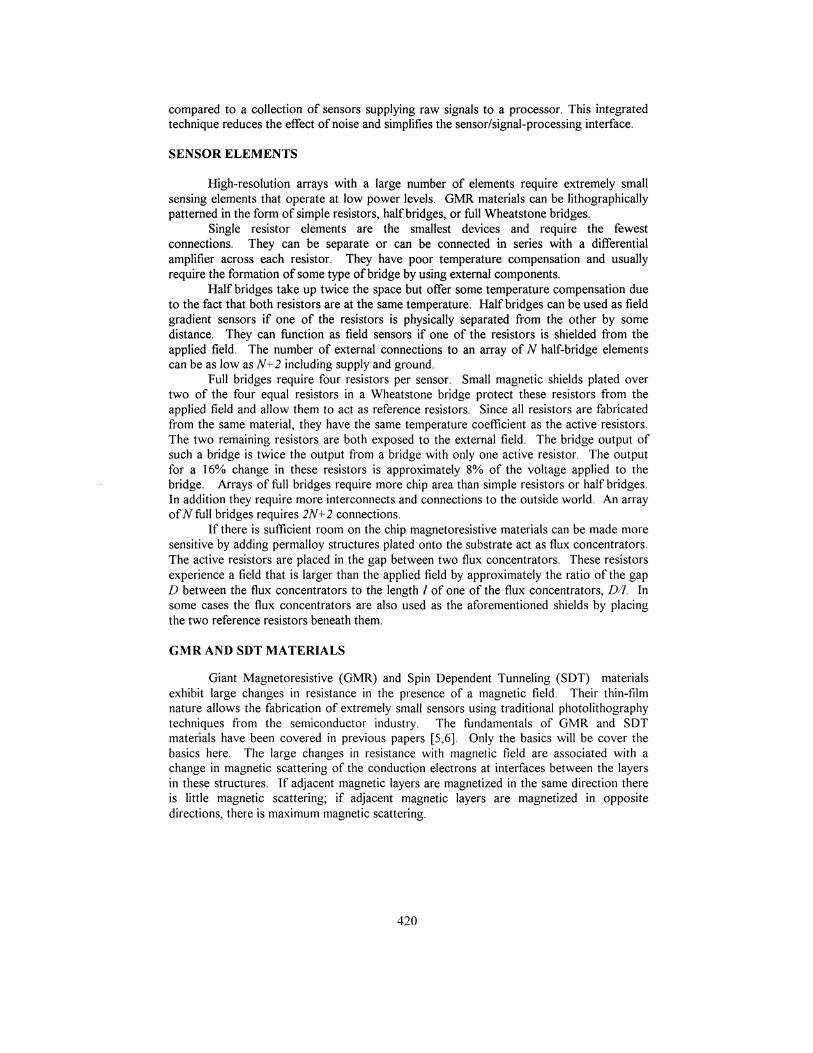
A comparison of magnetoresistive sensors is shown in Figure 1. Traces are shownfor an AMR sensor, GMR sensors both with and without flux concentrators, and aprototype SDT sensor. The portion below 4 Oe is enlarged on the right. Note that theGMR sensors are omnipolar and can not tell the difference between positive and negativefields unless they are magnetically biased away from their zero.
Out
put (
mV
/V)
XX^
-40
_
20tr—— B— •
— 4 —100\ 1 ./'
~,X-5
-'!
j£^^0
D / 1
——— 0 ——
X4-1'
20
4. AMR
.^.GMR/FluxConc0 Biased SDT
~
40
——
1-200
Field (Oe)
FIGURE 1. Comparison of AMR, GMR, and SDT sensors. The portion of the traces below 4 Oe isenlarged at the right.
421
SENSOR ARRAYS
Arrays can be used to build up an image of the magnetic fields in 1 and 2 and even3 orthogonal directions over an extended area. A 2-D image can be generated by passing alinear array of sensors over the surface. In contrast, the information from a 2-D array ofsensors tens of cm on a side can be used to image of a large area without moving the array.
GMR and SDT sensors are ideal for array applications because of their very smallsize and low power requirements. Typical GMR multilayer material has a sheet resistanceof about 10 ohms per square. This material can be patterned into stripes as narrow as 2 jamwide without causing significant magnetic edge effects. A 100-ohm resistor can befabricated which is only 20jim long. Larger resistors or resistors sensing a wider area canbe fabricated by forming serpentine stripes of longer length. These small dimensions areessential when multiple sensors are required for an array with high resolution.
Narrow stripes of multilayer material are sensitive to magnetic fields only alongtheir long dimension. Demagnetizing fields prevent fields along their width or thicknessfrom having a significant effect. The narrow stripes also allow arrays with much higherresolution than are possible with anisotropic magnetoresistive (AMR) materials. AMRmaterials are typically used in stripes 20 urn wide to sense fields transverse to the stripe
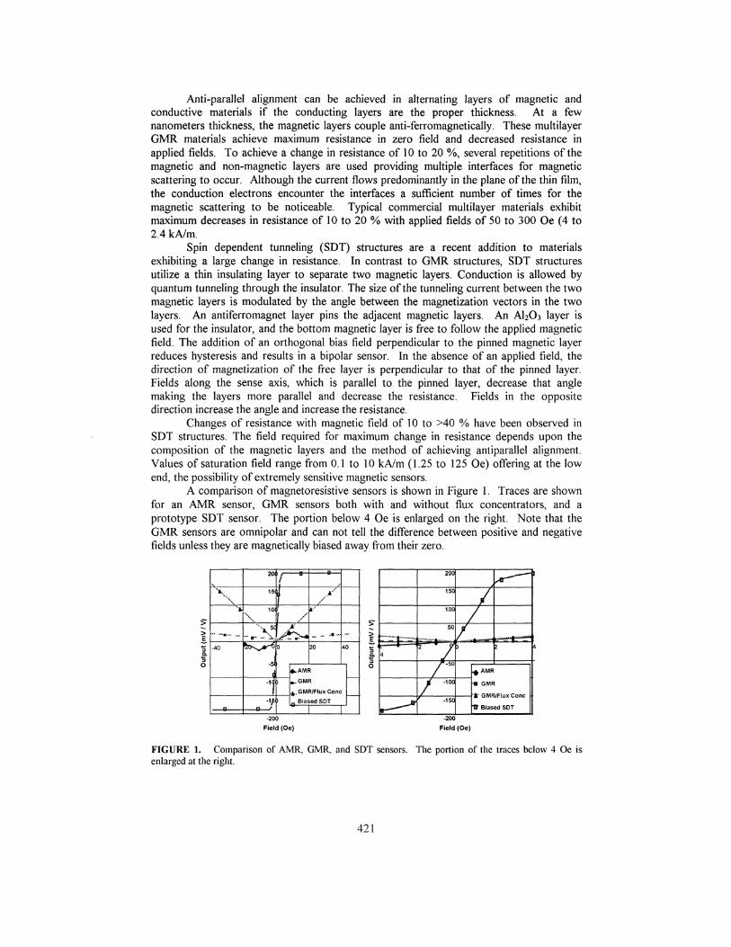
An example of a simple array of resistors is shown in the upper part of Figure 2.This 16-element array has one sensor each 5 jim for a total width of 80 jam. The structureson each side are lap-line monitors to allow the array to be lapped to the end of sensorelements. This array was designed to image information stored on magnetic media bydetecting the vertical component of the field with the sensor held immediately above amagnetic tape. The 1-mm by 2-mm size of this die is dictated by the number of bondingpads for the array and lap-line monitors.
FIGURE 2. A 16-element array of resistor elements with 5 jam spacing is shown in the upper portion. Totalactive width is 80 jam. Individual elements of the 5 ja,m array shown on the right. A 16-element array ofhalf-bridge resistor elements with 15 jam spacing is shown in the lower portion. Total active width is 240jam. Individual elements are shown on the right. The lower resistor elements are 4-stripe serpentineresistors with a repetition period of 15 jum.
422
The GMR stripes for the array with 5 um period in Figure 2 are 1.5 are |im wideand 6 jam long so they have a resistance of about 40 ohms each. They have a commonground. A current strap runs transversely above them in order to apply a bias field. Amore sophisticated 16-element linear array of half bridges is shown in the lower part ofFigure 1 with the detail of the individual half bridges shown on the right. This array has acommon supply as well as a common ground while the center of each half-bridge inconnected to a pad.
The GMR serpentine resistors 15 urn period in Figure 2 are also 1.5 urn wide andhave a total length of 18 um so they have a resistance of 120 ohms each. The upperresistor of the half bridges are hidden under the connection to the center of the half bridge.The upper resistors consist of a single stripe 18 um long. The 16-half bridges have acommon ground which is attached to a pad on the left and a common supply which isattached to a pad on the right. A current strap runs transversely above them in order toapply a bias field.
Linear arrays of GMR sensors can be used for detecting defects in ferromagneticmaterials by detecting flux leakage due to the defects [7]. A one-dimensional scan using a20-element GMR sensor resulted in a two-dimensional image.
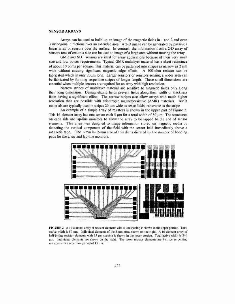
Another type of array is the X-Y sensor, which uses two sensors to measure boththe X-component of the field and the Y-component of the field at the same point. Onesuch sensor is shown in Figure 3. Both sensors are full Wheatstone bridges with twoactive resistors and two shielded, reference resistors.
The serpentine sensing resistors (shown as black boxes in the diagram) are locatedbetween flux concentrators, and the reference resistors are located under shields (shown asoblong open boxes). The sensitive direction of the resistors is transverse to their longdimension because the resistors are made up of multiple narrow stripes whose longdimension is transverse to the long dimension of the entire resistor. The interleaved sensorelements are connected as two independent Wheatstone bridges. This 2 mm by 2 mm diehas room for larger flux concentrators than the 3:1 shown.
FIGURE 3. Composite diagram including all mask layers for two-axis multilayer GMR sensor. Plated NiFeshields are shown over the serpentine reference resistors near the periphery of the chip. The sensing resistorsare shown in the center in the gaps between 3:1 flux concentrators
423
APPLICATIONS OF SDT/GMR ARRAYS IN NDE
The main components of an eddy current probe for NDE comprise a pancake-typecoil and a GMR or SDT sensor. During measurement the sensing axis of the GMR or SDTprobe is maintained to be coplanar with the surface of the specimen. The excitation fieldon the coil axis, being perpendicular to the sensing axis of the GMR or SDT films, has noeffect on the sensor. In this way, the detected field, which is the result of the perturbationof the eddy current flow paths due to the crack, is separated from the excitation field. Dueto the circular symmetry of the field produced by the coil, corresponding eddy currentsinduced in the surface of a defect free specimen are also circular. In this case, thetangential component of the field created by the eddy currents is zero at the location of thesensor. In the presence of defects, the probe provides an absolute measure of the perturbededdy currents.
The size of the coil is related to the resolution necessary to detect the defects. Forlarge defects and for deep defects, large coils surrounding the sensor are required. Toresolve small defects, small coils located close to the specimen are necessary. It ispossible to incorporate the excitation coils directly on GMR or SDT sensors.
Eddy currents shield the interior of the conducting material with the skin depthrelated to the conductivity and the frequency. Therefore, by changing the frequency,differing depths of the material can be probed. GMR or SDT sensors with their widefrequency response from dc into the multi-megahertz range are well suited to thisapplication. The small size of a GMR sensing element increases the resolution of defectlocation if the detector is raster scanned over the surface [3].
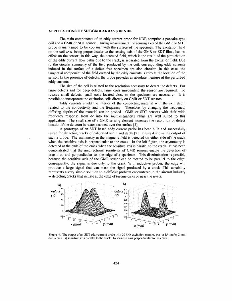
A prototype of an SDT based eddy current probe has been built and successfullytested for detecting cracks of calibrated width and depth [2]. Figure 4 shows the output ofsuch a probe. The asymmetry in the magnetic field is detected on either side of the crackwhen the sensitive axis is perpendicular to the crack. In the left figure, the asymmetry isdetected at the ends of the crack when the sensitive axis is parallel to the crack. It has beendemonstrated that the unidirectional sensitivity of GMR sensors enable the detection ofcracks at, and perpendicular to, the edge of a specimen. This discrimination is possiblebecause the sensitive axis of the GMR sensor can be rotated to be parallel to the edge;consequently, the signal is due only to the crack. With inductive probes, the edge willproduce a large signal that can mask the signal produced by a crack. This capabilityrepresents a very simple solution to a difficult problem encountered in the aircraft industry— detecting cracks that initiate at the edge of turbine disks or near the rivets.
x(mm) y (mm) x(mm) y (mm)
Figure 4. The output of an SDT eddy-current probe with 20 kHz excitation scanned over a 15 mm by 2 mmdeep crack, a) sensitive axis parallel to the crack, b) sensitive axis perpendicular to the crack.
424
150Output (mV) 100
500
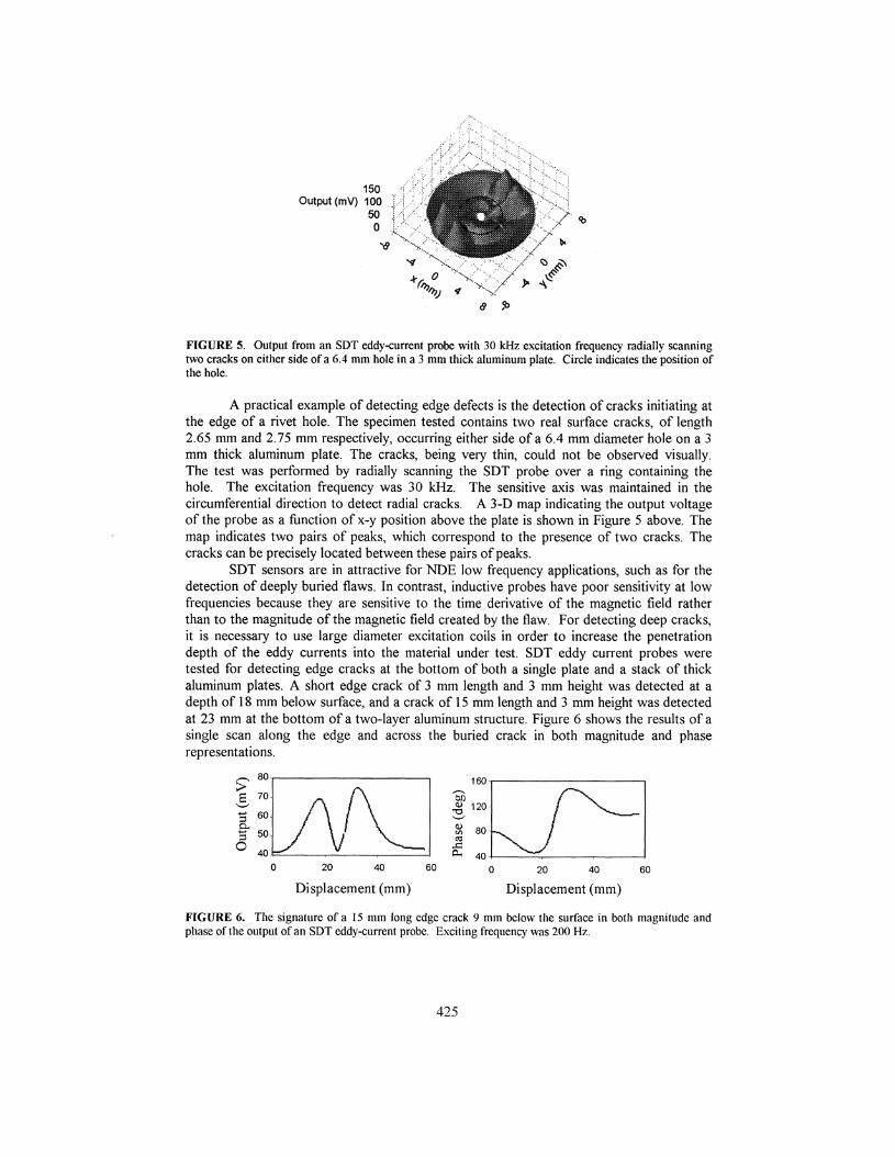
FIGURE 5. Output from an SDT eddy-current probe with 30 kHz excitation frequency radially scanningtwo cracks on either side of a 6.4 mm hole in a 3 mm thick aluminum plate. Circle indicates the position ofthe hole.
A practical example of detecting edge defects is the detection of cracks initiating atthe edge of a rivet hole. The specimen tested contains two real surface cracks, of length2.65 mm and 2.75 mm respectively, occurring either side of a 6.4 mm diameter hole on a 3mm thick aluminum plate. The cracks, being very thin, could not be observed visually.The test was performed by radially scanning the SDT probe over a ring containing thehole. The excitation frequency was 30 kHz. The sensitive axis was maintained in thecircumferential direction to detect radial cracks. A 3-D map indicating the output voltageof the probe as a function of x-y position above the plate is shown in Figure 5 above. Themap indicates two pairs of peaks, which correspond to the presence of two cracks. Thecracks can be precisely located between these pairs of peaks.
SDT sensors are in attractive for NDE low frequency applications, such as for thedetection of deeply buried flaws. In contrast, inductive probes have poor sensitivity at lowfrequencies because they are sensitive to the time derivative of the magnetic field ratherthan to the magnitude of the magnetic field created by the flaw. For detecting deep cracks,it is necessary to use large diameter excitation coils in order to increase the penetrationdepth of the eddy currents into the material under test. SDT eddy current probes weretested for detecting edge cracks at the bottom of both a single plate and a stack of thickaluminum plates. A short edge crack of 3 mm length and 3 mm height was detected at adepth of 18 mm below surface, and a crack of 15 mm length and 3 mm height was detectedat 23 mm at the bottom of a two-layer aluminum structure. Figure 6 shows the results of asingle scan along the edge and across the buried crack in both magnitude and phaserepresentations.
,-x 80
£ 7°g 60-d,g so0 40
160
12CH
on80
4020 40 60 20 40 60
Displacement (mm) Displacement (mm)
FIGURE 6. The signature of a 15 mm long edge crack 9 mm below the surface in both magnitude andphase of the output of an SDT eddy-current probe. Exciting frequency was 200 Hz.
425
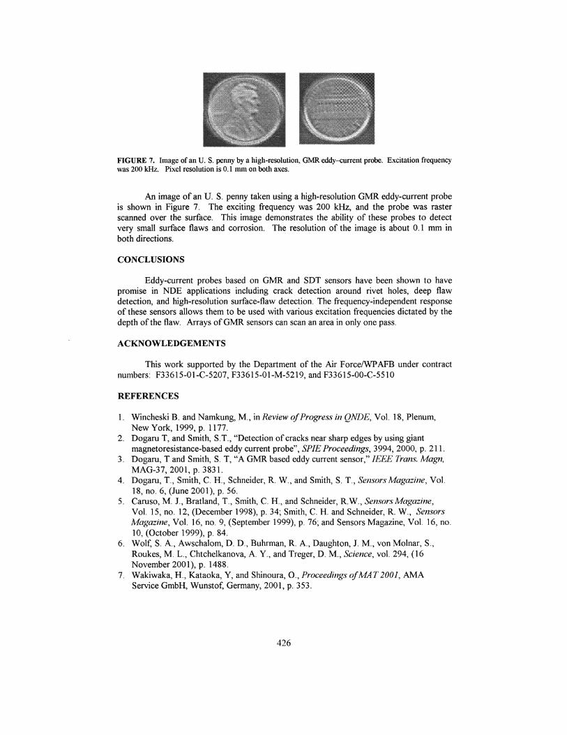
FIGURE 7. Image of an U. S. penny by a high-resolution, GMR eddy-current probe. Excitation frequencywas 200 kHz. Pixel resolution is 0.1 mm on both axes.
An image of an U. S. penny taken using a high-resolution GMR eddy-current probeis shown in Figure 7. The exciting frequency was 200 kHz, and the probe was rasterscanned over the surface. This image demonstrates the ability of these probes to detectvery small surface flaws and corrosion. The resolution of the image is about 0.1 mm inboth directions.
CONCLUSIONS
Eddy-current probes based on GMR and SDT sensors have been shown to havepromise in NDE applications including crack detection around rivet holes, deep flawdetection, and high-resolution surface-flaw detection. The frequency-independent responseof these sensors allows them to be used with various excitation frequencies dictated by thedepth of the flaw. Arrays of GMR sensors can scan an area in only one pass.
ACKNOWLEDGEMENTS
This work supported by the Department of the Air Force/WPAFB under contractnumbers: F33615-01-C-5207, F33615-01-M-5219, andF33615-00-C-5510
REFERENCES
1. Wincheski B. and Namkung, M., in Review of Progress in ONDE, Vol. 18, Plenum,New York, 1999, p. 1177.
2. Dogaru T, and Smith, S.T., "Detection of cracks near sharp edges by using giantmagnetoresistance-based eddy current probe", SPIE Proceedings, 3994, 2000, p. 211.
3. Dogaru, T and Smith, S. T, "A GMR based eddy current sensor," IEEE Tram. Magn,MAG-37, 2001, p. 3831.
4. Dogaru, T., Smith, C. H., Schneider, R. W., and Smith, S. T., Sensors Magazine, Vol.18, no. 6, (June 2001), p. 56.
5. Caruso, M. J., Bratland, T., Smith, C. H., and Schneider, R.W., Sensors Magazine,Vol. 15, no. 12, (December 1998), p. 34; Smith, C. H. and Schneider, R. W., SensorsMagazine, Vol. 16, no. 9, (September 1999), p. 76; and Sensors Magazine, Vol. 16, no.10, (October 1999), p. 84.
6. Wolf, S. A., Awschalom, D. D., Buhrman, R. A., Daughton, J. M., von Molnar, S.,Roukes, M. L., Chtchelkanova, A. Y., and Treger, D. M., Science, vol. 294, (16November 2001), p. 1488.
7. Wakiwaka, H., Kataoka, Y, and Shinoura, O., Proceedings of MAT 2001, AMAService GmbH, Wunstof, Germany, 2001, p. 353.
426