Embed Size (px)
Citation preview

© 2011 ANSYS, Inc. September 8, 20111
Thermal Management of Electronics in Drilling and Completion
Gokul V Shankaran
© 2011 ANSYS, Inc. September 8, 20112
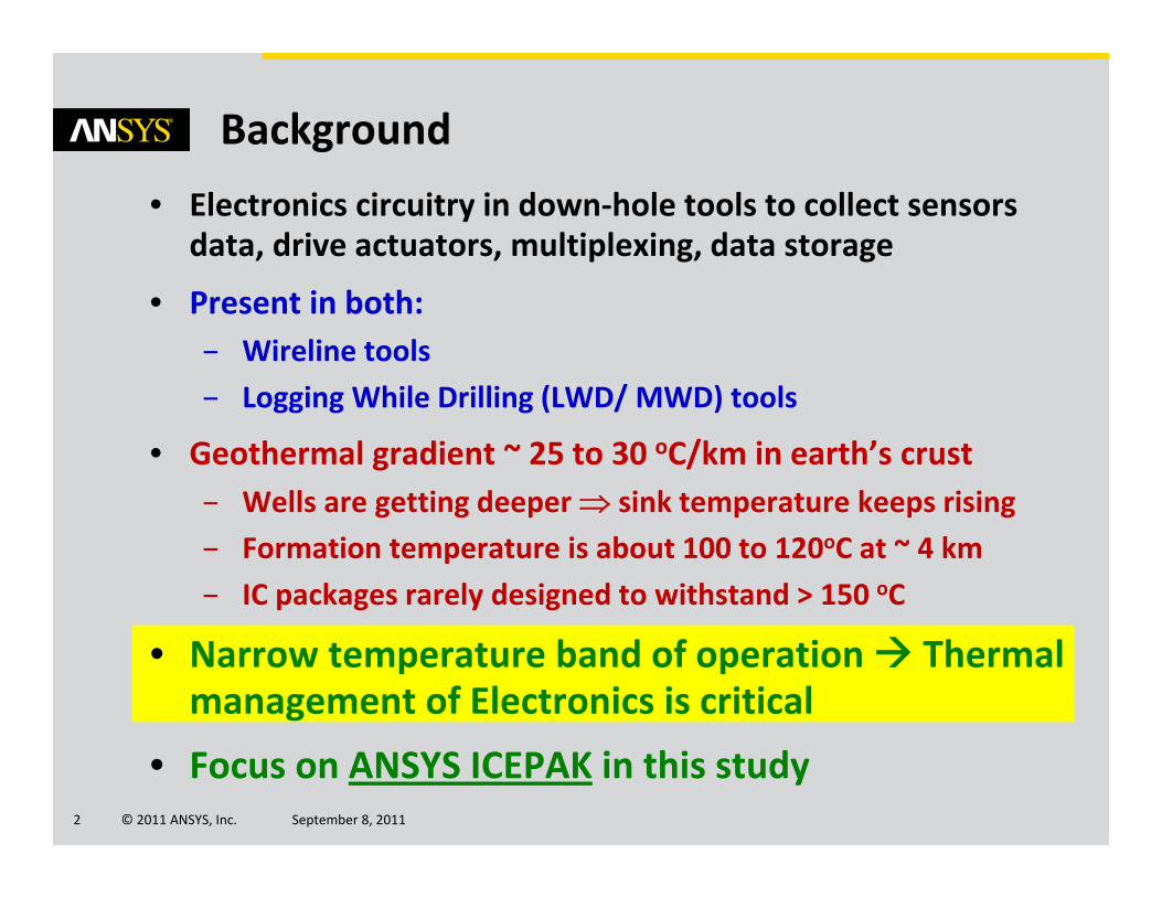
• Electronics circuitry in down‐hole tools to collect sensors data, drive actuators, multiplexing, data storage
• Present in both:– Wireline tools– Logging While Drilling (LWD/ MWD) tools
• Geothermal gradient ~ 25 to 30 oC/km in earth’s crust– Wells are getting deeper sink temperature keeps rising– Formation temperature is about 100 to 120oC at ~ 4 km– IC packages rarely designed to withstand > 150 oC
• Narrow temperature band of operation Thermal management of Electronics is critical
• Focus on ANSYS ICEPAK in this study
Background

© 2011 ANSYS, Inc. September 8, 20113
• WIRELINE TOOLSTRING – 7’ long, 2.5” dia
• Houses 16” Electronic Sectioncontaining:– PCB with ICs: Power = 11.1 W– IGBT FETs x 3: Power = 11 W ea– Actuator device: Power = 4 W
• Tool string studied in 8” dia well– Natural convection in well fluid– Natural convection and radiation within electronic section of tool
Case Study: Problem Description ‐ I
© 2011 ANSYS, Inc. September 8, 20114
IGBT heat sink
PCB (11.1 W)
IGBT (11 W) x 3
Actuator (4 W)
Core for mounting parts
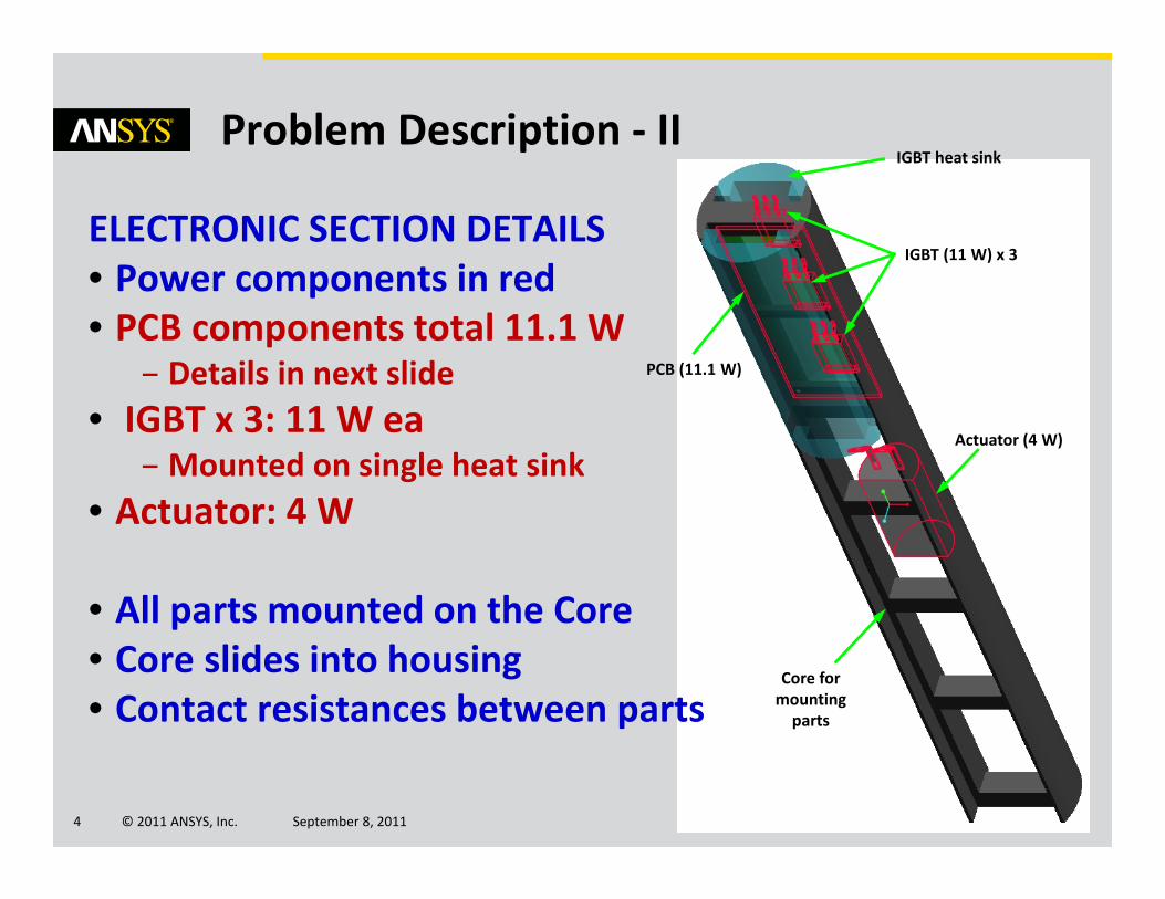
ELECTRONIC SECTION DETAILS• Power components in red• PCB components total 11.1 W
– Details in next slide• IGBT x 3: 11 W ea
– Mounted on single heat sink• Actuator: 4 W
• All parts mounted on the Core• Core slides into housing• Contact resistances between parts
Problem Description ‐ II
© 2011 ANSYS, Inc. September 8, 20115
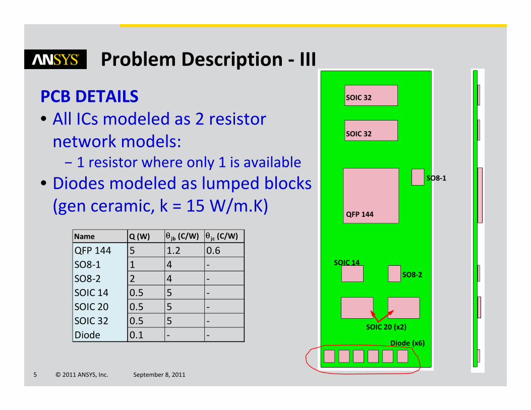
PCB DETAILS• All ICs modeled as 2 resistor network models:
– 1 resistor where only 1 is available• Diodes modeled as lumped blocks (gen ceramic, k = 15 W/m.K)
Problem Description ‐ III
SOIC 32
SOIC 14
Diode (x6)
SOIC 20 (x2)
QFP 144
SO8‐2
SO8‐1
SOIC 32
Name Q (W) jb (C/W) jc (C/W)
QFP 144 5 1.2 0.6SO8‐1 1 4 ‐SO8‐2 2 4 ‐SOIC 14 0.5 5 ‐SOIC 20 0.5 5 ‐SOIC 32 0.5 5 ‐Diode 0.1 ‐ ‐
© 2011 ANSYS, Inc. September 8, 20116
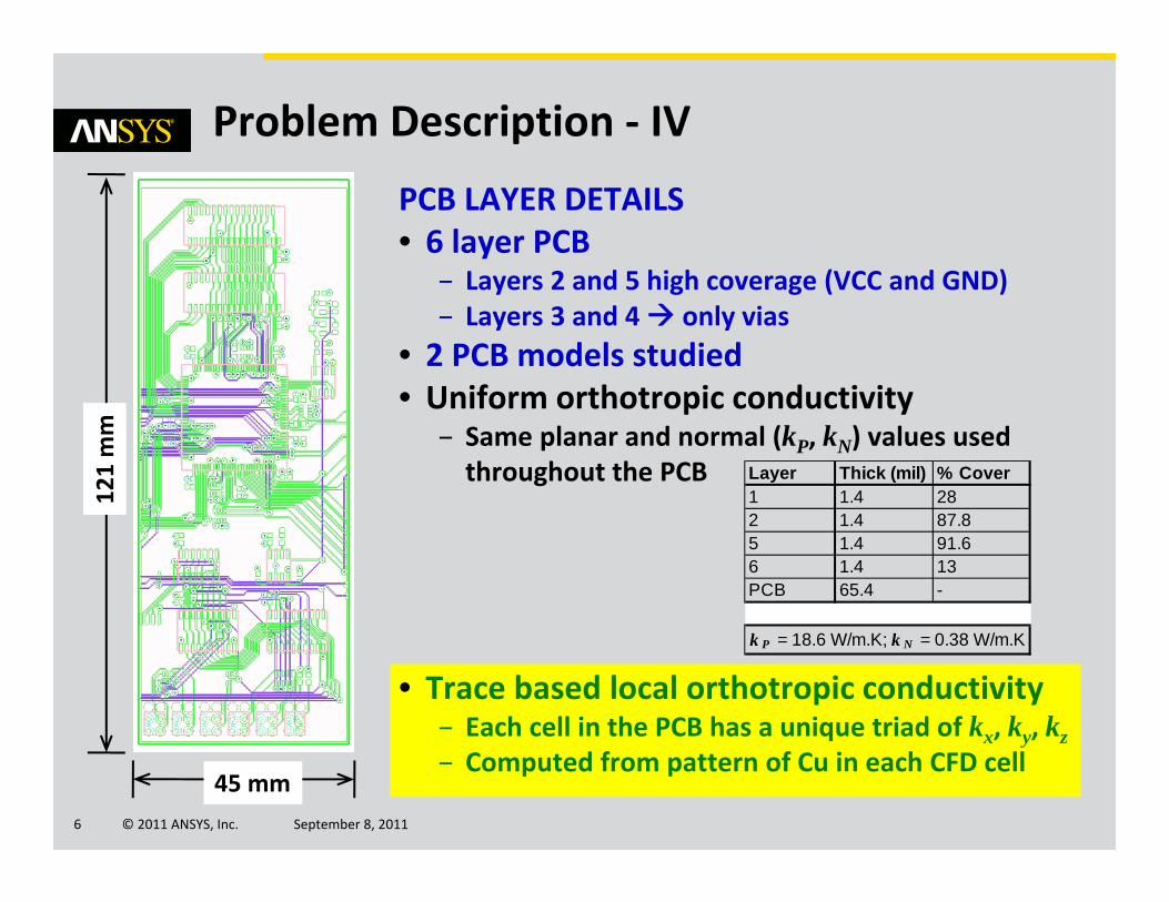
PCB LAYER DETAILS• 6 layer PCB
– Layers 2 and 5 high coverage (VCC and GND)– Layers 3 and 4 only vias
• 2 PCB models studied• Uniform orthotropic conductivity
– Same planar and normal (kP, kN) values used throughout the PCB
• Trace based local orthotropic conductivity– Each cell in the PCB has a unique triad of kx, ky, kz– Computed from pattern of Cu in each CFD cell
Problem Description ‐ IV
45 mm
121 mm
Layer Thick (mil) % Cover1 1.4 282 1.4 87.85 1.4 91.66 1.4 13PCB 65.4 -
k P = 18.6 W/m.K; k N = 0.38 W/m.K
© 2011 ANSYS, Inc. September 8, 20117
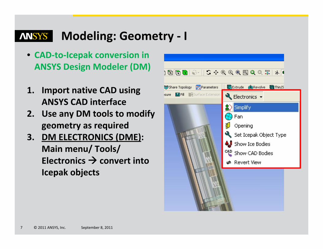
• CAD‐to‐Icepak conversion in ANSYS Design Modeler (DM)
1. Import native CAD using ANSYS CAD interface
2. Use any DM tools to modify geometry as required
3. DM ELECTRONICS (DME): Main menu/ Tools/ Electronics convert into Icepak objects
Modeling: Geometry ‐ I
© 2011 ANSYS, Inc. September 8, 20118
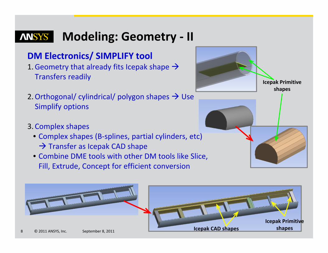
DM Electronics/ SIMPLIFY tool1.Geometry that already fits Icepak shape Transfers readily
2.Orthogonal/ cylindrical/ polygon shapes Use Simplify options
3. Complex shapes• Complex shapes (B‐splines, partial cylinders, etc) Transfer as Icepak CAD shape
• Combine DME tools with other DM tools like Slice, Fill, Extrude, Concept for efficient conversion
Modeling: Geometry ‐ II
Icepak Primitive shapes
Icepak CAD shapesIcepak Primitive
shapes
© 2011 ANSYS, Inc. September 8, 20119
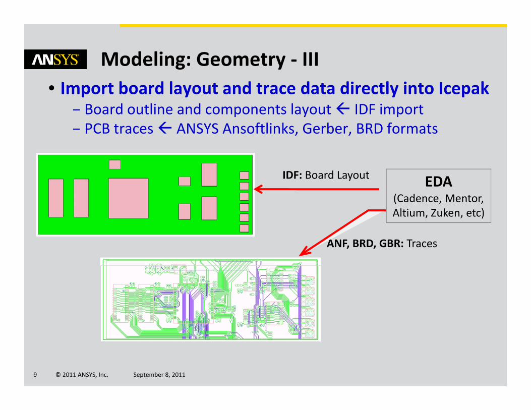
• Import board layout and trace data directly into Icepak– Board outline and components layout IDF import– PCB traces ANSYS Ansoftlinks, Gerber, BRD formats
Modeling: Geometry ‐ III
EDA(Cadence, Mentor, Altium, Zuken, etc)
IDF: Board Layout
ANF, BRD, GBR: Traces
© 2011 ANSYS, Inc. September 8, 201110
PCB
IGBT
Actuator
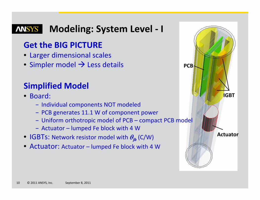
Get the BIG PICTURE• Larger dimensional scales• Simpler model Less details
Simplified Model• Board:
– Individual components NOT modeled– PCB generates 11.1 W of component power– Uniform orthotropic model of PCB – compact PCB model– Actuator – lumped Fe block with 4 W
• IGBTs: Network resistor model with jb (C/W)• Actuator: Actuator – lumped Fe block with 4 W
Modeling: System Level ‐ I

© 2011 ANSYS, Inc. September 8, 201111
• Model full tool string in well – Big picture– Capture overall heat flow from tool surface to well fluid– Well fluid circulation patterns ‐ well (domain) sizing– Consider all possible well conditions External to tool
Well fluid properties, non‐Newtonian, etcDifferent formation temperature conditionsTool orientation – gravity directionDo we have to model natural convection and radiation within the tool
Modeling: System Level ‐ II

© 2011 ANSYS, Inc. September 8, 201112
• 4 Different cases considered:i. Top and Bottom – Open; gravity: m/s2ii. Bottom at fixed 100oC, Top open; m/s2iii. Same as ii, but m/s2iv. Bottom at fixed 100oC, Top adiabatic wall
• Well fluid is the cylindrical CFD domain– Material: Liquid water– Height: 20’ in Cases i, ii, iii, 36’ in Case iv
• Boundary Conditions– Fixed Temp: 100 oC on Curved side of domain
• Cases i to iii identify worst scenario• Case iv proper well sizing
Modeling: System Level ‐ III
Well fluid
Electronic section of Tool
Domain top BC
Domain bottom BC
jg ˆ8.9
jg ˆ8.9
kg ˆ8.9
© 2011 ANSYS, Inc. September 8, 201113
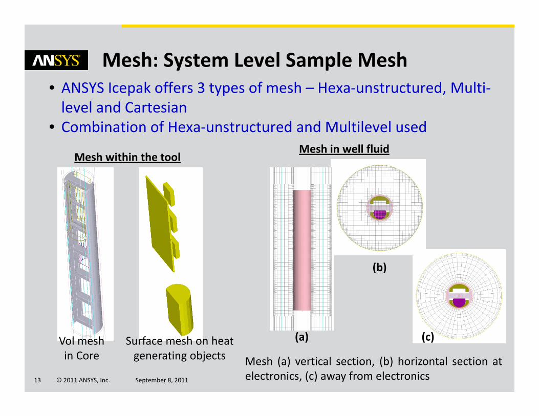
• ANSYS Icepak offers 3 types of mesh – Hexa‐unstructured, Multi‐level and Cartesian
• Combination of Hexa‐unstructured and Multilevel used
Mesh: System Level Sample Mesh
Mesh within the tool
Vol mesh in Core
Surface mesh on heat generating objects
Mesh in well fluid
Mesh (a) vertical section, (b) horizontal section atelectronics, (c) away from electronics
(a) (c)
(b)
© 2011 ANSYS, Inc. September 8, 201114
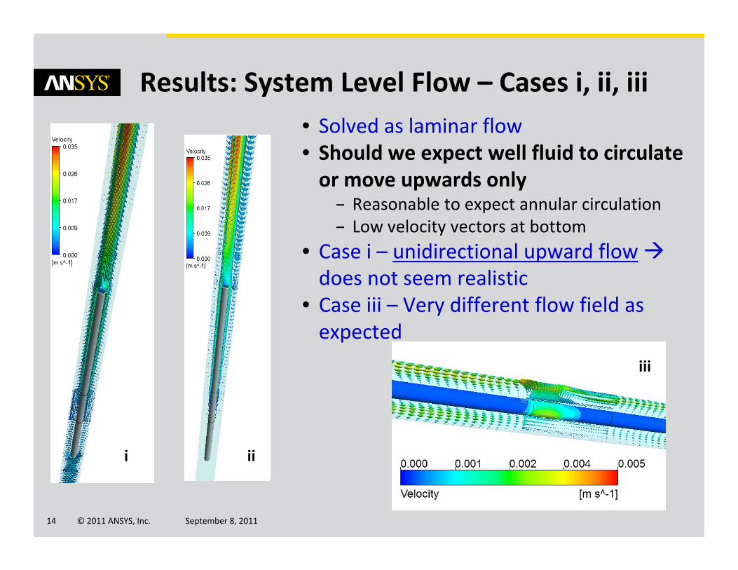
• Solved as laminar flow• Should we expect well fluid to circulate or move upwards only
– Reasonable to expect annular circulation– Low velocity vectors at bottom
• Case i – unidirectional upward flowdoes not seem realistic
• Case iii – Very different flow field as expected
Results: System Level Flow – Cases i, ii, iii
iii
iii

© 2011 ANSYS, Inc. September 8, 201115
• Temperatures compared for IGBTs and PCB• Temperatures in cases i, ii are similar• Case iii turns out to be cooler for the present tool
• Thus case ii may be considered as the worst case scenario• Problems with case ii:
– Top opening too close to tool – may numerically influence flow field– Complete recirculation is not visible
• Capturing complete recirculation field may require well model to extend more above the tool –work around in Case iv
Results: System Level Thermal – Cases i, ii, iii
Component Case i Case ii Case iiiigbt.1 110.4 110.5 108.7igbt.2 110.5 110.6 108.9igbt.3 110.2 110.2 108.8PCB 116.4 116.5 114.8
Component Temperatures in oC; igbt refers to junction
© 2011 ANSYS, Inc. September 8, 201116
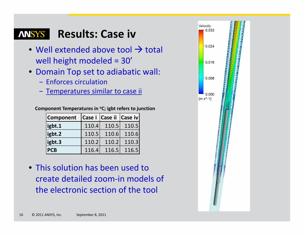
• Well extended above tool total well height modeled = 30’
• Domain Top set to adiabatic wall:– Enforces circulation– Temperatures similar to case ii
• This solution has been used to create detailed zoom‐in models of the electronic section of the tool
Results: Case iv
Component Case i Case ii Case ivigbt.1 110.4 110.5 110.5igbt.2 110.5 110.6 110.6igbt.3 110.2 110.2 110.3PCB 116.4 116.5 116.5
Component Temperatures in oC; igbt refers to junction
© 2011 ANSYS, Inc. September 8, 201117
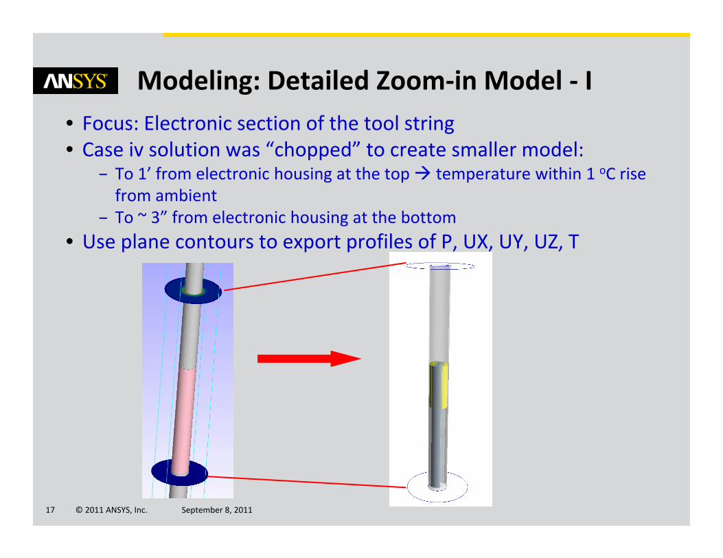
• Focus: Electronic section of the tool string• Case iv solution was “chopped” to create smaller model:
– To 1’ from electronic housing at the top temperature within 1 oC rise from ambient
– To ~ 3” from electronic housing at the bottom• Use plane contours to export profiles of P, UX, UY, UZ, T
Modeling: Detailed Zoom‐in Model ‐ I
© 2011 ANSYS, Inc. September 8, 201118
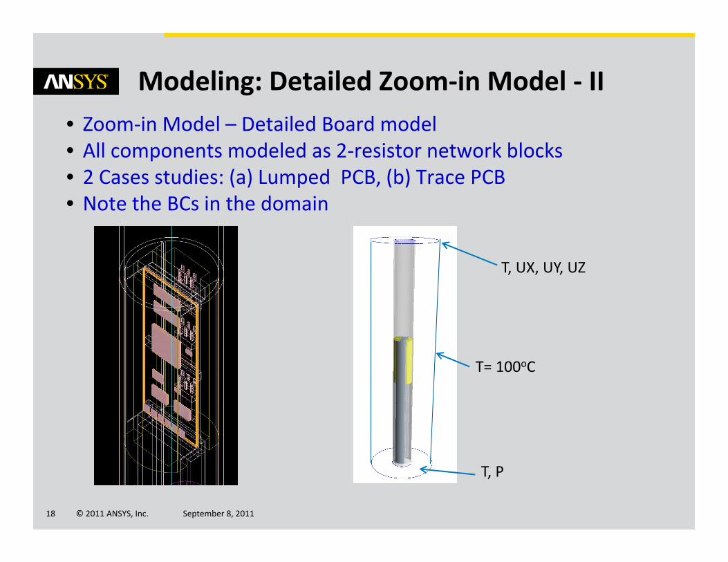
• Zoom‐in Model – Detailed Board model• All components modeled as 2‐resistor network blocks• 2 Cases studies: (a) Lumped PCB, (b) Trace PCB• Note the BCs in the domain
Modeling: Detailed Zoom‐in Model ‐ II
T, UX, UY, UZ
T= 100oC
T, P
© 2011 ANSYS, Inc. September 8, 201119
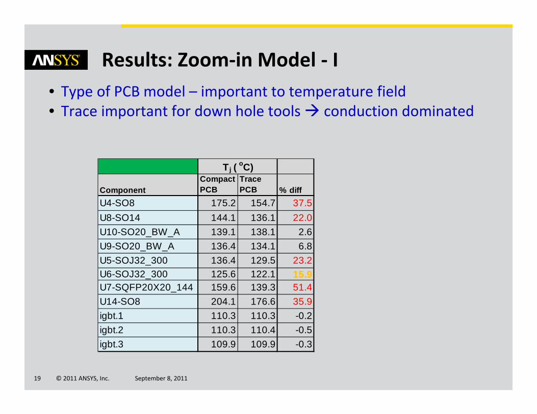
• Type of PCB model – important to temperature field• Trace important for down hole tools conduction dominated
Results: Zoom‐in Model ‐ I
ComponentCompact PCB
Trace PCB % diff
U4-SO8 175.2 154.7 37.5U8-SO14 144.1 136.1 22.0U10-SO20_BW_A 139.1 138.1 2.6U9-SO20_BW_A 136.4 134.1 6.8U5-SOJ32_300 136.4 129.5 23.2U6-SOJ32_300 125.6 122.1 15.9U7-SQFP20X20_144 159.6 139.3 51.4U14-SO8 204.1 176.6 35.9igbt.1 110.3 110.3 -0.2igbt.2 110.3 110.4 -0.5igbt.3 109.9 109.9 -0.3
Tj ( oC)
© 2011 ANSYS, Inc. September 8, 201120
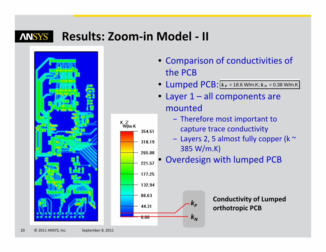
• Comparison of conductivities of the PCB
• Lumped PCB: • Layer 1 – all components are mounted
– Therefore most important to capture trace conductivity
– Layers 2, 5 almost fully copper (k ~ 385 W/m.K)
• Overdesign with lumped PCB
Results: Zoom‐in Model ‐ II
k P = 18.6 W/m.K; k N = 0.38 W/m.K
kP
kN
Conductivity of Lumped orthotropic PCB
© 2011 ANSYS, Inc. September 8, 201121
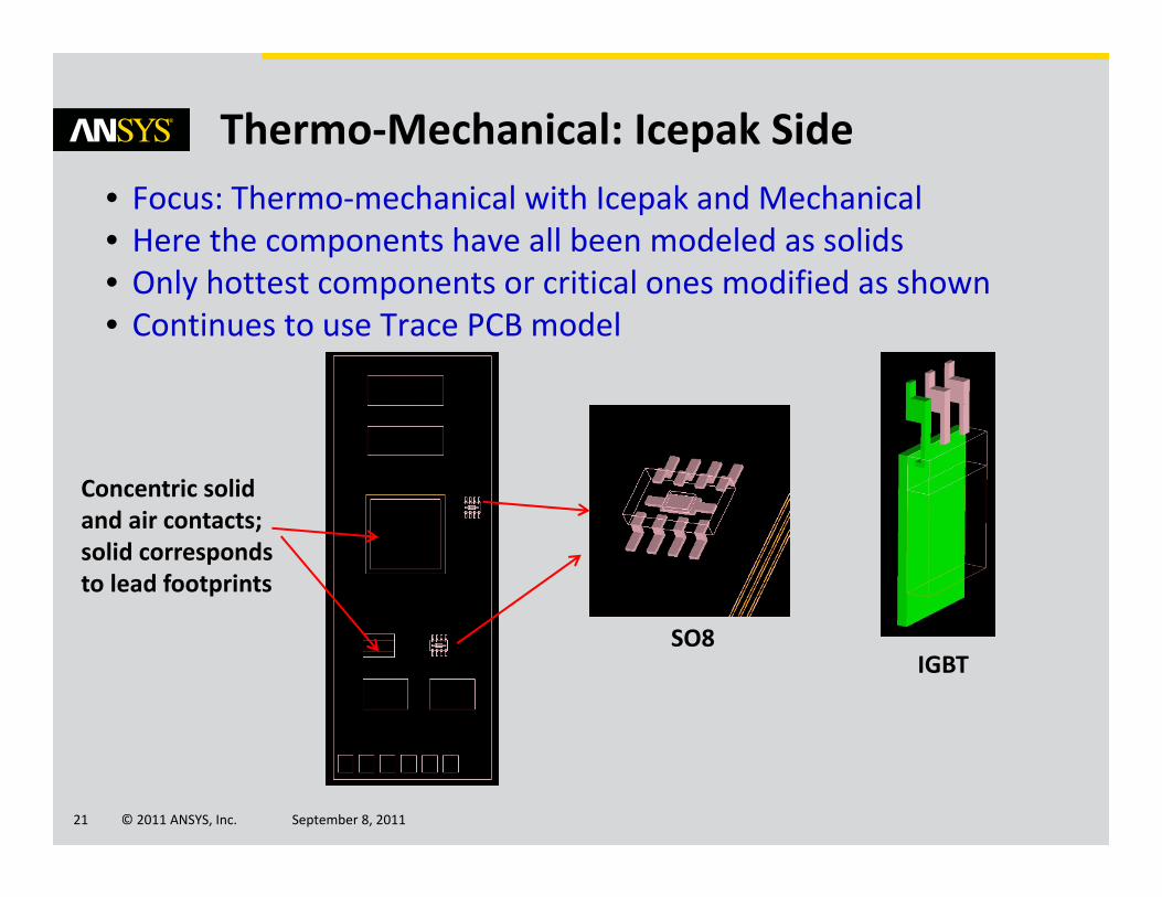
• Focus: Thermo‐mechanical with Icepak and Mechanical• Here the components have all been modeled as solids• Only hottest components or critical ones modified as shown• Continues to use Trace PCB model
Thermo‐Mechanical: Icepak Side
SO8IGBT
Concentric solid and air contacts; solid corresponds to lead footprints
© 2011 ANSYS, Inc. September 8, 201122
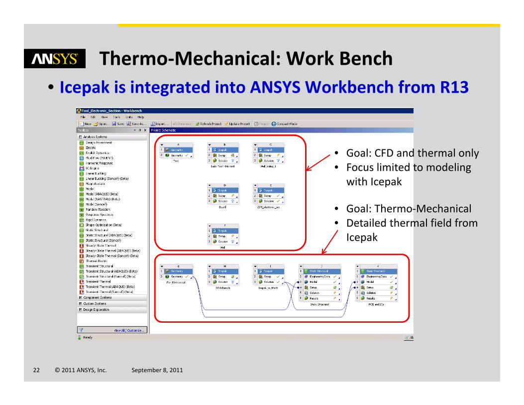
• Icepak is integrated into ANSYS Workbench from R13Thermo‐Mechanical: Work Bench
• Goal: CFD and thermal only• Focus limited to modeling with Icepak
• Goal: Thermo‐Mechanical• Detailed thermal field from Icepak
© 2011 ANSYS, Inc. September 8, 201123
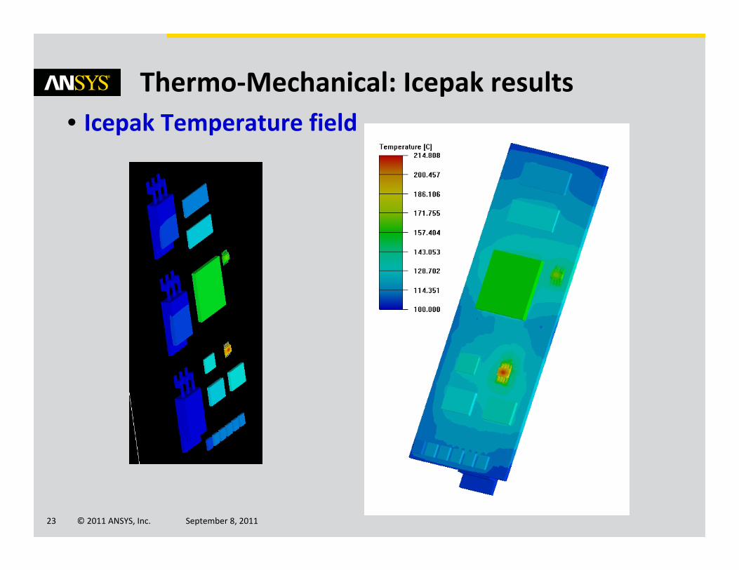
• Icepak Temperature fieldThermo‐Mechanical: Icepak results
© 2011 ANSYS, Inc. September 8, 201124
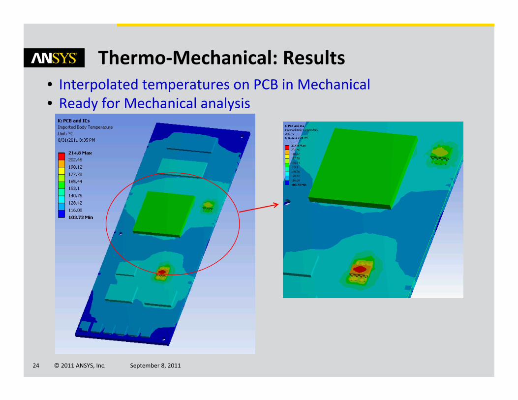
• Interpolated temperatures on PCB in Mechanical• Ready for Mechanical analysis
Thermo‐Mechanical: Results
© 2011 ANSYS, Inc. September 8, 201125
• Questions and CommentsThank you