Embed Size (px)
Citation preview
GOMACTech-05Government Microcircuit Applications
and Critical Technology Conference
FINALPROGRAM"Intelligent Technologies"
April 4 - 7, 2005
The Riviera HotelLas Vegas, Nevada
GOMACTech-05 ADVANCE PROGRAM
CONTENTS
• Welcome ............................................................................ 1• Registration ........................................................................ 3• Security Procedures........................................................... 3• GOMACTech Tutorials ....................................................... 3• Exhibition............................................................................ 5• Wednesday Evening Social ............................................... 5• Hotel Accommodations ...................................................... 6• Conference Contact ........................................................... 6• GOMACTech Paper Awards............................................... 6• GOMACTech Awards & AGED Service Recognition.......... 7• Rating Form Questionnaire ................................................ 7• Speakers’ Prep Room ........................................................ 7• CD-ROM Proceedings ....................................................... 7• Information Message Center.............................................. 8• Participating Government Organizations ........................... 8• GOMAC Web Site .............................................................. 8
GOMAC Session Breakdown• Plenary Session ............................................................... 91: Rad-Hard Electronics and Systems ................................... 102: Sensor Urban Warfare........................................................ 123: RF Power ........................................................................... 144: Rad-Hard Technology Roadmap ........................................ 165: Distributed Autonomous Sensor System............................ 186: Adaptive RF I...................................................................... 20• Poster Session.................................................................. 227: Array Technologies ............................................................. 268: TFAST ................................................................................ 279: Microwave CMOS .............................................................. 29
10: Advanced Packaging.......................................................... 3111: RF Photonics...................................................................... 3212: High-Performance Silicon................................................... 3313: Nanotechnology I ............................................................... 3414: Power Electronics............................................................... 3515: MEMS Circuits and Packaging I......................................... 3716: Nanotechnology II .............................................................. 3917: New Millennium Program ................................................... 4018: MEMS Circuits and Packaging II........................................ 4219: High-Performance Computing............................................ 4320: VISA I ................................................................................. 4521: Photonics I.......................................................................... 4722: Adaptive RF II..................................................................... 4923: VISA II ................................................................................ 5124: Photonics II......................................................................... 5225: Electronics for Extreme Environments I ............................. 5326: Wide-Bandgap Semiconductors I....................................... 5527: Rad-Hard by Design I......................................................... 5728: Electronics for Extreme Environments II ............................ 5929: Wide-Bandgap Semiconductors II...................................... 6130: Rad-Hard by Design II........................................................ 63
• GOMACTech-05 Steering Committee ............................. 64• GOMACTech-05 Program Committee ............................. 65• Conference Timetable ........................................Centerfold
WELCOME
The GOMACTech-05 Program Committee is pleased to welcomeyou to this year’s conference in Las Vegas, Nevada. GOMACTechstrives to be the Government’s pre-eminent conference for thereview of developments in microcircuit applications for govern-ment systems and has been utilized to announce major govern-ment microelectronics initiatives such as VHSIC, MIMIC, and others. GOMACTech was established in 1968 and is anUnclassified, Export-Controlled event that requires all participantsto be U.S. Citizens or legal U.S. Permanent Residents.
This year’s conference theme, “Intelligent Technologies,” recog-nizes that systems which can gather and analyze data as well asmake decisions autonomously in harsh unfriendly environmentsrequire a marriage of high-performance information-processingtechnologies with highly capable sensor technologies.
This year’s conference will follow a format that has proven verysuccessful in recent years in which both technical and topical ses-sions will be included. The technical sessions will consist ofpapers that are both contributed and solicited while the topicalsessions will consist of presentations that are focused on the workbeing performed within selected ongoing government-sponsoredprograms. Topical session themes this year include ArrayTechnologies, Technology for Frequency Agile DigitallySynthesized Transmitters (TFAST), Vertically Integrated SensorArrays (VISA), Sensors and Urban Warfare, The New MillenniumProgram, and Electronics for Extreme Environments.
On Tuesday morning the conference will formally begin with anexcellent Plenary Session. Mr. Pete Theisinger, Project Managerof the Mars Science Laboratory and the Mars Exploration Rovers,Jet Propulsion Laboratory (JPL), will present the Keynote Address“Rovers on Mars – The Technical Underpinnings”. In keeping withthe conference theme, the Jack Kilby Lecture Series will featureDr. James Hutchby of the Semiconductor Research Corporationdiscussing “Beyond Silicon,” Dr. Matthew Goodman of Telcordiapresenting insight into “FPGAs in DoD Systems – Benefits andChallenges,” and Prof. Linda Katehi of Purdue University will con-clude the series with “Three-Dimensional Circuits for Compact,Reconfigurable, and Multifunctional Systems.”
Prior to the formal opening of the conference, two tutorials will beoffered on Monday afternoon for which the cost is included as partof the conference registration fee. In the first tutorial,“Nanoelectronics,” four leaders in their respective areas will pro-vide overviews of recent progress in Nanotubes/Nanowires,Nano-magnetoelectronics, Nano-photonics, and Nanofabrication.The second tutorial, “Sensor Networks and Applications,” willreview the evolution of sensor-network research and address newopportunities resulting from advances in sensor computing, com-munication technologies, and challenges that must be met toimplement sensor networks.
The Plenary and Technical Paper Sessions are the major sourcesof formal information exchange that will occur at the conference.Other sources are provided through the Exhibition, which includesmajor IC manufacturers and commercial vendors of devices,equipment, systems, and services for nearly all facets of the elec-tronics business. The exhibition opens on Tuesday at noon and
1
runs through Wednesday at 4:00 pm. On Tuesday, following thelast technical paper session, representatives from various ICmanufacturers will present posters on efforts that support theRadiation-Hardened Technology Roadmaps. In addition, repre-sentatives from the Government will present posters on theirrespective capabilities in microelectronics technology develop-ment. Following the Poster Session, there will be an Exhibitors’Reception, sponsored by Northrop Grumman, where attendeescan mix in a relaxing atmosphere of food and good spirits. OnThursday, a Government Applications and Vision Session will beheld during lunch in which current and future directions of govern-ment-sponsored programs will be presented.
This strong technical program reflects the hard work of theGOMACTech-05 Technical Program Committee. The committeeaggressively sought out particular topics and areas for presenta-tions, and we think the quality of the conference this year will pos-itively reflect this effort. We appreciate your support and believethat GOMACTech-05 will be a rewarding experience.
Ingham A. Mack Sammy A. KayaliConference Chair Technical Program ChairOffice of Naval Research Jet Propulsion Laboratory
2
REGISTRATION
All sessions of GOMACTech-05 are being held here at the RivieraHotel in Las Vegas, Nevada. Both check-in and on-site registra-tion will take place in the hotel’s Convention Center Foyer.
Conference check-in and on-site registration hours:
Monday, 4 April – 10:00 am – 5:00 pmTuesday, 5 April – 7:00 am – 5:00 pmWednesday, 6 April – 7:00 am – 5:00 pmThursday, 7 April – 7:00 am – 5:00 pm
SECURITY PROCEDURES
The GOMACTech Conference is an Unclassified, Export-Controlled event that requires participants to be U.S. Citizens orlegal U.S. Permanent Residents. All registrants must provide proofof U.S. Citizenship or Permanent Resident status prior to beingpermitted entry into the conference. Additionally, a signed Non-Disclosure Statement will be required.
You may prove U.S. citizenship with any one of the following:U.S. PassportBirth Certificate AND valid government-issued photo IDNaturalization Certificate AND valid government-issued photo ID
The following are NOT proof of citizenship:Voter registration card Driver’s license
GOMACTech TUTORIALS
Two 4-hour tutorials of interest to the GOMACTech community area special feature of the conference. The tutorials are both beingheld on Monday, 4 April, 1:00 – 5:00 pm. There is no additional feefor the tutorials, but registrants must indicate their intention toattend on the registration form.
Tutorial 1: Nanotechnology Capri Room 101
Moderators: Chagaan Battar, IDA, Alexandria, VACliff Lau, IDA, Alexandria, VA
Nanotubes and Nanowires: An Overview in System DevelopmentM. Meyyappan, NASA Ames Research Center, Moffett Field, CA
Carbon nanotubes (CNTs) with their unique electronic propertiesand extraordinary mechanical properties have been the subject ofintensive research for logic, memory, actuator, and sensordevices. Recently, inorganic nanowires of silicon, germanium, andhigh-temperature oxides and nitrides have shown interestingcharacteristics to warrant consideration for the same applications.An overview of the growth, characterization, and applicationdevelopment in both mechanical systems will be given.
3
Nanoimprint Lithography: An Enabling Engine for Nanotechnologyand Next-Generation ICs
Stephen Y. Chou, Michael Austin, Neil Li, and Rich Yu, Princeton University, Princeton, NJ
Nanoimprint lithography (NIL) is a revolutionary method of nano-patterning that offers ultra-high resolution (sub 5 nm), highthroughput, and low cost – unmatchable by other existing lithog-raphy. NIL is regarded as one of 10 emerging technologies thatcan significantly change the world (MIT Technology Review) andhas been put on the International Roadmap for SemiconductorIndustry’s ITRS roadmap as one of the next generation of litho-graphies for IC manufacturing.
Spin-Transfer-Induced Excitations in Magnetic Nanostructures
W. H. Rippard, M. R. Pufall, S. Kaka, and T. J. SilvaNIST, Boulder, CO
Recent developments in spin-transfer-induced phenomena inmagnetic nanostructures will be discussed. More specifically, thiswill include an overview of high-speed-current-induced switchingand high-frequency (GHz) oscillations in magnetic “nanopillars”and “nanocontacts”.
Nanophotonics: New Opportunities for Integration of Lasers,Modulators, Filters, and Detectors for Data Communications andMicrofluidic Sensors
Axel SchererCaltech, Pasadena, CA
The emergence of silicon on insulator substrates, advanced crys-tal growth, and high-resolution fabrication techniques offers newopportunities for dense integration of optical devices. Theseopportunities, with a focus on filters, waveguides, resonators, andsurface plasmon devices, will be discussed.
Tutorial 2: Sensor Networks and ApplicationsCapri Room 102
Moderator: Sri Kumar, DARPA/IPTO, Arlington, VA
Dr. Sri KumarDARPA/IPTO, Arlington, VA
Advances in semiconductor and microelectromechanical (MEMS)technology have enabled a convergence of sensors, processing,and communications. This trend in hardware miniaturization andintegration of sensing, computing, and communication chips hasenabled a number of militarily-important applications. There is adesire to closely couple design of the network with the application,but the methods and tools to do this still remain a challenge. Thistutorial will review the evolution of sensor-network research andaddress new opportunities, resulting from advances in sensor,computing, and communication technologies, and challenges thatmust be met to implement sensor networks.
4
EXHIBITION
An exhibition comprised of commercial vendors exhibiting prod-ucts of interest to the GOMACTech community is an integral partof the conference. All attendees are reminded to visit theexhibitors when they have some free time. The Exhibit Hall islocated in the hotel’s Grand Ballroom E. Coffee breaks will beheld in the exhibit area when they coincide with the exhibition’shours of operation. On Tuesday evening an Exhibitors’ Reception,sponsored by the Northrop Grumman, where attendees can mix ina relaxing atmosphere of food and good spirits. Exhibition hoursare as follows:
Tuesday, 5 April 12:00 pm – 8:00 pmWednesday, 6 April 9:00 am – 4:00 pm
ExhibitorsAir Force Research LaboratoryAmkor Test ServicesAPIC Corp.ATK Mission ResearchAtmel Corp.BAE SystemsBoeing Phantom WorksCPU Technology, Inc.Discovery Semiconductors, Inc.Diversified TechnologiesDPA Components InternationalEDAptive Computing, Inc.HoneywellIBM Corp.JSI MicroelectronicsLSI Logic Corp.M/A – COMNational Reconnaissance OfficeNorthrop GrummanNxGen/US-SemiPeregrine SemiconductorSandia National LaboratoriesSilvaco InternationalSynopsys, Inc.
WEDNESDAY EVENING SOCIALThe Top of the Riv Ballroom on the 24th floor of the hotel’sMonaco Tower will be the site of this year’s Wednesday eveningdinner event. The Top of the Riv offers a spectacular view of thenight lights of Las Vegas. Dinner will be served at 7:00 pm followed by a top-flight Las Vegas entertainer. Tickets should bepurchased in advance along with your conference registration.Adults $ 25.
5
HOTEL ACCOMMODATIONSThe Riviera Hotel and Casino enjoys a legendary past as one ofthe first top-notch Las Vegas hotels in Nevada, known for its bigname entertainment and friendly hospitality, as well as its world-wide name recognition. Preparing for its Golden Anniversary in2005, the historic Riviera is one of the state’s premier destinationspots, offering the passion and excitement of nostalgic Las Vegas,combined with a modern-day, multi-million-dollar remodeling ofrooms and convention facilities, bringing the property up to parwith today’s mega-resort competition.
Over 2000 refurbished oversized rooms offer maximum comfortand breathtaking views of the glittering Las Vegas Strip with itswestern scenic panoramas. Each accommodation has beenattractively decorated.
GOMACTech has reserved a block of rooms at the special con-ference rates of $104 single, $109 double. These rates are exclu-sive of Clark County tax (currently 9%) and an energy surchargeof $3.50/night.
Reservations may be made by calling the hotel reservationsdepartment at 1-800-634-6753.
Not currently available, but anticipated before the time ofGOMACTech, all rooms will have wireless Internet capability at anadditional daily charge (expected to be $10/day).
CONFERENCE CONTACT
Anyone requiring additional information about GOMACTechshould contact the Conference Coordinator, Ralph Nadell,GOMACTech, 411 Lafayette Street, Suite 201, New York, NY10003 (212/460-8090 x203), [email protected].
GOMACTech ‘04 PAPER AWARDS
Paper awards based on audience evaluations from GOMACTech-04 will include the George Abraham Outstanding Paper Award anda Meritorious Paper Award to the runner-up. Presentation of thesewell-deserved awards will be made at the Plenary Session onTuesday morning in Grande Ballroom C/D. The GOMACTech-04winners are:
The George Abraham Outstanding Paper Award (7.1)J. W. Ward, M. Meinhold, T. R. Bengston, and G. F. CarletonNantero, Inc., Woburn, MA“Large-Scale Integration of Single-Walled Carbon-Nanotube(CNT) Nonvolatile RAM”
Meritorious Paper Award (18.7)F. AyaziGeorgia Institute of Technology, Atlanta, GA“Nano-Precision Integrated Electromechanical Filters forUHF Communications”
6
AGED SERVICE RECOGNITION
The following individuals will be recognized for their contributionsto the DoD through their service on the Advisory Group onElectron Devices:
Peter Asbeck Conilee KirkpatrickJohn Brock Charles KrummJon Christensen David MyersJames Clary Joseph SaloomBarry Dunbridge William TennantBarry Gilbert Richard WilliamsonMay Hibbs-Brenner Debbie WilsonWilliam Howard Andrew Yang
RATING FORM / QUESTIONNAIRE
Do not forget to vote for your favorite presentation this year beforeyou leave the conference. A rating form/questionnaire is beinghanded out at conference check-in. To encourage the submissionof forms, all attendees who hand in a completed form at the reg-istration desk will be given a USB laptop-computer light.
SPEAKERS’ PREP ROOM
Capri Room 109 is designated as a speakers’ preparation roomand will be available during the hours the conference registrationdesk is open. Speakers are encouraged to use the Capri 109facilities to ensure compatibility with the meeting’s A/V equipment.Speakers having difficulties should request at the conference reg-istration desk to see an A/V operator. Speakers are also asked tobe at their assigned presentation room 30 minutes before the ses-sions begins to meet with their session chair. An A/V operator willbe assigned to each technical session room.
CD-ROM PROCEEDINGS
The first volume of the GOMACTech CD-ROM Proceedings, containing searchable, condensed versions of submitted paperspresented at the conference will be distributed to all registrants.Additional copies of the CD-ROM can be purchased at the conference at a cost of $40.00 per CD.
Previously published as the GOMAC Digest of Technical Papers,Volumes I – XXVIII, this publication is the only record of the con-ference. Previous GOMAC digests will, upon request, be madeavailable to qualified Defense Technical Information Center(DTIC) users. Please call 1-800-225-3842 for bound or microfichecopies. Past Digests can be ordered by calling the above numberand identifying the following accession numbers (please note thatGOMAC was not held in the calendar year of 1995):
7
GOMAC-84 B113271 -86 B107186 -87 B119187
-88 B129239 -89 B138550 -90 B150254
-91 B160081 -92 B169396 -93 B177761
-94 B195015 -96 B212362 -97 B222171
-98 B235088 -99 B242763 -00 B254138
-01 B264749 -02 B275146 -03 M201604
-04 M201663
INFORMATION / MESSAGE CENTER
The Information/Message Center will be located adjacent to theGOMACTech Registration Desk located in the Conference CenterFoyer. The message center telephone number for incoming callsis 702/734-5110. Callers should ask to be transferred to theGOMACTech Registration Desk.
PARTICIPATING GOVERNMENT ORGANIZATIONS
Participating Government Organizations of GOMACTech-05 include:Department of Defense (Army, Navy, Air Force) ... National Aeronautics andSpace Administration ... Department of Commerce (National Institute ofStandards and Technology) ... National Security Agency ... Department ofEnergy (Sandia National Laboratories) ... Defense Logistics Agency ...Department of Health and Human Services ... Defense Threat ReductionAgency ... Defense Advanced Research Projects Agency ... CentralIntelligence Agency ... National Reconnaissance Office
GOMAC WEB SITE
Information on GOMACTech may be obtained through its Web siteat www.gomactech.net.
8
TUESDAY, 5 APRIL
PLENARY SESSIONTuesday, April 5 / 8:30 am – 12:00 pm / Grande Ballroom C/D
Opening Remarks (8:30–8:45)
Ingham Mack, GOMACTech-05 General ChairOffice of Naval Research, Arlington, VA
GOMACTech Awards and AGED Service (8:45–9:00)Recognition
Keynote Address (9:00–10:00)
Mr. Peter TheisingerManager, Mars Science Laboratory ProjectJet Propulsion Laboratory, Pasadena, CA“Rovers on Mars – The Technical Underpinnings”
BREAK (10:00–10:30)
Jack S. Kilby Lecture Series (10:30–12:00)
Dr. James HutchbySRC, Research Triangle Park, NC“Beyond Silicon”
Dr. Matthew S. GoodmanChief Scientist and Telcordia FellowTelcordia Technologies, Red Bank, NJ“FPGAs in DoD Systems – Benefits and Challenges”
Prof. Linda KatehiDean of EngineeringPurdue University, West Lafayette, IN“Three-Dimensional Circuits for Compact,Reconfigurable, and Multifunctional Systems”
LUNCH (12:00–1:30)
9
Session 1
RAD-HARD ELECTRONICS AND SYSTEMS
Tuesday, April 5 / 1:30 – 3:30 pm / Grande Ballroom C
Chair: Lew CohnDTRA, Fort Belvoir, MD
Co-Chair: Ken LabelNASA–GSPC, Greenbelt, MD
1.1: Silicon-Carbide Rad-Hard Power Semiconductors (1:30)
C. SevertAFRL/PRPE, Wright-Patterson AFB, OH
This presentation will define silicon carbide power devices that have beensubjected to radiation tests and present characterization data prior to andsubsequent to various levels and types of radiation. Conclusions concern-ing the general radiation tolerance and specific device capabilities whileoperating in a radiation environment will be made.
1.2: A Rad-Hard 128K × 36 SRAM for Space (1:50)Applications
S. Doyle, T. Hoang, E. Maher, J. GilliamBAE SYSTEMS, Manassas, VA
A new high-performance 128K × 36 SRAM is being developed in 0.15-µmRH15 technology for use in space and other strategic rad-hard applications.For the first time, a synchronous architecture has been selected, allowingusers greater flexibility and compatibility with commercial pipelined syn-chronous, late write, and burst SRAMs. By using advanced RHBD tech-niques, 200-MHz operation will support 1x cycle time when used as L2Cache with the RAD750 microprocessor.
1.3: 150-nm Rad-Hard SOI-Structured ASIC Family (2:10)
D. Kagey, J. Hobbs, J. CulpHoneywell SSEC, Minneapolis, MN
D. HoltLightspeed, Santa Clara, CA
Honeywell is leveraging its 150-nm assured rad-hard SOI technology todevelop a structured ASIC solution to the Hi-Rel Space requirements forTID and SEU hardened flight units. The structured ASIC approach will cuttraditional NRE costs by a factor of 5, while keeping delivery cycles forASICs with more than a million gates to 12–15 weeks.
1.4: A Rad-Hard 0.25-µm Mixed-Signal CMOS Technologyfor Read-Out ICs and Extreme Temperature (2:30)Applications
M. S. Polavarapu, J. Ishii, M. Girmay, E. ChanBAE SYSTEMS, Manassas, VA
A rad-hard 0.25-µm mixed-signal CMOS technology, featuring shallowtrench isolation (STI), dual-work-function gate electrodes, capacitors, andresistors, will be described. The results demonstrate suitability for read-outintegrated circuits (ROICs) and other extreme temperature applications.
10
1.5: A 0.15-µm Rad-Hard Anti-Fuse Field-Programmable Gate-Array Technology (2:50)
D. Patel, L. Rockett, S. Danziger, B. SujlanaBAE SYSTEMS, Manassas, VA
There is a growing need for high-density rad-hard field-programmable gatearrays (FPGAs) that meet the needs of military and space applications. BAESYSTEMS, in partnership with the DoD community, is currently moderniz-ing its process facility located in Manassas, Virginia, to support a strategi-cally rad-hard 0.15-µm bulk CMOS process technology. This paperdescribes the features and data of a 0.15-µm rad-hard anti-fuse FPGA.
1.6: Implementing Next-Generation Rad-Hard ASICs (3:10)
J. AveryHoneywell, Plymouth, MN
Honeywell is introducing a 150-nm design and manufacturing capability toproduce radiation-tolerant and rad-hard ASICs with nearly 15 million gates.The initial challenge in developing rad-hard ICs is in the front-end design. Avery deep submicron multimillion-gate ASIC requires a fundamentally different approach than traditional methods. This paper will address adesign flow and infrastructure model Honeywell has developed to manageVDSM design complexity.
BREAK (3:30–3:40)
11
Session 2
SENSOR URBAN WARFARETuesday, April 5 / 1:30 – 3:10 pm / Grande Ballroom D
Chair: Kathleen A. GriggsPuritan Research Corp., Vienna, VA
2.1: The Promise and Challenge of Vision-Based Obstacle Avoidance for Unmanned Flight in Urban (1:30)Environments
J. E. CorbanGuided Systems Technologies, Inc., McDonough, GA
A. R. Tannenbaum, A. J. Calise, E. N. JohnsonGeorgia Institute of Technology, Atlanta, GA
Autonomous operation of unmanned flight systems in urban environmentsis precluded by the immature state of obstacle avoidance technology.Recent advances in image processing hint at the potential for image-basedobstacle avoidance, but will require integration with advanced micro-electronics to achieve practical real-time implementation. The promise andchallenge will be discussed, and collaboration in implementation sought.
2.2: Ground-Attack Warning System (1:50)
I. Agurok, T. Jannson, G. SavantPhysical Optics Corp., Torrance, CA
J. McCalmontAFRL, Wright-Patterson AFB, OH
Physical Optics Corporation will present its development of the GroundAttack Warning System (GAWS). The GAWS will be mounted on armoredvehicles and operates in urban battlefield environments to detect the launchof RPG and TOW missiles and track them in flight.
2.3: Sentient Environments Using Video-Based Wide-Area Tracking and Immersive Visualizations (2:10)
M. Aggarwal, T. Germano, A. Arpa, S. SamarasekeraSarnoff Corp., Princeton, NJ
A sentient system that combines comprehensive detection and tracking ofall moving objects and immersive visualization of a cluttered and crowdedenvironment using a network of stereo cameras will be presented. Smartprocessing is used to analyze stereo video streams to detect and track allmoving objects in cluttered urban environments. The system is designedspecifically to monitor moving people within a localized environment suchas an office building, terminal, or other enclosed site.
2.4: Intelligent Photonic Sensors for Urban Warfare (2:30)
R. Dutt, J. ChanAPIC Corp., Culver City, CA
APIC has been pursuing SOI system-on-a-chip technology because of itscapability of incorporating both photonics and electronics circuits on onechip. The result of a very-low-loss SOI waveguide and an intelligent SOIsensor that can be used for chemical, biological, or simply as a pressuresensor will be presented. Finally, an intelligent dual-band imager for urbanwarfare will be described. These miniaturized sensor systems with on-chipprocessing and communication capability could be key components for distributed intrusion alert systems.
12
2.5: Real-Time Stereo-Based Obstacle Detection for UAV Threat Avoidance (2:50)
J. Byrne, M. Cosgrove, R. MehraScientific Systems Company, Inc., Woburn, MA
A system for UAV obstacle detection based on Sarnoff Corp’s Acadia Ivision processor for 23-Hz 640 x 480 binocular stereo and 10-Hz mincut-based recursive bipartition of an affinity graph on embedded hardware willbe described. Simulation, indoor, outdoor, and flight-experiment results willbe given.
BREAK (3:10–3:40)
13
Session 3
RF POWERTuesday, April 5 / 1:30 – 3:10 pm / Grande Ballroom G
Chair: Denis C. WebbNaval Research Laboratory, Washington, DC
3.1: High-Frequency Power Metamorphic HEMT (1:30)
C. S. Whelan, K. Herrick, J. Laroche, K. W. BrownRaytheon, Andover, MA
By tailoring the devices material, geometry, and processing, device design-ers have fabricated a state-of-the-art high-frequency metamorphic HEMTdevice with a Gmax of 12 dB, a power density of 360 mW/mm, and PAEsexceeding 30% at 95 GHz. This device had been utilized to create a rangeof W-band amplifiers with excellent performance, including a 266-mW PAoperating at 90 GHz.
3.2: 56-W SiC MESFET Transistors with a PAE > 50% for L-Band Applications (1:50)
B. Luo, P. Chen, A. Higgins, H. Finlay Rockwell Scientific, Thousand Oaks, CA
A large gate periphery SiC MESFET has been designed and fabricated. Apeak output power of 56 W and a PAE of 53% was measured from 30-mmsingle-die packaged transistors. The device dc characterization, frequencyresponse, and statistical analysis will be presented.
3.3: The Design of Low-Cost 4- and 6-W MMIC High-PowerAmplifiers for Ka-Band Modules (2:10)
M. R. Lyons, C. D. Grondahl, S. M. DaoudU.S. Monolithics, Chandler, AZ
Two Ka-band power-amplifier MMICs, 4 and 6 W, with high power densityand gain will be presented. Each amplifier was designed by using a five-stage topology to demonstrate over 30 dB of gain. The 4-W design exhibit-ed a peak saturated output power of 37.2 dBm and a chip output powerdensity of 532 mW/mm2. This is the highest recorded power density for aKa-band power-amplifier design to date. The high gain and power densityof these designs make them ideal for low-cost Ka-band transmit systems.
3.4: A V-Band GaAs PHEMT Power Amplifier for Crosslink Applications (2:30)
K-L. Ngo Wah, Y. C. Chou, J. Goel, R. GrundbacherNorthrop Grumman, Redondo Beach, CA
A GaAs PHEMT MMIC power amplifier for crosslink satellite applicationsfrom 59 to 63 GHz will be presented. This MMIC demonstrates an outputpower performance of greater than 30.7 dBm on a full MMIC (greater than28.5 dBm on half MMIC) and leads to the demonstration of a solid-statepower amplifier (SSPA) module with a output power of 12.8 W at V-bandusing a low-loss combining technique.
14
3.5: High-Voltage MESFET Technology for MMIC (2:50)Applications
T. A. Winslow, D. ConwayTycoelectronics, Roanoke, VA
High-voltage MESFET technology has been developed to address theneeds of military radar system integrators, who require low-cost high-yieldhigh-power-density power amplifiers. The high-voltage MESFET process is an extension of an existing and very mature MSAG MESFET process.24-V high-power MMICs have been developed and have demonstratedexcellent performance.
BREAK (3:10–3:40)
15
Session 4
RAD-HARD TECHNOLOGY ROADMAPSTuesday, April 5 / 3:40–5:10 pm / Grande Ballroom C
(Note: These papers are also included in the Poster Session)
Chair: Lew CohnDTRA, Fort Belvoir, MD
Co-Chair: Ken LabelNASA–GSPC, Greenbelt, MD
4.1: BAE SYSTEMS Rad-Hard Microelectronics Technology Roadmap (3:40)
L. Rockett, N. Haddad, M. Polavarapu, T. BachBAE SYSTEMS, Manassas, VA
BAE SYSTEMS, in partnership with the DoD, is completing foundry mod-ernization to be rad-hard 150-nm CMOS technology production ready by2Q ’05. The rad-hard technology roadmap identifies the technology exten-sions being pursued to advance their rad-hard technology capabilitiesbeyond the 150-nm technology node to closely track the technology capa-bilities offered by commercial foundries.
4.2: Peregrine Semiconductor Technology Roadmap (3:50)
C. TabbertPeregrine Semiconductor, Albuquerque, NM
Peregrine Semiconductor will present technology and product roadmapssupporting highly integrated RF and photonic products for space applica-tions. Highlighted during this presentation will be recent advances in inte-grated GPS receiver technology and transmit-receiver module integrationfor phased-array antenna applications along with new RF products extend-ing RF CMOS into Ku-Band RF applications.
4.3: Roadmap to 150-nm Rad-Hard Semiconductor (4:00)Products
G. Kirchner and J. HobbsHoneywell Defense & Space Electronics Systems
Honeywell has developed radiation-tolerant 150-nm semiconductor tech-nology and rad-hard capability before the end of 2005. Near-future productsbased on 150-nm technology include 15-million-gate ASICs, 16MB SRAMs,1MB MRAMS, and high-speed SerDes.
4.4: Title III Microelectronics Programs (4:10)
E. Pohlenz and B. HagertyAFRL (Title III), Wright-Patterson AFB, OH
P. HastingsNorthrop Grumman Information Technology, Fairborn, OH
All of the Title III programs that are pertinent to military microelectronics,including programs such as CAPEX and Space Microprocessors as well asother Title III programs focused on space, will be discussed.
16
4.5: Northrop Grumman Rad-Hard Technology (4:20)Overview
D. Adams, M. FitzpatrickNorthrop Grumman Corp., Linthicum, MD
A broad range of mixed-signal, power, and nonvolatile memory products forspace and avionics applications that are produced at the NorthropGrumman Corporation (NGC) Advanced Technology Center in Baltimore,Maryland, will be described.
4.6: The Continued Evolution of Re-Configurable FPGAs for Military and Space Strategic Applications
H. Bogrow, J. Fabula, J. MooreXilinx, Albuquerque, NM
Present and future military and space applications continue to demand everincreasing performance, density, and above all flexibility from FPGAs. TheVirtex families of re-configurable FPGAs provide the technology to meetthese demands. This paper will focus mainly on Xilinx’s currently availableVirtex solutions, while possibly also discussing Xilinx’s future developmentefforts.
4.7: Aeroflex’s Roadmap for the Development of Rad-Hard ICs Using Commercial Foundries (4:30)
D. WilkinAeroflex, Inc., Colorado Springs, CO
Aeroflex Colorado Springs will present their roadmap for the continueddevelopment of rad-hard integrated circuits using commercial waferfoundries. Products built on 0.6-, 0.25-, and 0.18-µm CMOS commercial silicon using a combination of design hardness and/or co-processing tech-niques will be summarized.
4.8: Rad-Hard Technology Roadmap for Microelectronics and Space Computers (4:40)
D. R. Czajkowski, D. J. StrobelSpace Micro, Inc., San Diego, CA
The ability to leverage advanced commercial COTS microelectronics is crit-ical to providing warfighters capability. Space Micro’s technology roadmap,products, and techniques, which enable use of COTS in a radiation envi-ronment, will be described.
4.9: Actel Corp.’s Technology Roadmap (4:50)
B. Cronquist, C Clardy, K. Oneill, T. FarinaroActel Corp., Mountain View, CA
Actel Corporation’s product roadmap for high-reliability applications will bepresented. Both the non-volatile one-time programmable (OTP) FPGA andthe non-volatile re-programmable FPGA roadmap will be discussed.Commercial, MIL-TEMP, rad-tolerant, and rad-hard efforts will be described.Special mention will be given to the definition, content, and schedule for theradiation-tolerant non-volatile re-programmable field-programmable gate-array (RTNVRFPGA) product family. The Actel packaging roadmap for high-reliability applications will also be presented.
17
WITHDRAWN
Session 5
DISTRIBUTED AUTONOMOUS SENSOR SYSTEMS
Tuesday, April 5 / 3:40 – 5:20 pm / Grande Ballroom D
Chair: Jill P. DahlburgNaval Research Laboratory, Washington, DC
Co-Chair: Kathleen A. GriggsPuritan Research Corp., Vienna, VA
5.1: Physicomimetics Positioning Methodology for (3:40)Distributed Autonomous Systems
M. W. M. Spears, D. F. SpearsUniversity of Wyoming, Laramie, WO
A framework called “physicomimetics” that provides distributed control oflarge collections of mobile vehicles will be described. This framework allowshundreds of vehicles to self-organize into sensor networks. The practicalityof this approach on the “chemical-plume tracing” task, which traces a toxicplume to its source emitter, will be discussed.
5.2: Visualization for Volumetric Control in a Mobile Environment (4:00)
D. P. SchisselGeneral Atomics, San Diego, CA
A mobile sensor suite with advanced volumetric visualization and displaytechnology can provide rapidly deployable surveillance and security forhigh-value assets or at suspected areas of enemy activity. This presenta-tion will discuss the technical state of the art as well as give results from thedemonstration of a first prototype.
5.3: Efficient Broadband RF Energy Harvesting for Wireless Sensors (4:20)
R. Zane, Z. PopovicUniversity of Colorado, Boulder, CO
A solution for high-efficiency broadband RF power delivery to miniaturewireless sensors, thus alleviating distributed sensor networks from powerwires or periodic battery replacement, will be demonstrated. The approachis based on broadband rectenna design and high-efficiency power-processing circuitry.
5.4: Embedded-Gas-Sensor System-on-Chip (4:40)Characterization System
Y. Afridi, A. Hefner, C. Ellenwood, R. CavicchiNIST, Gaithersburg, MD
A characterization system for evaluating critical functions of a micro-hotplate-based embedded gas sensor for system-on-a-chip applications willbe presented. The system uses a virtual instrument interface to controlparts-per-billion (ppb) gas-concentration levels and microhotplate tempera-ture-controlled registers and acquires temperature- and gas-sensor datathrough an on-chip analog-to-digital converter.
18
5.5: Robust Fiber-Optic Chemical/Gas-Sensing (5:00)Systems
H. Xia, K-Li DengGE Global Research, Niskayuna, NY
This paper demonstrates that chemical sensing can be implemented basedon bared FBGs and LPGs without etching, cladding, or chemical-activecoating. The results, for the first time, have disclosed that the chemicalsensing based on FBG is a one-step process due to chemical atom diffu-sion effect. The developed sensing systems are robust and compatible toexisting fiber-optic devices.
19
Session 6
ADAPTIVE RF ITuesday, April 5 / 3:40 – 5:20 pm / Grande Ballroom G
Chair: Eric D. AdlerArmy Research Laboratory, Adelphi, MD
Co-Chair: William D. PalmerArmy Research Laboratory, Adelphi, MD
6.1: Miniature Tunable Combline Filters (3:40)
S. Mehta, P. Petre, J. FoschaarHRL Labs, Malibu, CA
HRL Laboratories’ progress in developing state-of-the-art extremely minia-ture, tunable combline filters for the C, X, and Ku-bands will be reported.These filters are essential components for ONR’s Advanced MultifunctionRF System Concept (AMRF-C). The salient filter features are small size,low insertion loss, high tunability, and fast response time.
6.2: RF on Flex Panel for X-Band Phased Arrays (4:00)
A. Jacomb-Hood, R. Melcher, E. Lier, E. TalleyLM CSS, Newtown, PA
T. Destefano, P. Kraft, N. Fardella, V. OzunaLM MS2, Moorestown, NJ
A passive X-band phased-array panel using RF-on-flex interconnect to minimize mass and cost has been fabricated and tested. The panel wasassembled using an industry-standard automated assembly line. State-of-the-art panel mass was demonstrated. The measured antenna perfor-mance is in reasonable agreement with the predicted performance.
6.3: Packaging and Transitions for Intelligent RF (4:20)Microsystems
K. HerrickRaytheon, Andover, MA
A. MargomenosEMAG Technologies, Ann Arbor, MI
R. LahijiPurdue University, West Lafayette, IN
Y. LeeEMAG Technologies, Ann Arbor, MI
By integrating a university RF MEMS packaging process with an industryIII-V standard, a manufacturable process has been developed which inte-grates FETs, RF MEMS, vertical RF transitions, and thermocompressionbonded packaging on GaAs substrates. Significant benchmarks in thisdevelopment include individual transition and wafer bonding results.
20
6.4: Low-Temperature Wafer-Level Packaging for RF MEMS Switches (4:40)
P. Chang-Chien, K. Tornquist, M. Truong, C. GeigerNorthrop Grumman Space Technology, Redondo Beach, CA
A low-temperature high-yield wafer-level-packaging (WLP) technique hasbeen developed and demonstrated. Data obtained from packaged MEMSswitches shows this WLP technique produces close to 100% cavity bond-ing yield and a very high packaged device yield. The encapsulated switchis accessed through low-loss RF vias from the backside of the package,which is only 100-µm thick. Furthermore, this technology is compatible withNGSTs standard 100-mm MMIC fabrication processes, making packagingMMIC-integrated MEMS devices with this WLP technology possible.
6.5: High-Efficiency RF Class E Power Amplifiers for Unattended Ground Sensor Applications (5:00)
J. D. Popp, J. F. Rowland, A. H. YangSPAWAR System Center San Diego, San Diego, CA
D. Y. C. LieSYS Technologies, San Diego, CA
This paper investigates high-efficiency RF Class E power-amplifier technol-ogy for unattended ground sensor systems. Results of designs using COTStechnology and IBM SiGe 7HP technology operating in the 300-MHz and 2.4-GHz bands will be presented. These designs demonstrate 3x improve-ments in power efficiency over available technology.
21
Interactive Session
POSTER SESSIONTuesday, April 6 / 5:20 – 6:30 pm / Grande Ballroom H
Chair: Lew CohenDTRA, Ft. Belvoir, MD
Government Laboratories
P.1: AFRL Mixed-Signal Design Center
V. J. Patel, H. S. Axtell, C. L. A. CernyAFRL/SND, Wright-Patterson AFB, OH
For many years, receivers have taken advantage of the III-V technologiesfor performance. However, these technologies and system packaging haveproven to be expensive and challenging to integrate. Also, the difficulty ofachieving first-pass fabrication success in III-V and in silicon technologiescompounds the problem of cost. Therefore, AFRL and DARPA initiatedefforts to reduce the cost of these receiver systems by evaluating anddemonstrating advanced silicon processes. In the attempt to achieve first-pass success, DARPA funded the NeoCAD effort that allowed both industryand universities to put forth ideas and develop new electronic-design-automation tools for RF and analog.
P.2: Defense Microelectronics Activity Capabilities
D. PentrackDefense Microelectronics Activity, McClellan, CA
DMEA provides the DoD with a variety of microelectronics design, fabrica-tion, and test services. Digital, analog, mixed-signal, RF, and EEPROMdevices are fabricated in a true flexible foundry using a variety of licensedprocesses. DMEA thereby assures a continued source of supply for 5 V andrad-hard technologies.
P.3: Radiation-Tolerant Microelectronics Developments at NAVSEA Crane
J. McKamey, D. Platteter, S. ClarkNAVSEA Crane, Crane, IN
Current work includes nuclear hardening and design of guidance systemelectronics for the Navy’s Trident II missile system along with radiationeffects research and development for the Defense Threat ReductionAgency.
P.4: Air Force Research Laboratory
C. GordonAFRL/VSSE, Kirtland AFB, NM
Advances in microelectronics are revolutionizing defense capabilities, withspace-based surveillance, communications, and navigation as prime exam-ples. In search of transformational military space capabilities, the Air ForceResearch Laboratory’s Space Vehicles Directorate is focusing on reconfig-urability, very high performance, and design hardening as a foundation foraffordable, sustainable spacecraft electronics.
22
WITHDRAWN
P.5: NRL Electronics S&T Program
A. Campbell, G. M. BorsukNRL, Washington, DC
NRL conducts an in-house multi-disciplinary research program thataddresses six thrust areas: solid-state electronics, nanoelectronics, plasmascience and technology, power electronics, vacuum electronics, and elec-tro-optics science and technology. A brief overview of the key researchopportunities being addressed in each of these thrusts will be presented.
P.6: The NASA Electronic Parts and Packaging (NEPP) Program: Roadmap for NASA’s Radiation Effects on and Reliability of Electronics Efforts
K. A. LaBel, M. J. SampsonNASA/GSFC, Greenbelt, MD
C. E. BarnesJet Propulsion Laboratory, Pasadena, CA
The NEPP Program is responsible for developing the plans for and leadingthe research on reliability and radiation response in the space and aero-nautics environments. Presented herein are the current NASA tasks as wellas a consideration of future research areas.
P.7: The Sandia National Laboratories Microelectronics Program
K. K. Ma, F. W Sexton, P. E. DoddSandia National Laboratories, Albuquerque, New Mexico
The current status of the Sandia National Laboratories Radiation-HardenedMicroelectronics Program wii be described. The influence of many factorson the program’s direction, including the acceptance of using commercialfield-programmable gate arrays, single-event transient effects on ultra-deep-submicron silicon technologies, hardened-by-design methodology,and trends in commercial microelectronic industry, will be discussed.
P.8: The NIST Workshop on Reliability Issues in Nano-Materials
R. R. Keller, D.T. ReadNIST, Boulder, CO
The introduction of nanomaterials into current and future technologiesopens up an entirely new suite of both materials science and measurementscience challenges. Effects of dimensional scaling play a stronger role inthe reliability of nanomaterials than in any other materials known to date.Surfaces and interfaces can easily dominate and change behavior andproperties known to develop in bulk materials of the same chemical com-position. As such, one cannot simply extrapolate what is now known aboutbulk material behavior to the nanoscale and expect to predict the structureor properties accurately. In order to address many of these concerns, NISThosted a workshop entitled “Reliability Issues in Nanomaterials,” held17–19 August, 2004 in Boulder, Colorado, to discuss research issues andmeasurement-related barriers that affect the reliability of extremely fine-scale materials.
23
P.9: Reliability Construction Analysis Anticipating the Next DMS Train Wreck: How to Evaluate Ultra-Submicron-Feature-Size IC Reliability
G. GauglerDMEA, Sacramento, CA
This new work uses EBSD as a key analysis method for predicting lifetimeexpectations of COTS integrated circuits when used in a military environ-ment. This work focuses on electromigration effects as significant overother effects that are receiving different attention.
Industry Roadmaps
P.10: BAE SYSTEMS’s Rad-Hard Microelectronics Technology(4.1) Roadmap
L. Rockett, N. Haddad, M. Polavarapu, T. BachBAE SYSTEMS, Manassas, VA
BAE SYSTEMS, in partnership with the DoD, is completing foundry mod-ernization to be rad-hard 150-nm CMOS technology production ready by2Q ’05. The rad-hard technology roadmap identifies the technology exten-sions being pursued to advance their rad-hard technology capabilitiesbeyond the 150-nm technology node to closely track the technology capa-bilities offered by commercial foundries.
P.11: Peregrine Semiconductor’s Technology (4.2) Roadmap
C. TabbertPeregrine Semiconductor, Albuquerque, NM
Peregrine Semiconductor will present technology and product roadmapssupporting highly integrated RF and photonic products for space applica-tions. Highlighted during this presentation will be recent advances in inte-grated GPS receiver technology and transmit-receiver module integrationfor phased-array antenna applications along with new RF products extend-ing RF CMOS into Ku-Band RF applications.
P.12: Roadmap to 150-nm Rad-Hard Semiconductor (4.3) Products
G. Kirchner and J. HobbsHoneywell Defense & Space Electronics Systems
Honeywell has developed radiation-tolerant 150-nm semiconductor tech-nology and rad-hard capability before the end of 2005. Near-future productsbased on 150-nm technology include 15-million-gate ASICs, 16MB SRAMs,1MB MRAMS, and high-speed SerDes.
P.13: Title III Microelectronics Programs(4.4)
P. HastingsNorthrop Grumman Information Technology, Fairborn, OH
All of the Title III programs that are pertinent to military microelectronics,including programs such as CAPEX and Space Microprocessors as well asother Title III programs focused on space, will be discussed.
24
P.14: Northrop Grumman’s Rad-Hard Technology (4.5) Overview
D. Adams, M. FitzpatrickNorthrop Grumman Corp., Linthicum, MD
A broad range of mixed-signal, power, and nonvolatile memory products forspace and avionics applications that are produced at the NorthropGrumman Corporation (NGC) Advanced Technology Center in Baltimore,Maryland, will be described.
P.15: The Continued Evolution of Re-Configurable FPGAs (4.6) for Military and Space Strategic Applications
H. Bogrow, J. Fabula, J. MooreXilinx, Albuquerque, NM
Present and future military and space applications continue to demand everincreasing performance, density, and above all flexibility from FPGAs. TheVirtex families of re-configurable FPGAs provide the technology to meetthese demands. This paper will focus mainly on Xilinx’s currently availableVirtex solutions, while possibly also discussing Xilinx’s future developmentefforts.
P.16: Aeroflex’s Roadmap for the Development of Rad-Hard (4.7) ICs Using Commercial Foundries
D. WilkinAeroflex, Inc., Colorado Springs, CO
Aeroflex Colorado Springs will present their roadmap for the continueddevelopment of rad-hard integrated circuits using commercial waferfoundries. Products built on 0.6-, 0.25-, and 0.18-µm CMOS commercial silicon using a combination of design hardness and/or co-processing tech-niques will be summarized.
P.17: Rad-Hard Technology Roadmap for Microelectronics (4.8) and Space Computers
D. R. Czajkowski, D. J. StrobelSpace Micro, Inc., San Diego, CA
The ability to leverage advanced commercial COTS microelectronics is crit-ical to providing warfighters capability. Space Micro’s technology roadmap,products, and techniques, which enable use of COTS in a radiation envi-ronment, will be described.
P.18: Actel Corp.’s Technology Roadmap(4.9)
B. Cronquist, C Clardy, K. Oneill, T. FarinaroActel Corp., Mountain View, CA
Actel Corporation’s product roadmap for high-reliability applications will bepresented. Both the non-volatile one-time programmable (OTP) FPGA andthe non-volatile re-programmable FPGA roadmap will be discussed.Commercial, MIL-TEMP, rad-tolerant, and rad-hard efforts will be described.Special mention will be given to the definition, content, and schedule for theradiation-tolerant non-volatile re-programmable field-programmable gate-array (RTNVRFPGA) product family. The Actel packaging roadmap for high-reliability applications will also be presented.
25
WEDNESDAY, 6 APRILSession 7
ARRAY TECHNOLOGIESWednesday, April 6 / 8:30 – 10:10 am / Grande Ballroom C
Chair: Christopher D. LesniakAFRL, Wright Patterson AFB, OH
7.1: Converting Ceramic Phased-Array Modules to Plastic Phased-Array Modules (8:30)
D. Helms, R. Anderson, J-P. T. LanteriM/A-COM, Lowell, MA
A 9-W T/R L-band plastic packaged module achieves comparable perfor-mance with a traditional LTCC module. A plastic package lead frame andmatching IC have been designed to compliment an existing TR module IC.Package NRE and reocurring cost are dramatically lower. Package volumeas well as weight has been reduced.
7.2: Highly Integrated L-band T/R Module RF (8:50) Performance
M. Walker, R. Thornton, P. Schurr, S. R. NelsonREMEC, Richardson, TX
The RF performance of highly integrated, high-efficiency (>40% PAE trans-mit path) L-band T/R modules will be described. These modules weredesigned for AFRL to support future space-based-radar low-cost light-weight arrays. Each module contains five MMICs in a 0.8-square-inch 10-layer LTCC package. A demonstration of a white-cell true-time-delaydevice (a quartic cell), providing 81 delays from 3 psec to 19 nsec, will bereported. Delays were accurate to within a fraction of a picosecond.
7.3: Wideband Random Phased Arrays: Cost-Effective Multifunction Performance (9:10)
J. T. Bernhard, G. Cung, K. C. Kerby, P. E. MayesThe University of Illinois, Urbana, IL
The development of a random array design based on a low-profile cantedantenna that delivers instantaneous wideband operation will be described.Design approaches for the random arrays that provide good sidelobe per-formance over frequency while remaining practical and cost effective to fab-ricate and operate will be discussed.
7.4: Multilayered Liquid-Crystal Polymer (LCP) AESA with Intregal MEMS Phase Shifters (9:30)
L.G. Chorosinski, J. D. Hartman, E. A. Capelle, D. W. BeverNorthrop Grumman ES, Baltimore, MD
Liquid-crystal polymer (LCP) substrates offer significant cost, weight, andperformance benefits compared to conventional substrates, not only for circuit cards but for micro-machined and microelectromechanical system(MEMS) devices too. Direct fabrication of MEMS RF switches on multilay-ered substrates can enable production of more-affordable high-performanceelectronically steered arrays. The development of suitable processes formanufacturing MEMS RF switches on LCP substrates will be demonstrated.
26
7.5: X- and Ku-Band T/R, TTD, and PA MMICS (9:50)
J. Dishong, G. Clark, D. White, S. Yok, REMEC, Richardson, TX
Highly integrated small-area X- and Ku-Band transmit/receive (T/R), true-time delay (TTD), and high-power high-efficiency amplifier MMICs havebeen designed for AFRL by REMEC to support future radar low-cost light-weight arrays.
BREAK (10:10–10:40)
27
Session 8
TECHNOLOGY FOR FREQUENCYAGILE DIGITALLY SYNTHESIZED
TRANSMITTERS (TFAST)Wednesday, April 6 / 8:30 – 10:10 am / Grande Ballroom D
Chair: John ZolperDARPA/MTO, Arlington, VA
8.1: High-Speed Direct Digital Synthesis Using Next- (8:30) Generation InP HBT Technology
F. Stroili, R. B. ElderBAE SYSTEMS, Nashua, NH
M. FengThe University of Illinois, Champaign, IL
M. LeVitesse Semiconductor, Camarillo, CA
The development progress of a next-generation high-density InP HBTdevice and interconnect technology, as well as the implementation of ahigh-speed direct digital synthesizer, will be reported. This work is beingperformed under the DARPA TFAST (Technology for Frequency AgileDigitally Synthesized Transmitters) program.
8.2: Super-Scaled InP DHBT Technology for High-Speed Direct Digital Synthesis (8:50)
T. Hussain, D. Hitko, Y. Toyter, R RajavelHRL, Laboratories, LLC, Malibu, CA
A super-scaled InP DHBT technology with state-of-the-art performance willbe described. A DHBT record-high ft of ~420 GHz was measured for 0.4-mm emitter-width devices, while ft and fmax simultaneously above 400GHz were measured for 0.25-mm emitter-width devices. Static CML flip-floptoggling at 150 GHz will be reported.
8.3: LSI-Compatible Submicron InP DHBT Technology for Frequency-Agile Digitally Synthesized (9:10)Transmitters
B. BrarRockwell Scientific Co., Thousand Oaks, CA
M. RodwellUniversity of California at Santa Barbara, Santa Barbara, CA
C. NguyenGCS, Torrrance, CA
InP DHBTs offer the highest speed-breakdown product of any transistortechnology that offers suitable threshold control required for LSI circuits.Progress towards the fabrication of 20-GHz direct digital synthesizers chipswill be reported.
28
8.4: Planarized InP/InGaAs Heterojunction Bipolar (9:30) Transistors for Next-Generation Communication Systems
D. Sawdai, P. C. Chang, V. Gambin, X. ZengNorthrop Grumman Space Technology, Redondo Beach, CA
An advanced InP HBT technology has been developed, which enables anew class of high-speed mixed-signal applications for next-generation com-munication systems. This work demonstrates a novel HBT with reducedbase-collector capacitance and submicron scaling for excellent RF perfor-mance.
8.5: InP DHBT High-Speed Direct Digital Synthesizer with Phase and Amplitude Modulation (9:50)
J. Matsui, A. Gutierrez-Aitken, B. Chan, E. KaneshiroNorthrop Grumman, Redondo Beach, CA
Direct digital synthesizers (DDS) offer advantages over RF approaches in integrated radar, electronic warfare, and communications systems. A high-speed InP HBT-based DDS chip with phase and amplitude modula-tion, along with return-to-zero DAC and phase reset capabilities, will be pre-sented.
BREAK (10:10–10:40)
29
Session 9
MICROWAVE CMOSWednesday, April 6 / 8:30 – 10:30 am / Grande Ballroom G
Chair: Daniel J RadackDARPA/MTO, Arlington, VA
9.1: Super-Scaled CMOS for MMIC and Data ConverterApplications (8:30)
M. F. Chang, J. Woo, K. YangUCLA, Los Angeles, CA
Recent advances in super-scaled CMOS makes it a viable candidate forimplementation of MMIC and high-speed data converters. Issues involvedin CMOS MMIC and data-converter design will be investigated. Innovativecircuit techniques that may mitigate technology imperfections will be inves-tigated. Examples that manifest the potential of CMOS circuits for systeminsertion will be described.
9.2: A 60-GHz Adaptive Beamforming Array in CMOS (8:50)
S. Alalusi, R. BrodersenUniversity of Califoirnia at Berkeley, Berkeley, CA
A 60-Hz adaptive beamforming array was implemented in standard 130-nmCMOS. The design is based on a vector-modulator phase shifter whichoperates at the full carrier frequency. The high-integration and digital com-putation of CMOS were utilized to overcome the shortcomings of CMOS circuits at these frequencies.
9.3: Digitally Assisted Analog Circuit Design for (9:10) Communication SoCs
T. H. MengStanford University, Palo Alto, CA
The availability of high-speed network infrastructure and low-cost CMOStechnology has dramatically changed the landscape of broadband commu-nication in the past few years. To accommodate the ever increasing datarates, communication SoC design is no longer merely a circuit integrationproblem. The implementation of high-throughput communication SoCs witha power constraint requires a new design strategy for the embedded ana-log components.
9.4: Metal-Mask Configurable RF ICs (9:30)
L. T. Pileggi, Y. XuCarnegie Mellon University, Pittsburgh, PA
S. P. BoydStanford University, Stanford, CA
Metal-mask configurable RF circuits using a base circuit fabric that can berobustly configured for various wireless applications to meet tight time-to-mission requirements will be described. A framework for optimization withrecourse (ORACLE) for such configurable circuits demonstrates that a performance comparable to leading-edge full-custom designs can beachieved.
30
9.5: RF Subsystem for µNode SoC (9:50)
K. K. O, J. E. BrewerUniversity of Florida, Gainesville, FL
F. MartinMotorola, Plantation, FL
Research enabling physically small single-chip all-CMOS short-range com-munication nodes (micro-nodes) is progressing. The viability of 24-GHzCMOS implementation of RF circuitry in 130-nm CMOS, practicality of on-chip antennas at 5-m distances, avoidance of the need for an off-chip crys-tal, and adequate noise isolation have been confirmed.
9.6 Fully Depleted SOI CMOS RF AMPLIFIERS (10:10)
C. L. Chen, R. Chang, P. W. Wyatt, C. K. ChenMIT Lincoln Laboratory, Lexington, MA
Process modules have been added to the standard low-power fully de-pleted SOI CMOS technology to improve the performance of rf circuits.Several rf amplifiers at X- and Ku-bands will be reported, and no floating-body effects were observed. An amplifier with an adaptive bias control circuit demonstrated the integration of rf and digital circuits.
BREAK (10:30–10:40)
31
Session 10
ADVANCED PACKAGINGWednesday, April 6 / 10:40 – 11:40 am / Grande Ballroom C
Chair: James C. LykeAFRL, Kirtland AFB, NM
10.1: A Self-Configuring Point-to-Point Backplane (10:40)Architecture
S. Cannon, J. WillisSpace Software Lab, Utah State University, Logan, UT
A self-contained space avionics communications architecture will be pre-sented. This architecture offers a self-configuring reusable inter-payloadcommunications system for a space avionics network. This platform provides point-to-point deterministically latent communications among payloads.
10.2: Progress on Reconfigurable Interconnections for Enhancing Plug-and-Play Avionics Flexibility (11:00)
G. Forman, J. Iannotti, C. Kapusta, W. HinrichsGeneral Electric Co., Niskayuna, NY
The most-recent project progress and traction in driving emerging technol-ogy for faster integration efficiency and greater transparency of the data-transport physical layer for enabling plug-and-play avionics-based systemswill be described.
10.3: Self-Aligned Polymeric Waveguide Interconnections for Efficient Chip-to-Chip Optical Coupling (11:20)
H. Xia, R. Guida, T. Gorczyca, K- L. DengGeneral Electric Co., Niskayuna, NY
Optical coupling using self-written waveguides based on fiber connectionshas been investigated. This work has demonstrated that the self-writtenwaveguide can greatly improve the light-coupling efficiency. Loss less than1 dB can be obtained from SM to MM and SM to SM fiber interconnections,respectively.
LUNCH (11:40–1:30)
32
Session 11
RF PHOTONICSWednesday, April 6 / 10:40 am – 12:00 pm / Grande Ballroom D
Chair: Keith WilliamsNaval Research Laboratory, Washington, DC
11.1: High-Performance Surface-Normal Modulators Based on Stepped Quantum Wells (10:40)
H. Mohseni, W. Chan, H. An, A. UlmerSarnoff Corp., Princeton, NJ
Surface-normal modulators based on stepped quantum wells at l ~ 1.55 mmwere demonstrated. These devices have nearly two times better efficiencyand 7-dB higher extinction ratio compared to devices with rectangular andcoupled-quantum-well active regions. Moreover, they show a 60-nm opticalbandwidth, which should enable them to operate over an ~100°C tempera-ture range.
11.2 Adaptive Post-Distortion for Photodetector (11:00)Linearization
J. Basak, B. JalaliUniversity of California at Los Angeles, Los Angeles, CA
Nonlinearities due to photodetector saturation limit the maximum dynamicrange achievable in short fiber-optic links. An adaptive method for photo-detector linearization using a monolithic CMOS polynomial generator hasbeen demonstrated. Improvements of 16 and 5.1 dB were achieved in thesecond- and third-order limited dynamic ranges, respectively.
11.3: Wideband Frequency-Agile High-SFDR (11:20)Receiver Front-End
G. Silverman, J. SooHooLockheed Martin, Newtown, PA
P. Yu, I. SchubinUniversity of California at San Diego, San Diego, CA
RF sensing and remoting of microwave receiver front-ends using photonicsare essential to EW and ISR applications. Results of a hardware and appli-cations development for microwave photonic components and systems willbe presented. The technical objective is very high SFDR in a receiver sys-tem. Selected applications were demonstrated in brassboard hardware.
11.4: Quartic White-Cell-Based Optical True-Time Delays forPhased-Array Antennas (11:40)
B. L. Anderson, C. M. Warnky, R. Mital, S. A. Collins, Jr.The Ohio State University, Columbus, OH
A demonstration of a white-cell true-time-delay device (a quartic cell) pro-viding 81 delays from 3 to 19 nsec will be reported . Delays were accurateto within a fraction of a picosecond.
LUNCH (12:00–1:30)
33
Session 12
HIGH-PERFORMANCE SILICONWednesday, April 6 / 10:40 am – 12:00 pm / Grande Ballroom G
Chair: Daniel J. RadackDARPA/MTO, Arlington, VA
12.1: SiGe HBT Technology Performance above (10:40)340 GHz
D. C. Ahlgren, M. Khater, J.-S. Rieh, T. AdamIBM Corp., Hopewell Junction, NY
Results from IBMs most recent generation of SiGe HBT device technologyresulting in an fmax performance of 340 GHz with an ft of 300 GHz andCML ring oscillators with gate delays of less than 3.3 psec per stage will bedescribed.
12.2: Electronic-Warfare SoC Development Using IBM SiGe Technology (11:00)
F. Stroili, R. Elder, D. JansenBAE SYSTEMS, Nashua, NH
D. RoweSierra Monolithics, Redondo Beach, CA
Electronic-warfare SoC development using IBM SiGe technology will bedescribed. The progress on the development of a 30 MHz to 18 GHz elec-tronic-warfare receiver-on-a-chip with 2 GHz of instantaneous bandwidthwill be discussed. This work is being performed under the DARPA TEAMprogram. By utilizing IBM SiGe 8HP BiCMOS technology, a dramatic impacton the implementation of future DoD RF systems is expected.
12.3: Multi-Band Adaptable Microwave Mixed-Signal SiGe System-on-a-Chip (11:20)
M. Lucas, A. Turley, C. Marcelli, W. HallNorthrop Grumman, Baltimore, MD
Technology which provides S-, X-, and Ku-band capability including inte-grated filtering, adaptive dynamic range, and bandwidth control will bedescribed. Northrop Grumman’s DARPA-sponsored TEAM Program isdeveloping LNAs, mixers, delta-sigma modulators, decimation filters, anddigital beamformers using the Jazz 200-GHz SiGe process to develop acomplete receiver on a chip.
12.4: SiGe BiCMOS Technology for Receiver RF ICs (11:40)
P. Orlando, H. Axtell, C. Cerny, G. CreechAFRL, Wright-Patterson AFB, OH
The development of RFICs using the 0.18-µm SiGe BiCMOS technology fornext-generation DoD radar systems will be described. With the recentadvancements in silicon technology for microwave applications, AFRL hasbeen using SiGe BiCMOS technology for receiver-on-a-chip (ROC) tech-nology demonstration. SiGe technology has been gaining wide acceptancefor RF applications, especially in the commercial wireless market. Circuitresults will be presented and the design of receiver RF front-end compo-nents suitable for future DoD radar systems will be described.
LUNCH (12:00–1:30)
34
Session 13
NANOTECHNOLOGY IWednesday, April 6 / 1:30 – 3:10 pm / Grande Ballroom C
Chair: Joe E. BrewerUniversity of Florida, Palm Coast, FL
Co-Chair: Meyya MeyyappanNASA–AMES Research Center, Moffett Field, CA
13.1: The Search for Alternative, Energy Efficient, Scalable, Room Temperature, and Manufacturable Logic (1:30)Technologies Beyond CMOS
G. BourianoffIntel Corp., Austin, Texas
Intel believes that the FET device and CMOS implementation is a veryrobust and sophisticated structure that operates at close to optimum effi-ciency and can be scaled for at least another 15 years. The status of sev-eral alternative logic technologies, fabrication methods, and energy trans-port mechanisms that appear to have potential merits in the 2020 time-frame will be discussed.
13.2: Emerging Devices Beyond Scaleable CMOS: Mission of the Center on Functional Engineered Nano-Architectonics (FENA) (2:10)
K. Wang, K. GalatsisUCLA, Los Angeles, CA
Y. BotrosIntel Corp., Los Angeles, CA
The Center on Functional Engineered Nano Architectonics (FENA) aims tocreate and investigate new nano-engineered functional materials, devices,and architectures for new information-processing systems beyond the limits of conventional CMOS technology. An overview of the FENA centerwill be given, and the latest achievements and research results will be presented.
13.3: A Non-Volatile Molecular Microswitch for Space-Based Memory Applications (2:50)
D. K. Brock, J. W. Ward, B. M. Segal, T. ReuckesNantero, Inc., Wobrun, MA
A CMOS-compatable thin-film manufacturing process is presented in whicha “fabric” of single-walled carbon nanotubes can be freely suspendedbetween metal electrodes to create a non-volatile mechanical switch.Electrostatic forces are used to modulate the state of the device, while molecular van der Walls forces allows the device to retain its state whenpower is removed.
LUNCH (3:10–3:40)
35
Session 14
POWER ELECTRONICSWednesday, April 6 / 1:30 – 3:10 pm / Grande Ballroom D
Chair: Fritz KubNaval Research Laboratory, Washington, DC
14.1: Development of SiC High-Power Electronics for (1:30)CVN
J. C. Zolper, S. Beerman-CurtinDARPA/MTO, Arlington, VA
The HPE program is developing 10-kV components to address the power-conversion stations in the next generation of Naval Aircraft Carriers (CVN).SiC MOSFETs, IGBTs, and PIN diodes will be developed to support thedemonstration of a prototype solid-state power substation that will replacethe 10-m3 6-ton transformers currently being planned for converting the13.8-kV power bus down to the 460 V required to service loads.
14.2: A Road Map of Silicon-Carbide Power Devices (1:50)
J. PalmourCree, Inc., Durham, NC
Cree is engaged in the development of SiC power devices. With the com-mercialization of SiC Schottky diodes, a new era has been launched inpower electronics. The next step will be the introduction of a SiC switchwhich, along with the SiC Schottky diode, will provide MHz switching capa-bility in many DoD applications requiring a reduction in size, weight, andvolume. A roadmap of these devices will be discussed.
14.3: Advanced Silicon Carbide Power Device Applications to the Air Force More-Electric Aircraft (2:10)
J. ScofieldAFRL, Wright-Patterson AFB, OH
Some of the critical device fabrication and performance issues that remainto be addressed and the results of converter, motor drive, and power sup-ply application demonstrations achieved using current state-of-the-artdevice technology will be described in detail. Comparisons to comparablesilicon device performance in the same component circuitry highlights theadvantages of utilizing silicon carbide devices and underscores the tremen-dous potential of this emerging technology to revolutionize the military andcommercial power electronics industry.
14.4: Metrology for High-Voltage High-Speed Silicon-Carbide Power Devices (2:30)
A. Hefner, D. Berning, C. EllenwoodNIST, Gaithersburg, MD
Performance metrics and test instrumentation needs for emerging high-voltage high-speed SiC power devices will be described. Unique powerdevice and thermal measurement test systems and parameter extractionmethods were introduced and applied to assess performance of recentlydeveloped 10-kV SiC MOSFETs and PiN diodes.
36
14.5: Design and Fabrication of 10-kV Power Devices on 4H-SiC (2:50)
Q. Zhang, E. Hanna, B. Pierce, M. GomezRockwell Scientific Co., Thousand Oaks, CA
10-kV 4H-SiC power devices developed at RSC will be reviewed: (1) PiNdiodes with Vf of 3.94 V at 100 A/cm2; (2) IGTO with Ron of 35.4 mΩ/cm2and 3.75-V turn-on voltage; (3) JFET with Ron of 168 mΩ/cm2; and (4) anovel termination technique, simultaneous JTE (SJTE) for >10 kV with onetime implantation.
BREAK (3:10–3:40)
37
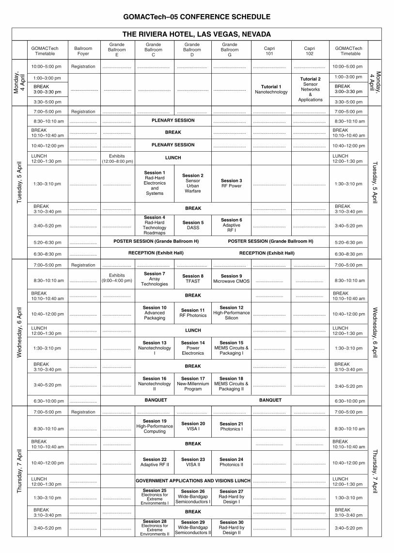
GOMACTechGrande Grande Grande Grande
GOMACTechBallroom Ballroom Ballroom Ballroom Ballroom Capri CapriTimetable Foyer E C D G 101 102 Timetable
10:00–5:00 pm Registration ....................... .......................... ........................ .......................... .......................... ......................... 10:00–5:00 pm
1:00–3:00 pm 1:00–3:00 pm
3:30–5:00 pm 3:30–5:00 pm
7:00–5:00 pm Registration ....................... .......................... ........................ .......................... .......................... .......................... 7:00–5:00 pm
8:30–10:10 am ...................... ....................... .......................... .......................... .......................... 8:30–10:10 am
BREAK BREAK10:10–10:40 am
...................... ...................... .......................... .......................... ..........................10:10–10:40 am
10:40–12:00 pm ...................... ....................... .......................... .......................... .......................... 10:40–12:00 pm
LUNCH ...................... Exhibits LUNCH12:00–1:30 pm (12:00–8:00 pm) 12:00–1:30 pm
1:30–3:10 pm ...................... ...................... .......................... .......................... 1:30–3:10 pm
BREAK BREAK 3:10–3:40 pm
...................... ....................... .......................... ..........................3:10–3:40 pm
3:40–5:20 pm ...................... ....................... .......................... .......................... 3:40–5:20 pm
5:20–6:30 pm ...................... 5:20–6:30 pm
6:30–8:30 pm ...................... 6:30–8:30 pm
7:00–5:00 pm Registration ....................... .......................... ........................ .......................... .......................... ......................... 7:00–5:00 pm
8:30–10:10 am ......................Exhibits
...................... ...................... 8:30–10:10 am(9:00–4:00 pm)
BREAK BREAK 10:10–10:40 am
...................... ...................... ...................... ......................10:10–10:40 am
10:40–12:00 pm ...................... ....................... .......................... .......................... 10:40–12:00 pm
LUNCH LUNCH12:00–1:30 pm
...................... ....................... .......................... ..........................12:00–1:30 pm
1:30–3:10 pm ...................... ...................... ......................... ........................ 1:30–3:10 pm
BREAK BREAK3:10–3:40 pm
...................... ....................... .......................... ..........................3:10–3:40 pm
3:40–5:20 pm ...................... ....................... .......................... ......................... 3:40–5:20 pm
6:30–10:00 pm ...................... 6:30–10:00 pm
7:00–5:00 pm Registration ....................... .......................... ........................ .......................... .......................... ......................... 7:00–5:00 pm
8:30–10:10 am ...................... ....................... .......................... .......................... 8:30–10:10 am
BREAK BREAK10:10–10:40 am
...................... ...................... ...................... ......................10:10–10:40 am
10:40–12:00 pm ...................... ....................... .......................... .......................... 10:40–12:00 pm
LUNCH LUNCH12:00–1:30 pm
...................... .......................... ..........................12:00–1:30 pm
1:30–3:10 pm ...................... ...................... .......................... .......................... 1:30–3:10 pm
BREAK BREAK3:10–3:40 pm
...................... ....................... .......................... ..........................3:10–3:40 pm
3:40–5:20 pm ...................... ....................... .......................... .......................... 3:40–5:20 pm
GOMACTech–05 CONFERENCE SCHEDULEM
onda
y,4
Apr
il M
onday, 4 A
prilT
uesd
ay, 5
Apr
il Tuesday, 5 A
prilW
edne
sday
, 6 A
pril W
ednesday, 6 April
Thu
rsda
y, 7
Apr
il Thursday, 7 A
pril
Tutorial 1Nanotechnology
Tutorial 2Sensor
Networks&
Applications
PLENARY SESSION
BREAK
BREAK
BREAK
BREAK
BREAK
BREAK
POSTER SESSION (Grande Ballroom H)
RECEPTION (Exhibit Hall) RECEPTION (Exhibit Hall)
BANQUET BANQUET
POSTER SESSION (Grande Ballroom H)
PLENARY SESSION
LUNCH
LUNCH
GOVERNMENT APPLICATIONS AND VISIONS LUNCH
Session 4Rad-Hard
TechnologyRoadmaps
Session 7Array
Technologies
Session 10AdvancedPackaging
Session 13Nanotechnology
I
Session 16Nanotechnology
II
Session 19High-Performance
Computing
Session 22Adaptive RF II
Session 25Electronics for
ExtremeEnvironments I
Session 28Electronics for
ExtremeEnvironments II
Session 8TFAST
Session 11RF Photonics
Session 14Power
Electronics
Session 17New-Millennium
Program
Session 20VISA I
Session 23VISA II
Session 26Wide-Bandgap
Semiconductors I
Session 29Wide-Bandgap
Semiconductors II
Session 9Microwave CMOS
Session 12High-Performance
Silicon
Session 15MEMS Circuits &
Packaging I
Session 18MEMS Circuits &
Packaging II
Session 21Photonics I
Session 24Photonics II
Session 27Rad-Hard by
Design I
Session 30Rad-Hard by
Design II
Session 6Adaptive
RF I
Session 2SensorUrban
Warfare
Session 5DASS
Session 3RF Power
Session 1Rad-Hard
Electronicsand
Systems
THE RIVIERA HOTEL, LAS VEGAS, NEVADA
...................... ...................... .......................... ......................... ..........................BREAK3:00–3:30 pm
BREAK3:00–3:30 pm
Session 15
MEMS CIRCUITS AND PACKAGING IWednesday, April 6 / 1:30 – 3:10 pm / Grande Ballroom G
Chair: Chuck GoldsmithMEMtronics Corp., Plano, TX
15.1: Reconfigurable MEMS-Enabled RF Circuits for (1:30) Spectrum Sensing
T. Mukherjee, G. K. Fedder, H. Akyol, U. ArslanCarnegie Mellon University, Pittsburgh, PA
Micromachining in RF foundry processes enhances inductor and capacitorquality factors, increases varactor tuning range, and supports creation ofelectromechanical mixer filters that downconvert from GHz to MHz withbuilt-in frequency selectivity. An on-chip parallel receiver architecture andcircuit blocks incorporating these devices for low-power operation will beintroduced.
15.2: Wideband and Multi-Octave MEMS-Reconfigurable RF Power Amplifiers (1:50)
S. LardizabalRaytheon RF Components, Andover, MA
B. Pillans, A. MalczewskiRaytheon Company APC, Dallas, TX
R. MolfinoRaytheon Integrated Defense Systems, Tewksbury, MA
Two adaptable microwave power amplifiers demonstrate frequency-agiletuning for the first time over wideband and multi-octave frequency ranges.Adaptable half-watt power amplifiers cover 8–12-GHz and 2–18-GHz frequency bands. Integrating and packaging MEM switching technology intoa GaAs PHEMT process is a key enabler.
15.3: Reliability Improvements in RF Capacitive MEMS Switches (2:10)
C. F. Kirby, R. M. Young, G. E. Dix, C. A. CapelleNorthrop Grumman Corp., Linthicum, MD
Two failure mechanisms in RF MEMS capacitive switches have been iden-tified: debris generation that causes the switch not to fully close and chargetrapping which prevents the switch from fully opening. Mitigation/eliminationof these mechanisms has led to improved switch reliabilities of 20 billioncycles (N50).
15.4: 20-GHz Distributed MEMS Phase Shifter Using Lateral Deflection MEMS Switches (2:30)
P. Chang-Chien, R. Stokes, D. Duan, K. TornquistNorthrop Grumman Space Technology, Redondo Beach, CA
Four-bit 20-GHz distributed MEMS transmission line (DMTL) phase shiftershave been demonstrated at NGST using lateral deflection RF MEMSswitches. These DMTLs have RMS phase errors of ~1 with power- handlingcapability of >1 W. Excellent switch uniformity and device yield makingthese lateral deflection MEMS switches suitable for large-array applications.
38
15.5: Packaging Technology for RF MEMS Switches (2:50)
D. Peroulis, L. P. B. KatehiPurdue University, West Lafayette, IN
Y. LuUniversity of Michigan, Ann Arbor, MI
RF MEMS switches impose very challenging performance and cost require-ments that are not met by todays packaging technology. Two alternatives toovercome this challenge will be presented. The first analyzes advancedpackaging schemes, while the second focuses on novel contact-less RFMEMS architectures with significantly more-forgiving packaging needs.
BREAK (3:10–3:40)
39
Session 16
NANOTECHNOLOGY IIWednesday, April 6 / 3:40 – 5:20 pm / Grande Ballroom C
Chair: Joe E. BrewerUniversity of Florida, Palm Coast, FL
Co-Chair: Meyya MeyyappanNASA–AMES Research Center, Moffett Field, CA
16.1: Post-CMOS: Biologically Inspired Computing (3:40)
D. HammerstromPortland State University, Portland, OR
Computational models inspired by biology, in particular, computational neuroscience, have much promise as an alternative to traditional comput-ing models. This is especially true for molecular scale implementation. Thestate of the art in neurobiological modeling and how such models mightmap to nano/molecular scale devices will be discussed.
16.2: Using Time and Redundancy for Nanocomputation (4:20)
J. Fortes, V. Ravinuthula, J. Harris, R. FigueiredoUniversity of Florida, Gainesville, FL
Based on previous work on time-based analog computation and new ideason how to quantize time, this paper proposes principles and building blocksfor digital time-based computation. Both nanoscaled CMOS and single-electronics device technologies were considered in strawman designs forthe needed blocks. Where nanosystems, including memories and FPGA-like systems, are implemented as addressable arrays of nanocells, hierar-chical redundancy schemes using spares and error codes were proposedfor fault-tolerance purposes.
16.3: Carbon-Nanotube Mid-Infrared Detectors Overlaid on Long-Infrared Focal-Plane Array (5:00)
N. XiMichigan State University, East Lansing, MI
H. Szu, J. BussONR, Arlington, VA
To reduce the noise-equivalent temperature in infrared sensors, carbonnanotubes (CNTs) were used as sensing materials because of its one-dimensional ballistic electronic-transport property. By simply modifying theshape of the CNT using a nano-robotic assembly system, the band gap ofa CNT can be tuned to 3–5-µm wavelengths of infrared radiation. The newarchitecture of an optical co-axial pixel plane was designed such that the 3–5-µm wavelengths detectors are overlaid above the 8–12-µm-wavelength focal-plane array (FPA). The co-axial pixel plane is fabricatedthrough the nano-robotic assembly system.
40
Session 17
NEW MILLENNIUM PROGRAMWednesday, April 6 / 3:40 – 5:20 pm / Grande Ballroom D
Chair: Raphael SomeJet Propulsion Laboratory, Pasadena, CA
17.1: DS2 Follow-on Experiment: Validation of DS2-Mars-Microprobe Impact-Surviving Technology (3:40)
B. Blaes, S. D’AgostinoJet Propulsion Laboratory, Pasadena, CA
An instrumented probe designed to impact the ground at ~180 m/sec hasbeen developed and field tested using an air gun. The probe design andimpact tests were successful at validating the impact-surviving design prin-ciples used in the building of NASA’s New Millennium Deep Space-2 (DS2)Mars microprobe.
17.2: The Space Technology 5 Microsatellite (4:00)Technology and Constellation Science Validation Mission
E. Webb, C. Carlisle, J. SlavinNASA-GSFC, Greenbelt, MD
The Space Technology 5 (ST-5) Project is part of NASA’s New MillenniumProgram that consists of a constellation of three 25-kg-class micro-satel-lites. The goals are to demonstrate the research-quality science capabilityof the ST-5 spacecraft, to operate the three spacecraft as a constellation,and to design and flight-validate three microsatellites with new technolo-gies. A 3-month flight-demonstration phase, beginning in March 2006, willvalidate the ability to perform science measurements, as well as the tech-nologies and constellation operations.
17.3: Flexible Architecture for Advanced System ThermalManagement (4:20)
D. Bugby, E. Kroliczek, J. Yun, J. GarzonSwales Aerospace, Beltsville, MD
A flexible two-phase-loop-based architecture for advanced system thermalmanagement will be described. The architecture, denoted as the multi-evaporator hybrid loop heat pipe (ME-HLHP), combines capillary pumpedloop (CPL) expandability and temperature controllability with loop-heat-pipe(LHP) operational robustness. Six specific implementations of ME-HLHPtechnology will be described.
17.4: Miniature-Loop Heat Pipe with Multiple Evaporators for Thermal Control of Small Spacecraft (4:40)
J. Ku, L. Ottenstein, D. DouglasNASA/GSFC, Greenbelt, MD
M. PaukenJet Propulsion Laboratory, Pasadena, CA
A miniature loop heat pipe having multiple evaporators and deployable radi-ators with variable emittance coatings on the radiators has been designed,fabricated, and tested. It combines the functions of variable conductanceheat pipes, thermal switches, thermal diodes, and the state-of-the-art LHPsinto a single integrated thermal system. Experimental results showed excel-lent performance and correlated well with theoretical predictions.
41
17.5: The Space Technology 7 Disturbance Reduction (5:00) System
W. FolknerJet Propulsion Laboratory, Pasadena, CA
The Space Technology 7 project will validate system-level technologies forfuture gravity and formation-flying missions. ST7 will control the spacecraftposition relative to freely floating test mass to within 10 nm using colloidalmicro-thrusters. The ST7 components will be flown as part of the EuropeanSpace Agency LISA in mid-2008.
17.6: New Millennium Program ST6: Autonomous (5:20)Technologies for Future NASA Spacecraft
A. B. Chmielewski, S. Chien, and R. SherwoodJet Propulsion Laboratory, Pasadena, CA
W. Wyman, T. Brady, S. Buckley, and C. TillierCharles Stark Draper Laboratory, Inc., Cambridge, MA
The purpose of NASA’s New Millennium Program (NMP) is to validateadvanced technologies in space and thus lower the risk for the first missionuser. The focus of the NMP is only on those technologies which need spaceenvironment for proper validation. The ST6 project has developed twoadvanced, experimental technologies for use on spacecraft of the future.These technologies are the Autonomous Sciencecraft Experiment and theInertial Stellar Compass. These technologies will improve the spacecraft’sability to make decisions on what information to gather and send back to theground and to determine its own attitude and adjust its pointing.
42
Session 18
MEMS CIRCUITS AND PACKAGING IIWednesday, April 6 / 3:40 – 4:40 pm / Grande Ballroom G
Chair: Chuck GoldsmithMEMtronics Corp., Plano, TX
18.1: High-Performance Packaging of RF MEMS Switches and Circuits (3:40)
C. D. Nordquist, C. W. Dyck, B. JokielSandia National Laboratories, Albuquerque, NM
T. LempOrion International, Albuquerque, NM
High-quality packaging is essential for achieving good performance, highyield, and low cost in MEMS-based circuits. This presentation will coverissues associated with several RF MEMS packaging approaches, includingusing commercial packages for parallel reliability testing, custom circuitpackages using LTCC, and wafer-level bonded packages.
18.2: Wafer-Level Microencapsulation (4:00)
D. Forehand, C. GoldsmithMEMtronics Corp., Plano, Texas
Microencapsulation is an innovative wafer-level packaging method for hermetically encapsulating RF MEMS switches. This packaging schemehas already demonstrated < 0.1-dB package insertion loss up through 50GHz. This presentation overviews the processes, performance, and testingmethods used for testing the hermeticity and insertion loss of individualencapsulated RF MEMS devices.
18.3: Wafer-Level RF MEMS Package (4:20)
E. BrownPhysical Domains, Inc., Los Angeles, CA
S. Cheung, M. Cohn, G. KimMicroAssembly Technologies, Inc., Richmond, CA
Packaging of RF MEMS poses multiple challenges, including loss, hermeticity, process temperature, and economics. In particular, substantialloses are associated with seal rings and thru wafer vias. Novel packagingapproaches are enabled by a transfer process. This transfer process iswafer-scale and uses only inorganic non-outgassing materials.
18.4: Hermetic Thin-Film Encapsulation for RF MEMS (4:00)Switches
J. L. Ebel, R. Cortez, K. D. Leedy, R. E. StrawserAFRL, Wright-Patterson AFB, OH
AFRL has developed, fabricated, and tested working RF MEMS switches inhermetic thin-film encapsulations. The hermeticity of the enclosures hasbeen verified using a vacuum RF testing process. The method of formingthe packaging, as well as the method of verifying hermeticity, will be presented.
43
18.5: Advanced RF MEMS Packaging (4:00)
J. Muldavin, C. Bozler, S. Rabe, C. KeastMIT Lincoln Laboratory, Lexington, MA
MIT Lincoln Laboratory has developed a wafer-scale low-loss broad-bandRF MEMS packaging technology. The fabrication includes CMOS-compati-ble front-end processing and thick Au back-end processing. Au thermo-compression bonding was used to mate a metal-coated capping wafer to adevice wafer, offering high-isolation and low-loss transmission lines withinthe cavity. Hermetic thru-wafer vias carry the rf signal in and out of the pack-age through the 25-µm-thick device wafer. A packaged 100-µm-long trans-mission line with 0.06 and 0.1 dB total insertion loss at 20 and 50 GHz,respectively, has been demonstrated. The packaged transmission line hasa 0.96-dB/cm attenuation at 40 GHz and less than ±1° phase error from dcto 50 GHz for a 10.8-mm-long line. The isolation of closely spaced lines willalso be presented. Hermeticity was evaluated with in-situ moisture sensorsafter submission to an autoclave environment for 10 hours.
44
THURSDAY, 7 APRIL
Session 19
HIGH-PERFORMANCE COMPUTINGThursday, April 7 / 8:30 –10:10 am / Grande Ballroom C
Chair: John GroshOffice of the Secretary of Defense, Rosslyn, VA
19.1: Multiprocessor Performance for Polymorphous (8:30)Computing Systems
D-I. Kang, S. P. Crago, J. Suh, C. Chen, M. C. FrenchUniversity of Southern California / Information Sciences Institute, Arlington, VA
Polymorphous computing architectures are being developed to provide highperformance across a wide range of DoD applications. A multiprocessorPCA prototype system will be described and measured application andcommunication performance results for a polymorphous architecture will beprovided.
19.2: Mapping Signal-Processing Kernels to Tiled (8:50)Architectures
H. Hoffmann, J. LebakMIT Lincoln Laboratory, Lexington, MA
A key feature of many new computer architectures is that they are com-posed of multiple tiles, each of which is a fully capable processor. Examplesof tiled architectures include many under development for the DARPA/IPTOPolymorphous Computer Architectures (PCA) program. A programmingparadigm called stream algorithms which has been shown to achieve highperformance on tiled architectures will be described.
19.3: Smart Memories: A Configurable Processor (9:10)Architecture for High-Productivity Parallel Programming
M. Horowitz, C. Kozyrakis, K. Olukotun, K. MaiStanford University, Stanford, CA
Smart memories are a novel architecture for next-generation general-purpose processors for highly parallel computations. Smart memories usea configurable memory system to support high-productivity high-perfor-mance parallel programming with streams or transactions for a wide rangeof regular and unstructured applications.
19.4: High-Performance Embedded Computing Systems for the Next Decade (9:30)
K. V. Palem, S. YalamanchiliGeorgia Institute of Technology, Atlanta, GA
The landscape of customization techniques for high-performance embed-ded computing (HPEC) systems will be described. As an illustrative exam-ple, experiences and performance results for compilation and optimizationof the MONARCH polymorphic computing architecture will be presented.The presentation concludes with a strategy for sustaining cost/performancegrowth for HPEC systems in the next decade.
45
19.5: Breaking the GOP/Watt Barrier with EDGE (9:50)Architectures
D. Burger, S. W. KecklerThe University of Texas at Austin, Austin, TX
The power efficiency (performance/Watt) of a new Explicit Data GraphExecution (EDGE) microprocessor architecture targetted at high-perfor-mance and embedded computing will be exaimed. The inherent structuralpower advantages of EDGE architectures over conventional high-perfor-mance architectures will be explored.
BREAK (10:10–10:40)
46
Session 20
VERTICALLY INTEGRATED SENSORARRAYS (VISA) I
Thursday, April 7 / 8:30 – 10:10 am / Grande Ballroom D
Chair: Ray BalcerakDARPA/MTO, Arlington, VA
20.1: Recent Developments in Vertically Integrated Sensor Arrays (8:30)
C. Fletcher, M. Skele, R.W. Graham, M. TangRaytheon Vision Systems, Goleta, CA
3-D vertically interconnected sensor arrays have been developed. Thesefocal-plane-array assemblies have been processed from whole wafersdown to individual stacked die with dense via interconnects. RaytheonVision Systems has been working with the State University of New York onthe Vertically Integrated Sensor Array program, a technology-developmentprogram funded by DARPA. This program was tasked with developing 3-Dstacked ROICs for imaging sensors, and also the development of high-performance circuitry which will reside in the 3-D ROIC stack.
20.2: Vertically Interconnected Sensor Array (VISA) (8:50)Technology for High-Operating-Temperature HgCdTe Focal Plane Arrays
J. Robinson, L. Wood, T. Murphy, P. Coffman DRS Infrared Technologies, Plano, TX
HgCdTe focal-plane arrays offer the ultimate in IR sensitivity and havefound widespread application in the highest-performance IR mili-tary systems. VISA technology is being development to achieve even higher-performance levels by providing increased signal processing at thepixel level for applications such as laser-jamming avoidance, active imag-ing, and multicolor FPAs.
20.3: High-Density 3-D Interconnect Technology for (9:10)Massively Parallel Signal Processing in IR FPAs
D. Temple, D. Malta, B. R. Stoner, C. A. Bower MCNC-RDI, Research Triangle Park, NC
3-D interconnect technology has the potential to dramatically enhance signal-processing capabilities of high-resolution staring focal-plane-array(FPA) devices. The technology provides for heterogeneous integration ofthe 2-D detector arrays with multiple layers of silicon ICs by means of insulated and metallized vias etched through the body of the IC chips.
20.4: Process Development of Z-Axis Interconnects Using Fine-Pitch Through Silicon Vias (9:30)
L. Schaper, S. Spiesshoefer, S. Burkett, G. VangaraUniversity of Arkansas, Fayetteville, AK
The University of Arkansas has been working on an alternative through-silicon via (TSV) process technology for the VISA program. The goal hasbeen to create thin, freestanding silicon slices for subsequent parallelassembly. The UA focus has been on producing TSVs using copper plating.Implementation of the UA process for TSVs has included five main fabrica-tion areas: formation of the vias, deposition of the insulation and seed lay-ers, copper plating, wafer thinning, and system integration. The project goalis to create high-aspect-ratio vias 4–6 µm in diameter on 20-µm pitch inwafers that are subsequently thinned to a thickness of about 20 µm.
47
20.5: VISA Architecture for High-Dynamic-Range Two-Color IR Focal Planes (9:50)
D. Cooper, J. Denatale, S. Lauxtermann, P. O. PetterssonRockwell Scientific Co., Camarillo, CA
A 3-D interconnect approach was developed based on fine-pitch high-aspect-ratio through wafer vias in relatively thick (250 µm) silicon wafers,enabling vertically interconnected sensor array (VISA) focal-plane arrays(IR FPAs). The mechanical durability of these thicker parts permits die-levelassembly of known good die, using indium interconnect technology,increasing the ultimate yield of devices. The indium interconnect approachhas been used to fabricate hybrid infrared focal planes for many years andis a mature technology. The extension to the VISA architecture requires thatmultiple layers be connected by depositing indium interconnects on bothsides of the intermediate layers before mating.
BREAK (10:10–10:40)
48
Session 21
PHOTONICS IThursday, April 7 / 8:30 – 10:10 am / Grande Ballroom G
Chair: Ravindra AthaleDARPA/MTO, Arlington, VA
21.1: Optical Detection of Chemical-Warfare Agents and Toxic Industrial Chemicals (8:30)
C. Kumar, N. PatelUCLA and Pranalytica, Santa Monica, CA
M. Webber, M. Pushkarsky, T. MacdonaldPranalytica, Santa Monica, CA
The modeling of laser photoacoustic spectroscopy (L-PAS), which permitsthe attainment of a generalized performance evaluation methodology forCWA, and TIC sensors has been carried out. Both a detailed simulation aswell as preliminary experimental results that show that tunable-laser-basedL-PAS will be able to provide a sub-ppb sensor for CWAs and PFP less thanone part in a million with a measurment time of less than 30 sec will bedescribed. The analysis is applicable to any optical sensor and provides ageneralized scheme for performance optimization.
21.2: Volume Bragg Gratings for Sensing and Processing Applications (8:50)
L. B. GlebovUniversity of Central Florida, Orlando, FL
New robust material for holographic optical elements has been created,which is a photo-thermo-refractive (PTR) glass. Transmitting and reflectingBragg gratings with a diffraction efficiency up to 98% and an aperture up to35 mm will be demonstrated. Application of these new elements for sensingand laser-beam control will discussed.
21.3: Infrared Photonics for Sensing Applications Using Chalcogenide Glasses
N. C. Anheier, J. F. Schultz Pacific Northwest National Laboratory, Richland, WA
Recent developments at Pacific Northwest National Laboratory in the areaof photonics for infrared-sensing applications using chalcogenide glasseswill be reported. Both direct-laser writing and holographic exposure tech-niques show promise for developing useful infrared photonic devices.
21.4: Coded Sampling for Increased Resolution and Higher Sensitivity Optical Spectroscopy and Imaging (9:10)
D. J. Brady, N. Pitsianis, M. Gehm, S. McCainDuke University, Durham, NC
Multiplex codes and computational sensing enable the size (thickness andvolume) of optical imagers and spectrometers to be reduced by severalorders of magnitude while increasing sensitivity and resolution.
49
WITHDRAWN
21.5: PANOPTES: A Thin Agile Multi-Resolution Imaging Sensor (9:30)
M. P. Christensen, S. Douglas, D. RajanSouthern Methodist University, Dallas, TX
M. W. HaneyUniverisity of Delaware, Newark, DE
S. WoodSanta Clara University, Santa Clara, CA
A thin agile multi-resolution imaging sensor called PANOPTES will be intro-duced. It is a tiled architecture consisting of micromirror arrays, detectorarrays, and micro-optical elements. Individual tiles are directed to areas ofthe scene with increased information content, thereby matching the sens-ing capacity of the architecture to the scenes information content.
BREAK (10:10–10:40)
50
Session 22
ADAPTIVE RF IIThursday, April 7 / 10:40 am – 12:00 pm / Grande Ballroom C
Chair: Eric D. AdlerArmy Research Laboratory, Adelphi, MD
Co-Chair: William D. PalmerArmy Research Laboratory, Adelphi, MD
22.1: Integrated Spectral BIST Technique for IRFFE Systems (10:40)
J. M. EmmertUniversity of North Carolina at Charlotte, Charlotte, NC
J. A. CheathamWright State University, Dayton, OH
The reconfigurable built-in self-test (BIST) technique for integrated mixed-signal (digital, analog, and RF) systems will be described. Unlike digital sys-tems, BIST for analog and RF systems is difficult to develop due to the inex-act nature of analog signals and the complexity of the test circuitry. By tak-ing advantage of low-area-overhead techniques, a spectral BIST approachallows for the incorporattion of test-signal generation and the analysis of analog and RF systems on the same integrated die as the circuits themselves.
22.2: Adaptive Biasing of High-Efficiency X-band PAs for Power Control and Linearity (11:00)
Z. Popovic, D. Maksimovic, N. Wang, P. Bell, V. Youzefzadeh, S. PajicUniversity of Colorado, Boulder, CO
Multifunctional intelligent RF front ends require a variety of bias levels thatcan be dynamically adjusted to optimize performance. The adaptive effi-ciency optimization of a transmitter power amplifier (PA) will be addressed.X-band high-efficiency (> 60%) PAs are designed with efficient fast andslow feedback, which controls the bias to maintain efficiency while varyingoutput power and/or improving linearity.
22.3: Toward a Multifunctional LFM-Waveform (11:20)Communications/Radar System: Single-Crystal AlN-on-SiC SAW Filters for X Band
G. N. Saddik, E. R. BrownUniversity of California, Santa Barbara, CA
A new breed of SAW filter based on single-crystal AlN, a material that hasimproved significantly in recent years with advances in nitride-compoundepitaxy, will be addressed. Simulations for the SAW bandpass filter at X-band will be presented. Near-ideal insertion loss, bandwidth, and out-of-band rejection was observed. Presently, the device is in fabrication andexperimental results will be reported.
51
22.4: Insulated-Gate PHEMT Switching Devices Fabricated with a Low-Temperature-Grown (LTG) GaAs Gate Insulator (11:40)
R. Actis, K. Nichols, D. Xu, X. YangBAE SYSTEMS, Nashua, NH
A novel insulated-gate PHEMT for use in low-loss Ka-band switch applica-tions will be described. Using a highly insulating low-temperature-grown(LTG) GaAs material for the gate insulator, a submicrometer-gate-lengthPHEMT switch device has exhibited significantly improved switching char-acteristics over conventional PHEMTs, including a 1-Ω-mm on-state resis-tance (at several volts forward-bias) and a 20-V device breakdown voltage.
GOV’T APPLICATIONS & VISIONS LUNCH (12:00–1:30)
52
Session 23
VERTICALLY INTEGRATED SENSORARRAYS (VISA II)
Thursday, April 7 / 10:40 am – 12:00 pm / Grande Ballroom D
Chair: Ray BalcerakDARPA/MTO, Arlington, VA
23.1: Advances in Lincoln Laboratory’s 3-D Circuit (10:40)Technology
J. Burns, B. Aull, C. K. Chen, C. KeastMIT Lincoln Laboratory, Lexington, MA
Functional 3-D ring oscillators and 1048 × 1048 visible imagers have beenfabricated with Lincoln Laboratory’s 3-D circuit-integration technology. Thebuilding blocks of the technology are fully depleted SOI technology circuitfabrication, precision wafer-wafer alignment, low-temperature oxide bond-ing, and the construction of dense 3-D electrical interconnections.
23.2: Electrical Model to Hardware Correlation of Through Wafer Vias for Wafer-Stacking Technology (11:00)
M. LorsungMayo Clinic, Rochester, MN
One of the goals of DARPA’s Vertically Interconnected Sensor Array (VISA) program is to provide an enabling technology for the stacking of siliconread-out integrated circuits (ROICs) where vertical through wafer vias pro-vide connection from one chip to another in a chip sandwich stack. By pro-viding a silicon stacking technology, additional functionality could be real-ized beneath each of the optical electrical transducers in a N x M detectorarray.
23.3: VISA Architectures for HDR and Low Light Detection
S. Kavusi, A. El GamalStanford University, Stanford, CA
Focal-plane-array architectures that take advantage of vertical integrationto achieve unprecedented levels of performance will be described. Twoschemes will be discussed: (1) folded-multiple capture with backgroundsubtraction that is capable of achieving over 20 bits of DR, at high fidelityand low power, and (2) correlated multiple sampling for achieving ultra-lowlight detection.
23.4: Focal-Plane Architecture with On-Chip ADC and Compression for High-Resolution High-Speed Digital Video Capture (11:20)
L. McIlrath, C. Cheung, J. DowellR3 Logic, Inc., Cambridge, MA
A new CMOS readout architecture that provides near lossless in-streamcompression of 10-bit video data at rates up to 1000 frames per second onlarge focal-plane arrays will be presented. The correctness of the circuitdesign in performing all logic operations at data rates of interest has beenfully tested and verified in fabricated prototype arrays. The architecture canbe combined with different sensing materials through 3-D integration to permit imaging in different spectral regions.
GOV’T APPLICATIONS & VISIONS LUNCH (12:00–1:30)
53
WITHDRAWN
Session 24
PHOTONICS IIThursday, April 7 / 10:40 am – 12:00 pm / Grande Ballroom G
Chair: Ravindra AthaleDARPA/MTO, Arlington, VA
24.1: The Future of Optical Processing (10:40)
T. M. Turpin, C. PriceEssex Corp., Melbourne, FL
The future of optical processing will be projected based on the history of thetechnology and the common features of failed efforts and successful oper-ational processors.
24.2: Ultra-Wideband Analog Optical Signal Processing of Complex Waveforms for Range Doppler Radar (11:00)Measurements
R. Reibel, K. D. MerkelScientific Materials Corp., Bozeman, MT
Z. Cole, D. E. BensonMontana State University, Bozeman, MT
Real-time ultra-wideband (>2 GHz) analog signal processing is experimen-tally demonstrated utilizing electro-optical devices and spectrally selectiveoptical materials. A range resolution of 20 cm and a Doppler resolution of125 Hz has been demonstrated. Complex, large-time bandwidth productanalog RF waveforms, including band-limited white noise, can beprocessed on S-, L-, and X-band carriers without down-conversion.
24.3: Broadband Blind RF Signal Separation with (11:20)Optoelectronic ICA
P. Smith, M. Baylor, K. Erickson, Z. PopovicUniversity of Colorado, Boulder, CO
An optoelectronic solution to the communications problem of blind-sourceseparation for broadband RF signal sources will be presented. The inde-pendent component analysis (ICA) system is capable of dynamic 45–60-dBsignal separation for a two-channel case. The signals are completelyunknown, can have overlapping spectra, and can originate within abeamwidth of a small-aperture antenna array.
24.4: Light-Emitting Transistor Array for Optical (11:40) Interconnect Application
M. Feng, N. Holonyak, Jr., R. Chan, G. WalterUniversity of Illinois at Urbana-Champaign, Urbana, IL
The future applications and current progress of InGaP/GaAs heterojunctionbipolar light-emitting transistor (HBLET) development for the electronicsand optical communications application will be reported. DC and RF per-formance of an 80-Å QW embedded HBLET with an emitter mesa dimen-sion of 6 x 7 m2 will be reported. A fabricated device has a beta of 5, ft of 14.5 GHz at an emission wavelength of 970 nm. The monolithically inte-grated 2 x 3 array operation of circular HBLETs will also be reported.
GOV’T APPLICATIONS & VISIONS LUNCH (12:00–1:30)
54
Session 25
ELECTRONICS FOR EXTREME ENVIRONMENTS I
Thursday, April 7 / 1:30 – 3:10 pm / Grande Ballroom C
Chair: Elizabeth KolawaJet Propulsion Laboratory, Pasadena, CA
25.1: Considerations for the Operation of Electronics inExtreme Environments (1:30)
Elizabeth KolawaJet Propulsion Laboratory, Pasadena, CA
During the next 20 years, NASA will be challenged to develop the neces-sary technologies to support missions to extremely diverse environments.In one extreme, Venus Surface Exploration missions require systems thatare able to survive and operate in high-temperature (460°C) and high-pres-sure (90 bar) environments. Survivability in extremely high temperatures(380°C) and high pressures (1000 bar) is also required for deep atmos-pheric multiprobes to Giant planets. On the other extreme, Comet NucleusSample Return, Titan, Europa, and Moon exploration will require systemsable to survive in extremely cold environments in the -140 to -230°C temperature range. In addition, the Europa mission presents a challenge of surviving in extremely cold temperatures (-160°C) and high-radiation (5 Mrad) environments. Missions to Mars present the challenge of survivingextreme temperature cycling (-120 to +20°C).
25.2: Using SiGe HBT Technology for Emerging ExtremeEnvironment Electronics Applications (1:50)
J. D. CresslerGeorgia Tech, Atlanta, GA
It is argued that SiGe HBTs offers potential to simultaneously satisfyextreme environment electronics applications involving radiation tolerance,cryogenic temperatures, and/or high temperatures, potentially with little orno process modification, providing compelling cost advantages at both theIC and system level.
25.3: Emerging Heterogeneous Integration Technologies forExtreme Environment (2:10)
H. Sharifi, S. MohammadiPurdue University, West Lafayette, IN
M. M. MojarradiJet Propulsion Laboratory, Pasadena, CA
A heterogeneous integration technology suitable for electronic packagingfor harsh environments has been developed. The idea is to embed a Si(MEMS, III/V) chip inside a Si carrier substrate (glass, quartz, LCP) withseamless transitions between the chip and substrate. Interconnect lineswith widths of 25 µm was easily fabricated.
55
25.4: Extreme-Environment Electronics by Design (2:30)
T. J. Thornton, H. BarnabyArizona State University, Tempe, AZ
B. J. BlalockUniversity of Tennessee, Knoxville, TN
M. M. MojarradiJet Propulsion Laboratory, Pasadena, CA
Design techniques that can be used with conventional integrated-circuitprocesses for the development of low-cost electronic circuits and systemsthat operate reliably in extreme environmental conditions, including ultra-low, ultra-high, and ultra-wide temperature ranges combined with high radi-ation levels, will be presented.
25.5: Design, Modeling, and Characterization of Power MOSFET in 4H-SiC for Extreme-Environment (2:50)Applications
M. Hasanuzzaman, S. K. Islam, L. M. TolbertUniversity of Tennessee, Knoxville, TN
The theoretical limitations of silicon-based switching devices for high-powerand high-temperature applications can be overcome by the emerging mate-rial silicon carbide (SiC) and can be used in extreme environments, espe-cially in hybrid electric-vehicle applications. An analytical model of a verticalDIMOS transistor structure, a frequently used switching device in powerelectronics system design, will be presented.
BREAK (3:10–3:40)
56
Session 26
WIDE-BANDGAP SEMICONDUCTORS IThursday, April 7 / 1:30 – 3:10 pm / Grande Ballroom D
Chair: Dave ViaAFRL, Wright-Patterson AFB, OH
26.1: Progress in Advanced PVT Growth of SiC Substrates for RF and High-Power Electronic Applications (1:30)
T. A. Anderson, D. L. Barrett, J. L. Chen, E. EmorhokporII-VI, Inc., Pine Brook, NJ
An advanced PVT (APVT) process for the growth of SiC single crystals hasbeen developed. The proprietary process utilizes a high-purity SiC sourceand employs special measures aimed at the reduction of contamination by nitrogen, boron, and other background impurities. The APVT-grownmaterial demonstrates concentrations of B and N reduced to about 2 × 1015 cm3 and metals (Fe, Cr, Ni) to 1012–1014 cm-3. The X-ray scan-ning yields wafer maps of the Bragg reflection broadening (FWHM) as wellas angular misorientation between the sub-grains. Representative sampleswere evaluated using EPR and photoluminescence, which give informationon the nature of native point defects and their complexes.
26.2: Production-Scale MOCVD Growth of High-Power High-Frequency AlGaN/GaN HEMTs (1:50)
S. Guo, B. Albert, M. Pophristic, I. EliashevichEMCORE Corp., Somerset, NJ
AlGaN/GaN HEMTs are of interest for high-power and high-frequencydevice applications due to their superior material properties. MOCVDgrowth shows great promise for volume production growth of high-perfor-mance AlGaN/GaN HEMTs on large-area substrates. For commercial appli-cations, wafer size is a very important factor in final device cost, especiallyfor power electronics, where individual devices can be quite large, up toseveral square millimeters. In this work, the production MOCVD growth ofAlGaN/GaN HEMTs on 2- and 3-in. SiC as well as on 4-in. sapphire will beaddressed. Results of epitaxial material characterization and RF devicetesting at frequencies from 2 to 40 GHz will be presented.
26.3: Progress in SiC MMIC Production Readiness and High-Efficiency GaN Amplifiers (2:10)
J. MilliganCree, Inc., Durham, NC
SiC MMIC and GaN device technologies have progressed rapidly over thelast 3 years. High-power SiC MMICs are now being produced in quantity ina commercial MMIC foundry with high yield and reliability. The technologyis now a serious consideration for many upcoming military systems as ahigher-voltage alternative to high-voltage GaAs. Technical performance andyield statistics for a run of over 2000 high-power SiC MMICs will be pre-sented. Additionally, SiC device reliability data will be presented, showing aminimum reliability of 106 MTTF hours at a TJ of 175°C.
57
26.4: DARPA WBGS GaN Materials Development at (2:30)Raytheon
J. Smolko, S. Brierley, W. Hoke, R. HallockRaytheon, Tewksbury, MA
State-of-the-art GaN technology, based on HEMT structures grown byMBE, has been developed. The current status of this development, both forGaN HEMT epitaxy and device performance, will be discussed. Resultsfrom a production GaN reactor showing good uniformity and reproducibilityof AlGaN/GaN HEMT epi structures on SiC substrates up to 100 mm indiameter will be presented. State-of-the-art device results on 1.25-mm FETsdemonstrating 10-GHz power-added efficiencies in excess of 60% at 30-Vdrain bias, with good performance maintained up to 50-V drain bias, will bepresented.
26.5: AlGaN/GaN on SiC and on Si for RF Power (2:50)Applications
P. Saunier, C. Lee, D.C. Dumka, H.Q. TserngTriQuint Semiconductor, Richardson, TX
Excellent results have been achieved with GaN-on-SiC devices using field-plate gates; 8.6 W/mm with a 59% PAE at 10 GHz has been demonstrated.Recently, very promising performance using GaN-on-Si devices with 7 W/m has been demonstrated.
BREAK (3:10–3:40)
58
Session 27
RAD-HARD BY DESIGN IThursday, April 7 / 1:30 – 3:10 pm / Grande Ballroom G
Chair: Daniel J RadackDARPA/MTO, Arlington, VA
27.1: Robust Optimization for Rad-Hard Analog/RF (1:30)Circuits
X. Li, J. Wang, K. Y. Tong, L. T. PileggiCarnegie Mellon University, Pittsburgh, PA
A novel robust-analog-design tool (ROAD) to minimize the impact of analogsingle-event transients due to ion strikes and circuit behavior uncertaintydue to process variations will be presented. A low-noise-amplifier examplewas used to demonstrate the efficacy of the proposed methodology.
27.2: Rad-Hard by Design Approaches Applied to Structured ASIC Applications (1:50)
D. Mavis, P. Eaton, M. Sibley, M. MostromATK Mission Research, Albuquerque, NM
Special layout and circuit-design techniques were used to achieve radiationhardness to both total ionizing dose and single-event effects in high-density deep submicron structured ASICs. The approach promises to pro-vide inexpensive high-performance rad-hard parts using commercial fabri-cation processes.
27.3: Implementation of High-Speed Circuits for Analysis of Single-Event Effects (2:10)
B. Randall, S. Currie, K. Fritz, J. CokerMayo Clinic, Rochester, MN
Under the DARPA/MTO Radiation Hardened by Design Program, MayoClinic Rochester is investigating SiGe BiCMOS technology for its toleranceto single-event effects. This analysis was accomplished through the imple-mentation of test circuits as well as special test fixtures that enable the inte-grated circuits to be tested in a radiation chamber while operating at highspeed. Results of this work will be presented.
27.4: One-Mask-Structured ASIC Technology for (2:30)Cost-Effective Rad-Hard ICs
B. Cox, P. DewellViASIC, Durham, NC
D. Mavis, P. EatonATK Mission Research, Albuquerque, NM
J. KimerlingTriad Semiconductor, Winston-Salem, NC
Recent advances in HBD techniques for deep sub-micron designs enablefabrication of rad-hard ICs through commercial foundries. A unique one-mask-structured ASIC approach, designed with these techniques, enablesaffordable rad-hard ICs in low volume that contain high-quality digital circuits and future support for integrated mixed-signal capability.
59
27.5: Rad-Hard Library Synthesis (2:50)
W. P. Snapp, Z. A. Johnson, M. P. Baze, J. W. ClementBoeing Airplane Co., Seattle, WA
Rad-hard mixed-signal libraries both for hardened and non-hardened com-mercial fabrication processes, such as provided by the dedicated rad-hardfoundries and the DoD Trusted Foundry, are being developed. Innovativefoundry flexible library synthesis and hardening-by-design techniques wereused and the libraries were integrated into a silicon compiler EDA designflow. The methodology and results of this program will be reported.
BREAK (3:10–3:40)
60
Session 28
ELECTRONICS FOR EXTREME ENVIRONMENTS II
Thursday, April 7 / 3:40 – 5:20 pm / Grande Ballroom C
Chair: Elizabeth KolawaJet Propulsion Laboratory, Pasadena, CA
28.1: Packaging Technology for Extreme-Environment (3:40)Electronics
R. W. Johnson, J. WilliamsAuburn University, Auburn, AL
The challenges of packaging SiC power devices for high temperaturesinclude high operating temperature, wide thermal cycle range, high cur-rents, and high voltages. Ongoing research to develop suitable materialsand processes for packaging SiC power devices, including high-tempera-ture ohmic and Schottky contacts, die attach wire bonding, and passivation,will be discussed.
28.2: The Need for a High-Temperature Electronics (4:00)Standard
R. NormannSandia National Laboratories, Albuquerque, NM
Extreme environments require a complete solution before electronic controland data acquisition systems can be valued by the end customer. For thecase of high temperatures (150ºC and above), the elimination of all heat-shielding or active-cooling benefits the end consumer, justifying the addedexpense of extreme electronic components. Following two DOE-sponsoredworkshops, both small and large component manufacturers have asked fora “general” component standard to help unify the extreme environmentalmarkets (i.e., aircraft engines, automotive, deep drilling).
28.3: One-Year Well Test at 192.5ºC (4:20)
R. Normann, J. Henfling, D. ChaviraSandia National Laboratories, Albuquerque, NM
In October 2003, a complete high-temperature logging tool was deployedwithin a geothermal well. The well was 192.5ºC, located on the Coso Navytest range. The tool contained a complete set of Honeywell HT SOI elec-tronics, polyimide printed wiring board, wires, solders, pressure seals, inter-connects along with Quartzdyne quartz pressure and temperature sensors.The results after the first year will be reported and suggestions for improve-ments will be described.
28.4: Model-Based Design Tools for Extreme (4:40)Environments
A. Mantooth, M. Vlach, J. ShieldsLynguent, Portland, OR
Model-based design (MBD) tools to predict the performance and useful lifeof electrical components and systems subjected to extreme environmentalconditions will be described. These tools will consist of novel modeling toolsand advanced system and data analysis capability.
61
28.5: Operation of a Boost Converter in an Extremely (5:00)Low-Temperature Environment
R. M. Nelms, D. He, C. CutshawAuburn University, Auburn, AL
Power will be required for the electronic systems operating in the extremecold environments for some future NASA missions. The focus of this effortis the investigation into the operation of a power converter at low tempera-tures using COTS components.
62
Session 29
WIDE-BANDGAP SEMICONDUCTORS IIThursday, April 7 / 3:40 – 5:20 pm / Grande Ballroom D
Chair: Chris BozadaAFRL, Wright-Patterson AFB, OH
29.1: Wideband and Low-Power AlGaN/GaN HEMT MMIC Robust Low-Noise Amplifier (3:40)
A. Kurdoghlian, H. Moyer, M. Micovic, D. ChowHRL Laboratories, Malibu, CA
Superior RF power performance from GaN HFET technology has beendemonstrated by several groups over GaAs pHEMT technology. GaN HFETtechnology also has strong potential for harsh-environment receiver appli-cations due to the robust nature of GaN HFETs. Despite being wide-bandgap devices, GaN HFETs have demonstrated excellent noise perfor-mance at remarkably low bias power levels of less than 15 mW, whichmakes them ideal candidates for front-end receivers in phase-array antennas.
29.2: GaN for Ka-Band Solid-State Power Amplifiers (4:00)
M. Wojtowicz, R. Coffie, P-P. Huang, I. SmorchkovaNorthrop Grumman Space Technology, Redondo Beach, CA
GaN technology is emerging as the superior microwave and millimeter-wave technology for solid-state power amplification for military, space, andcommercial applications. The high breakdown voltage and good thermalconductivity of the AlGaN/GaN material system on SiC enables new levelsof solid-state power and robust low-noise amplifier performance.
29.3: DARPA Wideband-Gap Semiconductor Technology Initiative (WBGSTI) Tri-Service Observations (4:20)
G. D. ViaAFRL, Wright-Patterson AFB, OH
S. C. Binari, E. GlaserNaval Research Laboratory, Washington, DC
D. JudyArmy Research Laboratory, Adelphi, MD
Phase I of DARPAs Wide Bandgap Semiconductor Technology Initiative(WBGSTI) will be completed by the end of the 2004. Deliverables from thisprogram, including substrates (SiC, AlN, and GaN), AlGaN/GaN HEMT epi-taxy, and processed device wafers, are being evaluated by the Tri-Serviceteam. A summary of Tri-Service observations will be presented. In additionto the baseline measurements, several critical experiments have been performed in response to technical challenges that have arisen during theprogram. Select experiments will be described and the findings discussed.
63
29.4: Highly Survivable Wideband GaN HEMT Low-Noise Amplifier (4:40)
J. M. Yang, S. Cha, Y.H Chung, M. WojtowwiczNorthrop Grumman Space Technology, Redondo Beach, CA
GaN has emerged as the technology of choice for next-generation high-power electronics. However, its ability to handle high input power alsomakes it an ideal candidate for a highly survivable receiver component. Thisfeature directly translates MMIC compaction and cost saving because nofront-end protection circuitry is required. A wideband GaN HEMT low-noiseamplifier using novel dual-gate topology is being designed, fabricated, andtested in fixture to demonstrate a suvivability of greater than 38 dBm.
29.5: Advanced GaN HFETs for Millimeter-Wave (5:00)Applications
M. Micovic, M. Delaney, J. Moon, A. KurdoghlianHRL Laboratories, Malibu, CA
The development of advanced GaN HFET technology for millimeter-waveapplications will be reported. The GaN MMIC process, which has demon-strated excellent uniformity on four sapphire wafers and three SiC wafers,consistently yields low contact resistance, good buffer isolation, low gateleakage current, and good pinch-off characteristics.
64
Session 30
RAD-HARD BY DESIGN IIThursday, April 7 / 3:40 – 4:40 pm / Grande Ballroom G
Chair: Daniel J RadackDARPA/MTO, Arlington, VA
30.1: Advanced Electronics Technologies: Challenges forRadiation Effects Testing, Modeling, and (3:40)Mitigation
K. A. LaBelNASA/GSFC, Greenbelt, MD
L. M. CohnDTRA, Ft. Belvoir, VA
As plans for space utilization of sub-100-nm digital CMOS technologies andultra-high-speed mixed-signal technologies gather interest, the issuesrelated to how radiation effects the performance of these technologies pro-vide a significant challenge. These challenges will be discussed, withemphasis on single-event effects and total ionizing dose.
30.2: IBM Silicon Technologies in the Trusted FoundryProgram (4:00)
G. CarlsonIBM RTP, NC
IBM will discuss the status of their participation in the Trusted Foundry pro-gram. This will highlight the advanced processes available under the program, and a description of how to engage in it
30.3: The Fabrication of Rad-Hard by Design Circuitsthrough the Trusted Foundry (4:20)
D. Both, G. EtzoldNSA/TAPO, Ft. George G. Meade, MD
The Trusted Foundry provides access to leading-edge semiconductor fab-rication services and assures the customers against loss of confidentialityor protection against exploitation of the supply chain. The progress employ-ing multi-project wafers on the first runs will be descibed, the process forobtaining services will be reviewed, and future directions will be discussed.
65
GOMACTech-05 STEERING COMMITTEE
Conference Chair:Ingham MackOffice of Naval Research, Washington, DC
Technical Program Chair:Sammy KayaliJet Propulsion Laboratory, Pasadena, CA
Local Arrangements Chair:William D. PalmerU.S. Army Reseaerch Office, Research Triangle Park, NC
Finance Chair:Gerald BorsukNaval Research Laboratory, Washington, DC
Secretary:Arthur CampbellNaval Research Laboratory, Washington, DC
Conference Coordinator:Ralph NadellPalisades Convention Management, New York, NY
Awards Chair:Stephen KnightNIST, Gaithersburg, MD
Steering Committee Representatives:Eric AdlerArmy Research Laboratory, Adelphi, MD
Charles D. CaposellNaval Air Systems Command, Patuxent River, MD
John FrancoDefense Threat Reduction Agency, Alexandria, VA
Phillip HowertonNational Reconnaissance Office, Chantilly, VA
Chris LesniakAFRL/Wright-Patterson AFB, OH
John PellegrinoArmy Research Laboratory, Adelphi, MD
Harold SchoneJet Propulsion Laboratory, Pasadena, CA
John ZolperDARPA/MTO, Arlington, VA
66
GOMACTech-05 TECHNICAL PROGRAM COMMITTEE
Technical Program Chair:Sammy Kayali
Jet Propulsion Laboratory, Pasadena, CA
Technical Program Committee:
Eric D. AdlerArmy Research Laboratory, Adelphi, MD
Gerald BorsukNaval Research Laboratory, Washington, DC
Joe BrewerIEEE, Palm Coast, FL
Arthur CampbellNaval Research Laboratory, Washington, DC
Charles CaposellNaval Air Systems Command, Patuxent River, MD
Brian CohenIDA, Alexandria, VA
Phillip HowertonNational Reconnaissance Office, Chantilly, VA
Stephen KnightNIST, Gaithersburg, MD
Christopher LesniakAFRL, Wright-Patterson AFB, OH
Loren LinholmConsultant, Ijamsville, MD
Ingham MackOffice of Naval Research, Arlington, VA
Edgar J. MartinezPurdue University, West Lafayette, IN
William D. PalmerArmy Research Office, Research Triangle Park, NC
John PellegrinoArmy Research Laboratory, Adelphi, MD
Dan RadackDARPA/Arlington, VA
Harold SchoneAir Force Research Laboratory, Kirtland AFB, NM
67

68