Embed Size (px)
Citation preview
8/12/2019 Graded Optical Filters
http://slidepdf.com/reader/full/graded-optical-filters 1/164
Graded Optical Filters in Porous Siliconfor use in MOEMS Applications
by
Sean Erik Foss
Submitted
in partial fulfilment of the requirementsfor the degree of
Doctor Scientarium
Department of PhysicsFaculty of Mathematics and Natural Sciences
University of Oslo
Oslo, Norway September, 2005

8/12/2019 Graded Optical Filters
http://slidepdf.com/reader/full/graded-optical-filters 2/164

8/12/2019 Graded Optical Filters
http://slidepdf.com/reader/full/graded-optical-filters 3/164
Abstract
Combining optics, electronics and mechanics on one miniature platform isan emerging reality in micro device technology. An important goal of thisis the simplification and enhancement of actions in every-day life, e.g. lab-
on-a-chip for full characterization of blood samples with integrated loading,transportation, manipulation and analysis on one chip. Many elements arerequired for this to work, among them the control and manipulation of light.
This thesis presents a study of the use of porous silicon within this scope.Optical filters changing the spectral characteristics of light are fabricatedin an electrochemical etching process of silicon in solutions containing hy-drofluoric acid. The aim of this investigation is to fabricate high quality op-tical transmission and reflection filters in the near-infrared making use of thespecial properties of porous silicon which are hard to achieve in other opti-cal materials, and at the same time enhance micro-opto-electro-mechanical-
system technology in silicon by adding the possibilities presented by poroussilicon.
Both discrete layer and graded index optical filters (rugate filters), withand without laterally dependent filter functions, are fabricated showing theversatility of this process. However, to obtain high quality optics withporous silicon, a very good control of the etch process is needed. For thisreason, equipment has been developed for monitoring the most importantetch parameters in situ ; depth/time dependent porosity, etch rate, andinterface roughness. The technique is based on interference effects in aninfrared laser beam partly reflected off the different interfaces in a sample
during etching of a porous layer. The information obtained is later used tocontrol the etching of the designed structures.
Several device designs and ideas incorporating multilayer or graded indexporous silicon are included at the end of the thesis.
i

8/12/2019 Graded Optical Filters
http://slidepdf.com/reader/full/graded-optical-filters 4/164

8/12/2019 Graded Optical Filters
http://slidepdf.com/reader/full/graded-optical-filters 5/164
Acknowledgements
During the last few years which have brought me to the point where I amwriting these acknowledgements, I have had the great fortune of receivinghelp in one form or other from many people. My adviser, Terje G. Finstad,
has guided me patiently through the latest part of my education as a scien-tist. He has done this by always giving me time and sharing his abundanceof knowledge. I am greatly indebted to him for the opportunity he gaveme! A great thanks is also due my second adviser, Asmund Sudbø. He hasgiven me an interesting insight into the enlightening world of optics.
Fortunately, I attended a few conferences in connection with my stud-ies. This led me to some interesting discussions with Hans Bohn of Forschungszentrum Julich, Germany, who gave me some suggestions onrugate filters in porous silicon, and Gilles Lerondel at UTT, France, whoshared some of his indepth understanding of the porous silicon multilayer
etching process.As ideas evolved and I wanted to test new things in the lab, having themechanical workshop and the electronics lab and the people at these placeshas been invaluable. Thanks for all the help.
Had I been been alone in the lab or by my computer day after day I hadsurely gone mad, so I owe much of my still fairly sound sanity to my col-leagues with whom I have discussed everything between science and theweather. Especially thanks to Ingelin Clausen, Chenglin Heng, Klaus Mag-nus Johansen, to name a few. Thanks also to Havard Alnes for being mybad conscience and keeping me reasonably fit. Erik Marstein deserves aspecial thanks for being a good friend and also introducing me into thesecrets of porous silicon. With such an enthusiasm, how can one not thinkthat whatever he is doing is the most important thing in the world?
My family has always supported me and lent me a helping hand wheneverneeded, which I am very grateful for. Thank you mom and mormor. Partof the reason why I ever thought of doing a PhD is my late uncle Larry. Hehas always been an inspiration in both character and career. Thank you forgiving me the opportunity to know you. Last but definity not least I amforever indebted to my wife, Hilde, for her patience and unfailing confidencein me. This could not have been done without you my dear.
iii

8/12/2019 Graded Optical Filters
http://slidepdf.com/reader/full/graded-optical-filters 6/164

8/12/2019 Graded Optical Filters
http://slidepdf.com/reader/full/graded-optical-filters 7/164
Contents
Abstract i
Acknowledgements iii
1 Introduction 1
2 Porous silicon formation 5
2.1 Porous silicon history . . . . . . . . . . . . . . . . . . . . . . 5
2.2 Porous silicon basics . . . . . . . . . . . . . . . . . . . . . . 6
2.2.1 Formation . . . . . . . . . . . . . . . . . . . . . . . . 7
2.2.1.1 Chemistry . . . . . . . . . . . . . . . . . . . 72.2.1.2 I-V characteristics . . . . . . . . . . . . . . 7
2.2.1.3 Morphology . . . . . . . . . . . . . . . . . . 8
2.2.1.4 Formation theories . . . . . . . . . . . . . . 9
2.3 Influence of formation parameters . . . . . . . . . . . . . . . 10
2.3.1 Sample . . . . . . . . . . . . . . . . . . . . . . . . . . 10
2.3.1.1 Doping . . . . . . . . . . . . . . . . . . . . 10
2.3.1.2 Preparation . . . . . . . . . . . . . . . . . . 10
2.3.1.3 Resistivity variations . . . . . . . . . . . . . 10
2.3.1.4 Drying . . . . . . . . . . . . . . . . . . . . . 13
2.3.2 Electrolyte properties . . . . . . . . . . . . . . . . . . 14
2.4 Etch setup . . . . . . . . . . . . . . . . . . . . . . . . . . . . 15
2.4.1 Optimizing the etch setup . . . . . . . . . . . . . . . 16
2.5 Etch setup for graded filter etching . . . . . . . . . . . . . . 17
3 Thin-film calculations 213.1 Effective medium theory . . . . . . . . . . . . . . . . . . . . 22
v

8/12/2019 Graded Optical Filters
http://slidepdf.com/reader/full/graded-optical-filters 8/164
vi
3.2 Reflectance calculation . . . . . . . . . . . . . . . . . . . . . 25
3.2.1 Characteristic matrix . . . . . . . . . . . . . . . . . . 25
3.2.2 Admittance matrix . . . . . . . . . . . . . . . . . . . 263.3 Roughness calculation . . . . . . . . . . . . . . . . . . . . . 28
3.3.1 Davies-Bennett theory . . . . . . . . . . . . . . . . . 29
3.4 Optical multilayer interference filters . . . . . . . . . . . . . 31
3.4.1 Discrete, homogeneous layers . . . . . . . . . . . . . 31
3.4.2 Inhomogeneous layers . . . . . . . . . . . . . . . . . . 33
4 In situ interferometry experiment 41
4.1 Setup . . . . . . . . . . . . . . . . . . . . . . . . . . . . . . . 42
4.1.1 Usage . . . . . . . . . . . . . . . . . . . . . . . . . . 42
4.1.2 Laser . . . . . . . . . . . . . . . . . . . . . . . . . . . 43
4.1.3 Fiber . . . . . . . . . . . . . . . . . . . . . . . . . . . 46
4.1.4 Beam to sample coupling . . . . . . . . . . . . . . . . 46
4.1.5 Other equipment . . . . . . . . . . . . . . . . . . . . 49
4.2 Data analysis . . . . . . . . . . . . . . . . . . . . . . . . . . 49
4.2.1 Chemical etching . . . . . . . . . . . . . . . . . . . . 494.2.2 Effect of irregular sampling . . . . . . . . . . . . . . 51
4.2.3 Frequency analysis . . . . . . . . . . . . . . . . . . . 51
4.2.4 Etch rate and porosity calculation . . . . . . . . . . . 53
4.2.4.1 Measurement of the effect of limited HF dif-fusion . . . . . . . . . . . . . . . . . . . . . 53
4.2.4.2 Etch calibration . . . . . . . . . . . . . . . 55
4.2.4.3 Possibility of real-time monitoring . . . . . 57
Paper I . . . . . . . . . . . . . . . . . . . . . . . . . . . . . . . . 61
Paper II . . . . . . . . . . . . . . . . . . . . . . . . . . . . . . . . 75
Paper III . . . . . . . . . . . . . . . . . . . . . . . . . . . . . . . 83
5 Filter fabrication 97
5.1 Basic filter etching . . . . . . . . . . . . . . . . . . . . . . . 98
5.2 Deviations from the basic assumptions . . . . . . . . . . . . 99
5.2.1 Effect of HF diffusion . . . . . . . . . . . . . . . . . . 1005.2.2 Effect of temperature . . . . . . . . . . . . . . . . . . 102

8/12/2019 Graded Optical Filters
http://slidepdf.com/reader/full/graded-optical-filters 9/164
vii
5.2.3 Chemical etching . . . . . . . . . . . . . . . . . . . . 104
5.3 Etch calibration . . . . . . . . . . . . . . . . . . . . . . . . . 105
5.4 Prepared filters . . . . . . . . . . . . . . . . . . . . . . . . . 1065.4.1 Reflectance measurement setup . . . . . . . . . . . . 106
5.4.2 Reflectance analysis . . . . . . . . . . . . . . . . . . . 107
5.4.2.1 Discrete filters . . . . . . . . . . . . . . . . 107
5.4.2.2 Rugate filters . . . . . . . . . . . . . . . . . 111
5.4.2.3 Graded filters . . . . . . . . . . . . . . . . . 114
5.5 Improvements of the process . . . . . . . . . . . . . . . . . . 115
Paper IV . . . . . . . . . . . . . . . . . . . . . . . . . . . . . . . . 117
Paper V . . . . . . . . . . . . . . . . . . . . . . . . . . . . . . . . 125
6 Porous silicon applications for MOEMS and passive optics133
6.1 Passive optical elements . . . . . . . . . . . . . . . . . . . . 133
6.1.1 Schottky barrier spectroscopic IR detector . . . . . . 133
6.1.2 2D photonic crystal . . . . . . . . . . . . . . . . . . . 134
6.1.3 GRIN optics . . . . . . . . . . . . . . . . . . . . . . . 136
6.1.4 Novel optical filter . . . . . . . . . . . . . . . . . . . 1386.2 MOEMS devices . . . . . . . . . . . . . . . . . . . . . . . . 139
6.2.1 Membrane based MEMS pressure sensors . . . . . . . 139
6.2.2 MOEMS optical scanner and switch . . . . . . . . . . 140
6.2.3 Multispectral MOEMS pixel array . . . . . . . . . . . 141
6.2.4 Holographic scanner . . . . . . . . . . . . . . . . . . 142
7 Conclusion 145
Bibliography 147

8/12/2019 Graded Optical Filters
http://slidepdf.com/reader/full/graded-optical-filters 10/164

8/12/2019 Graded Optical Filters
http://slidepdf.com/reader/full/graded-optical-filters 11/164
Chapter 1
Introduction
Roughly 50 years of development has made silicon the material of choicein the electronics industry. As so much effort and investment has beenput into silicon technology, an increasing focus is now directed towards sil-icon photonics. There are other materials available, and with fairly maturetechnologies, that are technically superior to silicon for specific uses in pho-tonics. However, to be able to integrate the different elements of a photoniccircuit, which is where a synergy is possible, as well as making the technol-ogy commercially viable, only silicon technology has the potential of solvingall the challenges. Why photonic circuits? The basic assumption is that
photons move faster than electrons and can therefore move data quicker,hence faster data processing. A second assumption is that there is lessof a heating problem with photons, leading to lower power consumption.Before we see a wholly integrated photonic/optical circuit there are manyproblems which need to be addressed. This thesis deals with a technologywhich may broaden the usage of silicon for optical elements and therebyhelp solve some of the details of these challenges. The last couple of yearshave shown great improvement in silicon photonics, with a couple of sig-nificant breakthroughs such as an all silicon Raman laser [1, 2] and siliconoptical modulators [3].
By porosifying silicon, several material properties of silicon undergo change.This may be used to expand the application possibilities of silicon, both byintroducing new concepts to silicon technology and by improving alreadyapplied ideas. A note on terminology is appropriate here. Porosified orporous silicon has had many abbreviations, in this thesis PS will be usedand where any ambiguity is possible this will be explicitly noted.
Engineered pores in silicon may be in many forms and sizes. This leaves uswith a material in one extreme where the pores do not change any materialproperties but act more as a mechanical construction, in the other extremeone reaches the quantum limit and the material properties are affected by
quantum effects, namely a widening of the band-gap due to quantum con-finement in the nm-size silicon crystalline dots and rods. The properties
1

8/12/2019 Graded Optical Filters
http://slidepdf.com/reader/full/graded-optical-filters 12/164
2
affected by porosification are the electrical and thermal resistivity, refrac-tive index, luminescence, stiffness, chemical reactivity and so on. Of theseproperties the control of refractive index will be the focus of this thesis.
In principle, by changing the porosity from 0 to 100% (no or all materialremoved) the refractive index for a given photon wavelength will changefrom that of the silicon bulk material to that of air. This, together with thefact that the porosity value may be controlled in space and that the sizeof the pores is also controllable, most importantly in this case to be muchsmaller than the photon wavelength of interest, makes it possible to havecontrol of the photon trajectory in the material.
The thesis and work done is divided in two parts: the processing/fabricationof porous silicon and the use of this knowledge for fabrication of devices orelements of devices. This work has in practice been carried out in par-
allel with feedback between the two areas indicating where better controlof parameters is needed and which parameters are important for fabrica-tion. Chapter 2 will go into some basics of porous silicon processing andphysics. The next chapter will discuss some of the theory needed for de-signing optical filters. Chapter 4 presents the work done on etch parametermonitoring while Chapter 5 discusses some experimental details of the pro-cessing of porous silicon. The sixth chapter takes a look at the possibilitiesof porous silicon in electronic/photonic devices with an emphasis on micro-opto-electro-mechanical-systems. A conclusion will be presented in the lastchapter.
Five papers are included in the thesis, presenting the main results:
Paper I: S.E. Foss, P.Y.Y. Kan and T.G. FinstadSingle beam determination of porosity and etch rate in situ
during etching of porous silicon
J. Appl. Phys., 97, 114909 (2005)
Paper II: P.Y.Y. Kan, S.E. Foss and T.G. FinstadThe effect of etching with glycerol, and the interferometric
measurements on the interface roughness of porous silicon
Phys. Stat. Sol. (a), 202, 8, 1533 (2005)
Paper III: S.E. Foss, P.Y.Y. Kan and T.G. FinstadIn situ porous silicon interface roughness characterization by
laser interferometry
Accepted for publication in the Proceedings of the 3rd Pitsand Pores symposium, 206th Meeting, ECS, Hawaii, 2004
Paper IV: S.E. Foss and T.G. FinstadMultilayer interference filters with non-parallel interfaces
Proceedings of the Nordic Matlab Conference, Copenhagen,Denmark, 2003
Paper V: S.E. Foss and T.G. FinstadLaterally graded rugate filters in porous silicon

8/12/2019 Graded Optical Filters
http://slidepdf.com/reader/full/graded-optical-filters 13/164
3
Mat. Res. Soc. Symp. Proc., 797, W1.6.1 (2004)
Paper I deals with the setup of a fiber optic based in situ infrared re-flectance experiment and the theory behind the analysis of the obtained
data. Etch rate, porosity depth profiles and PS-substrate interface rough-ness are obtained. Some measured data is presented showing the accuracyof the technique.Paper II presents experiments on the effect of glycerol and HF concen-tration in the electrolyte on PS-substrate interface roughness based on in
situ IR reflectance measurements during etching. The roughness showed adependence on both glycerol and HF concentration, while porosity showedonly a weak dependence on glycerol concentration.Paper III discusses in detail the calculation of roughness from in situ in-frared reflectance data. Results are presented showing the dependence of
PS-substrate interface roughness on HF and glycerol concentration, temper-ature and formation current density, and the relative importance of theseparameters.Paper IV presents calculations of the effect of a laterally graded opticalfilter on the filter characteristics. The calculations are based on ray-tracingthrough the graded layer stack. It is shown that both a small gradient inlayer thicknesses and a small divergence in the incident beam widens andreduces the stop band reflectance.Paper V describes fabrication of laterally graded rugate reflection filters.Filters with a shift in the reflection band center wavelength of up to 100
nm pr. mm across the filter surface are realized. The shift is close to linearwith position, but a broadening of the reflection band is observed with agreater gradient.
Contributions to other papers were made during the work on this thesis,however, these papers are not included as the subject matter is besides thefocus of the thesis. These papers are:
P.Y.Y. Kan, T.G. Finstad, H. Kristiansen and S.E. FossPorous silicon for chip cooling applications
Physica Scripta, T114, 2004
P.Y.Y. Kan, S.E. Foss and T.G. FinstadThick etch-through macroporous Si membrane from p- & n-Si, and fast
pore etching and tuning the pore size from n-Si
Submitted to the E-MRS 2005 Spring Meeting, Strasbourg

8/12/2019 Graded Optical Filters
http://slidepdf.com/reader/full/graded-optical-filters 14/164

8/12/2019 Graded Optical Filters
http://slidepdf.com/reader/full/graded-optical-filters 15/164
Chapter 2
Porous silicon formation
2.1 Porous silicon history
In 1956 Ingeborg and Arthur Uhlir at Bell Telephone Laboratories wereworking on electrochemical etching of silicon using hydrofluoric acid (HF)solutions [4]. This was done with the intent of polishing and shaping micro-structures in silicon, however, the silicon was polished only above a thresh-old current density, whereas below this current density the surface turnedred or black. However, these films were of relatively little interest at thetime. Similar experiments were also performed by Turner [5]. The porous
nature of the film was first reported in 1971 by Watanabe and Sakai [6]and subsequently by Theunissen in 1972 [7]. The main focus of research upuntil the ’90s was on the use of oxidized PS as a dielectric isolator [6, 8, 9].However, a wider interest in PS was sparked by a paper by Canham in 1990on efficient photoluminescence (PL) in PS at room temperature [10]. Thisled to a flurry of activity in the PS research with focus on the active opticalproperties. Shortly after, electroluminescence in PS was reported [11] andnumerous groups attempted to make PS based LEDs with emissions at dif-ferent wavelengths [12]. This research has led to a general interest in PS,resulting in research into many other properties and uses.
Even before the discovery of PL, it was known that PS have very diversemorphologies [13]. The passive optical properties of PS, i.e. refractiveindex and absorption, were also subjects of some research before 1990 [14].This formed some of the background for the PS multilayer (PSM) opticalfilter structures reported by both Vincent [15] and Berger et al. [16] in1994. The formation of multilayer structures for use as optical filters hassince become nearly a standard technique. In 1995 Mazzoleni and Pavesireported the use of PS Fabry-Perot filters (two stacks of pairs of layersfulfilling the Bragg condition (optical density = λ/4) with a spacer layerof thickness λ/2 between) to tune and narrow the PL emission from the
PS [17]. Shortly after, Pavesi et al. reported an enhancement in the PLemission line using the same type of filters [18] indicating a coupling of the
5

8/12/2019 Graded Optical Filters
http://slidepdf.com/reader/full/graded-optical-filters 16/164
6
PS spontaneous emission with the cavity mode of the multilayer structure.This again led to the incorporation of materials into the porous structureto take advantage of the increased coupling between field and matter in
the micro-cavity. The doping with erbium ions in a Fabry-Perot structureresulted in an enhanced infrared (IR) PL at a peak wavelength of 1.536 µm[19].
Due to the flexibility and relative ease of fabricating multilayer structuresin PS, many different structures have been reported. The basic optical mul-tilayer structures such as Bragg mirrors and Fabry-Perot filters have beenmentioned. These may be constructed such that the optical characteristicschange due to an external effect. As the spectral features of these structuresmay be very sharp and narrow, slight changes in layer optical thickness willsignificantly change the spectral features. Incorporation of liquid crystalsinto the pores of a PSM structure lead to the ability of modulating the fil-ter characteristics by controlling a voltage [20, 21, 22], or alternatively, thefilter characteristics could be controlled by a temperature modulation [23].This may be used for optical switching. Alternatively, one may have po-larization dependent filter characteristics as in the case of dichroic filtersetched in 110 Si [24]. These optical elements may also be used as sensors,either by utilizing the change in spectral characteristics as an indicationof filling ratio, e.g. measure amount of air moisture, amount of liquid inthe pores, or the pore walls may be sensitized, or activated, with differ-ent materials which react to more specific molecules [25, 26]. There are
many other structures possible as well; Lerondel et al. [27] have fabricateda diffraction grating in PS by light assisted etching using two interferinglaser beams incident on the sample surface during normal etching. Volk et
al. [28] have reported lateral PSMs for use as ultraviolet diffraction gratingsusing a buried n-doped region to control the current distribution close tothe surface. Further, as will be an important part of this thesis, the possi-bility of arbitrarily controlling the refractive index with depth has resultedin the fabrication of rugate filters of different kinds [29, 30].
2.2 Porous silicon basics
Porous silicon is most often fabricated by an electrochemical reaction wherethe Si sample is placed in an HF based electrolyte and an external bias isapplied. The porosifying reaction depends on an availability of holes at theelectrolyte-Si interface. An alternative method is ”stain-etching” where HFis combined with a strong oxidizing agent, such as nitric acid, HNO3, and
no external bias is used [31]. However, this method will not be discussedhere.

8/12/2019 Graded Optical Filters
http://slidepdf.com/reader/full/graded-optical-filters 17/164
7
2.2.1 Formation
2.2.1.1 Chemistry
To drive the porosification, the Si-sample is positively biased (anode) andin contact with the electrolyte in which a negatively biased Pt-electrode(cathode) is placed. The mechanism of pore initiation is still under debate,however, there are suggestions that defects or slight variations in surfacepotential due to defects or doping atoms are the starting point of the pores.When a bias is turned on, holes from the sample and F− ions in the elec-trolyte will move towards the electrolyte-substrate interface and react. Theexact reaction kinetics are not well understood, and may very well varyquite significantly depending on formation parameters as is evident in themany different morphologies of PS obtainable. Good reviews of the reactionkinetics and PS formation are given in Refs. [32, 33, 34].
The main reaction during PS formation, assuming a hydrogen terminatedSi surface, is suggested by Lehmann and Gosele [35] to be:
SiH2 + 2F− + 2h+ → SiF2 + H2 (divalent dissolution) (2.1)
SiF2 + 4HF → 2h+ + SiF2−6 + H2 (in solution). (2.2)
Here the SiH2 is bound to the the Si surface. In this reaction hydrogen gasis formed which may interfere with the etching. In this general reactiontwo holes are needed for each Si atom dissolved, hence the valence of thereaction is two. It may vary, with normal values for PS formation between2 and 2.8. This reflects both the model used to calculate the valence andalso the complexity of the reaction. The overall valence of the reaction maybe roughly calculated by using the etch rate and porosity:
ν = j · Ar,Si
N A · ρSi · e · r · P . (2.3)
Here ν is the valence, j the current density (A/m2), N A = 6.02 · 1023 mol−1
the Avogadro number, Ar,Si = 28.09 g·mol−1 the molar mass of silicon,
ρSi = 2.33 g·cm−3
the density of silicon, e = 1.60 · 10−19
C the electroncharge, r the etch rate (m/s) and P the porosity (absolute values).
2.2.1.2 I-V characteristics
PS is formed in a limited range of current density or bias as reflected inI-V curves measured in the electrolyte-Si system, see Fig. 2.1. These I-Vcurves are taken from Ref. [34] and show the current-voltage relationship ina system consisting of a p-type Si sample in a HF based electrolyte underforward and reverse bias, with illumination and without. The I-V curves
for n-type Si under the same conditions will be somewhat different, butare omitted here as p-type PS is the focus in this thesis. If the sample

8/12/2019 Graded Optical Filters
http://slidepdf.com/reader/full/graded-optical-filters 18/164
8
is illuminated during etching there will be photon generated holes whichmay react with the F− ions. This is often used for n-type PS etching,while, as can be seen in Fig. 2.1, for anodically biased p-type PS formation
this has only a small, if any, effect as the photon generated holes havean insignificant concentration. However, to avoid any uncertainty, samplespresented in this thesis have been etched in the dark. The I-V curves havesome similarities with a Schottky diode I-V curve. However, there are afew important differences, most importantly the two peaks on the curveunder forward bias. The first peak signifies the start of electropolishing,while the second marks the onset of current oscillation. Electropolishing isdriven by a slightly different reaction than that indicated in the reactionrepresented by Eq. 2.1, namely a reaction of valence four. In this case thedissolution of Si is not direct, but goes through an oxidation step first.
There are some general trends which are seen in I-V curves of this system,such as Fig. 2.1. By increasing the HF concentration, the first peak shifts tohigher current values (higher electropolishing current), while increasing thesubstrate doping concentration shifts the first peak towards lower voltages.
Figure 2.1: The IV curvesof the silicon-electrolyte sys-tem closely resembles a Schot-
tky diode IV curve. Some im-portant differences can be seenin the two peaks in the forwardbias region. The plot is takenfrom Smith and Collins [34]
2.2.1.3 Morphology
The result of the electrochemical etching of Si within the limitations dis-
cussed above is in general a porous structure. Generally, little will happenwith the pore walls of the already etched structure as the electrochemicalreactions take place at the pore-front. However, depending on the parame-ters of the etching, the structure will vary greatly. One property which willbe sensitive to several parameters, like current density, sample resistivity,HF concentration and solvent composition, is the pore size. The classi-fication used is defined by the International Union of Pure and AppliedChemistry and describes porous materials in general: pore-sizes less than2 nm are denoted micro, between 2 and 50 nm are meso and above 50 nmare macro. The PS films fabricated for this thesis are mostly meso-porous
as may be seen in the scanning-electron-microscope (SEM) micrograph inFig. 2.2. This picture shows the surface of a typical filter structure with

8/12/2019 Graded Optical Filters
http://slidepdf.com/reader/full/graded-optical-filters 19/164
9
a median pore-size of approximately 15 nm at the surface. The structuralmorphology in general is very sensitive to the formation parameters. Ashort summary and categorization of different pore morphologies is given
in Ref. [33]. Pores may be sponge-like, straight or branched, random oraligned along the 100 crystalline axis of the sample. Macro-pores may befilled by micro-pores or empty, just to mention a few possibilities.
Figure 2.2: This SEM im-age shows the surface of atypical filter structure. The
size distribution of the poresis shown in the histogram.The diameter is calculated as-suming circular pores. Themean pore size of 14.9 nm cor-responds well with what hasbeen reported in the literatureunder similar etch conditions.
2.2.1.4 Formation theories
How the pores are formed is also a question still under some discussion.There are three predominant models; the Beale model, the quantum con-finement model and the diffusion-limited model. The Beale model [13]proposes that the pore-walls in meso- and micro-PS are depleted of chargecarriers due to overlapping depletion layers resulting in a concentration of the electrical field at the pore tips, hence an increased concentration of holeswith a resulting etching at the pore tips. The quantum confinement modelsuggested by Lehmann and Gosele [35] is based on the quantum confine-ment of charge carriers in the nanometer sized Si pore-walls of micro- and
meso-PS. This quantum confinement will lead to an increase in the bandgap compared to bulk Si. This introduces a barrier for the holes going fromthe bulk to the porous Si-structure whereby the hole concentration increasesclose to the pore tips resulting in a dissolution of Si. The diffusion-limitedmodel [34] describes the formation of pores as a result of a random walkprocess of the holes. In this model the holes moving towards the electrolyte-substrate interface will most likely reach a pore tip first, hence the formationof PS is limited by the diffusion of the holes. Carstensen et al. [36] have alsointroduced a model called the ”current-burst” model to explain pore growthin Si. Etching in this case occurs in bursts, both temporal and spatial ( i.e.
at discrete positions). The passivation of the pore walls is in this modela result of hydrogen termination. These models may describe micro-, and
8/12/2019 Graded Optical Filters
http://slidepdf.com/reader/full/graded-optical-filters 20/164
10
to some extent, meso-PS, however, macro-PS usually does not have over-lapping depletion layers in the pore walls, so the formation mechanism issomewhat different [37]. Formation of macro-PS will not be discussed here.
2.3 Influence of formation parameters
2.3.1 Sample
2.3.1.1 Doping
The doping concentration and type of the sample are crucial parameters
for PS formation. As there is no need for external lighting when etching p-type Si and the fairly low PS-substrate interface roughness obtained, mostPSM structures are etched in p-type samples. The obtained morphologyand porosity ranges are dependent on the resistivity of the sample. Sam-ples of high resistivity tend to give microporous PS which are very brittleand the controllable porosity range is rather narrow. With lower resistivitysamples, the interface roughness (microscopic) tends to decrease, althoughmacroscopic roughness, i.e. due to striations, tends to increase. The poros-ity range of highly doped samples is quite large. The samples presented inthis work are p-type, boron doped with a nominal resistivity of <0.1Ω·cm,
measured to be around 0.018 Ω·cm. Nominal sample thickness was 520 µm.
2.3.1.2 Preparation
Before etching, an Al-back contact is evaporated on the samples and an-nealed to give a good ohmic contact. This is crucial for a homogeneouscurrent density distribution over the etched area, also for highly doped sam-ples. Different back-contact geometries may be used as will be discussedin Sec. 2.4.1. The samples are ultrasonically cleaned in trichloroethylene,acetone and DI-water before etching. This process seems crucial, as badly
cleaned samples show inhomogeneities in the spectral characteristics of theetched optical filters.
2.3.1.3 Resistivity variations
As current density is an important factor in the etching of PS, the localsample resistivity will have an impact on the resulting porous structure.The resistivity of the sample is controlled by the doping and as the dopantdistribution usually is slightly inhomogeneous, the resulting local etch rate
and porosity will be locally inhomogeneous. For many applications this isacceptable, but in the case of optical elements, both an inhomogeneity in
8/12/2019 Graded Optical Filters
http://slidepdf.com/reader/full/graded-optical-filters 21/164
11
the refractive index and rough layer interfaces will be detrimental to theoptical quality.
Both refractive index inhomogeneities and PS-substrate interface roughness
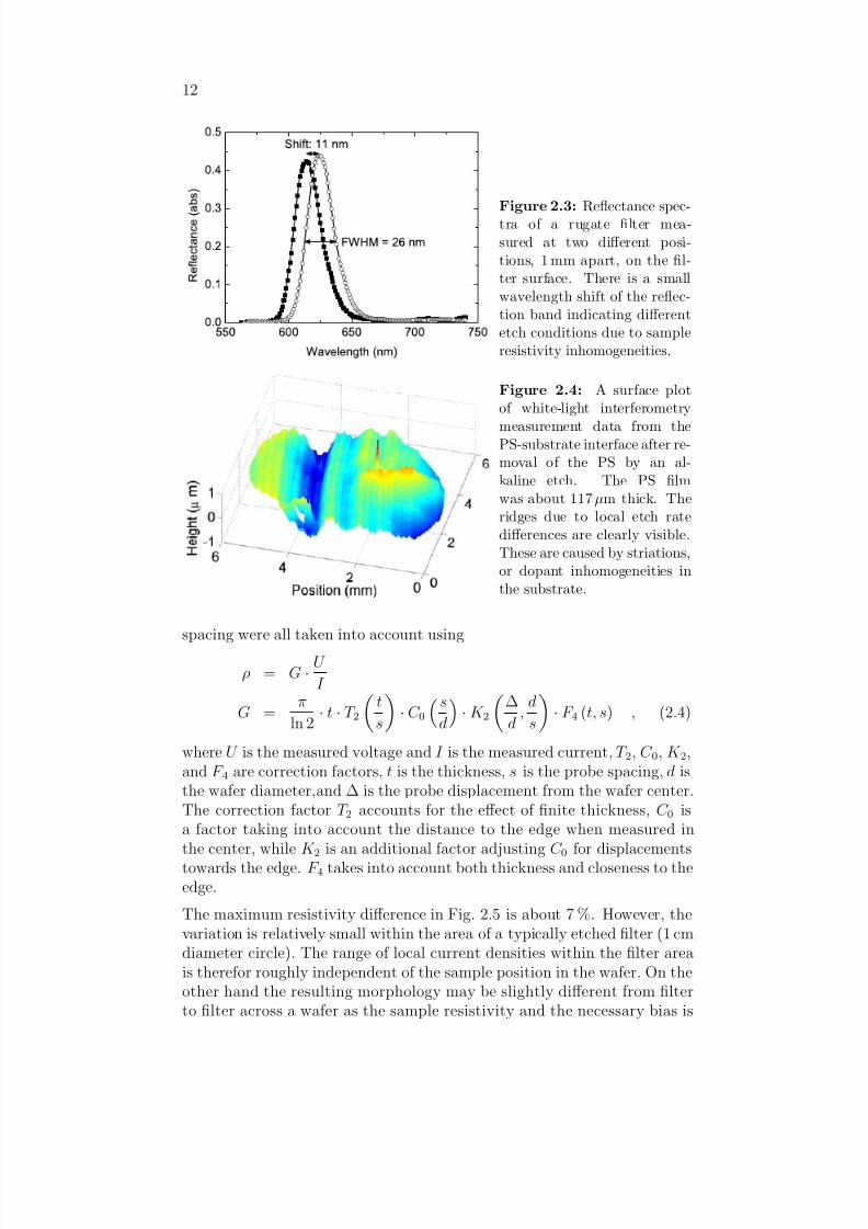
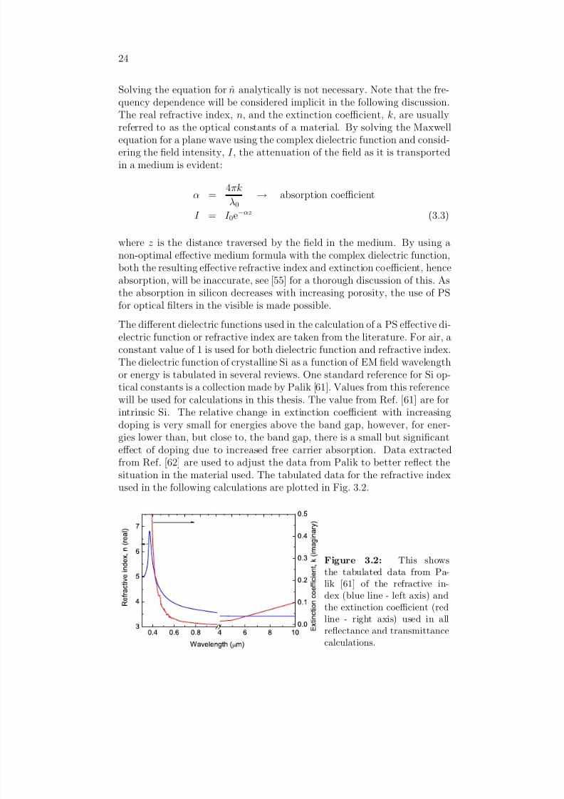
have been observed. In Fig. 2.3 the reflectance spectrum of a rugate opticalreflectance filter is measured. Details of the optical filters are discussed inChap. 3. Two measurements are made at different positions, 1 mm apart,on the filter surface. The reflection bands are shifted relative to each otherwhich indicates different conditions for interference. This is most likely dueto local differences in etch conditions, e.g. resistivity differences. Theseinhomogeneities are often visible on the surface of the optical filters, fab-ricated for this thesis, as slight deviations in color. These deviations takethe form of concentric circles often roughly coinciding with the center of the wafer. This may be seen in Paper V where a grayscale optical micro-
scope image clearly shows local differences in color. The difference in colorstems from porosity and layer thickness variations. By selectively removingthe PS by etching in a concentrated alkaline solution, e.g. 40% NaOH,the PS-substrate interface is revealed. Figure 2.4 shows a 3D surface plotof height data obtained by white-light interferometry from a test sample.One may clearly see ridges caused by spatially inhomogeneous etch rates.These ridges coincide with the color deviations. This is discussed more inPaper V. The spatial period with which these ridges occur along the radialdirection is in the 100 µm to 1 mm range.
The cause of these inhomogeneities in resistivity is most likely striations ,
or fluctuations in dopant concentration caused by the Si-ingot productionprocess. This is a well known problem in Si-technology and is thoroughlydiscussed in technical papers on Si wafer material quality, e.g. Ref. [38]gives a summary of semiconductor crystal growth specifically discussingstriation formation. The striation induced roughness has rather long spatialperiods and may in p+ samples give quite large surface height fluctuations.In lower doped p-type Si samples the striation induced roughness is lesspronounced [39]. This may be understood considering that the same dopantfluctuation relative to the average dopant concentration is likely to occur inboth highly doped and low doped Si, with the result that a different absolute
change in etch rate is observed. However, there will be interface roughnesswith smaller spatial periods (micro-roughness) which is more pronounced inp− samples than in p+ samples where this type of roughness is very small.This results in locally very good optical quality of p+ PS based optics,and promises good quality optics on larger area when striation effects arecontrolled.
The resistivity, ρ, does not only change at a local (µm) level, but also on awafer level. This has an impact on the reproducibility of filter fabrication.In Fig. 2.5 the result of a four-point-probe resistivity measurement acrossa typical wafer is shown. Standard geometrical correction factors from
Ref. [40] for thin, circular disks are used to calculate the resistivity. Distanceto wafer edge, orientation of the four-point-probe, wafer thickness and probe
8/12/2019 Graded Optical Filters
http://slidepdf.com/reader/full/graded-optical-filters 22/164
12
Figure 2.3: Reflectance spec-tra of a rugate filter mea-sured at two different posi-tions, 1 mm apart, on the fil-ter surface. There is a smallwavelength shift of the reflec-tion band indicating differentetch conditions due to sampleresistivity inhomogeneities.
Figure 2.4: A surface plotof white-light interferometrymeasurement data from thePS-substrate interface after re-moval of the PS by an al-kaline etch. The PS filmwas about 117µm thick. Theridges due to local etch ratedifferences are clearly visible.These are caused by striations,or dopant inhomogeneities in
the substrate.
spacing were all taken into account using
ρ = G · U
I
G = π
ln 2 · t · T 2
t
s
· C 0
s
d
· K 2
∆
d ,
d
s
· F 4 (t, s) , (2.4)
where U is the measured voltage and I is the measured current, T 2, C 0, K 2,and F 4 are correction factors, t is the thickness, s is the probe spacing, d is
the wafer diameter,and ∆ is the probe displacement from the wafer center.The correction factor T 2 accounts for the effect of finite thickness, C 0 isa factor taking into account the distance to the edge when measured inthe center, while K 2 is an additional factor adjusting C 0 for displacementstowards the edge. F 4 takes into account both thickness and closeness to theedge.
The maximum resistivity difference in Fig. 2.5 is about 7 %. However, thevariation is relatively small within the area of a typically etched filter (1 cmdiameter circle). The range of local current densities within the filter areais therefor roughly independent of the sample position in the wafer. On the
other hand the resulting morphology may be slightly different from filterto filter across a wafer as the sample resistivity and the necessary bias is

8/12/2019 Graded Optical Filters
http://slidepdf.com/reader/full/graded-optical-filters 23/164
13
different. Different resistivity and bias will likely change the depletion layerat the pore front which may change the resulting porosity or structure of thePS. There have been few, if any, systematic investigations of small changes
in wafer resistivity on the morphology of PS with optical applications inmind. A similar example to that in Fig. 2.3 of the effect of local resistivityvariations on filter characteristics is given by Lerondel et al. in Ref. [41].
Figure 2.5: The resistivitymeasured at different positionsacross a typical wafer used forPS etching. The measure-ments are obtained by a four-point-probe. The change inresistivity across the wafer is
significant and will affect thereproducibility of PS etching.Error bars show standard errorbased on three measurementsat different currents. Edge ef-fects are taken into account.The line is only a guide.
2.3.1.4 Drying
After etching, before the samples are taken out of the etch-bath, the bathwith the sample in it is rinsed out with ethanol. The sample is then takenout to air dry. Because of the size of the pores the capillary stress within thepores may be quite high. Depending on the size of the structure (porosity)and the surface tension of the liquid, cracking of the PS layer may occur.This limits the maximum porosity obtainable and also suggests a procedurefor drying [42, 43, 44]. When drying in air, a meniscus will always formin the pores which will result in a stress on the pore walls. This makes itimportant to have a very low surface tension liquid in the pores when drying.As suggested this may be done by rinsing out with pure ethanol which has
a lower surface tension than water (22 mJ/m2
compared to 72 mJ/m2
), analternative is to use pentane (with a surface tension of 14 mJ/m2). Pentane,however, is not water-soluble so the sample is usually rinsed in ethanol first.The best results, however, have been obtained by supercritical drying [44]in CO2 (>95 % porosity) where drying is performed above the supercriticalpoint of a liquid, usually CO2.
In the electrolyte and immediately after drying, the pore walls are mostlyH-terminated [34]. The hydrogen will be replaced by oxygen to form nativeoxide quite rapidly in air. This will change the properties of the PS overtime. Due to the large surface area of the PS the silicon-oxygen ratio may
be quite large resulting in a significant impact on the properties of PS. Formany applications this instability is not acceptable and several methods

8/12/2019 Graded Optical Filters
http://slidepdf.com/reader/full/graded-optical-filters 24/164
14
for surface passivation have been reported in the literature. Among theseare controlled oxidation by anodic or chemical oxidation, rapid thermaloxidation, capping of the PS layer by a dielectric or metal [45], thermal
nitridation or thermal carbonization [46].
2.3.2 Electrolyte properties
The electrolyte contents used for PS etching may vary substantially, how-ever, the electrolyte is generally based on aqueous HF. For all experimentsreported here, a 40 % aqueous HF has been used as the base. It is quitepossible to etch PS with this base diluted in water, however, to facilitate ex-traction of hydrogen bubbles formed during etching, ethanol is usually used
as a surfactant. Compared to water, ethanol has better wettability andlower surface tension which results in better infiltration in the nanometer-sized pores. Different additions or substitutions may be made to change theproperties of the electrolyte, e.g. to increase viscosity which is thought to in-fluence the PS-substrate interface roughness, glycerol may be added. Othersubstitutions include other organic solvents, especially dimethyl formamide(DMF) and dimethyl sulfoxide (DMSO) which result in p-type macro-PSfor certain parameters. A short overview of the different electrolyte com-positions reported in the literature is given in Ref. [32].
In papers II and III the effect of different electrolyte parameters is discussed.
Electrolytes containing different ratios of glycerol are used while measuringthe PS-substrate roughness evolution during etching. A comparison of roomtemperature and low temperature etch is also made. Both temperature andglycerol content seem to affect the interface roughness, however, the degreedepends on other parameters like HF concentration. For some parame-ter ranges the roughness decreases. It has been suggested [39, 47] thatthe reduction in roughness with decreasing temperature, down to -40 C,and increasing glycerol ratio is due to an increase in viscosity. Data fromRef. [48] suggest that a mix of water and glycerol (25 %) at 20 C has thesame viscosity as an equivalent mix of water and ethanol at about 12 C.
The exact viscosity values of the electrolytes will differ from these, but thecloseness of the tabulated data indicates that viscosity may be a criticalparameter. However, it is not obvious that an increase in viscosity itself isthe only reason why lower roughness is obtained. Especially in the case of low temperature etching, the reaction kinetics will most likely be affected.
The tentative explanation why a change in electrolyte viscosity affects theinterface roughness of PS, and also the refractive index inhomogeneity, isthat a situation closer to that of electropolishing is reached. During elec-tropolishing the holes diffuse faster to the interface than do active electrolytespecies (e.g. F−), which results in a ”guaranteed” availability of holes at
the surface. This has the consequence that ”peaks” are etched first, hencethe resulting surface is locally flat, where the extent of the locality depends

8/12/2019 Graded Optical Filters
http://slidepdf.com/reader/full/graded-optical-filters 25/164
15
on a characteristic length (e.g. diffusion length of holes). By reducing thediffusion of ions in the electrolyte during PS etching, the local differences of hole availability caused by an inhomogeneous resistivity will be reduced. In
the extreme case of ion diffusion controlled etching, the etch rate and poros-ity should be independent of resistivity. Some results of etching in glycerolcontaining electrolytes and low temperature etching will be presented inChapters 4 and 5.
2.4 Etch setup
There are usually two ways of setting up a sample for etching. These arenormally referred to as single etch cell and double etch cell. In the singleetch cell the sample is usually horizontal with a solid back contact, oftena Cu-plate, and the front side is in contact with a reservoir containing theelectrolyte. In the electrolyte there will be a Pt-cathode. In the double cellthe sample is vertically placed between two separate reservoirs containingthe electrolyte, both with Pt-electrodes, one working as cathode and oneas anode. Here the electrolyte reservoir works as a back side contact. Allsamples fabricated for this thesis were made with a single cell setup. Avertical single cell setup was used for some tests, but this resulted in etchrate and porosity inhomogeneities caused by H2 bubble formation and trap-ping. Vertical ridges were observed at the PS-substrate interface after PSstripping by concentrated NaOH which were most likely caused by bubbleinduced change in etch rate.
A sketch of a basic etch cell used in this thesis is shown in Fig. 2.6. Theback contact upon which the Si sample is placed is made of copper, on topof the sample, between the sample and the top part of the cell, is a sealingring or a sheet with an opening. The cell is made of Teflon or anothermaterial inert to HF. Several different variations of this basic cell havebeen used. The etch current is supplied by a computer-controlled Keithley
2400 sourcemeter. Etching is normally performed under galvanostatic, orconstant current, conditions, where current is the control parameter.
The biasing voltage was monitored during single PS layer fabrication todetect anomalies, such as significant changes in voltage due to leakage.In Fig. 2.7 a typical voltage monitored during an etching is shown. It isincluded here due to the curious curve shape. The plot contains surprisinglymany features considering the sample was etched with a constant current.There is a transient region in the beginning which may be ascribed to a buildup of charge before etching begins, e.g. due to an activation energy. Theirregular sawtooth pattern may be due to local oxide build-up and etching,
as in the current-burst model [36] or due to hydrogen bubbles interferingwith electrolyte flow.

8/12/2019 Graded Optical Filters
http://slidepdf.com/reader/full/graded-optical-filters 26/164
16
Figure 2.6: A sketch of thebasic etch cell used. The Sisample is placed on a Cu-platewhich is positively biased, ano-ring or silicon rubber sheet(HF-resistant) is placed on topof the sample before the toppart of the cell is fastened.The cell material is eitherTeflon or PVC. The electrolyteis filled into the reservoir anda Pt-electrode is placed in theelectrolyte. The Pt-electrodeis negatively biased. A com-
puter controlled current sourcecontrols the current/bias.
Figure 2.7: During etch-ing with constant current thevarying voltage is measured.There is a transient period atthe start which after a few sec-onds goes over into an irregu-lar saw tooth pattern. This os-
cillation may be linked to ox-ide build up and etch in thepores, however, this is not wellunderstood.
2.4.1 Optimizing the etch setup
The geometry of the etch cell will influence the current density distributionin the sample. In an effort to optimize the etch cell for homogeneous etch-ing, a simplified 2D finite element method (FEM) calculation was done inFemlab [49] to understand the current density distribution. Three factorswere tested, the geometry of the top part of the cell, i.e. the electrolytereservoir, the size of the back-contact and the influence of an opening in theback-contact. The sketch in Fig. 2.8b) shows the cell geometries tested. Thewide, funnel-shaped cell has a top opening of 2 cm diameter. The sampleopening for both designs is 1 cm diameter, while the height is 2 cm for thefunnel design and 4 cm for the straight reservoir design. For the FEM calcu-lations, an electrostatic model described in Cartesian coordinates was used.The geometries consist of the sample, with the measured resistivity value,electrolyte, with a measured resistivity value and an isolating cell material.
Only the potential and current density distributions based on different ge-ometries and voltages were considered in the calculation, disregarding all

8/12/2019 Graded Optical Filters
http://slidepdf.com/reader/full/graded-optical-filters 27/164
17
chemical and electrochemical effects. The results from these calculationsare rough approximations as the potential drop across the Helmholz-layerclose to the Si-surface will normally be quite large. This probably results in
an overestimate of the significance of the placements of the electrodes andof the cell geometry, however, the trends shown should still be valid.
Figure 2.8a) shows the current density distribution at a depth of 20 or 50 µmin the sample from the center out to the side of the etched area. The topplot shows a comparison between the two cell geometries. There is a clearinhomogeneity of the current density when the wide cell is used. In this casethe modeled samples had back-contacts covering the whole back-side andthe current density was calculated for a depth of 20 µm. The middle plotshows a comparison between two samples having back contacts with thesame size as the front opening. One of the samples has a 0.5 mm opening in
the center of the back contact to make possible interference measurements aswill be described in Sec. 4. Current densities were calculated for a depth of 50 µm. It is clear that the influence of the back contact opening is significantat this depth. The selected opening size is the minimum obtainable due tomechanical constraints in the fabrication of the back plate.
The bottom plot shows a comparison of two samples with wide and narrowback contacts, i.e. the back contact has the same size as the front opening.The homogeneity of the current density is significantly better in the case of the narrow back contact. The current density distribution close to the edgeof the electrolyte in the two cases may also be seen in the cross-sections
shown in Fig. 2.9. In the case of the narrow back contact, the currentdensity distribution will be more homogeneous with depth also. As can beseen in Fig. 2.9, the current spreads out more towards the back contact inthe wide contact case. There will be a certain under-etching due to thespreading of current in the sample. The effect of this is a slight decrease incurrent density with depth which may be compensated for by an increasein the current with time.
2.5 Etch setup for graded filter etching
To make optical filters where the filter characteristics are dependent on theposition on the filter, a voltage was set up between two contacts, 1.2 cmapart, on the back side of the sample. This resulted in a position dependentcurrent density during etching with in turn gave a change in refractive indexmodulation with depth at different positions. Some results on etched filterstructures using this effect are presented in Paper V. The etch cell usedfor this is schematically shown in Fig. 2.10 and is basically the same as inFig. 2.6 with a difference in the back contact. Two thin Cu-sheets with aspacing of about 12 mm were used instead of the single Cu-plate. A FEM
simulation of the current density in the sample at a depth of 2 µm for atypical set of parameters is shown in Fig. 2.11. The model used is similar

8/12/2019 Graded Optical Filters
http://slidepdf.com/reader/full/graded-optical-filters 28/164
18
a) b)
Figure 2.8: a) A comparison of current density profiles is shown for dif-ferent etch cell and back contact geometries from FEM calculations of a 2Delectrostatic model in Femlab. The top figure shows profiles calculated at asubstrate depth of 50 µm while the two figures below are calculated at 20µm.The profiles are plotted from the center of the etch area to the edge of thereservoir. The top figure shows a comparison between a cell with a funnelshaped reservoir and a back contact wider than the electrolyte contact area(curve A, the geometry to the right) with a tall and narrow reservoir geom-etry with a back contact the same size as the front contact area (curve B,the geometry to the left). The middle figure shows a comparison of two pro-files obtained with the narrow geometry with the same narrow back contact(curve C) save for a 0.5 mm opening for in situ IR reflectance measurements(curve D). The bottom figure shows a comparison between a narrow (curveC) vs. wide (curve E) back contact with the tall reservoir geometry. Figureb) shows the cell geometries.
to that in Sec. 2.4.1 The potential difference across the sample in this caseis 0.2 V while the potential difference between the back contact with thehighest potential and the Pt-cathode is 2 V. The conductivities used for thematerials in the simulation are realistic, although not necessarily measured.

8/12/2019 Graded Optical Filters
http://slidepdf.com/reader/full/graded-optical-filters 29/164
19
−5.4 −5.2 −5 −4.8 −4.6 −5.4 −5.2 −5 −4.8 −4.6
−5
−4
−3
−2
−1
0
1
2
Position (10−1
mm)
P o s i t i o n ( 1 0 − 1 m
m )
Substrate
Electrolyte reservoir
Back−contact
Reservoir wall
a)
−5.4 −5.2 −5 −4.8 −4.6 −5.4 −5.2 −5 −4.8 −4.6
−5
−4
−3
−2
−1
0
1
2
Position (10−1
mm)
P o s i t i o n ( 1 0 −
m m )
Back−contact
Substrate
Reservoir wall Electrolyte reservoir
b)
Figure 2.9: Screen shots from a Femlab calculation showing the currentdensity distribution and direction for the narrow (a) and wide (b) back con-tact with a narrow electrolyte reservoir. The effect of the back contact geom-etry is larger towards the edges of the electrolyte contact area and towardsthe back contact.
Figure 2.10: The etch cell forthe graded samples is basicallythe same as in Fig. 2.6. How-ever, the back contact is splitin two with a gap between.A constant bias is applied be-tween these two contacts. Oneof the contacts is connected tothe computer controlled cur-rent source.
Figure 2.11: The cur-rent density profile calculated20µm into the sample fromthe electrolyte-sample inter-face. The two back contactsare biased to 2 and 1.8 V whilethe Pt electrode is grounded.The calculation is made witha 2D model in Femlab. Inthis calculation the electrolyteis assumed to be a conducting
material and the electrochem-istry is disregarded.

8/12/2019 Graded Optical Filters
http://slidepdf.com/reader/full/graded-optical-filters 30/164

8/12/2019 Graded Optical Filters
http://slidepdf.com/reader/full/graded-optical-filters 31/164
Chapter 3
Thin-film calculations
For many years multilayer dielectric thin film optical interference filtershave been used [50]. Obtaining interference effects by using layers of opticalthickness in the order of the wavelength of the light of interest have beenexploited in many applications. In this thesis multilayer and inhomogeneousstructures in PS are used to some extent to control light. Interferenceeffects with electromagnetic (EM) fields are obtained only with very specificstructures. Layer optical and physical thicknesses or layer refractive index
modulation periods must be in the order of the wavelength at which onewants interference. In the visible and near infrared wavelength regions thistranslates to structures with elements down to below 100 nm with strictdemands on size accuracy and definition. It is very important to understandthe optical properties of the material, which in this case is PS, to be ableto design such interference systems. In the first section the correspondencebetween the porous structure of PS and refractive index will be discussed.
As the correspondence between PS fabrication parameters and obtainedstructures is not trivial, a detailed knowledge of the intended structures and
their optical response is needed to be able to understand the actual responsefrom fabricated structures. The background for calculation of interferencefilter responses will be presented in Sec. 3.2. In addition to the most ba-sic multilayer optical system a few physical effects are taken into account.These include dispersion, absorption and interface roughness. The incorpo-ration of interface roughness into optical response calculations is describedin Sec. 3.3. This will be used both in optical filter calculations as well asin the analysis of in situ laser reflectance measurements described in detailin Chap. 4. In the last section, different multilayer and inhomogeneousrefractive index optical filter structures will be presented together with
calculations of optical responses based on the methods described. Thesestructures are experimentally realized and presented in Chap. 5.
21

8/12/2019 Graded Optical Filters
http://slidepdf.com/reader/full/graded-optical-filters 32/164
22
3.1 Effective medium theory
A porous medium will exhibit different optical properties than the same
material in bulk. If the typical feature sizes (e.g. pore size) are much smallerthan the wavelengths of the incident electromagnetic field, the field in theporous medium encounters an effective dielectric function. This effectivedielectric function is dependent on the dielectric functions of both the bulkmaterial and the filling material (e.g. air) in a ratio controlled by, amongstother parameters, the porosity.
The theory describing the dielectric function of the mixed media is re-ferred to as effective medium theory. There are several prominent effectivemedium formulas, e.g. Bergman [51], Maxwell-Garnett [52], Looyenga [53]and Bruggeman [54]. The main difference between these formulas lies in
how the microtopology of the pores are taken into account. The opticalresponse of a porous medium will change with the degree of ”connected-ness” (percolation strength) of the network and the sizes of the segments of material left in the medium. The dependence on microtopology makes theproblem of finding a correspondence between porosity and effective dielec-tric function non-trivial. Maxwell-Garnett, Looyenga and Bruggeman allassume certain microtopologies resulting in a more or less limited validitywhen considering the effective dielectric function of PS as the microtopol-ogy is greatly dependent on formation parameters. An example of this isreported by Setzu et al. [47] where the same porosity obtained by different
formation parameters gives significantly different refractive indexes.The Bergman formula is general and takes into account the microtopologyby a spectral density function, however, this function is usually not knownand must be expressed specifically for all the different microtopologies of different PS films, hence this approach is quite involved. The use of effec-tive medium theory to describe the optical properties of PS is extensivelydiscussed by Theiß in Ref. [55, 56]. Figure 3.1 is taken from [56] and showsa comparison of several different effective medium formulas.
Figure 3.1: Comparison of different effective medium for-mulas giving refractive indexas a function of porosity. Theplot is taken from Ref. [55].
Notably the most cited effective medium formula in association with PS

8/12/2019 Graded Optical Filters
http://slidepdf.com/reader/full/graded-optical-filters 33/164
23
is the Bruggeman formula, often referred to as the Effective Medium Ap-proximation (EMA). The popularity of the EMA is based on a paper byAspnes [57] where spectroscopic ellipsometry measurements were performed
on rough amorphous Si. The model describing the roughness which gavethe best fit was the EMA. The EMA is also used in this thesis for all re-fractive index-porosity calculations. The samples presented in this thesisshould have a narrow range of topologies caused by a narrow range of sub-strate resistivities and a relatively narrow range of HF concentrations in theelectrolyte. Any error introduced by the choice of the EMA as an effectivemedium formula will then be systematic and may be easily adjusted for.The Bruggeman formula is given by:
p M − eff M + 2eff
+ (1 − p) − eff + 2eff
= 0 (3.1)
where p is the porosity, , M and eff are the dielectric functions of theembedded material (Si), the host material (air/vacuum) and the effectivemedium (PS) respectively.
By using the EMA for all porosities and PS structures, it is clear from thepreceding discussion that for most situations there will be some error in thecalculation due to different microtopologies. From the literature it seemsthat this error is small and, in most cases, tolerable for the applications andmeasurements in mind. Some papers [58, 59] suggest that the Looyenga for-
mula better describes the dielectric function of highly porous meso-porousPS. We may calculate the effect of using different effective medium formulason the optical response of a simple Bragg reflector. We see from Fig. 3.1that there is a maximum difference in refractive index of about 0.08 for80 % porosity, or equivalently a difference in porosity of about 4.5 % for arefractive index of 1.3. Given a Bragg reflector designed for a reflectionband around a wavelength of 600 nm, the change introduced by going fromthe Bruggeman to the Looyenga effective medium formula will result in ashift of the reflection band (given unchanging layer thicknesses) of about40 nm. This error may be critical for some types of applications, hence thechoice of model, and possible corrections, must be kept in mind.
If we use a complex, frequency dependent dielectric function (dispersivemedia), (ω), the absorption in the material will be taken into account.The effective medium models may be used with these complex values. Thecomplex dielectric function is defined in the following as well as its relationto the complex refractive index, n(ω). We assume for all calculations thatthe materials are non-magnetic, i.e. the magnetic permeability, µ, equals 1(from [60]):
(ω) = r(ω) + ii(ω)
n(ω) = n(ω) + ik(ω)n(ω) =
(ω)µ (3.2)
8/12/2019 Graded Optical Filters
http://slidepdf.com/reader/full/graded-optical-filters 34/164
24
Solving the equation for n analytically is not necessary. Note that the fre-quency dependence will be considered implicit in the following discussion.The real refractive index, n, and the extinction coefficient, k, are usually
referred to as the optical constants of a material. By solving the Maxwellequation for a plane wave using the complex dielectric function and consid-ering the field intensity, I , the attenuation of the field as it is transportedin a medium is evident:
α = 4πk
λ0
→ absorption coefficient
I = I 0e−αz (3.3)
where z is the distance traversed by the field in the medium. By using a
non-optimal effective medium formula with the complex dielectric function,both the resulting effective refractive index and extinction coefficient, henceabsorption, will be inaccurate, see [55] for a thorough discussion of this. Asthe absorption in silicon decreases with increasing porosity, the use of PSfor optical filters in the visible is made possible.
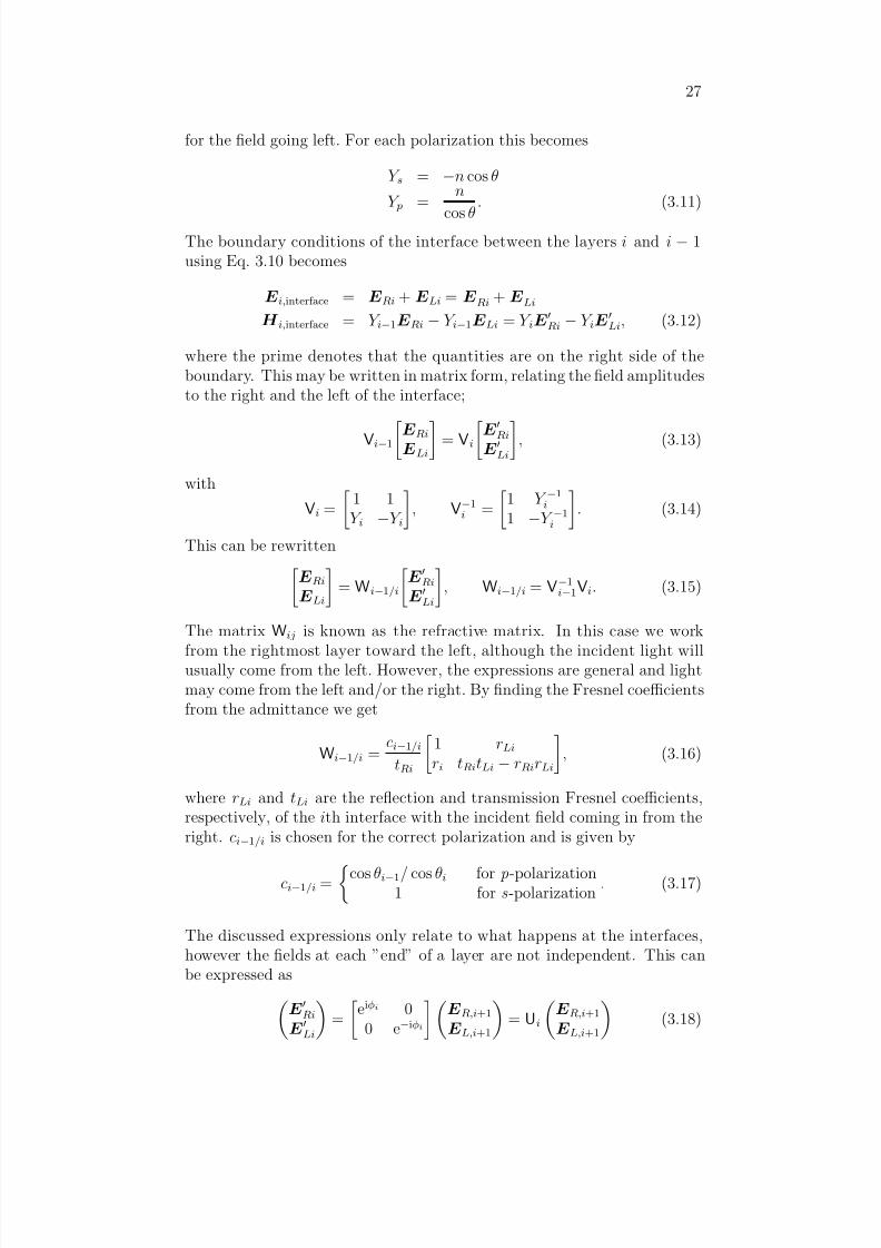
The different dielectric functions used in the calculation of a PS effective di-electric function or refractive index are taken from the literature. For air, aconstant value of 1 is used for both dielectric function and refractive index.The dielectric function of crystalline Si as a function of EM field wavelengthor energy is tabulated in several reviews. One standard reference for Si op-
tical constants is a collection made by Palik [61]. Values from this referencewill be used for calculations in this thesis. The value from Ref. [ 61] are forintrinsic Si. The relative change in extinction coefficient with increasingdoping is very small for energies above the band gap, however, for ener-gies lower than, but close to, the band gap, there is a small but significanteffect of doping due to increased free carrier absorption. Data extractedfrom Ref. [62] are used to adjust the data from Palik to better reflect thesituation in the material used. The tabulated data for the refractive indexused in the following calculations are plotted in Fig. 3.2.
Figure 3.2: This showsthe tabulated data from Pa-lik [61] of the refractive in-dex (blue line - left axis) andthe extinction coefficient (redline - right axis) used in allreflectance and transmittance
calculations.

8/12/2019 Graded Optical Filters
http://slidepdf.com/reader/full/graded-optical-filters 35/164
25
3.2 Reflectance calculation
Two equivalent ways of mathematically defining an optical multilayer sys-
tem will be presented here. Both of these methodologies will be describedand used as they have different advantages. For these calculations we willassume that the material is homogeneous for each layer, i.e. the refractiveindex is constant and identical in all directions: n(x,y,z ) = n, and that theplanes are parallel.
3.2.1 Characteristic matrix
A good derivation of the characteristic matrix approach is given
in [63](Chapter 1). A short summary will be given in the following.Each layer in a multilayer system may be represented by a ”characteristicmatrix”, M, describing its optical properties. To obtain the optical charac-teristics of a stack of layers, a matrix multiplication is performed with thecharacteristic matrixes of all layers. The normal to the stacks is along thez −axis. To relate the EM field vectors on both sides of a stack of i numberof layers we get:
Q0 = M1M2 · · ·MiQ = MQ , (3.4)
where Q and Q0 contain the x- and y-components of the EM field at positionz and z 0 = 0, respectively. The characteristic matrix describing one layer
in a multilayer system for a transverse electric (TE) field (s-polarized) isgiven by
Mi(di) =
cos(k0nidi cos θi) − i
pisin(k0nidi cos θi)
−i pi sin (k0nidi cos θi) cos (k0nidi cos θi)
. (3.5)
Here pi =
(i/µi)cos θi and k0 = 2π/λ0, where λ0 is the incident wave-length in vacuum, and di is the layer thickness. To obtain the same charac-teristic matrix in the case of a transverse magnetic (TM) field (p-polarized),
q i =
(µi/i)cos θ is used instead of pi. With the components of the totalcharacteristic matrix of the stack denoted by
M =
m11 m12
m21 m22
, (3.6)
the reflection and transmission coefficients of the system are then given by
r = (m11 + m12 pl) p1 − (m21 + m22 pl)
(m11 + m12 pl) p1 + (m21 + m22 pl) ,
(3.7)
t = 2 p1
(m11 + m12 pl) p1 + (m21 + m22 pl) . (3.8)

8/12/2019 Graded Optical Filters
http://slidepdf.com/reader/full/graded-optical-filters 36/164
26
The reflectivity and transmissivity are given by
R = |r|2 ,
T = p
l p1
|t|2
, (3.9)
where p1 and pl are for the first and last layers, respectively. A sketch of thedescribed layered system with notation for both the characteristic matrixapproach and the admittance matrix approach described below is shown inFig. 3.3
Figure 3.3: The system de-scribed in the text, with theused notation. Usually light isconsidered to travel from leftto right.
To calculate the reflection of transmission spectrum, the equations in Eq. 3.9
must be calculated for the wavelength range of interest. This description of the transfer matrix method is the easiest to implement, but also the leastflexible. The alternative method presented below gives identical results withthe same assumptions, but has the added advantage of easy implementationof interface roughness.
3.2.2 Admittance matrix
A different approach to describe an optical system of dielectric layers is tostart with the optical admittance. The description presented below is taken
from Knittl [64] and Mitsas and Siapkas [65]. It easily facilitates the directintroduction of the Fresnel coefficients of the interfaces, hence the additionof factors describing interface roughness as will be shown. The notationis such that the ith interface corresponds to the ith layer just to the rightof the interface and the interfaces are numbered left to right. From theboundary conditions of an interface between two media, the characteristicoptical admittance of a medium may be defined as
Y = H tR
E tR= −
H tL
E tL, (3.10)
where H tR and E tR are the tangential vector components of the incidentmagnetic and electrical field respectively, both going right. The same goes
8/12/2019 Graded Optical Filters
http://slidepdf.com/reader/full/graded-optical-filters 37/164
27
for the field going left. For each polarization this becomes
Y s = −n cos θ
Y p = n
cos θ . (3.11)
The boundary conditions of the interface between the layers i and i − 1using Eq. 3.10 becomes
E i,interface = E Ri + E Li = E Ri + E Li
H i,interface = Y i−1E Ri − Y i−1E Li = Y iE
Ri − Y iE
Li, (3.12)
where the prime denotes that the quantities are on the right side of theboundary. This may be written in matrix form, relating the field amplitudes
to the right and the left of the interface;
Vi−1
E Ri
E Li
= Vi
E
Ri
E
Li
, (3.13)
with
Vi =
1 1Y i −Y i
, V−1
i =
1 Y −1
i
1 −Y −1i
. (3.14)
This can be rewritten
E RiE Li = Wi−1/iE
Ri
E
Li, Wi−1/i = V−1
i−1Vi. (3.15)
The matrix Wij is known as the refractive matrix. In this case we workfrom the rightmost layer toward the left, although the incident light willusually come from the left. However, the expressions are general and lightmay come from the left and/or the right. By finding the Fresnel coefficientsfrom the admittance we get
Wi−1/i = ci−1/i
tRi
1 rLiri tRitLi − rRirLi
, (3.16)
where rLi and tLi are the reflection and transmission Fresnel coefficients,respectively, of the ith interface with the incident field coming in from theright. ci−1/i is chosen for the correct polarization and is given by
ci−1/i =
cos θi−1/ cos θi for p-polarization
1 for s -polarization . (3.17)
The discussed expressions only relate to what happens at the interfaces,however the fields at each ”end” of a layer are not independent. This canbe expressed as
E Ri
E
Li
=
eiφi 00 e−iφi
E R,i+1
E L,i+1
= Ui
E R,i+1
E L,i+1
(3.18)

8/12/2019 Graded Optical Filters
http://slidepdf.com/reader/full/graded-optical-filters 38/164
28
Ui is called the phase or propagation matrix. The phase-shift, φi, is givenby
φi = 2π
λ0
nidi cos θi (3.19)
To obtain the total field transformation of a layered system, with layersfrom 1 to i, the matrices are multiplied to give, in the general case:
E R1
E L1
= W01U1W12U2W23 . . . Wi−1,iUiWi,i+1
E
R,i+1
E
L,i+1
= S
E
R,i+1
E
L,i+1
, (3.20)
Here S is the system transfer matrix, and
S =
s11 s12
s21 s22
. (3.21)
The system transfer matrix transforms the tangential components of theincident fields, from both sides of the layer stack, at one end of the stackto the exiting field at the other end. To find the Fresnel coefficients of thesystem we use the definitions which gives
rRi = E Li
E Ri, tRi =
E
Ri
E Ri,
rLi = E
Ri
E
Li
, tLi = E Li
E
Li
.
(3.22)
Together with Eq. 3.20 we get for the system:
rR = s21
s11
, tR = 1
s11
,
rL = −s12
s11
, tL = det S
s11
.
(3.23)
By using the complex refractive index, absorption will be taken account of with this method also.
As will become clear in the next section, it is quite simple to add roughnesscoefficients to this description. These coefficients are added as pre-factorsto the Fresnel coefficients and takes into account the roughness at eachinterface, given certain assumptions.
3.3 Roughness calculation
Roughness in the context of this thesis is based on the height function of theinterface of interest, h(x, y). We assume that the xy plane is parallel to the

8/12/2019 Graded Optical Filters
http://slidepdf.com/reader/full/graded-optical-filters 39/164
29
sample surface. This function describes the deviation of the interface froma perfectly flat surface. It is more practical to work with a single numberfor the roughness than the height function, so we define an interface height
average. It is assumed that the interface height function is isotropic, henceit is enough to find the average in one direction, which may then be givenby
a = 1
L
L0
h(x)dx. (3.24)
The value used for roughness characterization is usually the root meansquare (rms) value of the height function, σ, given by:
σ = 1
L L
0
(h(x) − a)2 dx. (3.25)
L is a characteristic distance, e.g. scan length. This length is quite im-portant as average values (large radius bending of surface) and rms values(different spatial period of roughness/fluctuations) may change consider-ably with the scale of L. Roughness may be measured by several methods,i.e. stylus profilometry, white light interferometry or optical scattering (dif-fuse and specular). Pertaining to this thesis, the consequences of roughnesson the optical field is of most importance, both for determining roughnessand also for evaluating the effect of roughness. A method to measure theroughness evolution in situ during PS etching, based on the theory described
here, has been developed and will be presented in detail in Chapter 4 andin Paper I.
3.3.1 Davies-Bennett theory
A much used theory describing the effects of a randomly rough surface onthe propagation of an EM field is the theory described by Bennett andPorteus [66]. This theory is based on work by Davies [67] who modeledthe scattering of perfectly conducting random rough surfaces. Bennett and
Porteus modified this theory to include materials of finite conductivity,hence the theory is often referred to as Davies-Bennett theory. These papersonly discuss normal incidence reflection from rough surfaces, but the theoryis easily expanded to include transmission [68] as well as EM fields incidentat oblique angles.
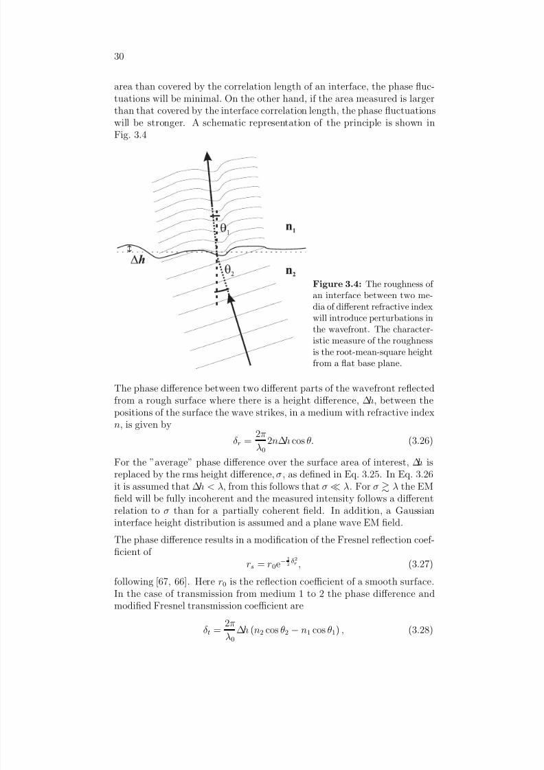
The principle is that of the rough surface introducing a fluctuation in thereflected or transmitted phase of the field such that when the field intensityis measured there will be destructive interference between different partsof the field front. It should be noted that the effect of roughness on theintensity depends on the area which is illuminated. Interface height fluctu-
ations typically have a correlation length describing over what length scalesthe fluctuations occur. If the EM field intensity measured is from a smaller
8/12/2019 Graded Optical Filters
http://slidepdf.com/reader/full/graded-optical-filters 40/164
30
area than covered by the correlation length of an interface, the phase fluc-tuations will be minimal. On the other hand, if the area measured is largerthan that covered by the interface correlation length, the phase fluctuations
will be stronger. A schematic representation of the principle is shown inFig. 3.4
Figure 3.4: The roughness of an interface between two me-dia of different refractive indexwill introduce perturbations inthe wavefront. The character-istic measure of the roughnessis the root-mean-square heightfrom a flat base plane.
The phase difference between two different parts of the wavefront reflectedfrom a rough surface where there is a height difference, ∆h, between thepositions of the surface the wave strikes, in a medium with refractive indexn, is given by
δ r = 2π
λ0
2n∆h cos θ. (3.26)
For the ”average” phase difference over the surface area of interest, ∆h isreplaced by the rms height difference, σ , as defined in Eq. 3.25. In Eq. 3.26it is assumed that ∆h < λ, from this follows that σ λ. For σ λ the EM
field will be fully incoherent and the measured intensity follows a differentrelation to σ than for a partially coherent field. In addition, a Gaussianinterface height distribution is assumed and a plane wave EM field.
The phase difference results in a modification of the Fresnel reflection coef-ficient of
rs = r0e−1
2δ2r , (3.27)
following [67, 66]. Here r0 is the reflection coefficient of a smooth surface.In the case of transmission from medium 1 to 2 the phase difference andmodified Fresnel transmission coefficient are
δ t = 2πλ0
∆h (n2 cos θ2 − n1 cos θ1) , (3.28)

8/12/2019 Graded Optical Filters
http://slidepdf.com/reader/full/graded-optical-filters 41/164
31
ts = t0e−1
2δ2t . (3.29)
This results in the following adjusted Fresnel coefficients which will be used
in simulations with the proposed methods in 3.2:
rRi = r0Ri exp
−2 (2πσini−1 cos θi−1/λ0)2
= αr0
Ri
rLi = r0Li exp
−2 (2πσini cos θi/λ0)2
= βr0
Li
tRi = t0Ri exp−1/2 (2πσi/λ0)2 (ni cos θi − ni−1 cos θi−1)2
= γt0Ri
tLi = t0Li exp−1/2 (2πσi/λ0)2 (ni−1 cos θi−1 − ni cos θi)
2
= γt0Li(3.30)
The optical power lost in the specular direction (both reflected and trans-mitted) because of roughness is regained in the diffuse scattering, i.e. scat-tering in other directions than specular. For the calculations done in thisthesis, only specular reflection and transmission is considered.
As the roughness, as discussed above, will be incorporated into a calcula-tion of reflectance/transmittance of multilayer structures, the correlationof interface profiles from one layer to another must be considered. It isreasonable to assume, due to the nature of PS fabrication, that there willbe a certain degree of correlation of roughness between layers. This wouldsomewhat decrease the effect of interface roughness compared to fully un-correlated interface profiles. However, the refractive index contrast between
layers is smaller than between the layer stack and the substrate which resultsin a greater effect of roughness at the PS-substrate interface than elsewhere.This is especially true for rugate filters where the refractive index contrastbetween layers is very small. Due to the simplicity of incorporation and therelative small difference the two options should make on the outcome, onlythe effect of fully uncorrelated interface roughness scattering/incoherenceis incorporated into the calculations.
3.4 Optical multilayer interference filters
3.4.1 Discrete, homogeneous layers
The simplest type of a multilayer thin film interference filter is a Braggreflector or a Bragg stack. It is based on a stack of paired layers, whereeach layer satisfies the Bragg condition,
nd = λ0/4 , (3.31)
with one layer having a low refractive index, nL, and the other layer havinga high refractive index, nH . A compact way of denoting the design is
HLHLHL...HL = (HL)i, with i being the number of pairs. The thicknessof the layer is d while λ0 is the wavelength of the incident EM wave in

8/12/2019 Graded Optical Filters
http://slidepdf.com/reader/full/graded-optical-filters 42/164
32
vacuum for which the maximum reflection will occur (design wavelength).Plane waves are assumed. This condition results in the reflected EM waveat the design wavelength constructively interfering in each layer and one
may reflect up to 100 % of the incident energy. The reflectance of a Braggreflector designed for a maximum reflectance at a wavelength of 1550 nmis shown in Fig. 3.5. In this case the stack consists of 10 layer pairs. Thematerial used is 50% and 80% porosity PS. All the calculations in thefollowing are based on the discussion in Sec. 3.2.
By increasing the contrast, i.e. the difference between the high and low re-fractive index, one may widen the reflected wavelength band. By increasingthe number of pairs in the stack, the reflection band edges will be sharper,as shown in Fig. 3.6. The stack is similar to that used in Fig. 3.5 excepta stack of 20 layer pairs was used. In both cases interface roughness, ab-
sorption and dispersion were disregarded. In most applications the idealreflector would be one where there is no reflection outside the band and100 % reflection within the band, i.e. a square reflection band.
Figure 3.5: Calculated reflectionspectrum of a Bragg reflector con-sisting of 10 layer pairs of 50 % and80 % porosity on a Si-substrate, thedesigned band is centered at a wave-
length of 1550 nm. Absorption, dis-persion and interface roughness arenot taken into account.
Figure 3.6: The design is com-parable to Fig. 3.5 except it con-sists of 20 layer pairs. Note thesharper band edges due to the in-creased number of layers. Absorp-
tion, dispersion and interface rough-ness are not taken into account.
The layers may be combined in any way, and many types of filters arepossible for many different uses. Anti-reflection coatings, polarizers, beam-splitters and band-pass filters may all be made by use of multilayer thinfilms. A Fabry-Perot band-pass filter is obtained if a spacer layer is in-troduced between two mirrored Bragg stacks. An example of this is thestructure (HL)i(LH ) j where the spacer consists of two L layers. This will
give a sharp resonance peak in the transmission spectra at the design wave-length.

8/12/2019 Graded Optical Filters
http://slidepdf.com/reader/full/graded-optical-filters 43/164
33
3.4.2 Inhomogeneous layers
The types of optical multilayer filters mentioned above are based on dis-
crete layers with homogenous refractive indexes and uniform thicknesses.It is possible, however, to generalize this to layers of controlled inhomoge-neous refractive index (both in depth and laterally). The process of contin-uously varying the refractive index of a layer with depth has until recentlybeen quite difficult. There are a few systems in which this is possible,such as plasma enhanced chemical vapor deposition of silicon oxynitride(SiOxNy) [69] where the refractive index changes with the stoichiometrywhich may be controlled with the ratio of formation gases. Other meth-ods include magnetron sputtering deposition with variable control of theformation gases [70] or deposition of quasi-inhomogeneous layers consist-
ing of many, very thin, homogeneous layers [71], glancing angle depositionto fabricate porous structures of depth dependent porosity [72, 73], andcodeposition of two oxides by evaporation [74]. However these systems areusually relatively expensive and complex and have a limited range of re-fractive indexes available.
With PS, a practically obtainable refractive index contrast in the NIR of about ∆n = 3.0 − 1.2 = 1.8 is possible and the method is comparablystraightforward and inexpensive. This flexibility of PS enables both noveloptical elements in intimate connection to Si technology as well as a testingbed for novel stand-alone optical filters. There are several arguments for
fabricating optical elements with inhomogeneous refractive index. By avoid-ing internal interfaces, the structure becomes mechanically more stable, e.g.
against scratches, and the probability of delamination is reduced. Fewer in-terfaces also result in a decrease in the scattering of the EM field within thestructure. One typical use of inhomogeneous refractive index layers is inanti-reflection coatings. Another possibility is varying the refractive indexsinusoidally with layer depth. This results in a rugate reflection filter. Therefractive index profile is given by
n (z ) = na + n p
2 sin
2πz
nad + φ , (3.32)
with the design wavelength equal to 2nad. Here na is the average of themaximum (nH ) and minimum (nL) refractive index used in the layer, n p isthe peak-to-peak difference between minimum and maximum values and dis the physical thickness period of the refractive index sine profile, z is thedepth in the layer and φ is the phase. The resulting spectral characteristicsof the filter are quite similar to a Bragg reflector. However, in the case of small n p, there are no higher order harmonics (at normal incidence) and byfurther exploiting a continuous variation in refractive index one may reducesidebands as well. To avoid higher harmonics in the reflectance spectrum for
larger modulations in the refractive index profile, Eq. 3.32 must be modifiedso that the exponential of the sinusoidally modulated refractive indexes are

8/12/2019 Graded Optical Filters
http://slidepdf.com/reader/full/graded-optical-filters 44/164
34
obtained [29, 75]:
n (z ) = exp ln nH + ln nL
2
+ ln nH − ln nL
2
sin2πz
nad
+ φ . (3.33)
This ensures that the optical thickness of the positive sine half is not largerthan the negative sine half, hence there will a be perfect match betweenthe structure and the incident EM wave. By using Eq. 3.32 with relativelylarge n p there will be higher order harmonics in the reflectance/transmissionspectrum. Similar to Bragg reflectors the reflection band of a rugate filterwill widen with a greater refractive index contrast (nL to nH ) and thenumber of periods gives the ”quality” of the reflection band.
By adding an index matching region between the filter and the main inter-faces of air and substrate, the ”base” reflectance is reduced. By apodizing,i.e. adding a windowing function to the refractive index profile, the side-bands are reduced. The index matching consists of a smooth transition inthe refractive index between two media, i.e. from air to the filter ”medium”,and from the filter to the substrate, where the filter refractive index is con-sidered to be na. There are many possible gradient functions, but onewhich has been shown to give good results is the 5th order polynomial(quintic) [75, 76]:
n = nL + (nH − nL)(10t3 − 15t4 + 6t5), t ∈ [0, 1], (3.34)
where t is a normalized parameter proportional to depth. There are manywindowing functions that may be used for apodization, e.g. triangular,sine, Gaussian, polynomial and other windowing functions used in signalanalysis.
Figure 3.7 shows the calculated reflectance of a rugate filter designed formaximum reflection at 1550 nm. In this case, to show the ideal reflectance,the outer and substrate media have the same refractive index as the filteraverage index and no dispersion, absorption or roughness is taken into ac-count. The filter consists of 20 periods with no apodization. Maximumand minimum refractive index correspond to a porosity of 50 % and 80 %
respectively. Compared to Figs. 3.5 and 3.6 the higher order harmonics areclearly gone. By adding apodization, the sidebands are completely removedwhich is shown in Fig. 3.8. The apodization function used was a quinticpolynomial.
To get more realistic calculations, an outer medium of air and a Si-substratewere added in Fig. 3.9 as well as dispersion in the substrate and filter refrac-tive indexes. The design parameters are otherwise the same as in Fig. 3.7.The sideband reflection in this case is comparable to the Bragg reflector,however, the higher order harmonic is still gone. By adding quintic apodiza-tion and index matching to the refractive index profile the sidebands greatly
reduce, but there is a slight increase in the ”base” reflectance compared toFig. 3.8 due to the difference in average refractive indexes between air, filter

8/12/2019 Graded Optical Filters
http://slidepdf.com/reader/full/graded-optical-filters 45/164
35
Figure 3.7: Calculated reflectance
spectrum of an ideal rugate reflec-tion filter designed for maximum re-flectance at 1550 nm. 20 refractiveindex periods were used with no in-dex matching as the outer mediaand substrates both had the samerefractive index as the average fil-ter refractive index. No apodiza-tion was used. The refractive indexrange used corresponded to 50 % to80 % porosity. Absorption, disper-
sion and interface roughness are nottaken into account.
Figure 3.8: The same filter as in
Fig. 3.7, but with a quintic apodiza-tion function used on the refrac-tive index profile. The sideband os-cillations are practically gone whenapodization is used. Absorption,dispersion and interface roughnessare not taken into account.
and substrate. This is shown in Fig. 3.10. Narrow filters are obtained bydecreasing the refractive index range. This is shown in Fig. 3.11 which isbased on the same parameters as in Fig. 3.10 but with a refractive indexrange corresponding to 50 % to 60 % porosity.
The refractive index profile of rugate filters lends itself to combinations of different kinds. It is possible to put any number of profiles with differ-
ent design wavelength in series such that the reflection spectrum will showcorresponding reflection bands [74, 75]. An example of a multiband ru-gate filter is shown in Fig. 3.12. To obtain this reflectance spectrum threepartly overlapping refractive index profiles are used. Each profile consistsof 40 periods and varies between refractive indexes corresponding to 75 %and 78 % porosity. The profiles are designed for maximum reflectance at1000 nm, 2000 nm, and 3000 nm. The calculated spectrum is for the idealcase with matching outer medium, filter, and substrate and with no absorp-tion, roughness, or dispersion.
The wavelengths in a multiband rugate filter may be so close to each
other that the bands fully or partly overlap resulting in one wide reflec-tion band [77] or a narrow gap transmission band [78], respectively. The

8/12/2019 Graded Optical Filters
http://slidepdf.com/reader/full/graded-optical-filters 46/164
36
Figure 3.9: The calculated re-
flectance spectrum of a more realis-tic situation with a Si-substrate andair as outer medium. The param-eters are otherwise similar to thoseused in Fig. 3.7. The sideband re-flectance is much higher in this casedue to the sharp transitions in re-fractive index from air to filter andfilter to substrate. Dispersion istaken into account.
Figure 3.10: The situation here is
similar to that in Fig. 3.9 but bothquintic index matching and quinticapodization is used. The sharp re-fractive index transitions still causesome sideband reflectance. Disper-sion is taken into account.
profiles may also be in parallel or partly shifted relative to each other, i.e.
the sine modulation part of the profiles are added to each other keepingna as a common base. This results in a thinner filter with the same func-tionality. However, the total profile is limited by the range of refractiveindexes available. This may be amended by using a partial overlap/shiftof apodized profiles such that the sum of refractive indexes at any positionnever goes outside the available range. An example of this is shown inFig. 3.13 where two profiles partly overlap. Another possibility of makingthin filters with multiple bands is to add the profiles so that the refrac-
tive index range available is exceeded and the resulting profile clipped tofit within the constraints. How much clipping can be accepted depends onthe tolerance limit of the filter application as this approach will introducesidebands and ”noise” in the reflection/transmission spectrum.
With the above in mind, a possible design for a narrow transmission bandrugate filter was designed for use as a graded filter in conjunction with astrip Schottky detector on the back side of the substrate. This device will bediscussed more in Chaps. 5 and 6. In the calculation of the reflectance spec-trum of this filter, shown in Fig. 3.14, both absorption and dispersion wereincluded. Air and Si-substrate media were used. The filter was designed
with four reflection bands: at 950 nm, 1130 nm, 1450 nm, and 1800 nm,each refractive index profile consisting of 30 periods with the profiles partly

8/12/2019 Graded Optical Filters
http://slidepdf.com/reader/full/graded-optical-filters 47/164
37
Figure 3.11: Calculated re-
flectance spectrum for a narrow ru-gate reflector similar to the case inFig. 3.10 but a variation in refrac-tive index corresponding to porosi-ties between 50 % and 60 %. Dueto absorption and apodization it isdifficult to get unit reflectance withnarrow band rugate filters as in thiscase. Dispersion is taken into ac-count.
Figure 3.12: Calculated re-
flectance spectrum of a three band,narrow band rugate reflector. Thereflector is designed for maximumreflectance at 1000 nm, 2000 nm and3000 nm. Each band correspond toa section in the refractive index pro-file consisting of 40 periods withporosities between 75 % and 78 %nominally. The total calculatedporosity profile will have a largerrange as the different sections in
the profile will partly or fully over-lap. The situation is the same as inFig. 3.7 with outer media and sub-strate being identical, no apodiza-tion used, and absorption and dis-persion not taken into account.
overlapping. Each profile was apodized with a quintic function and the re-fractive indexes corresponded to a porosity range of 50 % to 80 %. A quinticindex matching was used with the maximum and minimum refractive index
corresponding to what is obtainable for the etch setup presented earlier inSec. 2.4.1. The order of the profiles with respect to the surface is significantfor the reflectance due to the absorption. The physically thinnest profileshould be at the top resulting in more equal significance of each profile com-pared to the opposite case. In Fig. 3.14 absorption values from Palik [61]are used, according to Sec. 3.1, for curve C (red) and a 10 % fraction of theseto see the incremental effect are used for curve B (green). The transmittedspectrum in the latter case is shown in the inset. A narrow band centeredat 1290 nm is clearly visible.
For all the discussed filter types, the reflection/transmission spectrum is
dependent on the incident angle. The spectral features for Bragg reflectors,Fabry-Perot filters and rugate filters will shift towards shorter wavelengths

8/12/2019 Graded Optical Filters
http://slidepdf.com/reader/full/graded-optical-filters 48/164
38
Figure 3.13: Refractive index profile of a double band rugate reflectancefilter. The shown profile consists of two profiles partly overlapping, one foreach band.
with larger incident angle, i.e. blue-shift. This places restrictions on the
usable wavelength range and angular range of a filter. It is possible, how-ever, to device reflection filters having a constant band of reflection for allangles, as in the PS based omni-directional mirror of Bruyant et al. [79].
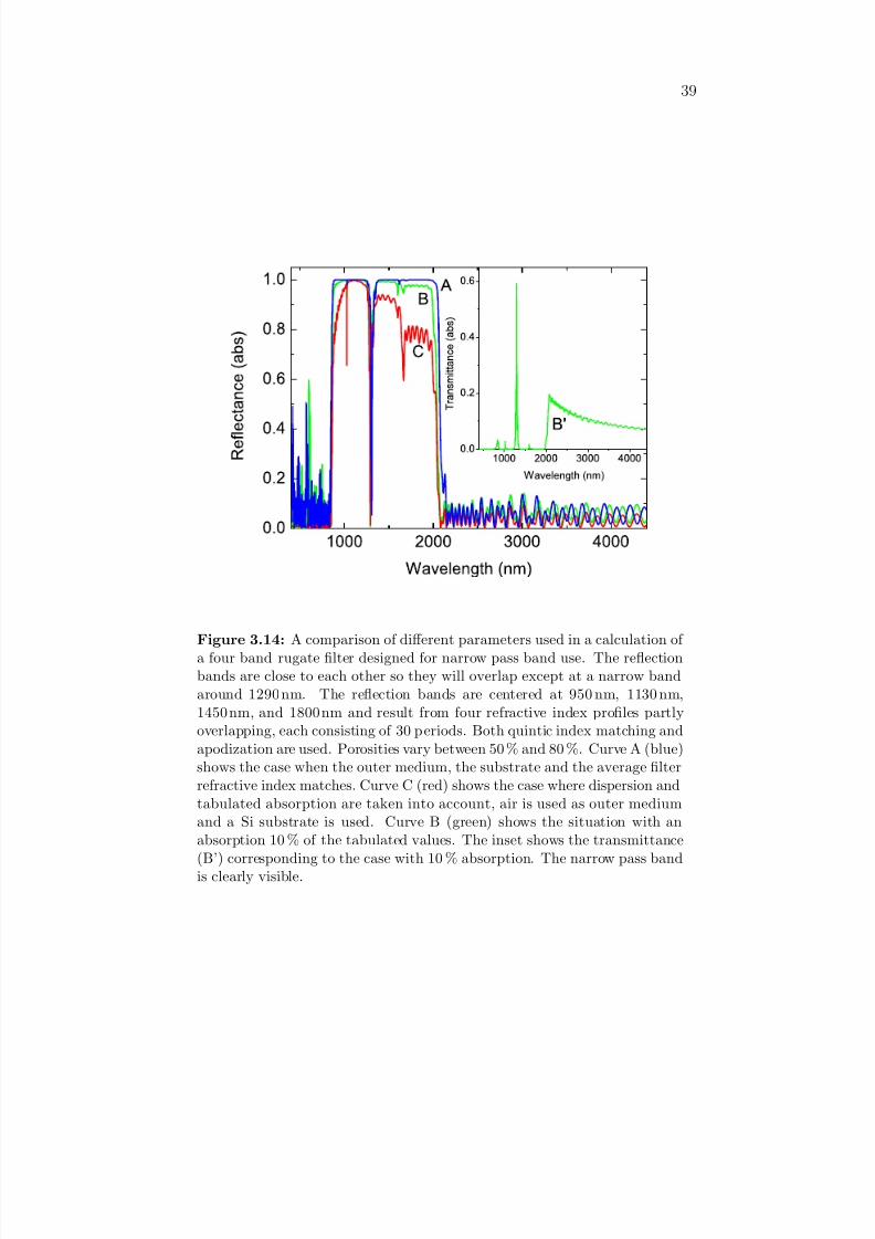
8/12/2019 Graded Optical Filters
http://slidepdf.com/reader/full/graded-optical-filters 49/164
39
Figure 3.14: A comparison of different parameters used in a calculation of a four band rugate filter designed for narrow pass band use. The reflectionbands are close to each other so they will overlap except at a narrow bandaround 1290 nm. The reflection bands are centered at 950 nm, 1130 nm,1450 nm, and 1800 nm and result from four refractive index profiles partlyoverlapping, each consisting of 30 periods. Both quintic index matching andapodization are used. Porosities vary between 50 % and 80 %. Curve A (blue)shows the case when the outer medium, the substrate and the average filterrefractive index matches. Curve C (red) shows the case where dispersion and
tabulated absorption are taken into account, air is used as outer mediumand a Si substrate is used. Curve B (green) shows the situation with anabsorption 10 % of the tabulated values. The inset shows the transmittance(B’) corresponding to the case with 10 % absorption. The narrow pass bandis clearly visible.

8/12/2019 Graded Optical Filters
http://slidepdf.com/reader/full/graded-optical-filters 50/164

8/12/2019 Graded Optical Filters
http://slidepdf.com/reader/full/graded-optical-filters 51/164
Chapter 4
In situ interferometry
experiment
For the efficient and successful fabrication of optical filters it is essential tohave good control of properties of the deposited material. The most im-portant properties are refractive index (also density/porosity, homogeneityand absorption) and interface roughness when discrete layers are deposited.When making optical elements in PS, especially filters, this translates tohaving a good (instantaneous) control of etch rate, porosity, roughness and,to some extent, microtopology as discussed in Sec. 3.1.
Etching of PS is a dynamical exercise. The parameters of the system changeduring etching which necessitates an in situ monitoring of the most impor-tant parameters so the changes may be counteracted, or enable a real-timefeedback to the etching process. The feedback method is often used to ob-tain optimum results in other conventional optical material systems [69].Often feedback in this situation is based on interference effects with mono-or poly-chromatic coherent light. Interference at single wavelengths and el-lipsometry give very good optical density/physical thickness resolution and,in the case of interference, is easily implemented in a deposition system.
In the PS fabrication setup already described, the sample is in contact
with a liquid electrolyte on one side. In this case it is easier to set up asystem where the optical probing is done from the opposite side than tohave the optics on the electrolyte side which may be closed off or corrosive.This presupposes a transparent sample which is obtained when using anIR laser with a wavelength longer than that corresponding to the siliconbandgap energy (λlaser 1130 nm). With this setup the IR laser beamwill encounter several interfaces, i.e. back side, PS-substrate, and front-side, with the resulting partially reflected beams phase shifted thus givingrise to interference in the measured reflected beam. Similar systems aredescribed by Steinsland et al. [80] for tetramethyl ammonium hydroxide
etching of silicon and by Thonissen et al. [81] and Gaburro et al. [82] forPS fabrication monitoring.
41

8/12/2019 Graded Optical Filters
http://slidepdf.com/reader/full/graded-optical-filters 52/164
42
The change in interference conditions during PS etching results in a signalcontaining information on relative interface movement and the differentrefractive indexes. By performing frequency analysis on this signal it is
possible to obtain several key parameters of a PS film during formation.The parameters depend on a few assumptions about the formation processand substrate material. Given the correctness of these assumptions, weobtain the refractive index and porosity profile of the PS film, and thetime dependent etch rate. From this we can calculate the refractive indexprofile of the film in air, average porosity and refractive index, PS-substrateinterface roughness, film thickness and instantaneous valence values duringformation.
Most of the work done with the setups presented here is described in Pa-pers I-III, which are included at the end of this chapter. These include
background theory, analysis, experimental setup, and some results. Somedetails not discussed in the papers are included in the following sections.
4.1 Setup
4.1.1 Usage
The goal of this work was to design an in situ measurement setup whichwould fit in with a standard etch cell as detailed in Sec. 2.4. As the analysisof the data obtained from the setup gives all the critical parameters withoutfurther processing of the sample, a quick, non-destructive measurement of the standard calibration parameters for constant current conditions is madepossible. These data, porosity and etch rate versus time and depth atconstant current, may be used for controlling the etch current to obtainlayers of constant porosity. The setups used are schematically shown inFig. 4.1. The main descriptions of the setups are given in Paper I and someof the concepts in the following discussion are defined in this paper.
In addition to the mentioned material properties, the evolution of interfaceroughness is also monitored by measuring the introduced partial incoherencein the reflected laser beam. The incoherence results in a decreasing signalintensity with increasing roughness. This is needed to better understandthe optical properties of the interfaces encountered in the multilayer PSoptical filters. By changing formation parameters, an optimal parameterrange may be found for filter fabrication with regards to interface roughness.This understanding is crucial for optimizing the quality of the PS opticalelements.
It is possible to test the calibration data by calculating the needed cur-rent profile for a constant porosity layer and measure the actual obtained
porosity with the setup in situ . An example of this will be given later.One challenge when using calibration data for a multilayer or inhomoge-

8/12/2019 Graded Optical Filters
http://slidepdf.com/reader/full/graded-optical-filters 53/164
43
neous refractive index structure, is that the conditions at the pore frontdepend on the ”history” of the etch. The conditions during multilayeretching is different from those present at the single layer calibration etch.
This effect may be seen by etching a single layer and changing the currentafter a certain time. Comparing the porosity obtained after the currentchange with porosities obtained by etching a layer at the same current asthis from the start, a shift in porosity is observed.
The measurement of the back side reflected signal will also give informa-tion on any change in refractive index or layer thickness of the porouslayer after the etch current is turned off. As the layer thickness is unlikelyto change, one must assume all change comes from the refractive index.This only applies if all else in the setup is constant, i.e. no thermal expan-sion/contraction or movement of the sample relative to the optics. A change
in refractive index after the electrochemical etch has stopped may be causedby a purely chemical etching of the porous structure. This chemical etchingof silicon by HF is very slow for the bulk material, but due to the largeinternal surface area of PS the relative time dependent change in Si volumemay be significant, thus will give a measurable change in refractive indexwith the in situ reflectance setup. However, there are several possible ex-planations to the change in refractive index after current is turned off, suchas relaxation of the structure due to decreasing temperature, electrolyte re-fractive index change due to diffusion, and oxidation of the structure in theelectrolyte. Similar measurements have been performed by Navarro-Urrios
et al. [83].It is possible to obtain a complete calibration curve, i.e. porosity versuscurrent density, by performing a current sweep during etching while mea-suring the interference signal. However, this will only be an approximationas it does not take into account the time dependent change in etching condi-tions. For many applications this approach may prove efficient and accurateenough. This technique is briefly discussed in Ref. [82].
One possible improvement of the current setup is to extend the data analysiscapabilities to real-time operation, hence facilitate the possibility of feed-back to the PS formation. With the knowledge of an approximate rangefor the starting porosity value, this technique could prove quite accurate.
4.1.2 Laser
Two laser systems were used. For the free space setup a 1310 nm wave-length laser diode (LD), LD1087, with drive electronics, LDP201, fromPower Technolgy was used. The diode was in a housing containing thecollimating optics. The output optical power was 8 mW and the beam di-ameter was about 2 mm with a divergence of about 10. By monitoring
the beam the quality of the measurement would increase by increasing thesignal-to-noise ratio. However, this was not necessary for obtaining satis-

8/12/2019 Graded Optical Filters
http://slidepdf.com/reader/full/graded-optical-filters 54/164
44
Figure 4.1: Schematic of the different etch setups. The setup denoted Ais based on free space beam transmission. The laser diode is denoted LD.The schematics of both setup A and B shows a cross-section of the etchbath. Setup B shows the wide beam optical fiber variant. MM denotes themultimode optical fiber and SM denotes single mode optical fiber. A coupleris shown; this splits the fiber and guides the reflected signal from the sampleto the detector. A graded index lens, as indicated, is used to collimate andcollect the light close to the sample. The third setup, C, shows a fiber variantwhere no collimating lens is used, but where the fiber is close enough to the
sample back side (< 500µm) to collect a significant amount of the lightreflected from the sample. This results in a probed area about the size of the fiber core cross section.
factory results.
For the optical fiber based setup a pigtailed laser system assembled byThorlabs was used. The diode used was of type ML976H11F from Mit-subishi, an InGaAsP, multiple quantum well, distributed feedback diodelaser. The output wavelength was 1550 nm with an optical power of 2 mW
when coupled to the single mode fiber.As the measurement of the interference effect in the reflected signal is de-pendent on a constant phase of the input beam, and also, for the calculationof roughness, a constant amplitude, a well regulated system is needed. Thediode lasers are sensitive to temperature fluctuations and temporal effects.To keep the output power and phase constant the diode needs to be stablein a specific laser mode. A small temperature change may introduce a mode jump which may give a change in phase and also a more noisy output asthere will be transient signals, both in the diode itself, and also in the regu-lation of the diode. Therefor careful regulation of temperature and output
power was needed. This was done using an ILX Lightwave TechnologiesLDC 3722 laser diode driver controlling the current by feedback from a

8/12/2019 Graded Optical Filters
http://slidepdf.com/reader/full/graded-optical-filters 55/164
45
monitoring diode in the laser package. The same driver regulated the diodetemperature with a thermo-electric element connected to the laser diodehousing with thermal paste. The diode lasing mode was very sensitive to
changes in temperature which resulted relatively often in unusable periodsin the measured data. This problem was improved by allowing the laserwarm up for a few hours before use.
The lasing in the diode is also very sensitive to back-reflected light fromthe pigtailed fiber. To minimize back-reflectance an optical isolator wasconnected to the fiber from the laser diode. By adding a second isolatorthe stability of the LD seemingly improved further. Because of a small but
significant time delay between an amplitude change in the LD and an am-plitude change in the signal reflected off the opposite end of the connectedfiber to the LD, instabilities in the regulation of the output-power may beintroduced. By introducing a light-”valve” so that the light is not reflectedback to the diode the problem of regulating the power may be reduced.Even though back-reflectance is very small with two isolators, there maystill be enough to introduce a slight oscillation in the output power whichmay explain one persisting artefact in the measurements. A long wave-length oscillation of equal or higher amplitude compared to the measuredinterference oscillation was present in all measurements. One possible causemay be instability in the laser, however, this was most likely ruled out bymonitoring the output signal by using a 2x2 coupler, with a monitoring de-tector and sample setup opposite the LD, and a reflectance signal detectoron the same side as the LD. This enabled the monitoring of the LD out-put concurrently with etching to see if the long wavelength oscillation waspresent in the output. The conclusion was that the oscillation is introducedby the etch setup ”arm” of the 2x2 coupler.
The standard design of a polarization insensitive optical isolator uses two
birefringent plates with a magnetic garnet crystal used as a Faraday rotatorsandwiched between. The beam from the fiber is collimated at input andoutput by lenses. The birefringent plates are wedge shaped such that theordinary and extraordinary rays at the input side are parallel but spatiallyseparated and the Faraday rotator rotates the polarization plane of eachbeam by 45, while the output birefringent plate maintain the spatial re-lationship between the two beams which are collected and coupled to theoutput fiber by a collimating lens. The returning beam will see a systemwhere the two birefringent plates do not keep the two beams parallel thusdissipating the beams in the cladding of the isolator. A typical isolation
effect of such a device will be over 40 dB for the optimized wavelength. Thedesign wavelength depends on the length of the Faraday rotator.
8/12/2019 Graded Optical Filters
http://slidepdf.com/reader/full/graded-optical-filters 56/164
46
4.1.3 Fiber
Due to availability, all connectors for the optical fibers were FC/PC. This
ensured a satisfactory coupling between fibers and relatively little interfaceback reflection. Possibly, by using FC/APC couplers the back reflectanceseen at the LD might be reduced somewhat, resulting in a more stable LDoutput.
Both multimode (MM) and single mode (SM) fiber were used in the setup.As the fiber pigtailed to the LD was SM, it would be optimal to onlyuse SM fibers due to back reflectance at connectors. However, it proveddifficult to couple the light reflected from the sample back into the SMfibers due to the small fiber core diameter and the small acceptance angleor numerical aperture. Because of the larger numerical aperture and core
diameter a MM fiber was used on the sample side of the setup. The SM fibercoupled to the LD was a standard SMF-28 type fiber with a core diameterof 8.3 µm, while the multimode fiber used had a 62.5 µm diameter core.Coupling between the two fiber types is not optimal. The core materialmay be different leading to Fresnel reflection losses, while the MM fiberwill have many available, unfilled modes which makes the fiber sensitive tomovement/bending etc. as the beam from the SM fiber may change modeas a response to external influences. To avoid these problems efforts weremade to keep all fibers as rigid and stable as possible by taping fibers andfastening all measurement equipment to the same metal frame. However, a
short length of the fiber from the 2x1 coupler to the etch setup was free asthe etch setup was inside a flow box with the rest of the equipment outside.One possible further remedy would be to fill all the modes of the MM fiberby scrambling the single model from the SM fiber, spreading the beam overseveral modes in the MM fiber.
The 2x1 coupler used was connected as shown in Fig. 4.1B. The split ratiobetween the two split fibers was 50/50.
4.1.4 Beam to sample coupling
How the ”probe” beam interacts with the sample is critical to the quality of the measurement. The three different setups used, free-space, wide-beam,and narrow-beam, all have different advantages which mainly depend onhow the beam couples to the sample.
In the case of the free-space setup, as shown in Fig. 4.1A, the ”probe”beam goes through air from the LD to the sample to the detector. Thebeam propagation direction is controlled by mirrors, and to simplify thesetup the beam is at an angle of about 12 to the sample normal. With thissetup there will be no back reflectance to the laser diode, hence, the laser
should be quite stable. However, by traveling through air, the beam maybe distorted by dust particles, changes in air density, moisture content and

8/12/2019 Graded Optical Filters
http://slidepdf.com/reader/full/graded-optical-filters 57/164
47
temperature, thus introducing noise in the measured signal. At the sametime the mechanical positioning of the LD, the detector and the samplemay drift slightly with time introducing amplitude shifts due to misalign-
ment. The beam is easily moved and changed in size. This may be used toprobe different areas of the sample, even scan the whole sample area duringetching by swiping the beam with a high speed beam movement system,e.g. bar-code scanner setup. By changing the beam size, the same setupmay probe roughness at different spatial scales, although the minimum ob-tainable beam diameter will be significantly larger than the effective beamdiameter obtained with the narrow beam fiber setup.
It is important for PS layer homogeneity, both in porosity and etch rate,that the electrical potential in the Si-sample is evenly distributed. Thisnecessitates a good, and optimally shaped, back contact, even for highly
doped Si-samples. See Sec. 2.4.1 for a discussion on this. However, as thecontact used is non-transparent aluminum a hole must be etched to letthe beam through. Depending on the size of this hole, the homogeneity of the PS film will be more or less affected. With the beam sizes obtainablewith the free-space setup this will always be a problem. An advantage of the free-space setup compared with the fiber based setups is that all theinterference comes from interactions in the sample, as opposed to interfer-ence between fiber end and sample back side. This assumes that the LDamplitude and phase is stable or oscillates very slowly compared to theinterference frequencies of interest.
In the wide-beam fiber setup the beam is transported to and from the sam-ple by optical fiber, thus avoiding many of the potential noise sources of thefree-space setup. However, as already noted, movement, bending or tem-perature gradients may also introduce noise in the fiber, but nonetheless thebeam in the fiber setup is relatively stable. As in the free-space setup, thereis a compromise between beam size and optimal back contact. However inthe fiber case the beam is more rigid. As can be seen in Fig. 4.2, to obtaina different beam a different graded index (GRIN) lens must be chosen andfitted.
Once a lens has been fitted, the Cu-plate must be leveled so that the beam
reflected off the sample will be coupled back into the lens. This need onlybe done once in a while as there is some reshaping of the materials usedin the sample holder when the sample is clamped down. This setup isvery compact and can be used as a standard addition to the etching of PS.There are a couple of challenges however. There is always the danger of leakage of electrolyte, so all parts of the etch setup should be HF resistant.For the setup used, this means a possible degradation of the the long termstability of the system as a non-HF-resistant GRIN lens was used as wellas an aluminum lens holder. There is also a possibility of interferenceeffects introduced in the signal from movement of the sample relative to the
lens, due to either temperature changes or bending of the sample duringetching [84]. This may be one explanation for the long period oscillation

8/12/2019 Graded Optical Filters
http://slidepdf.com/reader/full/graded-optical-filters 58/164
48
observed in the measured reflectance.
By avoiding the GRIN lens setup and only using the cut fiber end, theproblem of PS homogeneity is reduced as only a very narrow hole in the Alback contact is needed. In this setup a MM fiber is cut straight and placedas close to the sample as possible. In the used setup a small hole of about0.5 mm diameter was drilled in a Cu-contact plate in which the bare fiberend was positioned, see Fig. 4.3.
Figure 4.2: A zoom-in on the cou-
pling between fiber and sample forthe GRIN lens in situ setup. TheCu-plate with a center hole used asback contact is shown on top. TheGRIN lens is placed in an aluminumholder which is shown. There arescrews for adjusting the plane of theCu-plate in the top flange of the Allens holder so back coupling fromthe sample may be maximized. Thefiber is in contact with the end of
the GRIN lens for minimum back-reflectance.
Figure 4.3: The bare fiber end
setup uses wax to hold the fiber inplace. As can be seen, the outercladding of the fiber is stripped awayclose to the fiber end so the diame-ter of the hole in the Cu-contact maybe as small as possible. This resultsin as small as possible influence of the hole on the current distributionin the sample.
The fiber was pushed through as far as practical without leaving the endfree on the front side so it could break when the sample was positioned.This gave a distance between fiber end and sample of < 0.5 mm. On theother side of the Cu-plate the fiber was fastened with wax. This was stableenough and also made it easy to fix and recut the fiber in case of damage orwear to the end, e.g. by HF etching. This setup is able to measure the mostinteresting parameters without interfering with layer homogeneity, and as
the case with the wide beam fiber setup, can be an integral part of theetch setup. As the probed area of the sample in this setup has a diameter

8/12/2019 Graded Optical Filters
http://slidepdf.com/reader/full/graded-optical-filters 59/164
49
roughly the same as the core diameter, assuming relatively flat interfaces,the roughness measured may have spatial wavelengths smaller than theprobe diameter and thus will not be able to give a broad characterization
of the interface roughness of the sample. However, to get a good idea of the roughness, several different beam sizes must be used. The alignmentof this setup is very robust as the fiber has a wide acceptance angle, whichmeans the fiber end may still capture much of the interference even thoughit is somewhat tilted. To improve on back reflectance from the fiber end,the end may be cut at a small angle. However, the results were satisfactorywith a straight cut.
4.1.5 Other equipment
For both the free-space and fiber based setups, the sensor used was a NewFocus 2011 detector with built in amplification. It was based on a InGaAsPIN diode. This was connected to a multimeter, either a Keithley 199 DMMor a HP 34970A. This again was connected to a computer. The electrolytetemperature was measured with a Pt-based thermocouple for all calibrationmeasurements. Both temperature and signal was then logged by a LabViewprogram.
4.2 Data analysis
4.2.1 Chemical etching
In addition to etching at the pore tips there will also be some time dependentetching of the PS layer as discussed briefly in Sec. 4.1.1. This results in agradient in the porosity with depth opposite to the gradient observed bythe in situ measurements. The chemical etching results in an increasingporosity towards the surface which also will increase with time. The rate of this etching will change with time as the structure of the pores change due
to etching. A possible result of this is show in Fig. 4.4 where the back sidereflected signal is measured both during etching as well as after etch currentis turned off. The point where the etch current is turned off can be seenwhere the short period oscillation stops. A relatively slow oscillation is stillpresent indicating a continuing change in refractive index of the PS layer.In the upper right plot the oscillation present in the signal after etch currentis turned off is isolated and the slow variations are filtered out. As can beseen in the upper left plot of this figure, there is a very significant longperiod oscillation present throughout the measurement. This oscillation ismost likely caused by thermal gradients, slow movement of the fiber close
to the sample or bending of the sample as discussed in Sec. 4.1.4.It is possible that the end-of-etching oscillation is caused by these effects,
8/12/2019 Graded Optical Filters
http://slidepdf.com/reader/full/graded-optical-filters 60/164
50
Figure 4.4: Different aspects of a signal recorded during an in situ IR laserreflection measurement. The sample was etched at about 4.3 C in a 26 % HFelectrolyte at 30 mA/cm2 for 117 min. The etch setup used was the bare fiberend setup. The upper left figure shows the whole signal measured during theelectrochemical etching. The bottom figure shows the transition of the signalfrom short period oscillation due to electrochemical etching to a longer periodoscillation possibly due to chemical etching. The middle right figure showsthe long period oscillation high pass filtered so peaks are easier to quantify.The period between peaks is shown above the signal. The upper right figureshows the calculated change in porosity based on the signal period obtainedfrom the figure below.
however, the period and amplitude of the the most noticeable oscillationduring etching is quite different from the end-of-etch oscillation. Thereare other plausible explanations to the latter besides the external effectsand chemical etching. During etching the current through the electrolyteand the sample will drive up the temperature, possibly changing refractiveindexes of both the electrolyte and PS layer. When the etch current isturned off this change will relax back to the values at ambient temperature.
The refractive index of electrolyte may also change due to diffusion. Si-rich chemical species will diffuse out of the PS layer while HF will diffuse

8/12/2019 Graded Optical Filters
http://slidepdf.com/reader/full/graded-optical-filters 61/164
51
towards the pore front. Assuming that the end-of-etch oscillation is onlydue to chemical etching, the average porosity change in the layer is easilycalculated. The data shown in Fig. 4.4 is measured during formation of a
PS layer with an electrolyte containing 26 % HF at 30 mA/cm2
and at anaverage temperature of 4.3 C. The final etched thickness is 207.6 µm, thesample was etched for 117 min, while the average porosity of the layer is72.6 %. The optical thickness difference of the porous layer between twoadjacent oscillation peaks in the upper right plot of Fig. 4.4 corresponds tohalf the incident wavelength:
nPS,t1d − nPS,t2d = λ0/2 (4.1)
with nPS,t being the refractive index of the porous layer in the electrolyteat a time t and d is the layer thickness. This gives a change in the average
refractive index of the layer of about 0.0037 for each period of the oscillation.The resulting change in porosity is shown in the upper right plot in Fig. 4.4.
4.2.2 Effect of irregular sampling
A necessary condition for obtaining an optimal spectrogram, which willbe explained below, is that the sampling rate is constant throughout themeasurement. The FFT function presumes regular sampling, such that thesampling time of the data points of irregularly sampled data will be shifted
and thereby introduce errors and noise in the FFT spectrum. Some irreg-ularity is acceptable, and will at any rate most likely be introduced by thenumerical handling of the data. When the sampling period deviation fromthe constant/average sampling period is random, the noise introduced inthe FFT spectrum will be white noise, however, when there is a periodicityin the deviation this may introduce significant artifacts in the FFT spec-trum. Due to a discrepancy between the software set timestamp and theactual measurement time for a set of measurements, spurious signals wereintroduced. The periodic timestamp discrepancy probably had a sine-liketime dependence resulting in the spectrogram of Fig. 4.5b. The spectro-gram of Fig. 4.5a is obtained from the measurement of a sample fabricatedunder nearly the same conditions as for Fig. 4.5b, however, the timestampfor each data point was set by hardware and the sampling rate was nearlyconstant. The spurious partials in Fig. 4.5b are clearly seen, especiallyaround the partial marked 1.
4.2.3 Frequency analysis
Short time Fourier transform (STFT) is used for analysis of the obtainedsignal to give both temporal and frequency resolution. The details of the
analysis is discussed in Paper I. When selecting the parameters for theSTFT analysis, it is important to find an optimal balance giving the best

8/12/2019 Graded Optical Filters
http://slidepdf.com/reader/full/graded-optical-filters 62/164
52
Figure 4.5: A comparison between spectrograms obtained by analysis of measurements with data timestamped by a) the measurement hardware andby b) the measurement software. The small periodic error in the timestampsintroduced by the software results in spurious signals in the spectrogram asclearly seen in b).
result. This is critical for the choice of window, both which window functionand what length it should have. As the partials’ frequencies are likely tochange with time, increasing a window length will work towards broadeningthe observed peak, while at the same time the more periods of the partialsrepresented within the window, the better frequency resolution one shouldget. These effects oppose each other, hence for a partial with only a slightchange in frequency with time, represented in Fig. 4.6 as curve B, the effectof an increase in the number of oscillation periods overcomes the effect of the frequency change within the window. On the other hand, for curve A
in Fig. 4.6 the frequency change within the window is too large, resulting inthe broadening of the peak width with an increasing window length. Thedata in Fig. 4.6 shows the measured peak widths of the two main partialsof the in situ measured interference signal shown in the spectrogram of Fig.5 in Paper I varying the window width. Curve A corresponds to the partialmarked 1 while curve B corresponds to the partial marked 2. As can beseen in Fig. 4.6, for a decreasing window width under a certain thresholdvalue the peak width increases sharply. This is due to the lack of periodspresent within the window, hence the determination of a frequency becomesmore uncertain.
The choice of window function depends on which frequency peak featuresare most critical. Some window functions will give very sharp main peaks

8/12/2019 Graded Optical Filters
http://slidepdf.com/reader/full/graded-optical-filters 63/164
53
Figure 4.6: A comparisonof the effect of window func-tion length on the full widthat half maximum (FWHM) of the peaks corresponding to thetwo main partials of the spec-trogram in Fig. 5 in PaperI. The frequency of the par-tial corresponding to curve Bchanges little while the fre-quency of the partial corre-sponding to curve A changesmore resulting in change inFWHM as seen. The FWHM
is taken at 40 min.
but will also introduce a high level of noise, or sidebands, not containing anyinformation of interest. The shape of three different window functions areshown in Fig. 4.7a, these are the square window marked A, i.e. the result of not applying any particular window function, the Blackman window markedB and the Blackman-Harris window marked C. In the case of STFT analysis,the selected window is multiplied with the signal of a selected range beforethe FFT of the product is computed. By computing a FFT of the windowfunction itself one can see which effect a particular window function will
have on the result of the signal analysis. The FFT of the window functionsin Fig. 4.7a is shown in Fig. 4.7b. In general a window function giving avery narrow main peak will have high sidebands, while a window functionwith a wide main peak will have more subdued sidebands. For the presentanalysis, a balance between the two seems the best. We would like to beable to determine the frequency-trace of a partial as certain as possiblyrequiring sharp peaks, but, due to the tracing procedure, the height of thepeak ridge relative to the noise floor should be as large as possible. Asa compromise the Blackman window function was selected for the STFTanalysis.
4.2.4 Etch rate and porosity calculation
4.2.4.1 Measurement of the effect of limited HF diffusion
During constant current etch measurements with the in situ interferometrysetup the porosity and etch rate is observed to change with etched depth.This is thought to be caused by diffusion restrictions on electrolyte con-stituents to and from the pore tips changing the conditions of etching. Thiseffect will also be present when etching multilayers, and it is also likely that,
since this effect is caused by diffusion, the conditions change depending onthe pore structure of the layers already etched. Hence, after a given time

8/12/2019 Graded Optical Filters
http://slidepdf.com/reader/full/graded-optical-filters 64/164
54
Figure 4.7: Three normalized window functions are shown in a); a squarefunction (curve A), a Blackman function (curve B) and a Blackman-Harrisfunction (curve C). The resulting Fourier transform of these functions are
shown in b) in the corresponding colors.
the porosity at a given current density will be different in a layer etched atconstant current density compared to a layer etched at varying current den-sity. If one is to calibrate the etching of PS layers based on porosity profileand etch rate versus time data this change in etching conditions must betaken into account. If the variation in porosity is small through the layerthis effect may not need to be taken into account, however, if the variationis significant the difference between designed and obtained porosity profile
may be significant.An indication of the change in conditions at the pore front depending onthe ’etch history’ is shown in the following experiment. The reflection signalwas measured during the etching of a sample in a 26 % HF solution at 6 C.Etching was done first with 40 mA for 15 min then abruptly changed to20 mA for another 15 min. This change is clearly seen in the spectrogram inFig. 4.8 at about 13 min. Note that the time axes in the spectrograms areslightly offset as the time here denotes the starting point of the windowedsignal for each window position along the signal. Hence, the first powerspectrum plotted in the spectrogram, denoted t = 0, encompasses data from
t = 0 to t = window length. Figure 4.9 shows the calculated porosity of this sample. Note the large change in porosity within the first 15 min; from

8/12/2019 Graded Optical Filters
http://slidepdf.com/reader/full/graded-optical-filters 65/164
55
56.5 % to 64.5 %. The porosity changes abruptly as expected at t = 15 min.The second curve plotted after t = 15 min is the porosity obtained after15 min for a sample etched under the same conditions but with a constant
etch current of 20 mA from t = 0.The porosity of the dual current etched sample has shifted toward lowervalues compared to the constant current etched sample. This may be un-derstood as a consequence of a change in HF concentration assuming asimplistic view of the electrolyte chemistry at the pore front. This con-centration depends both on diffusion of HF to the pore front as well as onthe usage of HF depending on e.g. current density. The constant currentdensity etched sample has a certain porosity profile, resulting in a certaindiffusion of HF to the pore front, where the diffusion constant will changewith position through the layer. For the dual current density etched sample
the first half of the etching results in a different porosity profile than thatin the sample of constant current density etched after the first 15 min. Asthe current is higher in the first half, the porosity will be higher, hence ahigher diffusion of HF will result. From this one may assume that the HFconcentration at the pore front is higher for the dual etched sample after 15min of etching than for the constant etched sample after the same time. Inp-type silicon, it is well known [45] that a higher HF concentration, giventhe same current density, will result in a lower porosity. This gives a goodunderstanding of the results in Fig. 4.9.
4.2.4.2 Etch calibration
It is possible to use porosity and etch rate time dependence data to calibrateetching so that a known porosity with a known etch rate is obtained at anygiven time of continuous etching by changing the current density correctly.A constant time step has been used in the calculation of the needed currentdensity. The current density needed to obtain the desired porosity is foundby interpolating the porosity data at a given time for all the measuredcurrent densities and extracting the current density for the desired porosity.This is done for each time step until a given film thickness i reached. Theetched thickness for each time step based on the found current density isalso interpolated from the measured etch rate calibration data.
This procedure is based on the assumption that the etch condition at thepore front is a function of time and instantaneous etch current density only,independent of the earlier etch conditions. This is only an approximation,as exemplified by Fig. 4.9.
The data needed for this procedure are obtained by fabricating several PSlayers at constant current condition for different current densities. Thishas been done for two separate electrolyte conditions. A low temperature
etch in a 26 % HF solution was used for the results in Figs. 4.10 and 4.12.The etching was done in a refrigerator with an average temperature of 5 C,

8/12/2019 Graded Optical Filters
http://slidepdf.com/reader/full/graded-optical-filters 66/164
56
Figure 4.8: The spec-trogram of the reflectancemeasurements of a sam-ple etched with an abruptchange in etch current,the shift in the partialsfrequencies is clearly vis-ible at around 14 min.
Figure 4.9: The calculated porosity timeprofile of the sample used in Fig. 4.8 com-pared to the porosity calculated for a sampleetched from the start at the changed etch cur-rent. There is a notable shift in porosity be-tween the two profiles possibly indicating thatthe HF concentration changes with time dur-ing etching.
however, the temperature regulation was slow and the temperature in theelectrolyte varied ±3 C. The results shown in Figs. 4.11 and 4.13 were ob-tained during etching at room temperature with an electrolyte consisting of 15 % HF and 10 % of the ethanol replaced by glycerol. These results showthe generally accepted trends for PS formation in p-type Si; higher currentdensity leads to higher porosity and etch rate, and for a given current den-sity the porosity increases with a decreasing HF concentration. Also, clearlythe conditions for etching changes with time. This also follows what hasbeen reported earlier [85, 81, 82] in p-type PS. The trend is toward higher
porosities and lower etch rates with depth/time. Both observations fit witha picture of decreasing HF concentration with depth/time due to diffusionlimitations. Note that some exceptionally high porosity values are shownin Figs. 4.10 and 4.12. Porosity values above ≈90% are hard to obtainafter drying. Possible reasons for the shown porosity values are the use of the EMA effective medium formula which may give slightly shifted porosityvalues and that highly porous PS may still be mechanically intact duringetching. Highly porous PS is unstable mostly due to the capillary forceswhich occur during drying, resulting in breakage of the internal structure.
To test the calibration data, a PS layer was fabricated where the current had
been calculated beforehand to give a layer of uniform porosity throughoutthe depth. The back side reflection was measured during this fabrication

8/12/2019 Graded Optical Filters
http://slidepdf.com/reader/full/graded-optical-filters 67/164
57
Figure 4.10: The obtained poros-
ity time profiles for different currentdensities. The electrolyte used is26 % HF without glycerol and etch-ing is done at approximately 5 C.Porosities increase with current den-sity. Plotted are data for 1, 5, 10,15, 20, 30, 40, and 55 mA/cm2
Figure 4.11: The obtained poros-
ity time profiles for different currentdensities with an electrolyte consist-ing of 15% HF and 10% ethanolsubstituted with glycerol. Etch-ing is done at room temperature.Porosities increase with current den-sity. Plotted are data for 5, 10, 15,30, 50, and 70 mA/cm2.
so etch rate and porosity could be calculated. The porosity profile is shown
in Fig. 4.14. Due to the short window used in the STFT analysis thereare some irregularities which would be smoothed out with a longer win-dow. The etch duration was designed to give a layer of 10 µm thicknessand the current profile was designed to give a uniform 50 % porosity using26% HF at 5 C. The uniformity of the porosity in Fig. 4.14 shows thisis a feasible way of obtaining uniform layer porosity, however the porositymeasured is roughly 3 % (abs.) below the designed value and the thicknessobtained according to the reflectance measurement was 10.69 µm. The av-erage porosity was measured by gravimetry which gave a porosity of 52.0 %and a thickness of 9.56 µm. These discrepancies likely show the uncertaintyof the gravimetric method and the error introduced by the choice of aneffective medium approximation as discussed in Sec. 3.1.
4.2.4.3 Possibility of real-time monitoring
As seen in Fig. 4.4 and in the Papers I-III, the measured reflection signalhas a good signal-to-noise ratio. Assuming that the problem of the slowsignal oscillation is likely due to mechanical or thermal instabilities of thesetup/fiber, as discussed, may be resolved, the setup may well be used forreal-time monitoring of parameters or feedback control of etching parame-
ters. In the case of real time monitoring, the use of STFT is appropriate,however, prior knowledge of porosity and etch rate ranges will increase the

8/12/2019 Graded Optical Filters
http://slidepdf.com/reader/full/graded-optical-filters 68/164
58
Figure 4.12: Etch rates corre-
sponding to Fig. 4.10. Etch ratesincrease with current density.
Figure 4.13: Etch rates corre-
sponding to Fig. 4.11. Etch ratesincrease with current density.
Figure 4.14: The porositytime profile of a sample etchedwith a preset current pro-file calculated to give constantporosity with depth based on
the calibration data in Figs.4.10-4.13. The calculated un-certainty based on the FWHMof the peak in the spectrogramis plotted with dotted lines.
usability of such a system. This knowledge will ensure that the parame-ter space is limited such that the two main peaks in the STFT are foundquickly at onset of etching, see paper I for a description of the data analysis.In addition, optimization of the peak tracing algorithm is needed. In the
case of feedback operation, the use of STFT for frequency determination isonly appropriate if the current density used is constant with time or variesslowly, i.e. significant variations over much longer time than window func-tion length. In the case of multilayer etching, in which case the feedbackoperation would be most useful, the etching time for each layer will oftenbe too short for STFT based analysis. As seen in Fig. 4.15, which is fromthe etching of an infrared Bragg filter with layer thicknesses in the orderof a few 100 nm, each layer etching results in around one period, or less,of the main interference oscillation (main partial). With prior knowledgeof the system and an appropriate fitting algorithm, the information in this
signal may be used for feedback. Note that in Fig. 4.15 there are threeperiods; the high current layer with a high etch rate, the low current layer

8/12/2019 Graded Optical Filters
http://slidepdf.com/reader/full/graded-optical-filters 69/164
59
with a lower etch rate and a break period with no current. This is used toregenerate the electrolyte at the pore tips instead of adjusting the currentdensity to give the set porosity with changing electrolyte conditions.
Figure 4.15: The measuredin situ reflectance signal dur-ing etching of a multilayerstructure. One etch periodconsists of a high current layer,one low current layer and
one break period. These aremarked in the figure.

8/12/2019 Graded Optical Filters
http://slidepdf.com/reader/full/graded-optical-filters 70/164

8/12/2019 Graded Optical Filters
http://slidepdf.com/reader/full/graded-optical-filters 71/164
I
Paper I
S.E. Foss, P.Y.Y. Kan and T.G. FinstadSingle beam determination of porosity and etch rate
in situ during etching of porous silicon
J. Appl. Phys., 97, 114909 (2005)

8/12/2019 Graded Optical Filters
http://slidepdf.com/reader/full/graded-optical-filters 72/164

8/12/2019 Graded Optical Filters
http://slidepdf.com/reader/full/graded-optical-filters 73/164
Single beam determination of porosity and etch rate in situ during etchingof porous silicon
S. E. Foss, P. Y. Y. Kan, and T. G. Finstada
Department of Physics, University of Oslo, P.O. Box 1048 Blindern, N-0316 Oslo, Norway
Received 14 January 2005; accepted 1 April 2005; published online 31 May 2005
A laser reflection method has been developed and tested for analyzing the etching of porous silicon
PS films. It allows in situ measurement and analysis of the time dependency of the etch rate, the
thickness, the average porosity, the porosity profile, and the interface roughness. The interaction of
an infrared laser beam with a layered system consisting of a PS layer and a substrate during etching
results in interferences in the reflected beam which is analyzed by the short-time Fourier transform.
This method is used for analysis of samples prepared with etching solutions containing different
concentrations of HF and glycerol and at different current densities and temperatures. Variations in
the etch rate and porosity during etching are observed, which are important effects to account for
when optical elements in PS are made. The method enables feedback control of the etching so that
PS films with a well-controlled porosity are obtainable. By using different beam diameters it is
possible to probe interface roughness at different length scales. Obtained porosity, thickness, and
roughness values are in agreement with values measured with standard methods. © 2005 American Institute of Physics. DOI: 10.1063/1.1925762
I. INTRODUCTION
Porous silicon PS has been studied intensively for well
over a decade. The optical properties of PS have been of
particular interest. The application of PS for passive optical
devices came with the development of multilayer optical
Bragg reflectors by Vincent1
and Berger et al.2
in 1994.
Multilayer films in PS have shown great potential for a wide
range of applications. A variety of applications have lately
been fabricated, such as Si-based integrated optical circuits,3
chemical microsensors,4
and broadband laser mirrors.5
Most applications depend critically on the material prop-
erties. Many of the material properties of PS, such as the
optical, mechanical, and electrical ones, depend on the po-
rosity. The porosity depends on the process parameters.
Hence to achieve well-controlled properties a tight control of
process parameters is necessary. Ex situ characterization of
these properties is normally employed. Some characteriza-
tion techniques that are common are gravimetry for porosity
measurement, cross-section scanning electron microscopy
for thickness measurement, and profilometry for interface
roughness determination. These ex situ characterization tech-niques are all destructive and give no direct information of
the etch history or porosity gradients.
One critical aspect of using PS for many optical devices
is the inherent roughness at the different interfaces developed
during the etching process, especially the PS-substrate inter-
face. This roughness results in a nonoptimal optical quality
of the device. One mechanism of degradation, compared to
the ideal case, is scattering. The degradation in optical qual-
ity will be strong for short wavelengths as the scattering
power at a given roughness is inversely proportional to the
wavelength. The roughness is often described by a surface
height function of which a root-mean-square rms value is
obtained. Silicon has a very large absorption for wavelengths
below about 1.1 m, but freestanding transmission filters
and reflection filters on substrates are still possible for this
range. However, the low absorption and relatively smaller
scattering in the near-infrared spectral region above 1.1 m
make this range the best suited for optical filters based on
PS. Still, a tight control of the interface roughness is neces-
sary to obtain the optical quality needed for a given applica-
tion. Roughness in PS has been studied extensively by
Lérondel et al.6
as well as by Setzu et al.7
and Servidori
et al.8
A method for monitoring several parameters important
for optical element fabrication during etching of PS films
will be presented in this paper. The method is based on in-
terferometry where the oscillation frequency and amplitude
of a backside reflected monochromatic infrared IR laser
beam are measured in situ during PS formation. From this
single signal, and the following analysis, the PS film thick-
ness, the etch rate, the refractive index, the porosity, profile,
the average porosity, and the interface roughness may be
obtained. The calculations used for the analysis are based onAiry summation and Davies–Bennett theory.
9–11The analysis
of the measured signal is quite extensive and uses the fast
Fourier transform algorithm which easily facilitates an
implementation of an automated feedback system. The
method is quite robust and intuitive and may be adapted to
many different PS etching cells. The use of interferometry
techniques for monitoring parameters in situ during process-
ing of semiconductors has been reported before. Steinsland
et al.12
used IR laser backside reflection interferometry to
monitor the etch rate for tetramethyl ammonium hydroxide
TMAH etching of silicon, and the present work is an ex-
tension of that work. Thönissen et al.13
and Gaburro et al.14
applied a front side technique with a visible laser to monitoraElectronic mail: [email protected]
JOURNAL OF APPLIED PHYSICS 97, 114909 2005
0021-8979/2005/9711 /114909/11/$22.50 © 2005 American Institute of Physics97, 114909-1
Downloaded 01 Jun 2005 to 129.240.153.219. Redistribution subject to AIP license or copyright, see http://jap.aip.org/jap/copyright.jsp

8/12/2019 Graded Optical Filters
http://slidepdf.com/reader/full/graded-optical-filters 74/164
etch rate and porosity. The addition of the interface rough-
ness measurement to the refractive index and etch rate mea-
surements in the presented method results in an extended
characterization ability.
We will describe the experimental setup first in Sec. II.
There we also include the details of the samples where the
method has been used, supplementary characterization tech-
niques, and the determination of supplementary parameters
needed by the method. Then in Sec. III we outline the
method used and the theory behind it. In Sec. IV we present
some examples where the method has been used. These mea-
surements are briefly discussed in Sec. V.
II. EXPERIMENTAL DETAILS
A. Interferometric measurement setup
The preparation of PS films was done in a standard up-
right etch cell with a solid Cu back contact. Through a hole
cut out in the Cu back contact an IR diode laser was directed
at the sample and the reflected beam was detected with an
InGaAs detector. Three different measurement geometries
were used, with the main difference being the beam diam-
eter. Figure 1 shows a schematic of the different setups. Byusing different beam diameters it is possible to probe inter-
face roughness with different spatial wavelengths and also
obtain spatial averaging over probe areas of different sizes.
The latter implies a compromise between a large electrical
contact area on the sample backside, which is needed for
homogenous etching over the etch area, and large beam di-
ameter, needed for obtaining spatially averaged etch rate and
porosity data. Two of the setups were based on fiber optics
while the third was based on free-space optics. By using
optical fibers a compact setup was obtained and beam align-
ment and positioning were simple.
For both fiber setups, which are shown in Fig. 1 setups
B and C, the monochromatic, coherent light source usedwas a diode laser pigtailed to a single mode fiber with an
optical isolator. The wavelength was 1550 nm and the output
power was 2 mW. A 21 fused coupler was used to couple
the incident beam to the sample backside and the reflected
beam to the detector. The coupler used was based on a mul-
timode fiber. The beam collection in a multimode fiber are
easier than in a single mode fiber as both the core and ac-
ceptance angle are larger in the multimode fiber. For thenarrow beam fiber setup, Fig. 1 setup C, the bare multi-
mode fiber end was positioned close 500 m to the
sample backside through a hole in the Cu backplate. The
fiber core with a diameter of 62.5 m then collected light
from a probing area on the sample interfaces equal to the
fiber core area. This setup was used to measure roughness
with a short spatial wavelength. The other fiber setup, shown
in Fig. 1 setup B, used a collimating graded index lens to
give a collimated beam of 2-mm diameter. The beam was
oriented normal to the sample and the lens both collimated
the incident beam and collected the reflected beam and
coupled it back into the fiber. The free-space setup, shown in
Fig. 1 setup A, used a collimated beam from a laser diodewith a wavelength of 1310 nm and an output power of 8 mW.
The beam diameter was between 1 and 2 mm, however, it
could easily have been magnified to cover a larger area. The
beam was at an angle of 12° to the sample normal. The
sampling frequencies of the reflected light for all setups were
between 0.78 and 10 Hz.
B. Sample preparation
The wafers used for PS preparation were boron-doped
p-type Czochralski-grown 100-oriented, double side pol-
ished with a thickness of about 520 m and a resistivity of
0.01–0.02 cm. The electrochemical etching of the samples
was performed in an electrolyte made from 40% aqueous HF
diluted with ethanol and glycerol. The HF concentrations
used were 15%, 20%, and 26% while the glycerol-to-ethanol
ratio varied from 0% to 70%. Constant current densities ap-
plied were from 5 to 30 mA/cm2. Samples were etched up to
120 min at both room temperature RT and at a low tem-
perature LT of 5 °C.
C. Other experimental methods
Porosities were determined both by analysis of the re-
flected signal and by gravimetry. The layer thicknesses afteretching were determined by the reflected signal, by cross-
section observation in an optical microscope or by stylus
surface profilometry after stripping away the PS film in con-
centrated NaOH. The interferometrically measured rough-
ness values were compared to values obtained by white-light
interferometry measurements WYKO NT-2000 after strip-
ping away the PS.
Refractive indices of the different electrolytes used were
measured by the amount of parallel shift of a laser beam
transmitted through a holder made of Plexi-glass containing
the electrolyte while it was rotated and using Snell’s law.
Different concentrations of both HF and glycerol were used.
The inset in Fig. 2 shows a schematic of the experimentalsetup. The laser beam used had a wavelength of 1310 nm.
The refractive index was found to change little between 1310
FIG. 1. Color online Schematic of the different etch setups. The setup
denoted A is based on free-space beam transmission. The laser diode is
denoted LD. The schematics of both setups A and B show a cross section
of the etch bath. Setup B shows the wide beam optical-fiber variant. MM
denotes the multimode optical fiber and SM denotes single mode optical
fiber. A coupler is shown; this splits the fiber and guides the reflected signal
from the sample to the detector. A graded index lens, as indicated, is used to
collimate and collect the light close to the sample. The third setup C shows
a fiber variant where no collimating lens is used, but where the fiber is close
enough to the sample backside 500 m to collect a significant amount
of the light reflected from the sample. This results in a probed area about the
size of the fiber core cross section.
114909-2 Foss, Kan, and Finstad J. Appl. Phys. 97, 114909 2005
Downloaded 01 Jun 2005 to 129.240.153.219. Redistribution subject to AIP license or copyright, see http://jap.aip.org/jap/copyright.jsp

8/12/2019 Graded Optical Filters
http://slidepdf.com/reader/full/graded-optical-filters 75/164
and 1550 nm. A black-and-white charge-coupled device
CCD video camera SONY was used for measuring the
beam position.
III. THEORY AND METHOD
A. Determination of etch rate and porosity byinterferometry
We consider the situation sketched in Fig. 3 consisting of
three interfaces which all reflect and transmit a part of the
incident laser beam. The interaction of the beam with the
layers can be represented by individual rays, each having an
associated phase and amplitude. The signal to be detected
consists of the part of laser light being reflected into the
detector at the same side of the sample as the laser. This totalsignal will have contributions from many rays that interfere.
As the porous layer thickness increases as etching
progresses, the optical thickness of each layer changes and
the phase of each ray will vary. Thus the reflection signal
will vary in intensity with etching time. An example of an
experimental reflection intensity signal is shown in Fig. 4. If
we ignore absorption in the layers, the amplitude of each
partially reflected and transmitted ray is given by the product
of Fresnel coefficients from the encountered interfaces. As
will be shown later, the time varying signal can be decom-
posed into partials of specific frequencies and the frequencies
of these partials are those arising from the interference of ray
pairs. The rate of change of the phase difference between twodetected rays will give a partial with a specific instantaneous
frequency of oscillation. There are many rays contributing to
the detected signal which results in many possible partials of
different frequencies. However, most rays, and thus most
partials, will have very small amplitudes due to multiple re-
flections and transmissions. By extracting the appropriate
frequencies and their time dependence from the experimental
signal, it is possible to calculate the optical thickness and the
etch rate of each layer at any given time.
The schematic of the system in Fig. 3 shows the princi-
pal rays and partials used in the analysis. The phase differ-
ence between the ray transmitted at the air-substrate inter-
face, reflected once at the substrate-PS interface, andtransmitted back out ray II in Fig. 3 and the ray reflected at
the substrate ray I is given by
1t =2
0
nsub2 − sin2 d subt + 0 − d sub
, 1
while the interference frequency is
1t = 1t
t =
2
0
nsub2 − sin2 d d subt
dt . 2
Here nsub is the refractive index of the substrate, 0 is the
vacuum wavelength of the incident beam, is the incident
angle, while 0 and d sub are the phase changes on reflectionas the rays are reflected at the backside and at the PS-
substrate interface, respectively, these are assumed constant.
FIG. 2. Color online Measured refractive index of the electrolyte with
15% HF as a function of glycerol content. Glycerol content given in % of
total ethanol/glycerol content. The inset shows a schematic of the setup usedfor the measurement. The laser beam will be refracted twice disregarding
the holder walls, however, this is accounted for in the refractive index cal-
culation, into and out of the electrolyte, resulting in a measurable parallel
shift when the holder is rotated. This shift gives the refracted angle, which is
dependent on the difference in refractive index between electrolyte and air.
FIG. 3. Color online Ray trace through the sample during etching. Inter-ference between rays I and II is denoted as situation 1 and between I and III
as situation 2. Scattering of light due to a rough PS-substrate interface is
indicated.
FIG. 4. Color online Measured signal during etching of a sample with
20% HF and 10% glycerol at 20 mA. Oscillation caused by changing con-
ditions for interference due to a moving PS-substrate interface is evident.
The expanded view clearly shows that there are superposed partials.
114909-3 Foss, Kan, and Finstad J. Appl. Phys. 97, 114909 2005
Downloaded 01 Jun 2005 to 129.240.153.219. Redistribution subject to AIP license or copyright, see http://jap.aip.org/jap/copyright.jsp

8/12/2019 Graded Optical Filters
http://slidepdf.com/reader/full/graded-optical-filters 76/164
The substrate thickness, d subt , and the PS layer thickness,
d PSt , are time dependent. The etch rate is found by the time
derivative of either thicknesses. By defining the etch rate to
be positive when moving into the substrate and thereby
avoiding the absolute value in Eq. 2, it may be written as
r t = −d d subt
dt =
d d PSt
dt =0
2
1
nsub2 − sin2
1t . 3
If the interface does not move with a constant speed or the
porosity of the PS layer changes, the frequency will also
change. This information is present in the reflected signal.
Equation 2 contains no information of the porous layer.
The partial with this information is found when looking at
the interference between rays I and III in Fig. 3. The phase
difference here is given by
2t =1
0
2ODsubt + 2ODPSt + 0 − d surf , 4
where the constant phase change contribution is equivalent
to those occurring in Eq. 1. The substrate contribution to
the optical path difference between the two rays, OD subt , as
in Eq. 1, is given by
ODsub = nsub2 − sin2 d subt , 5
while the PS layer contribution, ODPSt , is slightly more
complex if the PS refractive index varies with depth. The PS
refractive index is modeled to have only depth dependence,
nPSl, where l is the depth or thickness of the layer, and not
an explicit time dependence as will be motivated in Sec. V.
The optical path difference caused by the PS layer is then
given by
ODPS = 0
d PSt
nPS2 l − sin2 d l. 6
Here the porous layer, d PSt thick, is divided into an infinite
number of sublayers of infinitesimal thickness dl. Each su-
blayer has a certain refractive index n PSl. The integral over
the optical path contribution of each sublayer then gives the
total optical path. Taking the time derivative of the phase
difference in Eq. 4 necessitates the use of the Leibniz’s rule
for differentiation of integrals15
to derivate Eq. 6, solving
for nPS then results in
nPSd PSt = nsub2 − sin2 −
0 2t
2r t 2
+ sin2 . 7
Using the measured refractive indeces for the different elec-
trolytes it is now possible to calculate the porosity profile
and average layer porosity as a function of PS layer depth.
Equations 3 and 7 together give the most important pa-
rameters of the PS etching process.
B. Interface roughness obtained by interferometry
To obtain information on the PS-substrate interfaceroughness, the interference between the ray reflected from
the substrate backside and the ray reflected from the
substrate-PS interface is of most interest. This corresponds to
situation 1 in Fig. 3. The intensity of the combined reflection
of these two rays, I ref , is given by
I ref = Asub2 + APS
2 + 2 Asub APScos sub − PS , 8
where Asub and APS are the amplitudes and sub and PS arethe phases of the rays reflected from the substrate backside
and the PS-substrate interface, respectively. The cosine com-
ponent of I ref gives the amplitude and frequency of the inter-
ference oscillation. The oscillation amplitude is given by the
cosine prefactor. Asub is constant while APS contains informa-
tion on the PS-substrate interface scattering, substrate ab-
sorption, and PS refractive index in the electrolyte,
APSt = t air-sub subt s R,sub-PSt r sub-PSt subt t sub-air . 9
Here t air-sub and t sub-air are the transmission amplitude coeffi-
cients, r sub-PSt the time-dependent reflection amplitude co-
efficient at the substrate-PS interface, s R,sub-PSt the time-dependent scattering factor as the roughness changes with
time, and subt the absorption factor which changes due to
a decrease in substrate thickness. The time dependence of the
reflection amplitude coefficient is due to the change in the PS
porosity with time.
Transmission and reflection amplitude coefficients, as
well as the absorption factor, are calculated using published
data for the complex refractive index of bulk Si. Normal
Fresnel relations are used for the transmission and reflection
coefficients, while the absorption factor is given by subt =exp−2 kzt / , where k is the imaginary part of the com-
plex refractive index and zt is the time-dependent substrate
thickness. The scattering factor value will be extracted fromthe interference data and is in the following assumed known.
This extraction is explained in Sec. III C below.
The Davies–Bennett theory9,10
attempts to describe the
local phase change in the reflected plane wave front intro-
duced by the height irregularities of the interface. These
phase changes result in a reduced intensity in the specular
direction as conditions for destructive interference will de-
velop between different parts of the wave front resulting in a
loss of coherence. The theory assumes a rms irregularity
height roughness value, , much smaller than the wave-
length of the incident light in the medium, , and that the
height function describing the roughness has a Gaussian dis-
tribution. In this case the Fresnel reflection coefficient for the
rough PS-substrate interface may be written as
Rsub = R0s R,sub-PS2 = R0 exp− 4 sub-PSnsub
0 cos sub
2 , 10
given the reflection coefficient for the perfectly flat surface,
R0. Here sub is the incident angle in the medium, n sub is the
refractive index of the incident medium, 0 the wavelength
in vacuum, and sub-PS the PS-substrate interface roughness.
Note that the spatial wavelength of the roughness does not
enter into this equation, so both long period for example,
striations and short period roughness as will have an equal
effect, depending only on sub-PS.To calculate the rms roughness of the front surface, a
scattering factor for transmission, sT ,sub-PS, must be calcu-
114909-4 Foss, Kan, and Finstad J. Appl. Phys. 97, 114909 2005
Downloaded 01 Jun 2005 to 129.240.153.219. Redistribution subject to AIP license or copyright, see http://jap.aip.org/jap/copyright.jsp

8/12/2019 Graded Optical Filters
http://slidepdf.com/reader/full/graded-optical-filters 77/164
lated based on the obtained sub-PS. The transmission coeffi-
cient at the PS-substrate interface has been shown by
Filiński11
to be
T sub = T 0sT ,sub-PS2
= T 0exp− 2 sub-PCnsubcos sub − nPScos PS0
2
,
11
for the same conditions as for the reflection coefficient in Eq.
10. Here T 0 is the transmission coefficient for a perfect
interface, while n PS is the refractive index of the PS and PS
is the angle in the PS layer. Then the reflected amplitude
from the front becomes
Afrontt = t air-sub sub2 t sT ,sub-PS
2 t t sub-PSt PS2 t s R,PS-front
t r PS-frontt t PS-subt t sub-air, 12
where most of the parameters are the same as in Eq. 9 withthe addition of a time-dependent transmission amplitude co-
efficient for the PS-substrate interface, t sub-PSt , a time-
dependent reflection amplitude coefficient for the PS-front
interface, r PS-frontt , and an absorption factor in the PS layer,
PSt , defined as for subt with k PS calculated by an
effective-medium theory using the complex refractive index
of bulk Si. The reflected amplitude is given by the same
calculations on the extracted amplitude of the partial in situ-
ation 2 of Fig. 3 as for A PS. The calculation of the scattering
factor, s R,PS-front, is the same as for s R,sub-PS and from this the
rms roughness value of the front surface is calculated.
C. Analysis
For the analysis of the reflected signal, the short-time
Fourier transform STFT was utilized to extract the different
frequency components. This gives both the frequency versus
time and the signal amplitude development. An example of a
reflection signal transformed with STFT is shown in the
spectrogram in Fig. 5a. The signal was measured during
etching of a sample in 26% HF at RT and 25 mA/cm2 with
the wide beam fiber setup. In the spectrogram several curves
are traced. These curves represent the observable and readily
understood partials of the signal and correspond to the situ-
ations schematically shown in Fig. 5b. In this figure, dif-
ferent ray trajectories and combinations are indicated whichwill give rise to the partials of the signal. The two main
partials in Fig. 5a are drawn as solid lines. These corre-
spond to, as labeled, situations 1 and 2 of Fig. 3 having
frequencies f and F , respectively. The dashed lines drawn in
Fig. 5a are calculated by the relation: n1 f ± n2F , where n1
and n2 are positive integers.
The analysis was done using the spectrogram and the
fast Fourier transform function in the software package
MATLAB.16
The STFT method uses a movable time win-
dow, where a Fourier transform is performed on the win-
dowed signal for each window position along the signal with
the assumption that signals have constant frequencies within
the window. Both the time resolution and the frequency reso-lution depend on the chosen window size, however, the de-
pendence follows a Heisenberg-type uncertainty relation; a
finer frequency resolution results in a coarser time resolution
and vice versa. With a narrow window, frequency peaks willbe relatively broad compared with larger windows. Different
window functions have different uses in signal processing. A
Blackman windowing function was used for this analysis as
it gave the best compromise between frequency resolution
and sidelobe suppression. To obtain the required detail of the
traced curves, consecutive windows overlapped by 95%.
Two window sizes were used when analyzing the data; 6 and
12 min of data. This resulted in comparable spectrograms
and peak widths between different samples and it was a good
compromise between time resolution and peak width.
In the case that the constant frequency assumption does
not hold and the frequency of a signal changes within a win-
dow, the frequency peak will increasingly broaden with win-dow length, hence there will be an optimum window length
giving the narrowest peaks. As changing signal frequencies
FIG. 5. Color online a An example of a spectrogram. The peaks drawn
by the solid lines are the two dominant partials, corresponding to situations
1 and 2 in Fig. 3, as denoted on the spectrogram. The change of frequency
with time is evident. The dashed lines are the readily understandable higher-
order partials, calculated by n1 f ± n2F , where n1 and n2 are positive integers
and f and F are the frequencies of curves 1 and 2, respectively. Most higher-
order partials are not detectable. The sample was etched at RT for 120 min
with 25 mA/cm2 and 26% HF. The length of the Blackman windowing
function used for the STFT analysis was 6 min 3600 samples and the
overlap between consecutive windows was 95%. b The corresponding ray
traces of the different higher-order reflections shown in the spectrogram.
114909-5 Foss, Kan, and Finstad J. Appl. Phys. 97, 114909 2005
Downloaded 01 Jun 2005 to 129.240.153.219. Redistribution subject to AIP license or copyright, see http://jap.aip.org/jap/copyright.jsp

8/12/2019 Graded Optical Filters
http://slidepdf.com/reader/full/graded-optical-filters 78/164
are assumed in this analysis, the signal peak at a given time
will be an average over signal frequencies within the window
and the true position of the peak at that time is not certain
unless the frequency shift is linear with time. However, the
rate of change of the frequency of a signal may change dur-
ing a measurement which results in a change in the optimumwindow length. In the present analysis two window lengths
were used for all samples as a compromise between peak
definition and time resolution. For simplicity, it is assumed
that the true peak position is unknown but within the full
width at half maximum of the calculated peak. Calculations
of porosity, etch rate, and thickness include this uncertainty.
This assumption is likely to overestimate the actual uncer-
tainty of the peak position as the Fourier transforms of con-
secutive time windows will correlate. Uncertainty introduced
by the experiment is much smaller than the uncertainty in-
troduced by the analysis and the model used. Experimental
uncertainty includes uncertainty in the incident angle, refrac-
tive index of the substrate, flatness of the interfaces, mea-surement sampling rate, and the laser wavelength. There is
an additional uncertainty in the calculation of the porosity as
this value depends on the effective-medium model used.
To find the etch rate, porosity profile, and interface
roughness, it is only necessary to track the two strongest
partials in the spectrogram and obtain their history. The ray
combinations shown in Fig. 3, giving rise to situations 1 and
2, will have the fewest possible interface interactions of the
possible oscillation producing combinations in the total re-
flected signal. The amplitude of each ray will decrease with
the number of interface interactions due to both scattering/
coherence loss and partial reflection/transmission. Based onthe presented system model, the two curves with the largest
amplitudes in the obtained spectrogram will correspond to
the two situations denoted in Fig. 3. Of the two main curves,
the curve with the lowest frequency will always correspond
to situation 2 as the total optical thickness for ray III changes
slower than that for ray II of Fig. 3. Equation 2 gives the
frequency of the interference between rays I and II. The
curve corresponding to this situation curve 1 will not al-
ways have the largest amplitude compared to curve 2 when
the ray is reflected off a rough substrate-PS interface even
though it has gone through the least number of interface
interactions. The reason for this is that the amplitude of the
reflected ray is affected more by interface roughness than thetransmitted amplitude.
11The traces of these two curves are
performed assuming small variations in the peak frequencies
from one window to another. This assumption is well
founded based on the measurements performed. Since each
time slice in the spectrogram is a frequency versus power
spectrum, the starting points of the two strongest partials are
found from the spectrum for zero time t = 0. This procedure
is well suited for real-time implementation with an expecta-
tion of the first frequency value as input in the tracking rou-
tine. With this a feedback control could be realized.
The procedure for calculating the scattering factor of
Eqs. 9–12 starts by smoothing the extracted partials am-
plitude. This is done by fitting the amplitude to a doubleexponential. The function was chosen because it showed a
good fit to most of the obtained amplitudes. Smoothing is
done to avoid the amplitude fluctuations present in a partial
around the position where the frequency of another partial
momentarily crosses. Crossing partials are present in the
spectrogram in Fig. 5a as can be seen for both main curves
at about 88 min. The fitted amplitude is then scaled so that
the extrapolated value at t =0 corresponds to the theoreticalamplitude with zero scattering. The scaling is necessary be-
cause the measured data are not normalized to unit reflec-
tance. Because of the windowing of the measured signal the
amplitude values are averaged over the time span the win-
dow covers, hence the STFT amplitude values calculated for
the lowest time value are correct for the partial at a time
around the middle of the first window. The exact position
depends on the shape of the amplitude change within the
window, but is for all calculations presented here assumed to
be at the middle of the window. This necessitates an extrapo-
lation of amplitude to t =0. The fitted and scaled amplitude
functions correspond to the cosine prefactor of Eq. 8 from
which APSt and Afrontt can be calculated.
D. Electrolyte refractive index
To get the right porosity value of the PS layer, knowl-
edge of the refractive index of the etchant is necessary as the
value obtained from frequency analysis is the refractive in-
dex of the PS layer when it is immersed in the etchant. An
effective-medium model must be used to approximate the
porosity, which both accounts for the refractive index of the
silicon substrate and the etchant. The Bruggeman approxima-
tion theory was chosen as this is most often used for PS in
the literature.17
The refractive index of glycerol in the visible
is 1.466 while for ethanol it is 1.365 and for water it is 1.350,hence glycerol will influence the etchant refractive index sig-
nificantly. Refractive index values for solutions with concen-
trations different from those measured are extrapolated from
the measurements assuming a linear dependency between re-
fractive index and both HF and glycerol concentration. Some
data with error bars are shown in Fig. 2. For the analysis
presented in Secs. III A–III C the electrolyte refractive index
is assumed constant and independent on time and thickness
of the PS layer. This assumption could be violated if the
electrolyte composition changes close to the pore tips due to,
e.g., diffusion limitations on the HF concentration as well as
buildup of Si-rich chemical species. However, the use of the
assumption seems well justified based on a comparisonbetween porosities obtained by interferometry and by
gravimetry.
IV. EXPERIMENTAL RESULTS
Using the method presented above some results from
analyzing measured reflection signals will be presented in
the following. The parameters obtained were the etch rate,
PS layer thickness, average porosity versus time and etched
thickness, porosity versus depth porosity profile, and inter-
face roughness. Firstly, the effect of the beam size on the
measured amplitude will be shown. Following this is an ex-
ample of the change in porosity and etch rate with time.Further, a comparison between average porosities obtained
by interferometry and by gravimetry will be given. The ef-
114909-6 Foss, Kan, and Finstad J. Appl. Phys. 97, 114909 2005
Downloaded 01 Jun 2005 to 129.240.153.219. Redistribution subject to AIP license or copyright, see http://jap.aip.org/jap/copyright.jsp

8/12/2019 Graded Optical Filters
http://slidepdf.com/reader/full/graded-optical-filters 79/164
fect on average porosity of different HF and glycerol con-
centrations will be shown next. After this some PS-substrate
interface roughness measurement results will be given as
well as the time dependence of the valence of a few samples.
Some of the measurements used to test this method have
been reported earlier.18
Those measurements were all done
with the free-space optics setup.
The difference in using the wide beam and narrow beamsetups can be seen in Fig. 6. Here two experimental runs are
compared. They use the same parameters; 26% HF,
15 mA/cm2 at RT, but were performed in different setups.
The traced amplitude of the partial corresponding to curve 1
in Fig. 5a is plotted for both experimental runs. The ampli-
tudes have been scaled so that their starting values are iden-
tical. For both cases the general trends in the amplitudes are
the same; there is a decrease in the beginning due to rapidly
increasing roughness. This is overtaken by an increase in
amplitude due to less absorption in the substrate as the PS
film grows. There is a clear difference in the relative impor-
tance of these effects, loss due to scattering/coherence loss
and loss due to absorption, between the two experimentalruns using different beam sizes. In the case using the narrow
beam setup the initial decrease is much less, indicating a
significantly smaller measured roughness within the beam
spot than for the wide beam case, hence the relative effect of
the decreased absorption is greater. This is a strong indica-
tion that there are different spatial wavelengths of roughness
of importance at different spot sizes. In most of the following
measurements the wide beam free-space or fiber-optic setup
has been used as the signal-to-noise ratio is better.
All the p+ samples etched at constant current conditions
in this study have shown an increase in porosity with longer
etching time. This increase is the result of the increasing
porosity with depth which is exemplified in Fig. 7 where theporosity profile of one of the samples is calculated and plot-
ted. To be able to compare the porosity measured by gravim-
etry with the interferometrically obtained data, the average
porosity as a function of time is also calculated. The average
porosity values are plotted with the porosity profile in Fig. 7.
The etch rate also changes with time. This is plotted in Fig. 7
as well. Note that in these examples the largest change for
both porosity and etch rate is at the beginning of the etching.
For all three parameters upper and lower limits are shown.
These curves correspond to the full width at half maximum
values of the traced peaks discussed earlier in determining
the true peak position, hence gives an upper limit on the
uncertainty in the calculation. The sample data shown in Fig.
7 are the result of an analysis of the spectrogram in Fig. 5a.
The sampling frequency for this sample was 10 Hz and the
window length used in the analysis was 6 min 3600
samples. The sample was etched at RT with 26% HF and
25 mA/cm2 and the wide beam fiber-optic setup was used.
The average porosity data value for five different
samples was measured by the interferometry method de-
scribed. The samples were etched in an electrolyte contain-
ing 26% HF and ethanol at different current densities. The
average porosity value at three different times for all five
FIG. 6. The oscillation amplitudes of the signals corresponding to situation
1 in Fig. 3 and curve 1 in Fig. 5a for measurements prepared with different
setups. The solid curve represents a measurement made with the narrow
beam fiber-optic setup. The amplitude decreases slightly in the beginning as
a result of a slight increase of PS-substrate interface roughness, while later
the amplitude increases because the effect of a thinning substrate, i.e., less
absorption, overtakes the amplitude loss due to scattering. For the measure-
ment made with the wide beam fiber-optic setup ---- the effect from thethinning substrate is not large enough to overcome the decrease in amplitude
due to more scattering at the interface as the beam area is large enough to
encompass striations. Etching is done at room temperature with 26% HF and
15 mA/cm2.
FIG. 7. An example of a porosity profile solid line in depth upper hori-
zontal axis /time lower horizontal axis and the accompanying etch rate
change. The time development of the average porosity is also indicated
dashed line. Data are from the same sample as in Fig. 5a. The dotted
lines are an indication of uncertainty based on the peak width of the signal
line in the spectrogram.
FIG. 8. Color online The average porosity as a function of current density
given at three different times. Samples are etched with 15% HF. denotes
15-min etching, denotes 25-min etching, and denotes 45-min etching.
114909-7 Foss, Kan, and Finstad J. Appl. Phys. 97, 114909 2005
Downloaded 01 Jun 2005 to 129.240.153.219. Redistribution subject to AIP license or copyright, see http://jap.aip.org/jap/copyright.jsp

8/12/2019 Graded Optical Filters
http://slidepdf.com/reader/full/graded-optical-filters 80/164
samples is plotted against current density in Fig. 8. It is seen
that the porosity increases smoothly with current density, as
expected. In addition the average porosity increases with
time for all the measurement series, as is also exemplified inFig. 7. The increase of porosity with time has been reported
earlier for p+ Si,13
so this behavior is expected. The final
average porosities obtained by interferometry for a different
set of measurements are shown in Table I where the values
can be compared with those measured gravimetrically. It can
be seen that the porosity values agree well within the errors
given. It should also be noted that the interferometrically
obtained porosity values increase more consistently with cur-
rent density than the gravimetrical measurements.
The absolute change in average porosity with time seems
to be identical for different concentrations of HF, about 10%
over 50 min, this implies a substantially larger difference in
porosity between PS layer surface and bottom, as can be seenin the porosity profile data in Fig. 7. A comparison of the
average porosities of PS etched with different HF concentra-
tions is shown in Fig. 9. The uncertainty for all the porosity
calculations is about ±3%. The error bars are not shown for
clarity. Figure 10 shows the average porosity obtained after
etching as a function of glycerol concentration for samples
etched in 15% and 26% HF solutions at the same current
density. This plot clearly indicates a varying effect of glyc-
erol on porosity dependent on the HF concentration.
Roughness estimates were also made based on the
method discussed. The plot shown in Fig. 11 is representa-
tive of the samples prepared in this experiment. Here the rms
roughnesses of two samples are plotted against layer thick-
ness during etching. The samples are etched with identicalparameters except for a difference in glycerol content. The
sample with 10% glycerol shows a power-law dependence of
roughness on thickness, however, with values substantially
smaller than for the sample etched without glycerol. The
latter sample shows a saturation occurring at around 10 m
after a similar power-law dependence. A saturation of rough-
ness has been reported before in the case of p and p − PS.6
In
Table II the interferometrically obtained maximum rough-
ness values of several samples are compared with white-light
interferometry WLI roughness values obtained from the
PS-substrate interface after stripping of the PS layer with
NaOH. The data shown are from samples measured with the
wide beam fiber setup. A WLI spot size similar to the spot
size obtained with the interferometry setup was used. As
there was some curvature over the whole etched interface as
well as fluctuations in thickness with spatial wavelengths
longer than the spot diameter the rms roughnesses when
measured over the whole etched area for these samples were
significantly larger.
From the local porosity data and the etch rate data as
determined by interferometry and the measured anodic cur-
rent, it is possible to calculate the valence of the reaction,
TABLE I. Comparison between average gravimetrically measured and interferometrically measured porosities
%. The fit is quite good, values obtained by interferometry even give a more consistent change in porosity
with change in current density. The electrolyte used contains only HF and ethanol. Etching was done at RT.
Average porosity %after etching in 26% HF
Average porosity %after etching in 15% HF
Current density
mA/cm2 Gravimetry Inte rferometry Gravimetry Interferometry
5 36 32 69 65
10 43 40 65 66
15 38 ¯ 66 71
20 48 46 80 79
30 53 53 83 ¯
FIG. 9. Color online Comparison of the evolution of average porosities
with time for different HF concentrations. All three measurements are madeon samples etched with 20 mA/cm2 and no glycerol at RT. As expected,
porosities decrease with increasing HF concentration. The time evolution is
quite similar for all samples.
FIG. 10. The effect of the glycerol content in the electrolyte on average
porosity for different concentrations of HF. The points from samples etchedin 15% HF are marked with and 26% are marked with . The glycerol
ratio is compared to the total ethanol/glycerol content. There is a clear
difference between the 15% and 26% HF cases.
114909-8 Foss, Kan, and Finstad J. Appl. Phys. 97, 114909 2005
Downloaded 01 Jun 2005 to 129.240.153.219. Redistribution subject to AIP license or copyright, see http://jap.aip.org/jap/copyright.jsp

8/12/2019 Graded Optical Filters
http://slidepdf.com/reader/full/graded-optical-filters 81/164
i.e., the charge required to remove one silicon atom from the
substrate. It is assumed that the etching only occurs at the
pore tips,14,19
= j
Nerp, 13
where is the valence, j the current density, N the numbers
of silicon atoms per unit volume, e the elementary charge, r
the etch rate, and p the porosity at the interface. Figure 12
shows the valence determined this way as a function of timefor several samples etched at different conditions. Tempera-
ture, current density, HF concentration, and glycerol content
have all been varied to see the effect on the valence.
V. DISCUSSION
The presented interferometric method has been tested.
From the etch rate data, PS layer thicknesses may be calcu-
lated which corresponds well with stylus surface-profile
measurements. The obtained refractive index at the PS-
substrate interface gives a film porosity profile from which
the average layer porosity may be calculated. This corre-
sponds well with gravimetrically obtained porosities. The ob-
tained rms roughness also corresponds well with other mea-
surements. Thus, we consider the obtained results for good.
The present setup is slightly different than setups presented
before12–14
and the analysis is more extensive.
In the present setup as well as in Ref. 12, the beam is
transmitted through the sample using an IR laser beam for
which Si is transparent, hence there will be no free-carrier
generation in the sample. When preparing PS it is of great
importance for reproducibility to control the access of charge
carriers, specifically holes, to the etched surface. By using an
IR laser, the beam intensity may be quite high without influ-
encing the etching. This gives a good signal-to-noise ratio.
The use of an IR beam also facilitates the measurement of
thick layers in comparison with a beam in the visible rangewhich will be absorbed within the first few microns. On the
other hand a shorter wavelength will improve the resolution
of thickness and etch rate. The transmission setup may easily
be adapted to a liquid back contact etch cell. By directing the
beam from the backside, disturbances from hydrogen
bubbles in the beam path through the electrolyte are avoided.
To obtain both etch rate and porosity either one or two beams
may be applied. In the two-beam case, the beams must have
different wavelengths or different incident angles. Only the
top layer needs to be probed in this case, hence a simple
reflection signal is obtained, however, for this to happen
there must be enough absorption or a highly scattering inter-
face to avoid reflection from the back surface.14
In the one-beam case the beam must be able to probe more layers and
this results in a more complex reflection signal also making
it more complicated to analyze. However, having only one
beam simplifies the setup. Further, by using fiber optics, the
footprint of the setup is minimized making it more mobile
and space efficient and making alignment easier.
When preparing multilayer structures for optical filter
applications in PS, thicknesses less than 20 m are normally
used to minimize absorption, for filters used in the visible
range even thinner filters are made. It is clear that the varia-
tion in porosity within the first few microns of etching will
be detrimental to the properties of the optical filters if not
taken into account in the design.20 The results shown in Fig.7 suggest that the greatest change in porosity with depth
occurs within the first 20–30 m. By changing current den-
TABLE II. Comparison of measured roughness rms values by interferom-
etry with the wide beam fiber setup and values obtained with white-light
interferometry WLI on a 2-mm-diameter circular area at the center of each
sample after stripping of PS. LT is low temperature 5 °C and RT is room
temperature. Note that thicknesses will not be the same for different
samples.
Etch condition
Small area WLI
rms nm
Reflectance
measurement
rms nm
26% HF, 15 mA/cm2, RT, 100 min 157 157
15% HF, 15 mA/cm2, RT, 120 min 173 170
26% HF, 15 mA/cm
2
, RT, 120 min 168 16926% HF, 15 mA/cm2, LT, 120 min 155 153
26% HF, 30 mA/cm2, LT, 120 min 187 186
FIG. 11. Roughness nm rms obtained from calculations using the reflec-
tion signal amplitude data for two samples etched with 15% HF at RT with
different glycerol content. 10% glycerol gives the lowest roughness in the
case of 15% HF of all concentrations tested. The roughness saturation of the0% glycerol data has been reported earlier Ref. 6 for lower-doped p -type
PS.
FIG. 12. Valence calculated based on etch rate and porosity as a function of
time for samples etched with several variations in etching parameters. It is
evident that the different parameters have a large effect.
114909-9 Foss, Kan, and Finstad J. Appl. Phys. 97, 114909 2005
Downloaded 01 Jun 2005 to 129.240.153.219. Redistribution subject to AIP license or copyright, see http://jap.aip.org/jap/copyright.jsp

8/12/2019 Graded Optical Filters
http://slidepdf.com/reader/full/graded-optical-filters 82/164
sity during etching according to this knowledge it is possible
to obtain PS layers of uniform porosity through the layer.13
An alternative is to use etch stops to regenerate the electro-
lyte to its original condition and thus avoid a change in etch-
ing condition at the pore tip.20
As shown with the presented method, a porosity gradientis a common characteristic of the fabrication technique used
for PS preparation today, i.e., constant current conditions and
a closed, constant electrolyte volume. However, both posi-
tive and negative gradients have been reported in the
literature.8,14,21
The gradient seems to depend on the sample
doping and formation conditions. The etch rate will typically
also change with time, as shown in Fig. 7. Both of these
effects are routinely overlooked, with a few notable excep-
tions where very good filters have been fabricated.22,23
When
not accounting for these effects there will be noticeable dis-
crepancies between the designed filter characteristics and the
experimentally obtained, especially for thick filters, e.g., IR
filters. The observation of a porosity gradient has usuallybeen performed by extensive modeling on data obtained by
variable angle spectroscopic ellipsometry24–26
or synchrotron
x-ray reflectivity8
as a more direct measurement of the gra-
dient has proven difficult, e.g., by electron microscopy tech-
niques. The models used for ellipsometry or x-ray reflectivity
data are not always transparent and the necessary fitting
could give only local minima and not necessarily the best
values. The method presented in this paper is based on a
fairly simple model, in addition, the measurements are done
in situ resulting in the formation history being part of the
model input. Thus, one need only to find the porosity of the
last infinitesimal homogenous layer at any given time to havethe complete porosity profile. However, to obtain the best
possible porosity profile, a combination of the in situ inter-
ferometric method with an ex situ ellipsometry measurement
would be necessary.
The choice of p+ Si for etching PS for optical applica-
tions is based on the large obtainable porosity range and the
reported comparably low interface roughness. There are,
however, a few challenges with p+ PS. Because of the high
dopant concentration, absorption will be slightly higher com-
pared to p and p− PS. The high concentration also gives rise
to larger spatial fluctuations in the dopant concentration, of-
ten referred to as striations, hence spatially varying etch rates
and porosities are obtained. These fluctuations are often ob-served as concentric circles in the PS, as the refractive index
is affected during etching, or as ridges on the interface sur-
face after PS stripping.6
The radial distance between ridges is
most often in the order of 250 m. By using a probing area
smaller than this the ridges will spread little of the light,
hence this roughness will be filtered out and roughness
caused by other effects will be measured, hence the need for
beams of different diameters.
In the literature13,21
two different causes for a depth de-
pendence of the refractive index of the porous layer are
given: i etching of the porous structure not considered to be
caused by electrochemical etching, i.e., chemical etching,
which leads to a time-dependent porosity increase in alreadyetched parts of the PS film, and ii an increase or decrease in
the porosity at the etch front with time with otherwise con-
stant conditions caused by changing local conditions for
etching with time. This change in local conditions at the etch
front is thought to be caused by diffusion limitations on the
local HF concentration. In p+ PS, chemical etching has been
reported to be very small for the electrolytes used here,
hence this effect has been neglected in the present analysis.Using the same interferometric setup as in Ref. 14,
Navarro-Urrios et al.27
have shown the effect of chemical
etching on the detected interference signal; an oscillation is
still present even after the etch current has been turned off,
possibly indicating a change in the refractive index, and
hence the porosity, of the PS layer. A slow oscillation after
turning off the etch current has also been observed in the
measurements discussed in the present paper, although this
may have other causes than chemical etching, such as ther-
mal effects. A rough estimate of the possible chemical etch-
ing effect on the refractive index of a typical sample etch
conditions: RT, 26% HF, 15 mA/ cm2, 100-min etching,
150 m thick using one period of the oscillation in the mea-sured signal after the current is turned off gives an average
change in the refractive index for the whole thickness of
about 0.07/h immediately after etching. This translates to a
porosity change of roughly 2.5% /h. This estimate shows
that chemical etching in this case is indeed a small effect and
gives a maximum uncertainty in the porosity profile values
of the order of the uncertainties already discussed.
In the model considered in Sec. III, the etching is con-
sidered to occur only at the pore tip. This is an approxima-
tion to the actual situation where several factors will deter-
mine the reaction distribution over the surface of the pore.19
Note that this assumption will influence the porosity profile
determination, but not that of the average porosity.
There are several methods available to perform joint
time-frequency analysis of a signal besides STFT; these are
mainly the wavelet transform and the Wigner–Ville distribu-
tion. The Wigner–Ville distribution was not used because of
problems with cross terms. The measured signal obtained
through the discussed setup shows relatively low-frequency
oscillations, hence the requirement of stationarity within
each window of the STFT is close to satisfied. It is of im-
portance to have the best compromise between time and fre-
quency resolution in the frequency range of interest. As the
wavelet transform gives an increasing frequency resolution
and decreasing time resolution for a decreasing signal fre-quency the choice of resolution is limited. With the STFT the
resolution is the same for all frequencies and it may be set to
optimize the resolution and uncertainty of the calculated pa-
rameters. Further the STFT is easily implemented and more
intuitive than the wavelet transform.
VI. CONCLUSION AND SUMMARY
The method presented here shows the possibility of
monitoring multiple process parameters simultaneously dur-
ing the formation of a porous silicon layer with a fairly
simple setup. The extracted values using the method are in
good agreement with those obtained using other ex situ ordestructive methods. The validity of the method is further
justified by giving the same trends as reported in the litera-
114909-10 Foss, Kan, and Finstad J. Appl. Phys. 97, 114909 2005
Downloaded 01 Jun 2005 to 129.240.153.219. Redistribution subject to AIP license or copyright, see http://jap.aip.org/jap/copyright.jsp

8/12/2019 Graded Optical Filters
http://slidepdf.com/reader/full/graded-optical-filters 83/164
ture for porosity versus depth. Analysis of the mean porosity
and the etch rate evolution during etching caused by a gra-
dient in the porosity with depth was discussed as well as the
effect of different HF concentrations has on these param-
eters. The effect of glycerol in the electrolyte was also
shown, looking at both porosity change and roughness evo-lution. The spectrogram calculation can be done in real time
and this has potential for feedback control of the etching
process using the measured parameters in the feedback loop.
ACKNOWLEDGMENTS
This work is supported by the Research Council of Nor-
way. The authors are grateful for help by Chetna Schukla and
Erik S. Marstein during the initial experiments.
1G. Vincent, Appl. Phys. Lett. 64, 2367 1994.
2M. Berger et al., J. Phys. D 27, 1333 1994.
3M. Ha, J. Kim, S. Yeo, and Y. Kwon, IEEE Photonics Technol. Lett. 16,
1519 2004.4V. Mulloni and L. Pavesi, Appl. Phys. Lett. 76, 2523 2000.
5W. Zheng, P. Reece, B. Sun, and M. Gal, Appl. Phys. Lett. 84, 3519
2004.6G. Lérondel, R. Romestain, and S. Barret, J. Appl. Phys. 81, 6171 1997.
7S. Setzu, G. Lérondel, and R. Romestain, J. Appl. Phys. 84, 3129 1998.
8M. Servidori et al., Solid State Commun. 118, 85 2001.
9H. Davies, Proc. Inst. Electr. Eng. 101, 209 1954.
10H. Bennett and J. Porteus, J. Opt. Soc. Am. 51, 123 1961.
11I. Filiński, Phys. Status Solidi B 49, 577 1972.
12E. Steinsland, T. Finstad, and A. Hanneborg, J. Electrochem. Soc. 146,
3890 1999.13
M. Thönissen et al., Thin Solid Films 297, 92 1997.14Z. Gaburro, C. Oton, P. Bettotti, L. Dal Negro, G. Prakash, M. Cazzanelli,
and L. Pavesi, J. Electrochem. Soc. 150, C381 2003.15
K. Rottmann, Matematische Formelsammlung, 4th ed. Bibliographisches
Institut Wissenschaftsverlag, Mannheim, Germany, 1991.16
MATLAB R13 The MathWorks, Inc., Natic, MA, 2002.17
D. Aspnes and J. Theeten, Phys. Rev. B 20, 3292 1979.18
P. Y. Y. Kan, S. E. Foss, and T. G. Finstad, Phys. Status Solidi A in press.19
X. Zhang, J. Electrochem. Soc. 151, C69 2004.20
S. Billat, M. Thönissen, R. Arens-Fischer, M. Berger, M. Krüger, and H.
Lüth, Thin Solid Films 297, 22 1997.21
M. Thönissen, S. Billat, M. Krüger, H. Lüth, M. Berger, U. Frotscher, and
U. Rossow, J. Appl. Phys. 80, 2990 1996.22
P. Reece, G. Lérondel, W. Zheng, and M. Gal, Appl. Phys. Lett. 81, 4895
2002.23
M. Ghulinyan, C. Oton, Z. Gaburro, P. Bettotti, and L. Pavesi, Appl. Phys.
Lett. 82
, 1550 2003.24L. Pettersson, L. Hultman, and H. Arwin, Appl. Opt. 37, 4130 1998.
25S. Zangooie, R. Jansson, and H. Arwin, J. Mater. Res. 14, 4167 1999.
26M. Fried and L. Redei, Thin Solid Films 364, 64 2000.
27D. Navarro-Urrios, C. Pérez-Padrón, E. Lorenzo, N. Capuj, Z. Gaburro, C.
Oton, and L. Pavesi, Proc. SPIE 5118, 109 2003.
114909-11 Foss, Kan, and Finstad J. Appl. Phys. 97, 114909 2005
Downloaded 01 Jun 2005 to 129.240.153.219. Redistribution subject to AIP license or copyright, see http://jap.aip.org/jap/copyright.jsp

8/12/2019 Graded Optical Filters
http://slidepdf.com/reader/full/graded-optical-filters 84/164

8/12/2019 Graded Optical Filters
http://slidepdf.com/reader/full/graded-optical-filters 85/164
IIPaper II
P.Y.Y. Kan, S.E. Foss and T.G. FinstadThe effect of etching with glycerol, and the interfer-
ometric measurements on the interface roughness
of porous silicon
Phys. Stat. Sol. (a), 202, 8, 1533 (2005)

8/12/2019 Graded Optical Filters
http://slidepdf.com/reader/full/graded-optical-filters 86/164

8/12/2019 Graded Optical Filters
http://slidepdf.com/reader/full/graded-optical-filters 87/164
phys. stat. sol. (a) 202, No. 8, 1533– 1538 (2005) / DOI 10.1002/pssa.200461173
© 2005 WILEY-VCH Verlag GmbH & Co. KGaA, Weinheim
Original
Paper
The effect of etching with glycerol, and the interferometricmeasurements on the interface roughness of porous silicon
P. Y. Y. Kan*, S. E. Foss, and T. G. Finstad
Department of Physics, University of Oslo, P.O. Box 1048 Blindern, 0316 Oslo, Norway
Received 23 July 2004, revised 21 September 2004, accepted 27 January 2005
Published online 8 June 2005
PACS 68.35.Ct, 68.55.Jk, 81.05.Rm, 81.40.Tv, 82.45.Vp
We have carried out interferometric measurements of interface roughness in-situ during electrochemical
etching of p-type porous silicon (PS) at room temperature. We found that at a certain porosity (~70%) andwith an electrolyte where a low fraction (10%) of the ethanol was replaced with glycerol, there was a sig-
nificant decrease of the interface roughness. However, a higher content of glycerol (>10%) increased the
surface roughness. We have varied the current density in the electrolytic cell and the HF concentration of
the electrolyte. We also found that the porosity of the PS varied only slightly when glycerol at various
concentrations was used. This investigation shows that an interferometric technique could be a useful tool
for measuring the etch rate and the interface roughness of the PS.
© 2005 WILEY-VCH Verlag GmbH & Co. KGaA, Weinheim
1 Introduction
Porous silicon (PS) can be easily used to fabricate into optical structures such as waveguides [1], opticalfilters [2, 3] or luminescent microcavities [4] because its refractive index can be easily modulated.
Chemical and biological sensors based on modulation of the optical properties of PS have also been
made [5]. The interface roughness between PS and silicon (Si) plays a very important role in PS optical
devices. Light transmission can undergo severe losses through scattering if the interfaces are not smooth.
There are many parameters that can affect the roughness of the PS. For example, the type and resistivity
of the Si substrate, the composition of the electrolyte, i.e. the ratio between HF, H2O and ethanol (EtOH),
the current density ( J ) and the temperature of the electrolyte. The latter two parameters have been stud-
ied recently [6, 7] where it was shown that lowering the temperature decreases the interface roughness of
PS which was attributed to the increase of viscosity. Glycerol will also increase the viscosity and was
reported to reduce the roughness of PS-substrate interface [7].
2 Experimental methods and results
In this study we used glycerol as a partial replacement for ethanol in an electrolyte with ratios from
10–70%. The electrolyte consisted of HF:(EtOH:glycerol). The effect of different current densities and
HF concentrations was also measured. The etching solution was prepared from 40% HF diluted with
EtOH in a ratio depending on the desired percentage of HF. The PS-substrate interface movement and
roughness were measured in-situ during etching by a simple interferometric technique with an infrared
diode laser beam incident from the dry backside of the sample. Experiments were conducted at room
* Corresponding author: e-mail: [email protected]

8/12/2019 Graded Optical Filters
http://slidepdf.com/reader/full/graded-optical-filters 88/164
1534 P. Y. Y. Kan et al.: The effect of etching with glycerol, and the interferometric measurements
© 2005 WILEY-VCH Verlag GmbH & Co. KGaA, Weinheim
temperature with p+-type Si wafers. The average porosity for each experiment was determined by the
gravimetric method. The obtained average thickness was typically around 50 µm. The starting material
was p+-type Cz (100) silicon, double-side polished with a thickness of 520 µm. The resistivity was 0.01–
0.02 Ω cm.
The experimental setup for in-situ interferometric measurement during etching is shown schematically
in Fig. 1. A two-electrode Teflon cell was placed on a stand equipped with two inclined mirrors that
guided the infrared (IR) laser beam (λ = 1.31 µm, maximum power is 8 mW, spot size is 1–2 mm in
diameter). The copper electrode had the centre opened so that the laser light could reach the Si wafer and
interference could be produced from the bulk Si and the PS layer while etching. A constant current den-
sity of 5 to 30 mA/cm2, supplied from a Keithley 2400 current source, was applied for 1 hour while the
interference signal was sampled in each experimental run. An example of the measured interference
signal is shown in Fig. 2. The signal amplitude clearly falls off with time which is an indication of in-
creasing roughness.
For easy parameterization we have defined ‘roughness’ here as a percentage which is calculated, asillustrated in Fig. 3a, from the difference between the modulation start amplitude, A
max, and that at time t ,
A(t ):
Roughness = ( Amax
– A(t ))/ Amax
· 100 . (1)
0 10 20 30 40 50 60
15%HF 10mA 30% glycerol
I n t e n s i t y ( a . u
)
Time (min)
(b)(c)
(a)
54 56 58 60
t
I n t e n s i t y ( a . u
)
Time (min)
0 2 4 6
I n t e n s i t y ( a . u
)
Time (min)
IR Laserdetector
Teflon
Pt-
+
HF:EtOH
Si waferCopper
mirror
Fig. 1 (online colour at: www.pss-a.com) Schematic diagram of
interferometric measurement on the interface roughness of PS. The
wavelength of the infrared laser is 1.31 µm.
Fig. 2 Enlarged views for 60 minute
measurement of IR laser reflection from the
backside of the sample during etching: (a)
original interference pattern; (b) zoomed
fragment of first 6 minutes; (c) last 6 min-
utes.

8/12/2019 Graded Optical Filters
http://slidepdf.com/reader/full/graded-optical-filters 89/164
phys. stat. sol. (a) 202, No. 8 (2005) / www.pss-a.com 1535
© 2005 WILEY-VCH Verlag GmbH & Co. KGaA, Weinheim
Original
Paper
Time
Amax A(t )
PS
3
1
laser
Si2
Figure 3b illustrates the reflection from various interfaces in a PS sample. Interference between the par-
tially reflected IR beams (1, 2, 3) can easily be measured. The amplitude of the signal will be dependent
on the roughness of the interfaces. Beams (2) and (3) may get weaker as etching proceeds and as the
reflected light undergoes diffuse scattering which gives weaker interference signals. Thus the modulation
amplitude decreases (narrower width) with time (see Fig. 2a). The waveform shape and periodicity canbe analyzed by Fourier decomposition to monitor etching rate and porosity as a function of time, which
will be presented in future works. The roughness parameter as here defined is influenced by uneven etch
rate over the whole area of the laser beam, fluctuations in the effective dielectric constant of the PS layer
due to bubbles and by scattering of the beam. Both interfaces will contribute. A good review of common
ways of quantizing roughness can be found in Ref. [8].
A plot of the roughness against the PS thickness is shown in Fig. 4. There was not much difference
in the roughness for the 26% HF sample (Fig. 4a) as the glycerol percentage was varied. However,
for the sample in Fig. 4b (15% HF, porosity of 70%), there was a large difference in the roughness be-
tween samples with 0% and 10% glycerol. The sample with a 10% glycerol replacement of ethanol indi-
cates a relatively smooth interface, whereas the one without glycerol shows a very high roughness per-
centage.
The 30 and 70% glycerol samples also show a smoother surface than the 0% glycerol sample(Fig. 4b), but these are comparatively rougher than the 10% case. This implies that glycerol is an effec-
tive agent for smoothing the interface roughness. However, the results also indicate that a high glycerol
content (>10%) would not be as effective as the 10% sample. This could be due to the fact that the con-
tent of ethanol also plays an important role in the etching solution, which can be speculated is related to
0 10 20 30 40 50 600
20
40
60
80
100
Time (min)605040302010
porosity ~45%
26%HF
10mA/cm2
R o u g h n e s s ( % )
Thickness (um)
0% glycerol
10% "
30% "
50% "
70% "
0 10 20 30 40 50 600
20
40
60
80
100
Time (min)80604020
porosity ~70%
15%HF
10mA/cm2
R o u g h n e
s s
( % )
Thickness (um)
0% glycerol
10% "30% "
70% "
(a) (b)
Fig. 4 Graphs showing the calculated roughness change in samples etched with different electrolytes. (a) An elec-
trolyte with 26% HF is used with changing glycerol content, and (b) an electrolyte with 15% HF is used. In the 15%
case it is clear that 10% glycerol gives the lowest roughness. In the 26% HF case the effect is not so large.
Fig. 3 (a) Diagram showing a method for
determining the PS roughness. Amax
is the
maximum amplitude, A(t ) is the amplitude attime t . (b) Reflection from various interfaces
in a PS sample.
a) b)

8/12/2019 Graded Optical Filters
http://slidepdf.com/reader/full/graded-optical-filters 90/164
1536 P. Y. Y. Kan et al.: The effect of etching with glycerol, and the interferometric measurements
© 2005 WILEY-VCH Verlag GmbH & Co. KGaA, Weinheim
0 10 20 30 40 50 60
20mA
15mA
12mA
10mA
5mA
15%HF 10%glycerol
I n t e n s i t y ( a . u
)
Time (min)
(b)
0 10 20 30 40 50 60
12mA
15mA
20mA
10mA
5mA
15%HF 0% glycerol
I n t e n s i t y ( a . u
)
Time (min)
(a)
Fig. 5
Interferometric results from the15% HF samples at different current densities, 5–20 mA/cm2 for 60 minutes.
Plot (a) with 0% and (b) with 10% glycerol.
the dependency of bubble formation on viscosity and surface energy during the etching, where ethanol
has a favourable effect.
Figure 5 shows the interferometric results from the 15% HF (porosity 70%) samples, one with 10%
glycerol and one without, and the current density varied from 5 to 20 mA/cm2. By observing the modu-
lation amplitude of the interference graphs for the 0% glycerol samples (Fig. 5a), it is evident that
the roughness has an irregular trend. This means that the roughness as measured here varies for nomi-
nally identical conditions. However, the trend seems to be steady for the 10% glycerol samples. For all
samples investigated we always produce low roughness with that percentage of glycerol. Detailed analy-
sis indicates that the 10% samples did indeed smooth this irregular trend, as is shown in Fig. 6 (15%
HF).Other samples with different HF concentration (13–26% HF, porosity 85–50%) are also presented in
Fig. 6 which all indicate a steady trend from the 10% glycerol samples. Largely varying roughness for
nominally identical experimental conditions can only be observed from the samples with the higher po-
rosity and without glycerol replacement (13% and 15% HF samples). This indicates that the roughness of
the high porosity samples, at least in respect to the current measurement method, is critically dependent
0 10 200
40
80
10 20 30
0% glycerol
10% "
26%HF
10 20 30
J (mA/cm2)
20%HF
10 20 30
15%HF13%HF
r o u g h n e s s
Fig. 6 (online colour at: www.pss-a.com) A plot of roughness against current density at 13% to 26% HF which
correspond to the porosity of 85 to 50%, respectively. The 15% HF sample with 0% glycerol has two attempts of
measurements.
8/12/2019 Graded Optical Filters
http://slidepdf.com/reader/full/graded-optical-filters 91/164
phys. stat. sol. (a) 202, No. 8 (2005) / www.pss-a.com 1537
© 2005 WILEY-VCH Verlag GmbH & Co. KGaA, Weinheim
Original
Paper
0 10 20 30 40 50 60 700
20
40
60
80
100
0.01 ohm·cm
10mA/cm2
P o r o s i t y ( % )
% glycerol
13% HF
15% "26% "
(b)
0 5 10 15 20 25 30
0
20
40
60
80
100
0.01 ohm-cm
solid line - 0%glyceroldot line - 10%glycerol
P o r o s i t y
( % )
J (mA/cm2)
13% HF15% "
26% "
(a)
Fig. 7
A plot of porosity against current density (a), and against glycerol percentage (b), at 13% to 26% HF. Dif-ferences between 0% and 10% glycerol are also shown in (a).
on the etching parameters. The addition of glycerol seems to yield conditions which are in a part of the
parameter space which is much less sensitive to either the etching conditions or parameters of the rough-
ness measurements. It has been suggested [7] that the smoothness of interfaces of PS and Si can be un-
derstood in terms of diffusion limited asperity smoothing. The nature of the roughness on several length
scales should be investigated further. Lérondel et al. [8] has made measurements of the evolution of
interfaces which suggest a saturation. The present experiments were not designed to test this.
From an optical application point of view a key issue is whether the same porosity and the same opti-
cal properties can be achieved with and without glycerol. To ensure that the 0% and 10% glycerol re-
placement is comparable, their porosities should be in a narrow range. We thus carried out a porosityanalysis on each sample and the results are shown in Fig. 7a. Interestingly, they only show a little differ-
ence, the porosities between samples with 0% and 10% glycerol varied only slightly, indicating that the
results were comparable.
Figure 7b shows the porosity of the samples made with different percentage of glycerol replaced with
ethanol, measured at three different concentrations of HF. The lower percentage of HF (13% HF) has a
higher porosity (85%), whereas the higher percentage of HF (26% HF) has a lower porosity (45%). The
porosity change with varying glycerol percentage at a particular HF concentration does not vary too
much, but seems to be in an acceptable range. For the 15% HF sample, the porosity was only varied from
60 to 70% as the glycerol content changed from 0 to 50%.
3 Conclusion
The simplicity and the usefulness of the IR laser in-situ interferometric measurement of etch rate and
roughness have been demonstrated, and the effect of glycerol on PS interface roughness have been
measured. These measurements show that glycerol is effective for smoothing the interface roughness of
the PS for a small range of glycerol concentrations and for certain HF concentrations, while glycerol
replacement has little or no effect when higher concentrations of glycerol, up to 70% replacement of
ethanol, are used. The 10% glycerol replacement in 15% HF solution seems to be the most effective in
smoothing the interface compared to no glycerol.
Acknowledgements We thank Chetna Shukla and Erik Marstein for help during the initial stages. This work is
supported by the Norwegian Research Council.

8/12/2019 Graded Optical Filters
http://slidepdf.com/reader/full/graded-optical-filters 92/164
1538 P. Y. Y. Kan et al.: The effect of etching with glycerol, and the interferometric measurements
© 2005 WILEY-VCH Verlag GmbH & Co. KGaA, Weinheim
References
[1] A. Loni, L. T. Canham, M. G. Berger, R. Arens-Fischer, H. Munder et al., Thin Solid Films 276, 143 (1996).[2] G. Lammel, S. Schweizer, and Ph. Renaud, Sens. Actuators A 92, 52 (2001).
[3] L. Pavesi, C. Mazzoleni, A. Tredicucci, and V. Pellegrini, Appl. Phys. Lett. 67, 3280 (1995).
[4] M. Cazzanelli, C. Vinegoni, and L. Pavesi J. Appl. Phys. 85, 1760 (1999).
[5] V. S.-Y. Lin, K. Motesharei, K.-P. S. Dancil, M. J. Sailor, and M. R. Ghadiri,
Science 278, 840 (1997).
[6] S. Setzu, G. Lérondel, and R. Romestain, J. Appl. Phys. 84, 3129 (1998).
[7] M. Servidori, C. Ferrero, S. Lequien, S. Milita, A. Parisini et al., Solid State Commun. 118, 85 (2001).
[8] G. Lérondel, R. Romestain, and S. Barret, J. Appl. Phys. 81, 6171 (1997).

8/12/2019 Graded Optical Filters
http://slidepdf.com/reader/full/graded-optical-filters 93/164
III
Paper III
S.E. Foss, P.Y.Y. Kan and T.G. FinstadIn situ porous silicon interface roughness character-
ization by laser interferometry
Accepted for publication in the Proceedings of the3rd Pits and Pores symposium, 206th Meeting,ECS, Hawaii, 2004

8/12/2019 Graded Optical Filters
http://slidepdf.com/reader/full/graded-optical-filters 94/164

8/12/2019 Graded Optical Filters
http://slidepdf.com/reader/full/graded-optical-filters 95/164
IN SITU POROUS SILICON INTERFACE ROUGHNESS
CHARACTERIZATION BY LASER INTERFEROMETRY
S.E. Foss, P.Y.Y. Kan and T.G. FinstadDepartment of Physics, University of Oslo
P.O.Box 1048 Blindern, N-0316 Oslo, Norway
ABSTRACT
In situ laser reflection measurements during etching of porous silicon
(PS) films are used for analyzing the time dependency of interfaceroughness, etch rate and porosity. The interaction of an IR laser beam
with a time changing layered system of PS and substrate results in an
interference effect in the reflected beam which is analyzed by Short-Time
Fourier Transform (STFT). Using this method, the effect on roughness of
different temperatures, different etchant solutions and different formationcurrent densities is measured. Calculated roughness values are in
agreement with other methods.
INTRODUCTION
After nearly 15 years of intense research into the optical properties of porous silicon
(PS) there is still a great activity today. This activity has increasingly been focused on the
application of PS in devices such as Si-based integrated optical circuits (IOC) (1) and
chemical microsensors (2). The first application of PS for passive optical devices camewith the development of multilayer optical Bragg reflectors by Vincent (3) and Berger et
al. (4).
One critical and limiting aspect of using PS for many optical devices is the inherent
roughness at interfaces developed during the etching process, especially the PS/substrateinterface. This roughness will scatter light and degrade the optical quality of the device.
The roughness is usually described by a root-mean-square (rms) surface height function.
Silicon has a very large absorption for wavelengths below about 1.1 µm, but free-
standing transmission filters and reflection filters on substrates are still possible for thisrange. However, the low absorption and less scattering in near-infrared (NIR) above 1.1
µm makes PS best suited for optical filters in this range. Still, a tight control of theinterface roughness is necessary to obtain the optical quality needed for a given
application. This problem has been studied extensively by Lérondel et al. (5,6) as well as by Setzu (7) and Servidori (8).
It is apparent that the interface roughness is influenced by many factors during
etching, such as substrate doping (concentration and distribution), temperature,electrolyte composition (such HF concentration and glycerol content), formation current
density and time. With so many parameters, and the formation mechanism of PS still
somewhat unresolved (9), a full understanding of PS interface roughness has not been
presented. This paper deals with roughness evolution, in PS etched in p+-type Si varying
electrolyte composition, temperature and formation current density. The aim of this study
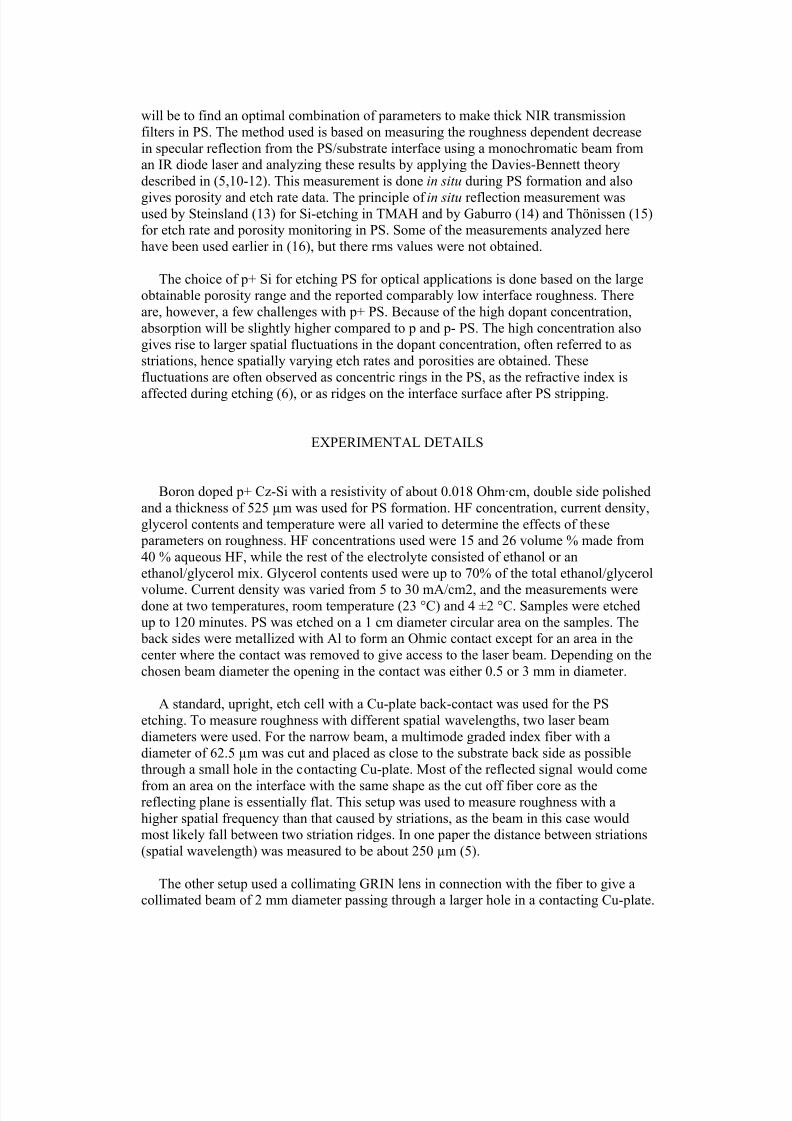
8/12/2019 Graded Optical Filters
http://slidepdf.com/reader/full/graded-optical-filters 96/164
will be to find an optimal combination of parameters to make thick NIR transmission
filters in PS. The method used is based on measuring the roughness dependent decrease
in specular reflection from the PS/substrate interface using a monochromatic beam froman IR diode laser and analyzing these results by applying the Davies-Bennett theory
described in (5,10-12). This measurement is done in situ during PS formation and alsogives porosity and etch rate data. The principle of in situ reflection measurement was
used by Steinsland (13) for Si-etching in TMAH and by Gaburro (14) and Thönissen (15)for etch rate and porosity monitoring in PS. Some of the measurements analyzed here
have been used earlier in (16), but there rms values were not obtained.
The choice of p+ Si for etching PS for optical applications is done based on the largeobtainable porosity range and the reported comparably low interface roughness. There
are, however, a few challenges with p+ PS. Because of the high dopant concentration,
absorption will be slightly higher compared to p and p- PS. The high concentration also
gives rise to larger spatial fluctuations in the dopant concentration, often referred to as
striations, hence spatially varying etch rates and porosities are obtained. Thesefluctuations are often observed as concentric rings in the PS, as the refractive index is
affected during etching (6), or as ridges on the interface surface after PS stripping.
EXPERIMENTAL DETAILS
Boron doped p+ Cz-Si with a resistivity of about 0.018 Ohm·cm, double side polished
and a thickness of 525 µm was used for PS formation. HF concentration, current density,
glycerol contents and temperature were all varied to determine the effects of these
parameters on roughness. HF concentrations used were 15 and 26 volume % made from40 % aqueous HF, while the rest of the electrolyte consisted of ethanol or an
ethanol/glycerol mix. Glycerol contents used were up to 70% of the total ethanol/glycerolvolume. Current density was varied from 5 to 30 mA/cm2, and the measurements were
done at two temperatures, room temperature (23 °C) and 4 ±2 °C. Samples were etched
up to 120 minutes. PS was etched on a 1 cm diameter circular area on the samples. The back sides were metallized with Al to form an Ohmic contact except for an area in the
center where the contact was removed to give access to the laser beam. Depending on the
chosen beam diameter the opening in the contact was either 0.5 or 3 mm in diameter.
A standard, upright, etch cell with a Cu-plate back-contact was used for the PS
etching. To measure roughness with different spatial wavelengths, two laser beamdiameters were used. For the narrow beam, a multimode graded index fiber with a
diameter of 62.5 µm was cut and placed as close to the substrate back side as possiblethrough a small hole in the contacting Cu-plate. Most of the reflected signal would come
from an area on the interface with the same shape as the cut off fiber core as the
reflecting plane is essentially flat. This setup was used to measure roughness with a
higher spatial frequency than that caused by striations, as the beam in this case wouldmost likely fall between two striation ridges. In one paper the distance between striations
(spatial wavelength) was measured to be about 250 µm (5).
The other setup used a collimating GRIN lens in connection with the fiber to give a
collimated beam of 2 mm diameter passing through a larger hole in a contacting Cu-plate.

8/12/2019 Graded Optical Filters
http://slidepdf.com/reader/full/graded-optical-filters 97/164
The beam was oriented normal to the sample and the lens both collimated the incident
beam and collected the reflected beam. A sketch of the setup is shown in Fig. 1. A series
of experiments used a setup where the beam directed at the sample was not coupledthrough fiber. This free space laser interferometer has been described before (16).
Figure 1 Sketch of the measurement setup. A standard etch cell is modified so that an IR diode laser
(LD) beam may be directed from a multimode (MM) optical fiber towards the back side of the sample
and the reflected beam collected back into the fiber, either via a collimating GRIN lens (left image) or
by direct coupling (right). The return signal is returned by a 2x1coupler to a GaAs PIN detector. The
LD is first connected to a single-mode fiber with an optical isolator, then it is connected with one inputof the MM 2x1 coupler. While etching, the PS/substrate interface moves giving rise to interference in
the reflected beam.
An IR laser diode controlled to have constant temperature and power at a wavelengthof 1550 nm pigtailed to a single-mode optical fiber was used as a monochromatic,
coherent light source. At this wavelength Si is partially transparent. To minimize back
reflectance to the diode and keep the phase stable, optical isolators were added. At the
sample end the single mode fiber was connected to a multimode fused 2x1 coupler tomake back reflectance from the sample back side into the fiber end easier (large core) and
to facilitate reading of the reflected signal, see Fig. 1. A fiber coupled PIN GaAs
photodiode was used to detect the reflected signal.
For comparison, the roughness and surface profile of a few samples were measured by
white-light interferometry (WLI) (WYKO NT-2000). To cover as large area as possible
of the sample, a low resolution of 6.22 µm per pixel was chosen. This would filter outany high frequency component, but this kind of roughness was not expected to besignificant. These measurements were done after stripping the PS layer away by etching
in NaOH. To get a reasonable etching time with the thick layers, up to 200 µm, a
concentrated solution was used, even though this attacked the area around the PS as well.
THEORY AND METHOD
During etching, the reflected laser beam from the sample contains a combination of
beams partly reflected from several interfaces; sample backside, PS/substrate interface

8/12/2019 Graded Optical Filters
http://slidepdf.com/reader/full/graded-optical-filters 98/164
and PS/electrolyte interface. As the PS/substrate interface is moving an interference
pattern will appear in the signal. The analysis of this signal is based on the Short-Time
Fourier Transform method (STFT), which gives a time-resolved frequencydecomposition of the signal. From this it is possible to extract interferences between
different partially reflected beams. The principle is shown in Fig. 2 where the mostimportant beams and combinations are shown. The extracted frequencies and amplitudes
of the different interference signals give information on porosity, etchrate and interfacescattering (14,16). In Fig. 3 a spectrogram from one such STFT calculation is shown,
with traces of the two lowest order reflections shown as thick black lines and higher order
reflections shown as thin black lines. These two lower order traces correspond to the two
cases in Fig. 2. To obtain information on the PS/substrate interface roughness, theinterference between the beam reflected from the substrate backside and the beam
reflected specularly from the substrate/PS interface was chosen, corresponding to case 2
in Fig. 2
The intensity of the combined reflection of these two beams, I ref , is given by
)cos(222
PS sub PS sub PS subref A A A A I ϕ ϕ −++= , [1]
where A sub and A PS are the amplitudes and φ sub and φ PS are the phases of the beamsreflected from the substrate back side and the PS/substrate interface respectively. As the
optical path length of the beam within the substrate changes during etching, φ PS changes.
This will lead to an oscillation in I ref with a frequency given by dt d PS sub )( ϕ − . This
frequency may not be constant as the etch rate generally will change with time or depth.The cosine component of I ref gives the amplitude and frequency of this oscillation and is
traced in the spectrogram. The oscillation amplitude is given by the cosine prefactor. A sub is constant while A PS contains information on the PS/substrate interface scattering,
substrate absorption and PS refractive index (in the electrolyte):
air sub sub PS sub PS sub R sub subair PS t t t r t st t t A −−−−= )()()()()( , α α . [2]
Here t air-sub and t sub-air are the transmission amplitude coefficients, r sub-PS (t) the time
dependent reflection amplitude coefficient as the PS refractive index changes during
ethcing, s R,sub-PS (t) the time dependent scattering factor as the roughness changes withtime and α sub(t) the absorption factor which changes due to a decrease in substrate
thickness.
The scattering factor is calculated by fitting the extracted amplitude to a doubleexponential as in Fig. 4, where a reflection amplitude from a wide beam measurement has
been extracted from the spectrogram and fitted. Fitting is done to avoid fluctuationscaused by crossing, interfering signals in the STFT as can be seen in Fig. 3. The fitted
amplitude is then scaled so that the extrapolated value at t=0 corresponds to the
theoretical amplitude with zero scattering. The scaling is necessary because the measured
data are not normalized to unit reflectance. The STFT uses a movable windowingfunction which results in average amplitude values over the time range the window
covers, hence the STFT amplitude values for t=0 are correct for the signal at a time in the
middle of the first window. This necessitates an extrapolation of amplitude to t=0. The
fitted and scaled amplitude function corresponds to A PS (t). Transmission and reflection

8/12/2019 Graded Optical Filters
http://slidepdf.com/reader/full/graded-optical-filters 99/164
Figure 2 A diagram showing the reflected
beam composition. The reflected signal will
contain interference oscillations from thecombination of beams I and II (case 2) and
beams I and III (case 1) as well as other, higher
order combinations. For PS/substrateroughness analysis, the signal from case 2 is
extracted and used in calculations. This
corresponds to the upper main trace (thick line)
in the spectrogram in Fig. 3.
Figure 3 Spectrogram from STFT of an IR
reflectance signal from the back of a sampleduring PS etching. Thick black line indicates
traces of the two lowest order beam
interferences used for roughness, porosity andetch rate calculations, while thin black lines
indicate traces of higher order beam
interferences. The numbering of the traces
correspond to the two cases in Fig. 2.
amplitude coefficients, as well as the
absorption factor, are calculated using published data for the complex refractive
index of bulk Si. Normal Fresnel relations
are used for transmission and reflection
coefficients, while the absorption factor is
given by ( )λ π α )(2exp)( t kz t sub −= where k
is the imaginary part of the complex
refractive index and z(t) is the time
dependent substrate thickness.
Davies-Bennett theory (10,11) attempts
to describe the local phase change in thereflected plane wave front introduced by the
height irregularities of the interface. These
phase changes results in a reduced intensityin the specular direction as conditions fordestructive interference will develop
between different parts of the wave front.
The theory assumes an rms irregularity
height (roughness) value, σ , much smallerthan the wavelength of the incident light in
the medium, λ, and that the height function
describing the roughness has a Gaussian
distribution. In this case the Fresnelreflection coefficient for a perfectly flat surface, R0, may be altered to incorporate the
effect of interface scattering at an incident angle in the medium, θ sub:
0 10 20 30 40 50 600.00
0.02
0.04
0.06
0.08
0.10
0.12
0.14
A m p l i t u d e , a . u .
Time, min
Figure 4 Reflection amplitude from the upper trace
(marked 2) of a spectrogram equivalent to Fig. 3.The dotted line is the fitted double exponential done
to avoid amplitude fluctuations caused by
interfering signals.

8/12/2019 Graded Optical Filters
http://slidepdf.com/reader/full/graded-optical-filters 100/164
⎥⎥
⎦
⎤
⎢⎢
⎣
⎡
⎟⎟ ⎠
⎞⎜⎜⎝
⎛ −== −
−
2
0
0
2
,0cos
4exp
sub
sub PS sub PS sub R sub
n R s R R
θ λ
πσ ,
[3]
where n sub is the refractive index of the incident medium, λ0 the wavelength in vacuum
and σ sub-PS the PS/substrate interface roughness. Note that the spatial frequency of the
roughness does not enter into this equation, so both long period (striations) and short period (small scale) roughness will have an equal effect, depending only on σ sub-PS .
To calculate the rms roughness of the front surface, a scattering factor for
transmission, sT,sub-PS , must be calculated based on the obtained σ sub-PS . The transmissioncoefficient at the PS/substrate interface has been shown by Filiński (12) to be
⎥⎥⎥⎥
⎦
⎤
⎢⎢⎢⎢
⎣
⎡
⎟⎟⎟⎟
⎠
⎞
⎜⎜⎜⎜
⎝
⎛ ⎟ ⎠ ⎞
⎜⎝ ⎛
−−== −
2
0
0
2
,0
coscos2exp
λ
θ θ πσ PS
PS
sub
sub
PS subT sub
nnT sT T ,
[4]
for the same conditions as for the reflection coefficient in Eq. 3. Here T 0 is the
transmission coefficient for a perfect interface, while n PS is the refractive index of the PS
and θ PS is the angle in the PS layer. Then the reflected amplitude from the front becomes
air sub sub PS front PS front PS R PS PS sub PS subT sub subair front t t t t r t st t t t st t t A −−−−−−−= )()()()()()()()( ,
22
,
2 α α [5]
where most of the parameters are the same as in Eq. 2 with the addition of a timedependent transmission amplitude coefficient for the PS/substrate interface, t sub-PS (t), a
time dependent reflection amplitude coefficient for the PS/front interface, r PS-front (t), and
an absorption factor in the PS layer, α PS (t), defined as for α sub(t) with k PS calculated by
effective medium theory using the complex refractive index of bulk Si. The reflectedamplitude is given by the same calculations on the extracted amplitude of the signal in
case 1 in Figs. 2 and 3 as for A PS . The calculation of the scattering factor, s R,PS-front , is the
same as for s R,sub-PS and gives the rms roughness value at the front interface.
RESULTS
Temperature effect
Assuming that the reflectance measurements give a good estimate of the roughness atthe beam spot, and that the roughness in this limited area is an indication of both
roughness time evolution and the roughness of the whole sample, the data plotted in Fig.
5 shows that roughness of samples etched with 15 % HF are influenced by etchant
temperature while those samples etched with 26 % HF are not significantly influenced.The porosity and etchrate data for the 15 % samples are calculated and shown in Fig. 6,
as well as data for low temperature etching with 15 % HF and 1:9 glycerol:ethanol. There
is an increase in porosity and decrease of etch rate with decreased temperature. The

8/12/2019 Graded Optical Filters
http://slidepdf.com/reader/full/graded-optical-filters 101/164
porosity data describe the instantaneous porosity closest to the interface, and therefore
also gives a porosity profile of the PS layer with depth. When calculating these data the
dissolution of PS closer to the surface, i.e. chemical dissolution, has been disregarded asthis is very small for p+ PS. Note the sharper increase in the RT porosity profile
compared to the low temperature profile. A similar effect has been reported by Servidoriin (8) for PS in p-type Si.
0 20 40 60 80 100
0
20
40
60
80
100
120
140
26%,L
26%,RT
15%,LT
R o u g h
n e s s , r m s n m
Thickness, µm
15%,RT
Figure 5 Roughness dependence on temperature
for different HF concentrations. In the 15 % HF
case there is a decrease in roughness with
temperature while the 26 % HF case show no
such dependence.
0 20 40 60 80 100 120
0.55
0.60
0.65
0.70
0.75
0.80
0.85
0.6
0.8
1.0
1.2
1.4
P
o r o s i t y , a b s .
Time, min
15 % HF, LT, 0 % Gly
15 % HF, LT, 10 % Gly
15 % HF, RT, 0 % Gly
15 % HF, LT, 0 % Gly
15 % HF, LT, 10 % Gly
E t c h
r a t e , µ m / m i n
15 % HF, RT, 0 % Gly
Figure 6 Comparison of porosity and etch rate between low temperature (4 °C) and RT etched
samples, with electrolyte consisting of 15 % HF and
0 % or 10 % glycerol. Current density used was 15
mA/cm2 for all three.
Glycerol effect
The effect of replacing 10 % of the ethanol volume with glycerol on roughness at lowtemperature is shown in Fig. 7 where a 15 % HF solution is used. In this case roughness
increases with the added glycerol compared to roughness measured without. A
comparison with results obtained at RT, shown in Fig. 9, may indicate an explanation.
These samples are etched with varying glycerol percentage from 0 to 70 % and HFconcentrations of 15 and 26 %. It is evident that a significant decrease in roughness is
obtained when replacing 10 % ethanol with glycerol at RT in the 15 % HF case. At lowtemperature the viscosity of the electrolyte increases compared to at RT. By adding 10 %
glycerol to the electrolyte at low temperature, the viscosity increases further and theroughness evolution is comparable to the evolution with a glycerol content higher than 10
% at RT. In Fig. 9 it is evident that roughness increases with glycerol content above 10
%. As seen for the low temperature porosity and etch rate data in Fig. 6, there is very
little difference between the samples with and without glycerol. This differs from thesame situation at RT in Figs. 8 and 9, where roughness decreases, porosity increases and
etch rate decreases by adding 10 % glycerol.
For other glycerol concentrations than 10 % in the 15 % HF case, the effect of addingglycerol is minimal. Below 25 µm the roughness is greatest with no glycerol and

8/12/2019 Graded Optical Filters
http://slidepdf.com/reader/full/graded-optical-filters 102/164
0 10 20 30 40 500.50
0.55
0.60
0.65
0.70
0.75
0.80
0.9
1.0
1.1
1.2
1.3
1.4
P o r o s i t y , a
b s .
Time, min
10 % Gly
0 % Gly
0 % Gly
10 % Gly
E t c h r a t e , µ m
/ m i n
Figure 8 Porosity and etch rate obtained by reflectionmeasurements showing the dependence on
temperature and time. Samples were etched at RTwith a 15 % HF solution.
0 20 40 60 80 100
0
20
40
60
80
100
120
140
160
15%, 10 % Gly.
15%, 0 % Gly.
R o u g h n e s s , r m s
n m
Thickness, µm
Figure 7 Rms roughness plotted vs. PS layerthickness. There is a change in the roughness
evolution when adding glycerol to a 15 % HF
electrolyte at low temperature. Samples are
etched at 15 mA/cm2.
decreases with decreasing glycerol concentration from 70 % and down, however, for
higher concentrations of glycerol or no glycerol at all the roughness seems to stabilize,
while for lower concentrations of glycerol the roughness steadily increases with PSthickness. A similar comparison is done in the 26 % HF case. Here the final roughness
increases with increasing glycerol concentration, with the sample etched with no glycerol
having the lowest roughness, although for thicknesses up to about 20 µm the electrolyte
with 20 % glycerol gives the lowest roughness.
HF concentration, current density effect and roughness saturation
Comparing the data for 15 and 26 % HF in Fig. 9 a general tendency is apparent, most
of the data for 26 % HF shows a lower rms roughness than for 15 % HF, with the
exception of the 15 % HF + 10 % glycerol plot. However, HF concentration is reported tohave no effect on roughness in p and p- PS (5). When etching with 15 % HF and 10 %
glycerol and changing current density from 5 to 30 mA/cm2 a smaller spread in roughness
values is obtained compared to the same experiment done with no glycerol (16). In fact,at a 20 µm PS layer thickness the rms roughness varies from 30 to 70 nm with 10 %glycerol and from 40 to 110 nm without. However, there is no apparent systematic effect
of current density on roughness in these data. This differs with the case of etching whit a
26 % HF solution. Here the roughness seems to increase with current density. At 60 µm
thickness rms values are 66 nm, 75 nm and 92 nm for 10, 20 and 30 mA/cm2
respectively. According to (5), roughness decreases with an increase in current density in
p and p- PS.

8/12/2019 Graded Optical Filters
http://slidepdf.com/reader/full/graded-optical-filters 103/164
0 20 40 60 80
0
20
40
60
80
100
120
0 20 40 60 80
0 % Gly
20 % Gly
30 % Gly
40 % Gly R o u g h n e s s , r m
s n m
Thickness, µm
26 % HF
0 % Gly
10 % Gly
20 % Gly
30% Gly
70 % Gly
15 % HF
Figure 9 Comparison of
rms roughness data fordifferent combinations of
HF concentrations and
glycerol amounts. All
samples are etched at RTand with 10 mA/cm2.
In (5) two distinct regimes are shown to exist in the roughness evolution for p and p-
type PS. With roughness plotted against layer thickness in a log-log plot, it is clear that
roughness enters a saturation regime after a linearly increasing regime. In the datadiscussed here, roughness clearly increase faster in the beginning, however, in a log-log plot some show a clear correspondence with the two-regime picture, while some are
closer to linear. In Fig. 10 a sample etched at RT in 15 % HF with 10 mA/cm2 shows a
saturation regime while a sample etched with 20 mA/cm2 does not show any such
saturation. The saturation regime is explained as a result of a transition from hole limitedto a diffusion limited etching. A diffusion limited etching will be dominant when
diffusion of reaction species is decreased due to increased thickness of the porous layer,
hence fluctuations in resistivity at the PS/substrate interface have no influence on hole
availability and an asperity smoothening effect occurs. Another indication of the changein diffusion is the porosity depth profile and etch rate change with time obtained for all
the samples investigated in this study, as in Figs. 6 and 8.
1 10 10010
20
30
40
50
60
708090
100
15 %HF, 0 % Glycerol, RT, 20 mA/cm2
R o u g
h n e s s , r m s n m
Thickness, µm
15 %HF, 0 % Glycerol, RT, 10 mA/cm2
Figure 10 Plot of roughness showing clearly the
increase and the saturation regime in the low current
case, and the lack of saturation in the high current
case. Both samples etched in 15 % HF at RT without
glycerol. The line is only a guide for the eye.
The effect of spot size
By using different beam widths it is possible to probe different roughness
spatial wavelengths which are not
accounted for in Eq. 3. The period of the
striations as reported in (5) and WLI
measurements reported here, is in theorder of a few hundred µm. By using a
spot size large enough to cover several ofthese oscillations, good statistics are
obtained on the scattering effect.
However, a spot size smaller in diameter
than the striation wavelength, as obtainedwith a cut fiber end giving effectively a
62.5 µm spot, will not be scattered much
by this roughness. Only roughness of
shorter wavelengths will scatter the
incident light. By using this spot size it

8/12/2019 Graded Optical Filters
http://slidepdf.com/reader/full/graded-optical-filters 104/164
was not possible to obtain a value for the rms roughness, indicating that short period
roughness was below the detection limit of about 10 nm (5) roughness determination by
specular reflection, hence practically all of the surface irregularity is caused by striations.
Roughness of the PS/electrolyte interface
Analysis of the PS/electrolyte interface roughness was attempted. As explained in the
theory and method part, both the signal from case 1 and case 2 in Figs. 2 and 3 are used
to obtain this roughness. Due to the small roughness (<10 nm) at this interface asreported by Servidori et al. (8), no reliable data were obtained. The absorption in PS
during etching will likely be large due to H2 bubble formation during etching of PS, this
is not accounted for in the calculation of the absorption factor.
Comparison between reflection and WLI
measurement
To verify that the method of roughness
calculation by specular reflection gives a good
indication of roughness, WLI measurementswere performed on a few samples that were
stripped of PS. A 2 mm diameter circular area
in the center of the samples where the laser
beam was thought to have been, was extractedfrom the WLI data. The rms roughness values
from these areas are compared to themaximum roughness values obtained by
reflection in Table 1 and show an excellent fit.
The true position of the beam is not known, sothese values are only indicative of what is
likely. These samples were all etched for long
times, up to 130 minutes, and were therefore quite deep, 200 µm. Figure 11 shows a
surface plot of one such measurement. The parallel ridges caused by striations are clearlyvisible. The rms roughness values obtained by this method show a very strong positional
dependence with a total rms value over the whole etched area up to a factor 2 larger thanthat measured by reflection.
Figure 11 Surface plot of PS/substrateinterface height data obtained by WLI
measurement. Parallel ridges with at least two
distinct spatial repeatability wavelengths areclearly visible. These are caused by slightly
different etch rates due to inhomogeneities in
resistivity, i.e. striations. Rms irregularity
height is in this case about 180 nm.
Figure 11 indicates that the roughness has several spatial wavelengths. A comparably
small period roughness, with a wavelength of about 200 µm in the direction normal to the
ridges, is evident in the smaller ridges in the surface plot, as well as a much larger period
roughness with a wavelength in the order of mm. This large period roughness is veryirregular compared with the smaller and gives rise to the positional dependence of the
discussed WLI measurements, but both are most likely caused by an irregular dopant
distribution. The rms roughness values for the whole etched area are also tabulated in
Table 1. Note that this value is obtained after correcting for interface curvature, which is
caused by an inhomogeneous current distribution due to the opening in the Al back

8/12/2019 Graded Optical Filters
http://slidepdf.com/reader/full/graded-optical-filters 105/164
contact and the design of the etch cell. This was done by an algorithm in the WYKO
analysis program. The large period roughness was not observed in WLI measurements
done on similar samples etched much shorter, to depths of about 10 µm. At this depth,only striations similar to the short period ones in Fig. 11 were present, and the rms
roughness was a few tenths of nm. This may indicate a slower development of the longwavelength roughness.
Table 1 Comparison between measured roughness rms values by reflectance, data from a 2 mm diameter
circular area at the center of each sample with white light interferometry (WLI) and data from the whole
sample by WLI. LT is low temperature (4 °C) and RT is room temperature. Note that thicknesses will not
be the same for different samples.
Sample
number
Etch condition Small area
WLI (nm)
Reflectance
measurement(nm)
Full area
WLI (nm)
46 26%HF,15mA/cm2,RT,100min 157 157 272
47 15%HF,15mA/cm2,RT,120min 173 170 336
48 26%HF,15mA/cm2,RT,120min 168 169 273
52 26%HF,15mA/cm2,LT,120min 155 153 42953 26%HF,30mA/cm
2,LT,120min 187 186 339
Reflection measurements will give a good indication of the roughness caused by
striations of short period, but not of the longer period roughness. This is probablysatisfactory when monitoring the interface quality of optical elements with small feature
sizes, of the order of the beam diameter, or when etching PS layers some tens of µm
thick, however, to monitor the roughness evolution of interfaces larger than a few mm in
diameter a wider incident beam is needed.
Plots of calculated rms roughness values vs. depth from the reflectance measurements
for the samples that were analyzed withWLI are shown in Fig. 12. The data
obtained for 26 % HF show a remarkable
consistency. It seems the roughnessevolution does not depend on current
density or temperature. The full area WLI
data do not follow the same trends,
however, indication that the larger periodroughness is affected by the parameters in
a different way. Perhaps there is a
maximum correlation length over which
saturation of roughness is achieved, whilefor distances larger than this there is little
correlation between diffusion constants in
the electrolyte or local hole concentration
at the interface.
0 80 160
0
80
160
R
o u g h n e s s , r m s n m
PS layer thickness, µm
15%RT 15 mA
26%RT/5 deg/15 and 30 mA
Figure 12 Rms roughness calculated from reflection
measurements comparing the influence of
temperature, HF concentration and current density.DISCUSSION AND CONCLUSION
There seems, as shown, as if there is only a very narrow region of parameter space
where an increase in electrolyte viscosity by addition of glycerol is beneficial for

8/12/2019 Graded Optical Filters
http://slidepdf.com/reader/full/graded-optical-filters 106/164
PS/substrate interface roughness in p+ PS, and even this is different for room temperature
and low temperature. All the parameters studied may affect the viscosity of the
electrolyte, or rather reaction species diffusion, as has been suggested (7,8). However, itseems a too high “diffusion constant” increases roughness and the same for a too low
“constant”, at least in the case of p+ PS. The reduction of roughness seems to be limitedto a factor of maximum two for fairly thick layers. Substrate quality is of importance, as
the roughness discussed here is more or less completely dependent on dopantdistribution. It seems more difficult to control roughness of p+ PS compared to what has
been published on p and p- PS.
The laser reflection interference roughness measurement method presented in this paper gives a good estimate of the roughness rms value within the laser beam spot,
whether this value is representative for the whole sample depends on the spatial
wavelength of the roughness. In the case of some of the p+ Si wafers used in this study,
dopant variations with several wavelengths are present in WLI measurements, at least
with wavelengths of about 200 µm and 1 mm. This may explain some discrepancies orunexpected results within the presented data. PS/substrate roughness on a smaller scale
(micro-roughness) and low rms value striation roughness are undetectable with the
presented method. This is in agreement with other reports stating that microscaleroughness is very small at a p+ PS/substrate interface and that specular reflection
methods are reliably for rms roughness larger than 10 nm. There are both similarities and
differences between roughness progression in p+ PS and other p-type PS. There areindications of a saturation regime for some of the samples, where the rms roughness
value increases little more with PS layer depth, while for others a saturation regime was
not reached within the measurement time/depth.
REFERENCES
1. H. Man-Lyun, K. Jae-Ho, Y. Sung-Ku and K. Young-Se, IEEE Phot. Tech. Lett., 16, 1519
(2004).
2. V. Mulloni, L. Pavesi, Appl. Phys. Lett., 76, 2523 (2000).
3. G. Vincent, Appl. Phys. Lett ., 64, 2367 (1994).
4. M. G. Berger, C. Dieker, M. Thönissen, L. Vescan, H. Lüth, H. Münder, W. Theiß, M. Wernke
and P. Grosse, J. Phys. D, 27, 1333 (1994).
5. G. Lérondel, R. Romestain and S. Barret, J. Appl. Phys., 81, 6171 (1997).
6. G. Lérondel, P. Reece, A. Bryant and M. Gal, Mat. Res. Soc. Symp. Proc., 797, 15 (2004).
7. S. Setzu, G. Lérondel and R. Romestain, J. Appl. Phys., 84, 3129 (1998).
8. M. Servidori, C. Ferrero, S. Lequien, S. Milita, A. Parisini, R. Romestain, S. Sama, S. Setzu
and D. Thiaudière, Solid State Comm., 118, 85 (2001).9. X.G. Zhang, J. Electrochem. Soc., 151, C69 (2004).
10. H. Davies, Proc. Inst. Electr. Eng., 101, 209 (1954).
11. H.E. Bennett and J.O. Porteus, J. Opt. Soc. Amer ., 51, 123 (1961).
12. I. Filiński, Phys. Stat. Sol. (b), 49, 577 (1972).
13. E. Steinsland, T. Finstad and A. Hanneborg, J. Electrochem. Soc., 146, 3890 (1999).
14. Z. Gaburro, C.J. Oton, P. Bettotti, L. Dal Negro, G. Vijaya Prakesh, M. Cazzanelli and L.
Pavesi, J. Electrochem. Soc., 150, C281 (2003).
15. M. Thönissen, M.G. Berger, S. Billat, R. Arens-Fischer, M. Krüger, H. Lüth, W. Theiß, S.
Hillbrich, P. Grosse, G. Lerondel and U. Frotscher, Thin Solid Films, 297, 92 (1997).
16. P.Y.Y. Kan, S.E. Foss, T.G. Finstad, Phys. Stat. Sol. a/c (in press).

8/12/2019 Graded Optical Filters
http://slidepdf.com/reader/full/graded-optical-filters 107/164
Chapter 5
Filter fabrication
The goal of producing multilayer structures, or refractive index modulatedstructures, by porosification of silicon, is to add the possibility of controllinglight, its spectral composition, phase, and movement, through a device.In this thesis the focus of the ”device” fabrication is on the control of the spectral component of incident light, while many of the findings andtechniques may be used for other elements within silicon photonics.
The principles of optical filter design has been described earlier in Chapter 3.From these principles we may draw the conclusion that a good refractiveindex control, layer thickness control, and maximum interface smoothness
is imperative to obtain filters of good quality. In PSM fabrication thistranslates to control of porosity with depth and time, control of etch ratewith depth and time and minimization of interface roughness. To a certaindegree the control, or at least a knowledge of, the microtopology of theporous structure and the relation to refractive index is also necessary asdiscussed in Sec. 3.1.
A specific goal of this thesis has been to obtain good quality IR opticalfilters of different kinds in PS. A parallel goal has been to use the flexibilityof PSM fabrication to extend the usability of the standard filter. In thecase of graded filter structures the obtained quality of the filters depends
strongly on the level of understanding of flat filter fabrication in PS as somequality will be lost to the extra design freedom obtained. Ideally, a filtersspectral features will become sharper with an increasing number of layers.This assumes no or very weak absorption. With PS, this is possible in theIR, especially for wavelengths around 1500 nm where the absorption is ata minimum.
To list some of the points we must take care of to be able to fabricate goodquality PSMs:
• Porosity must be known.
• Etch rate must be known.
97

8/12/2019 Graded Optical Filters
http://slidepdf.com/reader/full/graded-optical-filters 108/164
98
• PS morphology should be known.
• Change in parameters/factors during etching (as a function of time,
depth, etch area geometry, structural ”history”) should be known.• A model for calculating the effective refractive index as a function of
porosity (and morphology) must be known.
• The transition of effective refractive index across an interface betweentwo layers should be understood and controlled.
• The roughness of an interface should be understood and controlled.
• The effect of chemical etching of the porous structure should be takenaccount of.
• A good understanding of the etching process is helpful; where and how(only pore tip or partly up the walls of the pore, oxidation, passiva-tion by hydrogenation of walls etc., the effect of incident light duringetching and bubble formation).
Most of these points have been or will be addressed in this thesis. Thosepoints not addressed are assumed to play relatively small roles in the overallresults, however, they are still likely to be measurable.
5.1 Basic filter etching
As a first approximation to filter etching, we may assume that the obtainedporosity during etching is only dependent on the applied current densityand the given etch conditions. Likewise, the etch rate may be assumedconstant with time and layer depth and only dependent on current density.A standard way of obtaining these data is to etch several samples at differentcurrent densities for a given depth or for a given time. Porosity may bemeasured by gravimetry and etch rate may be derived from the etched
thickness which may be obtained by SEM or profilometry. From these dataa porosity versus current density curve and etch rate versus current densitycurve may be plotted. The porosity curve fits well with a log function of the type:
P ( j) = P 0 + γ ln
j
β + 1
, (5.1)
where P ( j) and P 0 are the current density dependent and constant con-tribution porosities respectively, j is the current density and γ and β arefitting parameters. Porosity vs. current density data with a fit using Eq. 5.1is shown in Fig. 5.1. The data was obtained from etching p+ samples in
13.3 % HF for 60 seconds at room temperature. The fit parameters in thiscase are P 0=15, γ =6.5 and β =1.6. A similar approximation to the etch
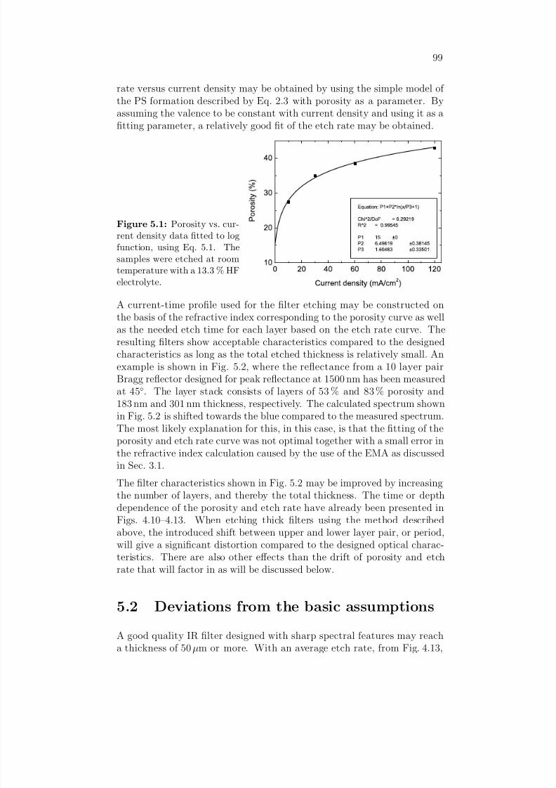
8/12/2019 Graded Optical Filters
http://slidepdf.com/reader/full/graded-optical-filters 109/164
99
rate versus current density may be obtained by using the simple model of the PS formation described by Eq. 2.3 with porosity as a parameter. Byassuming the valence to be constant with current density and using it as a
fitting parameter, a relatively good fit of the etch rate may be obtained.
Figure 5.1: Porosity vs. cur-rent density data fitted to logfunction, using Eq. 5.1. Thesamples were etched at roomtemperature with a 13.3 % HFelectrolyte.
A current-time profile used for the filter etching may be constructed onthe basis of the refractive index corresponding to the porosity curve as wellas the needed etch time for each layer based on the etch rate curve. Theresulting filters show acceptable characteristics compared to the designedcharacteristics as long as the total etched thickness is relatively small. Anexample is shown in Fig. 5.2, where the reflectance from a 10 layer pair
Bragg reflector designed for peak reflectance at 1500 nm has been measuredat 45. The layer stack consists of layers of 53 % and 83 % porosity and183 nm and 301 nm thickness, respectively. The calculated spectrum shownin Fig. 5.2 is shifted towards the blue compared to the measured spectrum.The most likely explanation for this, in this case, is that the fitting of theporosity and etch rate curve was not optimal together with a small error inthe refractive index calculation caused by the use of the EMA as discussedin Sec. 3.1.
The filter characteristics shown in Fig. 5.2 may be improved by increasingthe number of layers, and thereby the total thickness. The time or depth
dependence of the porosity and etch rate have already been presented inFigs. 4.10–4.13. When etching thick filters using the method describedabove, the introduced shift between upper and lower layer pair, or period,will give a significant distortion compared to the designed optical charac-teristics. There are also other effects than the drift of porosity and etchrate that will factor in as will be discussed below.
5.2 Deviations from the basic assumptions
A good quality IR filter designed with sharp spectral features may reacha thickness of 50 µm or more. With an average etch rate, from Fig. 4.13,
8/12/2019 Graded Optical Filters
http://slidepdf.com/reader/full/graded-optical-filters 110/164
100
Figure 5.2: Reflectance of aBragg reflector designed for apeak reflectance at 1500 nm.Consists of 10 pairs of lay-ers of 53% and 83% porosityand 183 nm and 301 nm thick-ness respectively. No adjust-ment of current density withtime was used. A shift of themeasured spectrum comparedto the calculated spectrum ispresent. Filled squares denotemeasured spectrum and opencircles denote the calculated
design spectrum.
of about 1.5 - 2 µm/min, this thickness is reached after about 25 - 35 min.The change in porosity and etch rate may be substantial within this time.This should be taken into account in the design of the current profile.
Besides the drift in porosity and etch rate with time which is suggested inSec. 4.2.4 to be caused by limitations in diffusion of electrolyte species to andfrom the etch front, a change in temperature during etching may also intro-duce a change in porosity and etch rate from the expected values. Anothereffect is the chemical etching discussed briefly in Sec. 4.2.1. These factors
may influence both the etching of each filter as well as the reproducibil-ity of filter etching. The etch cell geometry may also have a small effecton reproducibility as the Pt-electrode may be positioned slightly differentfor each etch, thereby changing the potential distribution and possibly thestructure, however, this variation has not been quantized.
5.2.1 Effect of HF diffusion
A closer look at the HF diffusion is in order. Because of a finite system
to start with and a finite, limiting diffusion of reaction species to and fromthe etch front caused by the porous structure, the electrolyte compositionwill change in the active region, i.e. etch front, during etching. This willintroduce a change in etch rate, structure and porosity with time. How thisinfluences the fabrication of filters is quite complex.
As F− ions are bound to Si following the reaction in Eq. 2.1, more HFmolecules are dissociated and new HF molecules diffuse toward the etchfront. In effect, the HF concentration changes at the etch front, alwaysdecreasing during etching with a constant current. There are two mainfactors controlling the HF concentration at the etch front; the usage of F−-
ions, mainly give by the current density, but also by the valence, and thediffusion of HF molecules to the etch front, given by a diffusion constant

8/12/2019 Graded Optical Filters
http://slidepdf.com/reader/full/graded-optical-filters 111/164
101
and the concentration gradient. The valence is sensitive to current density,temperature and HF concentration. The diffusion coefficient function islikely to be dependent on the electrolyte properties, e.g. viscosity, as well
as on the porous structure.
In this discussion a couple of factors are not taken into account, namely theeffect of a finite electrolyte reservoir and the behavior of other electrolytespecies, especially those resulting from the reactions at the etch front. Asimplification in a discussion like this would be to assume that the HFconcentration at the surface of the PS is constant, however, with a finitereservoir without stirring this is not likely to be the case. A constant surfaceconcentration of HF could probably be used as a first approximation in amodel, however. The behavior of other electrolyte species will most likelybe linked to the HF concentration and not be rate limiting in themselves. Inan empirical model it should be possible to only use the HF concentrationand diffusion coefficient as the electrolyte parameters.
We may assume that the changes in etch rate and porosity with time alreadyshown in the constant current plots are only due to changes in the electrolytecomposition at the etch front. Thus, according to the discussion above, itshould be possible to correlate each porosity value at any given time to astarting porosity for a certain HF concentration. However, to project thetime evolution of etch rate and porosity, the microtopology must also beknown, as this will influence the HF diffusion.
In Fig. 4.9 the complicating effect of different microtopologies on the poros-ity evolution for otherwise equivalent parameters is shown. This has a sig-nificant effect on the etching of multilayer structures. The effect of changingthe current density from high to low will be twofold: the concentration atthe etch front will most likely be lower than if the layer had been etchedat the same low current density for the same amount of time, this is dueto the higher usage of HF. However, the concentration also depends on thediffusion which will be higher because of a steeper gradient and because thepores are larger. The diffusion to the etch front will be higher compared toa constant low current density etch which means that the evolution of thefollowing etch will be different.
To get an idea of the effect this drift in porosity and etch rate will have onPS optical filters we may use the thick Bragg mirror mentioned above asan example. Say that we make one filter where the current densities usedfor both high and low refractive index are constant throughout the etchingassuming that there is no drift in etch parameters. For a layer etched at38 mA/cm2 to get a porosity of 80 % (n=1.32) for 6 s to get a thickness of 200 nm, at the top of the filter, a layer etched with the same current densityand etch time after 30 min of etching will give a layer of about 90 % porosity
(n=1.14) and a thickness of 190 nm, shifting the wavelength fulfilling theBragg condition λBragg = 4nd (Bragg wavelength) by an amount given by

8/12/2019 Graded Optical Filters
http://slidepdf.com/reader/full/graded-optical-filters 112/164
102
(assuming small changes):
∆λcenter = 4 (n ∆d + ∆n d) . (5.2)
Inserting the above values gives a shift of about 200 nm. When the Braggwavelength shifts from front to back in a Bragg mirror the resulting re-flectance band broadens and ”chirps”.
5.2.2 Effect of temperature
For all chemical reactions, temperature is an important factor. Etchingof PS is no exception. The kinetics of the reaction at the etch front willchange with temperature as well as the diffusion of the different electrolytespecies. With an increasing temperature the diffusion is affected by both adecrease in viscosity and a higher thermal activity of the diffusing species.An example of this is shown in the comparison of etch rates and porositiesobtained at two different temperatures in Figs. 5.3 and 5.4. The samplesmeasured here were fabricated by etching for 100 to 120 min at 15 mA/cm2
in an electrolyte consisting of 26 % HF and ethanol. The temperaturesused were 4±1 C and 23±1 C. Two samples were etched for each set of parameters several days apart, both measurements at each temperature areshown in the plot. The reproducibility seems quite good, the greatest ad-verse effect on the reproducibility probably being temperature variations
during etching. After 100 min etching the data for the same temperaturesshow a 1.6-1.7 % relative difference. The relative difference between the4 and 23 C plots in etch rate after 100min is 17.8% with the etch rateincreasing with temperature, while for the porosity the relative differenceis 9.2 % with the porosity decreasing with temperature. If we assume alinear temperature dependence, the relative difference for the etch rate is0.93%C−1 and for the porosity it is 0.48 %C−1. These values are largeenough to possibly explain the difference between the two measurementsat the same temperature as being due to small temperature differences. Inabsolute values this translates to 16.8 (nm/min)C−1 for the etch rate and
-0.32 %(abs)
C−1
for the porosity. For simplicity we may approximate thedifference in refractive index between two porosities with a linear relation.In the IR a 1 %(abs) difference in porosity would yield a (3.8-1)/100=0.028difference in refractive index. Hence, the change in refractive index with in-creasing temperature is 0.0090 C−1. Notice that both the etch rate changeand the refractive index change result in an increase in optical thicknesswith increasing temperature for a constant current density.
For a Bragg reflector in the IR with a low index layer of 60% porosity(n=1.84) etched for 10 s (nominally 200 nm thick), the shift in reflectanceband center wavelength due to a change in the optical thickness of this layer,
using the values found above and Eq. 5.2 would be about 28 nm/
C. Thisis obviously a significant shift which shows that temperature control during

8/12/2019 Graded Optical Filters
http://slidepdf.com/reader/full/graded-optical-filters 113/164
103
etching of PSMs is important. These calculations only hold for the case of 15 mA/cm2 current density with the described electrolyte. The tempera-ture dependence of PS etching will most likely depend on the electrolyte
composition and the current density.
Figure 5.3: Measured etch rateas a function of time for four sam-ples etched under the same condi-tions, 15 mA/cm2 with 26% HF,but at two different temperature aslabeled. Note the reproducibility of the results for similar temperatures.The etch rate increases with temper-ature.
Figure 5.4: Measured porosity asa function of time for four samplesetched as in Fig. 5.3. The porositydecreases with temperature whichmeans that the refractive index in-creases with temperature.
As current passes through the electrolyte and the sample, resistive heatingwill occur. This will in the same way as above introduce changes in etchrate and porosity, but in this case the changes occur during etching. Thetemperature was measured together with the data shown in Figs. 4.10–4.13showing the temperature change due to resistive heating and ambient tem-perature variations. In Fig. 5.5 the temperature profiles measured duringconstant current etching with 70, 30, and 5 mA/cm2 in 15% HF with 10%
glycerol, at room temperature are shown. One would expect that the tem-perature change would be dependent on the current density with resistiveheating. This is observed in Fig. 5.5 with the 70 mA/cm2 etching increasingin temperature from ≈18 C to ≈23 C, while the 30 mA/cm2 etching has afairly stable temperature. The decrease in temperature for the 5 mA/cm2
etching is most likely due to a decrease in ambient temperature. This etchcurrent dependent temperature change is likely to have a significant impacton optical filter characteristics. The obtained temperature evolution willdepend on the current profile needed for each specific PSM. Following thediscussion relating to temperature differences between etches, a change in
temperature from start to finish of 5
C during etching of a Bragg mirrorcould result in a substantial ”chirping” or broadening of the filter optical

8/12/2019 Graded Optical Filters
http://slidepdf.com/reader/full/graded-optical-filters 114/164
104
response due to a shift of ∼140 nm in the Bragg wavelength between frontand back.
Figure 5.5: Temperature vs.
time for selected samples alsoused in Figs. 4.11 and 4.13.Curve A was measured dur-ing etching with 70 mA/cm2,curve B with 30 mA/cm2 andcurve C with 5 mA/cm2. Theresistive heating is evident inthe 70 mA/cm2 case while thetwo other cases are closer to athermal balance with the en-vironment. The reason for
the temperature decrease inthe 5 mA/cm2 case is likelyto be a change in ambienttemperature.
5.2.3 Chemical etching
Chemical etching has been briefly discussed in Sec. 4.2.1. The change inrefractive index in p+ Si due to this effect should be small, but for very
good quality PS filters in p+ Si it may still be significant. To take chemicaletching into account, the porosity profiles obtained by the in situ reflectancemethod must be calculated with this in mind. When calculating a currentprofile for filter etching, an iterative process may be adopted where thea profile is calculated disregarding chemical etching, the total time eachlayer is in the etchant is calculated and subsequently the change in porositydue to chemical etching. Next, a new profile is calculated attempting tocounteract the porosity change due to chemical etching.
Assuming that the oscillation in the signal shown in Fig. 4.4 is a result of chemical etching, we have in this case (4.3 C, 30mA/cm2 and 26% HF
) that the average porosity of the film changes from 72.6 to 73.2 % over12.5 min. For simplicity we assume that the corresponding refractive indexchange (in air) is independent of porosity and constant, hence we have aconstant refractive index change due to chemical etching of 2 · 10−5s−1.The topmost layer in a Bragg mirror, similar to the one discussed above,will then have a change in refractive index due to long exposure (∼30 min)to the electrolyte. This change would be about 0.036 in this case. Thiswould shift the reflection band center wavelength about 7 nm. Chemicaletching has been reported to depend strongly on the substrate used as theobtained microtopology will change with doping. The dependence on HF
concentration is also significant [86] with higher concentrations resulting inless etching. There will most likely be a temperature dependence as well.

8/12/2019 Graded Optical Filters
http://slidepdf.com/reader/full/graded-optical-filters 115/164
105
5.3 Etch calibration
To improve the control of porosity and layer thickness during filter etching
compared to the basic filter etching discussed above in Sec. 5.1, the constantcurrent porosity and etch rate curves will be used to take into account thedrift of these parameters with time.
A first approximation to a complete calibration of a current profile may be toassume that the observed drift in the constant current plots is independentof etch history or microtopology and dependent only on time and currentdensity. Thus the needed current density at a given time for a given porosityis obtained by taking a slice from the porosity constant current plot at thegiven time and interpolating the porosities to get a porosity vs. currentdensity plot from which the current density is obtained. To obtain a currentdensity profile for filter etching, this is done for any number of discrete timesteps depending on the wanted time resolution. The necessary duration ateach porosity depends on the corresponding etch rate which is found in asimilar way. When the current density is found, this is used to find theetch rate in an interpolated etch rate versus current density plot. For eachtime step the total etched thickness and layer thickness is calculated. Whenthe designed layer thickness is reached, the porosity is changed accordingto the design. By using small enough time steps a good approximation tothe designed refractive index profile is reached. However, there will to somedegree always be discretization errors with this method.
A porosity versus current density versus time plot for the 15 % HF, 10 %glycerol electrolyte at room temperature is shown in Fig. 5.6. The data arethe same as in Fig. 4.11 but interpolated and smoothed. Comparing withFig. 5.1, it is clear that the porosity versus current plots for given times arenot as smooth. This is most likely due to the observed variation in ambienttemperature as well as resistive heating during etching.
Figure 5.6: The smoothedporosity vs. time and cur-rent density used for etch cur-rent profile calculation. Thedata used are the same as inFig. 4.11.
One way to take into account the etch history when calculating the currentprofile for a filter, is to shift the time axis in the constant current data

8/12/2019 Graded Optical Filters
http://slidepdf.com/reader/full/graded-optical-filters 116/164
106
in Figs. 4.10–4.13 with an amount depending on the current density. Wemay assume that the high current density etch will be the controlling factorfor HF concentration at the etch front. If the etching starts with a high
current density etched layer, the etch front HF concentration at the end of this etch will correspond to a concentration at a much later time for a lowercurrent density etch due to greater HF usage, hence the time axis is shiftedcompared to the constant current plot. We may assume that the changein etch front concentration is negligible for the low current etch, hence theetching at the next high current density layer picks up at the same timethe last high current density etch stopped. A change in concentration dueto the low current etch may also be taken into account by shifting thetime axis of the high current density etch correspondingly. The necessaryadded shift may be found by fitting the reflectance data for a PSM structure
etched assuming no drift in etch parameters with a model describing theseeffects, where the time axis shift is a fitting parameter. In this conceptualmodel it is assumed that etch front HF concentration is always decreasing,however this may not be correct in all situations. Changing from high tolow current density may result in an increase in HF concentration due tohigher diffusion than usage. This calculation has not been implemented forcurrent profile calculations, but, as will be shown below, the idea has beenused to understand some measured reflectance spectra.
In all the examples and discussions above the emphasis has been on discretefilters. This is only due to the ease of illustration, the same arguments apply
to the case of an inhomogeneous, e.g. rugate, filter, especially when this isapproximated by a number of discrete layers.
5.4 Prepared filters
5.4.1 Reflectance measurement setup
The reflectance experiments were performed with a standard setup utilizing
a monochromator to resolve the spectral components of the light reflectedfrom the sample. The setup is shown in Fig. 5.7. A broad band quartztungsten halogen lamp was used as a light source. The beam from thelamp was collimated and polarized, if necessary, and sent through a chop-per and an iris, for beam narrowing, before being reflected off the sample oran Al-mirror as a reference. The reflected light was collected by a lens andpassed through a monochromator (SpectraPro 275 by Acton Research Cor-poration) using either a 600 line/mm or a 1200 line/mm diffraction gratingdepending on the wavelength range measured. At the output a standard Sior Ge detector was placed, depending on the wavelength range measured.
The reflectance spectrum measured from a sample was normalized to thespectrum measured from the Al-mirror.
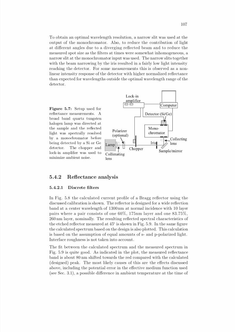
8/12/2019 Graded Optical Filters
http://slidepdf.com/reader/full/graded-optical-filters 117/164
107
To obtain an optimal wavelength resolution, a narrow slit was used at theoutput of the monochromator. Also, to reduce the contribution of lightat different angles due to a diverging reflected beam and to reduce the
measured spot size as the filters at times were somewhat inhomogeneous, anarrow slit at the monochromator input was used. The narrow slits togetherwith the beam narrowing by the iris resulted in a fairly low light intensityreaching the detector. For some measurements this is observed as a non-linear intensity response of the detector with higher normalized reflectancethan expected for wavelengths outside the optimal wavelength range of thedetector.
Figure 5.7: Setup used forreflectance measurements. Abroad band quartz tungstenhalogen lamp was directed atthe sample and the reflectedlight was spectrally resolvedby a monochromator beforebeing detected by a Si or Gedetector. The chopper andlock-in amplifier was used tominimize ambient noise.
5.4.2 Reflectance analysis
5.4.2.1 Discrete filters
In Fig. 5.8 the calculated current profile of a Bragg reflector using thediscussed calibration is shown. The reflector is designed for a wide reflectionband at a center wavelength of 1300 nm at normal incidence with 10 layer
pairs where a pair consists of one 60%, 175nm layer and one 83.75%,260 nm layer, nominally. The resulting reflected spectral characteristics of the etched reflector measured at 45 is shown in Fig. 5.9. In the same figurethe calculated spectrum based on the design is also plotted. This calculationis based on the assumption of equal amounts of s- and p-polarized light.Interface roughness is not taken into account.
The fit between the calculated spectrum and the measured spectrum inFig. 5.9 is quite good. As indicated in the plot, the measured reflectanceband is about 80 nm shifted towards the red compared with the calculated(designed) peak. The most likely causes of this are the effects discussed
above, including the potential error in the effective medium function used(see Sec. 3.1), a possible difference in ambient temperature at the time of

8/12/2019 Graded Optical Filters
http://slidepdf.com/reader/full/graded-optical-filters 118/164
108
Figure 5.8: The calculatedcurrent profile used to obtainthe filter measured in Fig. 5.9.Note the change in high andlow current with time.
Figure 5.9: Reflectance of aBragg reflector (filled squares)with a designed reflectanceband center at 1300 nm. Thereflector consists of 10 pairsof layers, each pair consistingof a 83.75% layer and a 60%layer, nominally. The mea-surement is made at 45 usingunpolarized light. The calcu-lated reflectance is shown withopen circles. The measuredreflectance is shifted relativeto the calculated spectrum,which is also shown shifted forillustration (dashed line).
etching compared to the calibration data and the use of a simplified modelfor calibration. A red shift indicates optically thicker layers; physicallythicker and/or lower porosity. The observed shift of about 80 nm could beaccounted for by a difference in porosity of about 5 % (absolute difference)
compared to the designed value. This number compares well with the dis-cussion in Sec. 3.1 and above. There are other features in the spectrumindicating that the current profile is not perfectly adjusted for the effectof electrolyte species diffusion. A distortion in the spectrum may also becaused by the striation induced lateral inhomogeneity of the filter if thebeam spot is large enough, which is the case with the spot size of about1 mm used for most of the reflection measurements.
Figures 5.2, 5.10 and 5.11 compare reflection spectra from Bragg reflectorsdesigned to reflect at 1500 nm. The spectrum in Fig. 5.2 is from a structureconsisting of 10 pairs of layers with nominally 53 % and 83 % porosities and
thicknesses of 183 and 301 nm, respectively, etched without time calibration.The peak is shifted about 80 nm towards the red from the designed peak
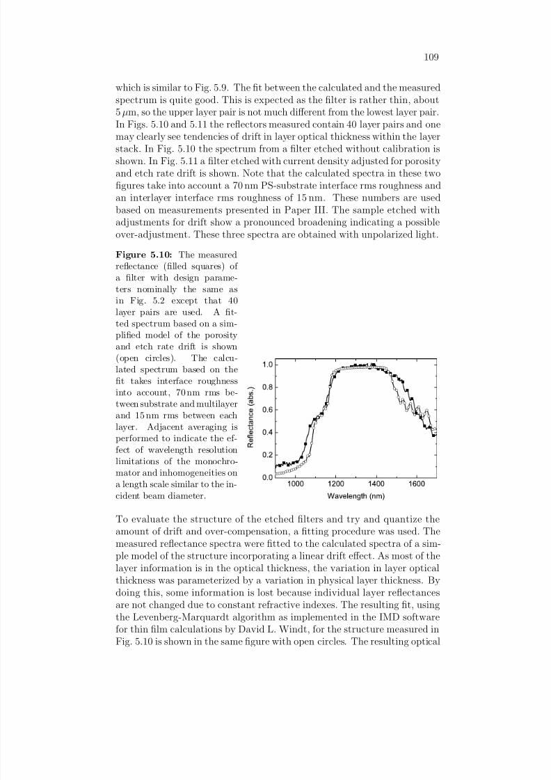
8/12/2019 Graded Optical Filters
http://slidepdf.com/reader/full/graded-optical-filters 119/164
109
which is similar to Fig. 5.9. The fit between the calculated and the measuredspectrum is quite good. This is expected as the filter is rather thin, about5 µm, so the upper layer pair is not much different from the lowest layer pair.
In Figs. 5.10 and 5.11 the reflectors measured contain 40 layer pairs and onemay clearly see tendencies of drift in layer optical thickness within the layerstack. In Fig. 5.10 the spectrum from a filter etched without calibration isshown. In Fig. 5.11 a filter etched with current density adjusted for porosityand etch rate drift is shown. Note that the calculated spectra in these twofigures take into account a 70 nm PS-substrate interface rms roughness andan interlayer interface rms roughness of 15 nm. These numbers are usedbased on measurements presented in Paper III. The sample etched withadjustments for drift show a pronounced broadening indicating a possibleover-adjustment. These three spectra are obtained with unpolarized light.
Figure 5.10: The measuredreflectance (filled squares) of a filter with design parame-ters nominally the same asin Fig. 5.2 except that 40layer pairs are used. A fit-ted spectrum based on a sim-plified model of the porosityand etch rate drift is shown(open circles). The calcu-lated spectrum based on the
fit takes interface roughnessinto account, 70 nm rms be-tween substrate and multilayerand 15 nm rms between eachlayer. Adjacent averaging isperformed to indicate the ef-fect of wavelength resolutionlimitations of the monochro-mator and inhomogeneities ona length scale similar to the in-cident beam diameter.
To evaluate the structure of the etched filters and try and quantize theamount of drift and over-compensation, a fitting procedure was used. Themeasured reflectance spectra were fitted to the calculated spectra of a sim-ple model of the structure incorporating a linear drift effect. As most of thelayer information is in the optical thickness, the variation in layer opticalthickness was parameterized by a variation in physical layer thickness. Bydoing this, some information is lost because individual layer reflectancesare not changed due to constant refractive indexes. The resulting fit, usingthe Levenberg-Marquardt algorithm as implemented in the IMD software
for thin film calculations by David L. Windt, for the structure measured inFig. 5.10 is shown in the same figure with open circles. The resulting optical

8/12/2019 Graded Optical Filters
http://slidepdf.com/reader/full/graded-optical-filters 120/164
110
Figure 5.11: The measuredreflectance (filled squares) of a filter with design parame-ters nominally the same as inFig. 5.10 except that the cur-rent profile is adjusted accord-ing to the calibration proce-dure discussed. A calculatedspectrum based on the designis shown (open triangles). Afitted spectrum base on a sim-plified model of the porosityand etch rate drift is shown(open circles). The calculation
based on the fit takes inter-face roughness into account,30 nm rms between substrateand multilayer and 5 nm rmsbetween each layer.
Figure 5.12: The result-ing bragg wavelength (opti-cal thickness×4) of the layersof the filter corresponding to
Fig. 5.10 after fitting a sim-plified model to the measuredspectrum. The drift in poros-ity and etch rate with timeis assumed to result in a lin-ear change in optical thicknesswith depth in this model.
thickness for each layer, transformed to Bragg wavelengths (4×optical thick-ness), is shown in Fig. 5.12. The resulting spectrum fits the measurement
quite well. Note that adjacent averaging is used with the fitted spectrumto simulate the effect of wavelength resolution limitations in the monochro-mator. The layer optical thicknesses shown in Fig. 5.12 show that there isa marked drift in optical thickness which may be caused by one or both of etch rate and porosity drift. The optical thickness of all the layers shouldhave been the same according to the design, in this case corresponding toa Bragg wavelength of 1500 nm, but the resulting optical thicknesses differquite markedly between high and low porosity layers. This may be thatthe starting point of the etch was incorrect, i.e. that either the calibrationcurves were slightly off true value because of e.g. temperature differences, orthat the effective medium function introduced an error as discussed earlier.
The same procedure was performed for the filter measured in Fig. 5.11. The

8/12/2019 Graded Optical Filters
http://slidepdf.com/reader/full/graded-optical-filters 121/164
111
Figure 5.13: Same asFig. 5.12 for the case where thecurrent profile was calibrated(Fig. 5.11).
resulting fitted spectrum is shown in the same figure with open circles. Notall features seem explained, but the widening and the general band edgegradients seem explained quite well. Figure 5.13 shows the layer Braggwavelengths of the fitted spectrum. It is clear that the calibration procedurehas had a significant effect on the structure. The low porosity layers seemmost affected by the calibration, while the high porosity/high current layersseems well adjusted and nearly constant throughout the structure. Thismay indicate that a time shift of the calibration curves when designing afilters is appropriate. The etch rate decrease or porosity increase with timefor the low porosity layers seem much stronger than that taken into account.
5.4.2.2 Rugate filters
Rugate filters were fabricated in the same manner with a time calibrationdone on the current profile. In Figs. 5.14 and 5.15 the measured and calcu-lated reflection spectra are shown for two fabricated rugate reflectors. Thesample used for Fig. 5.14 was designed for a narrow reflection band at 600nm. Index matching was used while no apodization was used. The porosityvaried from 49 % to 53 % nominally between the index matching regions.The filter contained 65 periods in the refractive index profile resulting in athickness of about 10 µm. A low temperature of about 6 C was used along
with an aqueous electrolyte consisting of 26 % HF and ethanol. The lowtemperature was used in an attempt to minimize roughness as discussed inPaper III. The values of the measured data are only indicative as a base-line was subtracted from the data as very a low light intensity resulted ina non-linear detector response. The same trend as discussed for the othermeasured spectra is present in Fig. 5.14 with the measured spectrum red-shifted compared to the calculated spectrum, however the band shapes arequite similar, with a measured full width at half maximum of 10 nm, indicat-ing little drift of porosity and etch rate. The effect of interface roughness isclearly seen comparing the two calculated spectra; one taking into account
interface roughness, one without roughness. In Fig. 5.15 the reflectance of athick IR rugate filter is measured. This filter was designed with a medium

8/12/2019 Graded Optical Filters
http://slidepdf.com/reader/full/graded-optical-filters 122/164
112
width reflection band at 1550 nm with 75 periods in the refractive index,both index matching and quintic apodization were used. The total thick-ness was about 30 µm. A time calibration of the current profile was done in
this case also. This filter was etched at low temperature (4
C) with a 26%HF electrolyte. A calculated spectrum based on the design is shown. It isevident that the refractive index profile is not optimal as the peak is muchtoo wide and non-uniform. To test the suggestion that this widening is dueto a drift in the layer optical thickness as discussed, a calculation of thereflection spectrum with a linear increase in the period was done. This isshown as a dashed line in Fig. 5.15. The correspondence is good indicatingan over-adjustment due to a non-optimal calibration. In both Figs. 5.14and 5.15 the calculated spectra shown in whole line are without roughnesstaken into account, while the calculations shown in dashed lines are with a
rms roughness at the interface of 70 nm and an interlayer rms roughness of 15nm.
Figure 5.14: The measuredreflectance spectrum (filledsquares) of a rugate reflectancefilter designed for a narrowpeak at wavelength of 600 nm.The calculated spectrum with(solid curve, open circles) andwithout (dashed curve) an rms
interface roughness of 70 nmis shown also. Both mea-surement and calculations arefor an incident angle of 45.The same red shift is presenthere as in most other filtersmeasured.
In Fig. 5.16 the measured reflectance spectrum of a three band rugate spec-trum is shown. The filter was designed as a narrow band pass filter with awide blocking band on both sides of the pass band. This was done similar
to the design calculated in Fig. 3.14 with three reflectance bands very closeto each other. The calculated current profile, adjusted for drift in porosityand etch rate, is shown in Fig. 5.17. The regions in the current profile cor-responding to the different bands overlap in such a way as to minimize thethickness without allowing the total refractive index to go over a certainthreshold value. The lower current values reach a limiting threshold severalplaces whereby the current is clipped. This procedure introduces some fea-tures in the spectral characteristics, however, with little clipping the resultis acceptable. As can be seen in Fig. 5.16 the main spectral characteristicsin the designed filter are recognizable in the measured spectrum. Again,
due to roughness and overcompensation for drift, the result is not optimal.Note that the calculated spectrum in this case is only for s-polarized light.

8/12/2019 Graded Optical Filters
http://slidepdf.com/reader/full/graded-optical-filters 123/164
113
Figure 5.15: A thick ru-gate reflection filter is com-pared with calculated spectra.The design was for a peakat 1550 nm, using 75 refrac-tive index periods with porosi-ties varying between 30 % and53 %. The etch current pro-file was adjusted for drift re-sulting seemingly in an over-compensation. A calculatedspectrum incorporating a shiftin design peak wavelength isshown as the dashed red curve.
This compares well with themeasured spectrum.
Figure 5.16: Reflectancemeasurement of a three peakrugate filter (filled squares).The filter was designed to havea narrow transmittance bandas can be seen in the cal-
culated spectrum (open cir-cles). The calculated spec-trum is for s-polarized lightwhile the measurement is un-polarized. The pass band ispresent in the measured spec-trum, but much wider than de-signed due to drift in porosityand etch rate with depth andinterface roughness.
Etch brakes have been used quite successfully by Billat et al. [87] and Reeceet al. [59]. The etch breaks allows the electrolyte at the etch front toregenerate, avoiding problems caused by diffusion of the electrolyte species.However, the etch time of a filter increases substantially compared with acontinuous etch as typically break times are in the order of 10 to 20 timesthe time it takes to etch the thickest of the layers in the layer pair [88]. Thisresults in an etch time of about one hour for a 20 layer pair Bragg stack
with peak wavelength at 1300 nm. By increasing the etch time this muchthe effect of chemical etching must be considered, even for p+ samples.
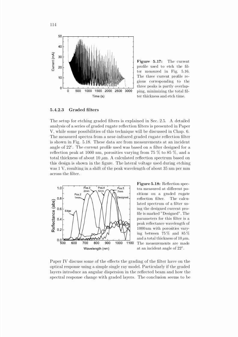
8/12/2019 Graded Optical Filters
http://slidepdf.com/reader/full/graded-optical-filters 124/164
114
Figure 5.17: The currentprofile used to etch the fil-ter measured in Fig. 5.16.The three current profile re-gions corresponding to thethree peaks is partly overlap-ping, minimizing the total fil-ter thickness and etch time.
5.4.2.3 Graded filters
The setup for etching graded filters is explained in Sec. 2.5. A detailedanalysis of a series of graded rugate reflection filters is presented in PaperV, while some possibilities of this technique will be discussed in Chap. 6.The measured spectra from a near-infrared graded rugate reflection filteris shown in Fig. 5.18. These data are from measurements at an incidentangle of 22. The current profile used was based on a filter designed for areflection peak at 1000 nm, porosities varying from 75 % to 85 %, and atotal thickness of about 10 µm. A calculated reflection spectrum based on
this design is shown in the figure. The lateral voltage used during etchingwas 1 V, resulting in a shift of the peak wavelength of about 35 nm per mmacross the filter.
Figure 5.18: Reflection spec-tra measured at different po-sitions on a graded rugatereflection filter. The calcu-lated spectrum of a filter us-ing the designed current pro-file is marked ”Designed”. The
parameters for this filter is apeak reflectance wavelength of 1000 nm with porosities vary-ing between 75 % and 85 %and a total thickness of 10 µm.The measurements are madeat an incident angle of 22.
Paper IV discuss some of the effects the grading of the filter have on theoptical response using a simple single ray model. Particularly if the graded
layers introduce an angular dispersion in the reflected beam and how thespectral response change with graded layers. The conclusion seems to be

8/12/2019 Graded Optical Filters
http://slidepdf.com/reader/full/graded-optical-filters 125/164
115
the errors introduced by an angular dispersion in the incident beam over-shadows any effect of the graded layers.
An indication of the regularity of the periods of the fabricated filters may
be obtained by high resolution field emission SEM (FESEM) images. Fig-ure 5.19 shows a cross-section FESEM image of the reference (non-graded)rugate reflection filter presented in Paper V. The average image intensityprofile taken across the image is overlayed in yellow. A sine like profile isclearly recognizable. The obtained sine profile is not accurate enough toshow a difference in period from top to bottom which seems present whenconsidering the ”chirping” of the spectral responses of the filters in thepaper.
Figure 5.19: Cross-sectionSEM of a rugate reflection fil-ter. The measured reflectancespectrum of this filter is pre-sented in Paper V. A plot of the average pixel intensity val-ues in the gray scale SEM im-age taken parallel to the sur-face is shown to the right,overlayed on the image. The
sinusoidal intensity variationcoincides with the designed re-fractive index variation.
5.5 Improvements of the process
Several potential and known causes of errors in the PSM structures havebeen discussed. Some possible remedies for these problems are suggestedin the following:
• stirring to keep sample surface electrolyte composition constant aswell as reduce temperature gradients/changes, pump induced flow forthe same reasons or bubling of e.g. nitrogen gas.
• temperature control of electrolyte (main volume) and of sample.
• introduce breaks in etching to regain original electrolyte compositionin active region as briefly discussed.
• the effect of bubble formation in pores during etching may be reduced
by using a different wetting agent (may be improved further comparedwith ethanol).

8/12/2019 Graded Optical Filters
http://slidepdf.com/reader/full/graded-optical-filters 126/164
116
• (micro-) roughness may be reduced by a limited viscosity increase(lower temp or addition of glycerol) as indicated in Papers II and III.
• use a cathode integrated in the etch cell to keep the position constantrelative to the sample.

8/12/2019 Graded Optical Filters
http://slidepdf.com/reader/full/graded-optical-filters 127/164
IV
Paper IV
S.E. Foss and T.G. FinstadMultilayer interference filters with non-parallel in-
terfaces
Proceedings of the Nordic Matlab Conference,Copenhagen, Denmark, 2003

8/12/2019 Graded Optical Filters
http://slidepdf.com/reader/full/graded-optical-filters 128/164

8/12/2019 Graded Optical Filters
http://slidepdf.com/reader/full/graded-optical-filters 129/164
Æ

8/12/2019 Graded Optical Filters
http://slidepdf.com/reader/full/graded-optical-filters 130/164
Æ
Æ

8/12/2019 Graded Optical Filters
http://slidepdf.com/reader/full/graded-optical-filters 131/164
Æ
Æ
Æ
Æ
Æ
Æ
Æ
Æ
Æ
Æ
Æ
Æ
Æ

8/12/2019 Graded Optical Filters
http://slidepdf.com/reader/full/graded-optical-filters 132/164
θ θ
B
A
C
1
2
3
4
5
6
7
Si-substrate
Graded PS film
Incidentbeam
Æ
Æ
Æ
Æ
Æ
Æ
Æ
Æ
Æ

8/12/2019 Graded Optical Filters
http://slidepdf.com/reader/full/graded-optical-filters 133/164
Æ
Æ
Æ
Æ
Æ
Æ

8/12/2019 Graded Optical Filters
http://slidepdf.com/reader/full/graded-optical-filters 134/164

8/12/2019 Graded Optical Filters
http://slidepdf.com/reader/full/graded-optical-filters 135/164
V
Paper V
S.E. Foss and T.G. FinstadLaterally graded rugate filters in porous silicon
Mat. Res. Soc. Symp. Proc., 797, W1.6.1 2004

8/12/2019 Graded Optical Filters
http://slidepdf.com/reader/full/graded-optical-filters 136/164

8/12/2019 Graded Optical Filters
http://slidepdf.com/reader/full/graded-optical-filters 137/164
Laterally Graded Rugate Filters in Porous Silicon
Sean E. Foss and Terje G. Finstad
Department of Physics, University of Oslo,POBox 1048 Blindern, 0316 Oslo, Norway
ABSTRACT
Rugate optical reflectance filters with position dependent reflectance peaks in the visible to
near infrared spectrum were realized in porous silicon (PS). Filters with strong reflection peaks,
near 100%, no detectable higher order harmonics and suppressed sidebands compared to discretelayer filters were obtained by varying the current density continuously and periodically during
etching. An in-plane voltage up to 1.5 V was used to obtain refractive index and periodicity
change along the filter surface resulting in reflectance peak shifts of up to 100 nm/mm in the
direction of the voltage drop. The effect of the lateral change in optical parameters on the filtercharacteristics is studied by varying the gradient and comparing measurements at different
positions with measurements on a non-graded filter. We have observed extra features in thereflectance spectrum of these graded filters compared with reflectance from a non-graded filter
which is likely caused by the gradient.
INTRODUCTION
The process of discretely varying the current density during etching of porous silicon (PS) to
obtain thin layers with different refractive indexes was first reported by Vincent [1] and Berger
et al. [2] in 1994. With this method Bragg reflectors and Fabry-Perot filters are now routinelymade. By applying an in-plane voltage across the sample during etching, Hunkel et al. have
shown that it is possible to produce PS discrete filters with laterally dependent filtercharacteristics [3,4]. In addition to the discrete layer filters (i.e. Bragg and Fabry-Perot) one may
also realize structures in PS that are uniquely simple to this system. By varying the current
density continuously and periodically, the refractive index into the PS layer will vary accordingly[5]. The refractive index may be calculated from the porosity by the effective medium
approximation. With this approach one obtains reflecting rugate filters which may have narrow
reflection peaks, no higher order harmonics and suppressed sidebands. For an overview of rugatefilter theory, see Bovard [6]. Here we report on rugate filters with laterally varying
characteristics which have been made for the visible to near infrared optical spectrum.
EXPERIMENTAL DETAILS
The Si substrate used was 0.018Ω·cm B-doped, p-type Czochralski-grown single crystal
with <100> orientation polished on both sides. The HF-based solution used for etching consisted
of 1:2 HF(40 %):ethanol. The etching current was controlled by a computer, in this case with atime step of 1 second which sufficiently reproduced the refractive index sinusoid. The used
current profile is shown in Fig. 1. The etching occurs mostly at the pore tips which is why
porosity may be modulated by the current. There will also be a small chemical etching which is
W1.6.1Mat. Res. Soc. Symp. Proc. Vol. 797 © 2004 Materials Research Society

8/12/2019 Graded Optical Filters
http://slidepdf.com/reader/full/graded-optical-filters 138/164
dependent on time. This is corrected for by etching the deeper part of the layer with a slightly
higher current.The starting point for the design was a 1 cm diameter, circular, non-graded rugate filter with
a reflectance peak-wavelength at 738 nm measured with light incident at 24 deg. The filter was
made relatively thin with 23 periods of the porosity sinusoid over 5 µm. Etching was done withcurrent density varying between 9.4 mA·cm
-2 and 19.7 mA·cm
-2, which corresponds to refractive
indexes at the peak wavelength of 1.78 and 1.48 respectively. Index matching for the air-PS
interface and the PS-substrate interface was employed to reduce sidebands. This may beobserved in the beginning and end of the current profile of Fig. 1 where there are large slopes.
A schematic of the etching setup is shown in Fig. 2. A lateral gradient in porosities and etch
rates was obtained by applying a constant in-plane voltage up to 1.5 V between two contacts onthe sample back side while etching with the same current profile as for the starting point design.
By doing this the local current density varies. Ohmic contacts were made from evaporating Al on
the samples followed by a short heat treatment. The resistance between the contacts varied
between 0.6 and 0.7 Ω for the different samples. Contact resistance is a substantial fraction of
this, so good, reproducible contacts were important to achieve control of the potential drop
within the sample.
Reflectance measurements were conducted with a 0.275 m focal-length monochromator with
a Si-detector. The focused probe beam had a diameter of less than 1 mm and was directed at the
filter at an angle of about 24 deg. Both the size of the beam and the angle contribute to awidening of the reflectance peak to some extent compared to the peak from the non-graded filter.
The effect depends on the gradient of the filter. Reflectance spectra are only plotted from 600 nm
to 1100 nm because of the combination of the detector and diffraction grating used in themonochromator.
For the optical images a microscope with a mounted digital camera was used. Several images
were stitched together to get a better overview. To show the striation effects on the filter
Figure 1. Applied current during etching
of all filters. The slopes at the beginning
and end are for index matching.
Figure 2. Sketch of the etch setup. The Si
sample with Al back contacts is pressed on to
two Cu-plates on the back side so an in-planeconstant voltage can be set up. The current-
source is connected to a computer.
W1.6.2

8/12/2019 Graded Optical Filters
http://slidepdf.com/reader/full/graded-optical-filters 139/164
reflectance clearly in these images, the RGB colors were split into separate images and only the
green was used for analysis as this had the largest contrast between striation minimum andmaximum.
A white light interferometer, WYKO NT-2000 by Veeco, was used to measure surfacetopography profiles of the samples after the PS was stripped away with a concentrated NaOH
etch. This instrument has a large dynamical range and can measure µm and nm height
differences in the same measurement. Even with the gradient in the samples present,
measurements showing the ridges caused by striations, in the order of 100 nm high, werepossible.
RESULTS AND DISCUSSION
The reflectance spectrum of the non-graded starting point filter is shown in Fig. 3. Often
when designing rugate filters one employs apodization to further reduce sideband reflection [6].This was not done on the presently reported filters. Observed sidebands show a periodicity
dependent on the average optical thickness, n·d , of the PS film at the measured position whichmay be used to calculate the average refractive index. Because of the refractive index dispersion
in Si the sidebands in the reflectance plot will decrease in frequency with increasing wavelength.
Reflectance spectra at four different positions along a line through the center of a filter madewith an in-plane voltage of 1.0 V are shown in Fig. 4. Comparing these peaks with the one from
the non-graded filter in Fig. 3 it is clear that the grading affects the shape, width and height. The
position of the maximum reflected wavelength shifts along the filter as expected. The amplitudeof the maximum reflectance decreases towards shorter wavelengths. This is most likely due to
increased absorption [3]. There is also a broadening of the peaks away from the mid position
towards shorter wavelengths caused by the fact that the refractive index does not have a linear
Figure 3. Reflectance spectrum of a non-
graded rugate filter used as a starting point
for graded filters. Measurements are takenat 24 deg. incident angle. FWHM is 100
nm.
Figure 4. Plot of reflectance spectra from a
filter made with an in-plane voltage of 1.0 V.Marked positions are along a centerline across
the circular filter in the direction of the
gradient. Note the spreading of the peak as itmoves towards lower wavelengths.
W1.6.3

8/12/2019 Graded Optical Filters
http://slidepdf.com/reader/full/graded-optical-filters 140/164
dependence on current density [3]. Therefore the amplitude and period in the refractive index
sinusoid will only be optimal at one point along the filter surface. All the graded filters showsimilar behavior. A decrease of amplitude between samples with increasing grading is also
observed. This is most likely caused by the finite spot size of the probe beam. When this covers atoo large area compared to the gradient at that point, the resulting measurement will be anaverage of spectra and hence the filter window will be smeared out.
Figure 5 shows the peak wavelengths at different positions for a series of filters with
changing in-plane voltage. As expected, the shift increases with the voltage caused by theincrease in the porosity and etch rate gradient. The horizontal line across the plot shows the peak
wavelength of the non-graded filter. The reflectance peak is clearly not at 738 nm for the mid
position for any of the graded filters. Thus the current density does not vary linearly withposition. This is as expected considering the geometry of the etch setup.
Although the shift in peak wavelength seems close to linear, depth profiles of the PS layer
made by white light interferometry after stripping, shown in Fig. 6, show tendencies towards
non-linearity. This is also supported by [7] where Bohn and Marso describe an equivalent circuitmodel for the etch situation. A non-linear current density distribution will result in a varying
position of the crossing point between the peak shift curves and the non-graded peak wavelength.One would, however, expect that at some point the filter would have the characteristics of the
non-graded filter as the total current is the integral of the local current density at all positions on
the filter area. This is true for the filters of Fig. 5 except for the 0.1 V case. A slight difference inprocess parameters is most likely the cause. In Fig. 7 the change in peak shift with applied in-
plane voltage is shown. The line corresponds to a linear fit which seems appropriate for this
range of voltages. A non-linearity might be expected for higher voltages as the necessary current
Figure 5. The wavelength of reflection peaksmeasured at different positions on samples with
different gradients, () for an in-plane voltage of
0.1 V, () for 0.5 V, () for 1.0 V and () for1.5 V. The shift of the peaks increases with
increasing in-plane voltage.
Figure 6. Depth profiles of the PS-substrate
interface measured with white lightinterferometry after removal of the PS layer.
One clearly sees the increasing gradient with
in-plane voltage. Curves are composed ofseveral single measurements stitched together
which cause drift in measured height, therefore
only tendencies are discussed.
0 2 4 6 8 10 12
-10
-8
-6
-4
-2
0
D e p t h ,
µ m
Distance from edge of filter, mm
1.5 V
0.1 V
0.5 V
W1.6.4

8/12/2019 Graded Optical Filters
http://slidepdf.com/reader/full/graded-optical-filters 141/164
reaches amperes, hence heating will probably affect the process. The geometry of the filter has
an effect on the local current density, as may be observed visually. Perpendicular to the gradientdirection reflection colors shift somewhat away from the center line, indicating a non-constant
current density towards the edges.Visible stripes of slightly different colors are present in all the filters made. These seem
circular and centered around the center of the 4” wafers used for samples. After stripping away
the PS with an NaOH etch these stripes are still present as ridges. Figure 8 shows a compilation
of a light microscope image representing the intensity of the green component from a colorimage (to increase contrast) and the subsequent intensity plot of the 2-dimensional height profile
from white light interferometry measurements at the same position after stripping of PS. Peak to
peak height of the ridges are about 100 nm. These ridges indicate locally different etch rates.Similar results have been reported earlier by Lérondel et al. [8] as likely being caused by
striations, i.e. radially symmetric resistivity inhomogeneities in the substrate due to an
inhomogeneous dopant distribution. One way of smoothing the PS-substrate interface is
suggested by Setzu et al. [9] where etching is done at low temperatures down to -35 C.
CONCLUSION
We have shown it is possible to make a laterally graded rugate filter with good reflectance.The filter may be improved by optimizing the parameters used, especially by using a smaller
difference between minimum and maximum refractive index and more periods, hence a thicker
PS film. Apodization may also be used to optimize the reflectance characteristics. Striationscausing locally differing etch rates have been shown.
Figure 7. Plot showing the rate of change of
the shift of the reflection maximum along thegrading of the filters as a function of applied
voltage.
Figure 8. Image of the 0.1V filter with an
overlay (between the two white crosses) of
an intensity plot of the correspondingsurface topography profile of the PS-
substrate interface measured by white light
interferometry. The white square in theintensity plot is missing data.
W1.6.5

8/12/2019 Graded Optical Filters
http://slidepdf.com/reader/full/graded-optical-filters 142/164
ACKNOWLEDGMENTS
This work has been carried out under the MOEMS and MEMS research program of theResearch Council of Norway. The authors would like to thank Maaike Taklo Wisser at SINTEF
for help with the WYKO measurements, and H. G. Bohn at Forschungszentrum Jülich, Germany,
for help with the program for designing the rugate filter.
REFERENCES
1. G. Vincent, Appl. Phys. Lett . 64, 2367 (1994).
2. M. G. Berger, C. Dieker, M. Thönissen, L. Vescan, H. Lüth, H. Münder, W. Theiss, M.
Wernke and P. Grosse, J. Phys. D: Appl. Phys. 27, 1333 (1994).3. D. Hunkel, R. Butz, R. Arens-Fischer, M. Marso and H. Lüth, J. Lumin. 80, 133 (1999).
4. D. Hunkel, M. Marso, R. Butz, R. Arens-Fischer and H. Lüth, Mater. Sci. Eng. B 69-70, 100(2000).
5. M. G. Berger, R. Arens-Fischer, M. Thönissen, M. Krüger, S. Billat, H. Lüth, S. Hilbrich, W.
Theiss and P. Grosse, Thin Solid Films 297, 237 (1997).6. B. G. Bovard, Applied Optics 32, 5427 (1993).
7. H. G. Bohn and M. Marso, (unpublished report).
8. G. Lérondel, R. Romestain and S. Barret, J. Appl. Phys. 81, 6171 (1997).9. S. Setzu, G. Lérondel and R. Romestain, J. Appl. Phys. 84, 3129 (1998).
W1.6.6

8/12/2019 Graded Optical Filters
http://slidepdf.com/reader/full/graded-optical-filters 143/164
Chapter 6
Porous silicon applications for
MOEMS and passive optics
The techniques and results presented in this thesis may be considered aspart of a toolbox to build novel devices in silicon microtechnology. Somepossibly new and untested ideas will be presented in the following show-ing some of the many possibilities of porous silicon as an optical material.The two main areas these ideas describe are passive optical elements andmicro-opto-electro-mechanical-systems (MOEMS). Several different passiveoptical elements and applications have been presented in the literature,some of which have been mentioned in Sec. 2.1. In the area of MOEMSthere are very few reported devices employing PS as a critical ”material”.The most striking device is the spectrometer by Lammel [89].
6.1 Passive optical elements
Passive optical elements are here thought of as elements made with PSwhere no activation is needed for them to work , neither by absorbed lightnor by an applied current/voltage. Such elements may be, e.g. lenses andfilters. One example of an active device would then by a PS-light emittingdiode (LED).
6.1.1 Schottky barrier spectroscopic IR detector
One aim of the presented work has been to prepare graded optical band-passfilters in PS, which for example could be used in a monolithically integratedsensor-array system. A fairly simple sensor design could be based on severalseparate Schottky barrier sensors on the back side with the graded bandpass filter, either Fabry-Perot or rugate, on the front side. This detector
would be for use in the near- to mid-IR as photons with wavelengths belowthe absorption edge of the silicon substrate would be absorbed and would
133

8/12/2019 Graded Optical Filters
http://slidepdf.com/reader/full/graded-optical-filters 144/164
134
not reach the Schottky barrier sensors. The sensors would be in the form of parallel strips with the length of each strip perpendicular to the filter gradi-ent direction. In this way each strip would respond to a specific transmitted
band of photon wavelengths, with the position of each strip relative to thefilter deciding which band will be detected. The total of the strips wouldthan give a spectroscopic detector. A schematic drawing of the design isshown in Fig. 6.1.
To obtain sharp features in the filter spectral characteristics, many layers orperiods are needed resulting in fairly thick filters. This necessitates a verygood control of etch rate, porosity and interface roughness. A standardBragg reflector of 50 layer pairs with a peak reflecting wavelength of 1.5 µmwould have a total thickness of roughly 20 µm. Reasonable filter thicknessesfor more complex rugate filters may reach 50 µm. The good control of the
parameters is also necessary to minimize some of the problems introducedby grading the filter.
The Schottky barrier sensor strips may be fabricated by different metalsdepending on the wavelength range of interest. Deposition of Ti, Ir andPt with a subsequent annealing produces silicides with low enough workfunctions so that photons not absorbed by the substrate may induce acurrent. The possible wavelength range of the detector is determined onthe high energy side by the absorbtion edge of the Si substrate, about1.1 eV, and on the low energy side by the barrier height, which for Al onp-type Si is about 0.55 eV and for PtSi on p-Si is normally 0.3 eV, but has
been reported for special cases to be as low as 0.13 eV [90]. This resultsin a detectable wavelength range from 1.127 µm to 2.254 µm for Al andfrom 1.127 µm to 4.133 µm or 9.5 µm for PtSi. The performance of such aspectroscopic detector would depend on the filter gradient and number andwidth of the sensor strips for wavelength resolution and on the filter sizeand Schottky barrier material for wavelength range.
By miniaturizing each element it may be possible to fabricate arrays of such detectors, with each identical detector detecting a range of discretewavelength bands. One would then have an imaging IR spectroscopic de-vice. Instead of basing the sensing on the Schottky effect, one may usepyroelectric materials, such as BaTi, for heat sensitive detector arrays. Itis possible to use PS on the contact side also. Raissi and Far reported inRef. [91] that electroplating of Pt within the pores of PS with a subsequentanneal produces Schottky barrier diodes with low barrier height and highefficiency.
6.1.2 2D photonic crystal
A subject of much research recently has been photonic crystals. A multi-
layer thin film optical filter can be said to be a 1D photonic crystal with aphotonic band gap, or forbidden band, i.e. reflection band. 2D and even

8/12/2019 Graded Optical Filters
http://slidepdf.com/reader/full/graded-optical-filters 145/164
135
Figure 6.1: A conceptual sketch of a Schottky barrier spectroscopic IRdetector. The graded band-pass rugate filter on the front of the substrateis fabricated as described earlier and optimized for transmission of near tomedium infrared photons. On the back side, Al or another fitting metal isdeposited. The metal-silicon junction forms a Schottky barrier which willemit charge carriers when hit by photons within a certain energy range. Theposition of the different contacts will define each contacts wavelength rangeof highest sensitivity.
3D photonic research has been proposed and tested for applications suchas waveguides in photonic circuits and resonators for enhancing LED emis-sion [92]. Macro PS has been used for 2D photonic crystals [93] due tothe well ordered, high aspect ratio pores. Most 2D photonic crystal struc-tures are based on two materials, air and a dielectric. This is mostly dueto fabrication limitations, but also the high contrast in refractive index ob-tainable. However, it could be interesting to have a controllable refractiveindex contrast, as shown by Weiss in Ref. [22] in the case of 1D photonic
crystals. By fabricating macro-PS with pores filled with micro-PS insteadof air, and filling this again with liquid crystals, a controllable band gapmay be realized for 2D photonic crystals as well. The fabrication of thisstructure may be done by micro-PS etching on a masked Si-substrate or byetching macro-PS under certain conditions [94] obtaining filled macropores.
The obtained photonic crystals could be used as reconfigurable waveguideswhere, in principle, each column of liquid crystal filled micropores could beaddressed individually. This would enable switching, modulation, and beamshaping of the light in the crystal. Potential applications could be withinlab-on-a-chip technology (beam steering) or light sources (beam shaping
and directing). A conceptual drawing of the discussed design is shown inFig. 6.2.
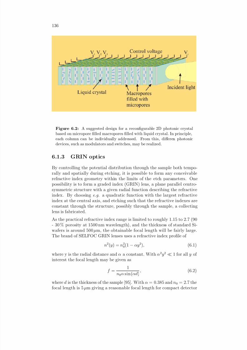
8/12/2019 Graded Optical Filters
http://slidepdf.com/reader/full/graded-optical-filters 146/164
136
Figure 6.2: A suggested design for a reconfigurable 2D photonic crystalbased on micropore filled macropores filled with liquid crystal. In principle,each column can be individually addressed. From this, differen photonicdevices, such as modulators and switches, may be realized.
6.1.3 GRIN optics
By controlling the potential distribution through the sample both tempo-rally and spatially during etching, it is possible to form any conceivablerefractive index geometry within the limits of the etch parameters. Onepossibility is to form a graded index (GRIN) lens, a plane parallel centro-symmetric structure with a given radial function describing the refractiveindex. By choosing e.g. a quadratic function with the largest refractiveindex at the central axis, and etching such that the refractive indexes areconstant through the structure, possibly through the sample, a collectinglens is fabricated.
As the practical refractive index range is limited to roughly 1.15 to 2.7 (90
- 30 % porosity at 1500 nm wavelength), and the thickness of standard Si-wafers is around 500 µm, the obtainable focal length will be fairly large.The brand of SELFOC GRIN lenses uses a refractive index profile of
n2(y) = n20(1 − αy2), (6.1)
where y is the radial distance and α a constant. With α2y2 1 for all y of interest the focal length may be given as
f = 1
n0α sin(αd), (6.2)
where d is the thickness of the sample [95]. With α = 0.385 and n0 = 2.7 thefocal length is 5 µm giving a reasonable focal length for compact detector

8/12/2019 Graded Optical Filters
http://slidepdf.com/reader/full/graded-optical-filters 147/164
137
applications. The circular lens would then be etched through the sampleand have a refractive index along the central axis of 2.7 decreasing out tothe rim to 1.15 at a radius of about 2.5 mm.
The GRIN design may also be used for waveguiding, as is the case for acertain type of optical fiber. One challenging element of combining micro-technology and optics, usually referred to as micro photonics, is the cou-pling of light from the transportation level (fiber) to the manipulation level(chip/device). Aligning fibers to waveguides on an optical integrated cir-cuit (OIC) is difficult as the areas to be aligned have a typical size in theµm range. One way of doing this which has proven quite efficient has beento etch grooves adjacent to the waveguide-entrance during processing of the OIC. The fiber will then be centered upon placement and fastening.However, there will be a substantial loss of signal as there will most likely
be an air gap between the fiber-end and the waveguide-entrance. Thismethod is also permanent. One potential application where the couplingof light and OICs is non-permanent is in the processing of lab-on-a-chips.In this case a specially designed chip may manipulate a physical sample,e.g. liquid containing DNA, through heat treatment and transport throughmicro-conduits. The measurement of parameters of interest may be done byluminescense measurements at some position on the lab-on-a-chip with anexternal excitation source and detector. By integrating some of the optics,e.g. waveguides, it may be possible to measure more parameters and makethe measurement more selective or sensitive. To make a non-permanent,
robust coupling between a fiber and an optical circuit the GRIN propertiesof PS may be utilized. It is also possible to integrate the light sources withthe lab-on-a-chip also, possibly PS LEDs or nanodot LEDs/lasers. In thiscase the system will be even more compact and coupling to and from thechip is avoided.
Waveguides fabricated with PS have been reported by Loni [96] and oth-ers [97, 98, 99]. By combining a standard waveguide with a specially de-signed coupling area, a good coupling with little loss may be possible. Aschematic of the idea is shown in Fig. 6.3. Guiding of light is most oftenbased on total internal reflection which is possible when light in a medium
is reflected off an interface to another medium with a lower refractive indexat a minimum angle. This is shown in Fig. 6.3 as a darkly colored guid-ing core (high index) surrounded by a lighter colored cladding layer (lowindex). However, to minimize back-reflectance from the air-guide interfacethe guide refractive index should match as well as possible the air refrac-tive index. These conflicting requirements may be resolved by graduallyincreasing the core index from the coupling area at the surface to the guide.The curvature of the core in the coupling area should be small as this willreduce the loss due to non-total internal reflection conditions close to thesurface - the core has a lower index than the cladding here. This design
seems quite robust in that there is a range of acceptable angles and thereare no movable parts.

8/12/2019 Graded Optical Filters
http://slidepdf.com/reader/full/graded-optical-filters 148/164
138
Figure 6.3: A fiber-to-chip optical coupler using graded index PS areas. Agraded refractive index area is used to minimize back reflectance and steerthe beam into the waveguide. The waveguide may also consist of PS, bothhigh and low porosity.
6.1.4 Novel optical filter
An interesting use of PS graded index filters is in anti-reflection coatings(ARC) for crystalline Si solar cells [100]. Graded index ARCs have the po-tential of being very broad band and work at a wide range of angles [101].However, these qualities typically come at the expense of greater filter thick-ness. The thickness of the ARC is crucial when used in conjunction withsolar cells, as the the efficiency of the cell depends on photon absorption inthe correct location in the cell. With a thicker ARC, more absorption willtake place in the filter itself which does not generate any photo-current. Abalance may be found between the angular range for which the ARC givesgood results and the thickness in such a way that the cell proves overall
more efficient for a wide range of positions relative to the sun. With animmovable cell, the daily energy conversion increases due to more efficientconversion when the sun is at the horizon.
For both the ARC and the waveguide-optical filter coupler it would be ben-eficial if the lowest refractive index of the PS would be lowered further,while at the same time increasing the gradient such that the highest refrac-tive index is kept constant. This may be done by gradually oxidizing thePS. The relative change in refractive index would be higher where more of the total volume of Si in the PS is oxidized, as would happen in the highporosity regions. By choosing the right oxidation conditions, the outermost
part of the PS, in a graded index layer, would be fully oxidized resulting inporous SiO2 while the innermost would be, relative to volume, much less

8/12/2019 Graded Optical Filters
http://slidepdf.com/reader/full/graded-optical-filters 149/164
139
oxidized.
6.2 MOEMS devices
Enabling optical elements, like filters, to move on a chip level opens up vastpossibilities within practical applications.
6.2.1 Membrane based MEMS pressure sensors
It has become nearly a standard to measure movement of elements ina micro-electro-mechanical-system (MEMS) by resistivity changes in dif-
fused/deposited piezoresistors at critical points. An alternative to this couldbe to use PS optical filters.
Membrane based pressure sensors in MEMS technology often uses piezore-sistors to measure the strain in the membrane as the pressure increases.By etching a PS filter with a narrow reflection band on the membrane, thestretching due to the strain could possibly expand the pores thus decreasingthe refractive index and shifting the reflectance band center wavelength. Asuitable structure for this could be a rugate filter. A sketch of a possibledesign is shown in Fig. 6.4a. This effect has not yet been measured and itis not known if a change in refractive index would be significant in such a
system.
Considering that with a proper design, a change in porosity of 0.04 % (abs.)may result in a shift in the reflection band of 1 nm, it should be possibleto measure small, strain induced changes in porosity. This is based on athick Bragg reflector for reflectance at 1550 nm. A rough model may beused to get a feel for the strain induced porosity change; consider a 100 µmdiameter membrane used as a pressure sensor. This membrane may havea maximum vertical deflection in the order of 100 nm. This results in astretching of the membrane surface of a few percent (< 10 %). Describingthe porous silicon as consisting of disconnected pillars of silicon with airbetween, a 1 % increase in the distance between columns in both lateraldirections would lead to a porosity change in the order of 0.1 %, hence, thestrain induced porosity change could be measurable.
One could make use of this effect in a pressure sensor by using a hybridstructure where a broad band light source and a spectrometric sensor isintegrated to measure the spectral shift of the reflection band from thedeflected and stretched membrane.
Another alternative pressure sensor could be one based on interferencewhere the membrane functions as one of two mirrors in a Fabry-Perot filter
and an inflexible substrate is bonded on top of the membrane forming anarrow cavity between. To increase sensitivity either or both of the sides

8/12/2019 Graded Optical Filters
http://slidepdf.com/reader/full/graded-optical-filters 150/164
140
of the cavity may be etched to form a PS reflectance filter. With a higherreflection from the mirrors on both sides of the cavity, the cavity modewill be sharper, hence smaller shifts in the cavity mode due to membrane
movement may be detected. A sketch showing the principle of the deviceis shown in Fig. 6.4b. This type of pressure sensor is being used today asmicrophones because of the quick response and high sensitivity.
a) b)
Figure 6.4: a) A suggestion for a pressure sensor based on change in porositydue to strain in the membrane. A reflectance filter structure is etched in PSon the membrane. This will stretch and shift the reflectance band of thefilter when pressure exerts a force on the membrane. b) The principle of a Fabry-Perot microphone with PS reflectors on both sides of the cavity.This could increase the sensitivity of the device. Acoustic waves deflect themembrane, changing the resonance frequency and decreases the intensity of a monochromatic beam. The transmitted beam intensity is detected with apn-junction in the substrate below the cavity.
6.2.2 MOEMS optical scanner and switch
By using a comb drive as shown schematically in Fig. 6.5, a filter may bemoved back and forth in the plane with a quick response rate. This device
may be used in several different ways. With a broad band light sourcedirected at a graded narrow band reflectance filter the device may be usedas a scanning ”monochromatic” light-source with the output light being of a selectable wavelength. A similar device has been reported by Lammel et
al. [102], however, this was an upright filter where the filter angle could bevaried.
The known light source may be exchanged by an unknown, external lightsource to be analyzed. A detector may then be placed in the path of the lightat the output. By then scanning the graded narrow band filter, the detectoroutput will be proportional to the intensity of the wavelength reflected from
the filter giving the spectral content of the source. An extension to thiswould be to place a line array of detectors at the output, with the positioning

8/12/2019 Graded Optical Filters
http://slidepdf.com/reader/full/graded-optical-filters 151/164
141
of the array such that the length is perpendicular to scan direction and thelength of the array similar to the width of the filter, hence quite a wide filterwould be necessary. This would increase the inertial mass and reaction time
suggesting that perhaps several filters in parallel could be used. This setupwould enable a multispectral line array detector which could be used for,e.g., spatially resolved gas detection or environmental monitoring.
Instead of a graded filter it is possible to make binary filters such as reportedby Arens-Fischer et al. [103]. By fabricating an ARC on one end of the filterand a reflection filter on the other end a switch may be realized. The inputbeam to be switched on or off may be provided by fiber, and the outputbeam may be coupled to a fiber. This setup should give a very high signalon/off ratio. The switching rate of such a device should be in the singledigit to double digit kHz following the resonance frequency of reported
comb drive devices [104]. This is not high enough for data package routingin telecom networks, but should be enough for network reconfiguration andperhaps other applications.
Figure 6.5: A MOEMS device making use of a graded PS filter. This basicelement may be used in several different applications. The filter element iscoupled to a system of comb-drives which is able to horizontally translate
the filter. One application as suggested in the figure is an imaging spectralscanner.
6.2.3 Multispectral MOEMS pixel array
A somewhat more complex detector based on the same technique as above,is an array of diode detectors in plane with movable graded narrow bandtransmission filters on top of each. This would give the sensor array mul-tispectral detection capability. The filters will have an optimized gradient
and bandwidth depending on the demands for sensitivity or detection range.The processing of this device would necessarily be quite complex and the fill

8/12/2019 Graded Optical Filters
http://slidepdf.com/reader/full/graded-optical-filters 152/164
142
factor quite low as it would be necessary to have quite long filters comparedto the size of the detector for a practical measurable spectral range. Thebenefits would be a very fast, compact and monolithic imaging multispec-
tral detector.
6.2.4 Holographic scanner
The PS multilayer etching technique introduced by Volk et al. [28] may beused to produce holographic diffraction gratings, i.e. gratings with sinu-soidal groove profile. This has a potential for many different applications.The grating fabrication is based on the formation of n-doped regions be-neath p-doped regions in p-type Si and deposition of an insulating and HF
resistant Si3N4 layer on the surface with openings above the n-doped regionsso that current is forced to run parallel with the surface above the n-dopedregions. Grooves in the Si are etched at the openings of the nitride layerdown to the n-region so that the etching occurs from a vertical surface witha lateral homogeneous current density. By then etching as described earlierin this thesis, one may obtain horizontal multilayers. By then removingthe nitride layer one may use this as an amplitude grating as the different”grooves” (layer cross-sections) have different reflection coefficients due todifferent refractive indexes. By etching lightly in a porosity selective alka-line etch, e.g. KOH, one would form proper grooves fabricating a phasegrating. It would be possible to form a holographic grating by etching
a rugate porosity profile with the subsequent alkaline etch improving thediffraction properties of the grating.
This grating could be formed and released such that it would be connectedto a comb drive as explained above, similar to Fig. 6.5. By changing therugate period (or discrete repetition rate) during etching in a continuousfashion the diffraction properties would change with position. The zerothdiffraction order will always be present in the output from the grating, andit will have the same angle as the input beam independent of grating param-eters, however, the angle of the other orders depend on several parameters,such as grating period. By focusing on the -1st order, a system may bedesigned that has as an input a monochromatic laser beam at a set angleand as output the zeroth order beam which may be attenuated, and a -1storder beam which changes angle with the lateral position of the gratingdue to different grating periods. The standard diffraction equation givesan estimate of the relationship between incident angle, output angles fordifferent diffraction orders, wavelength and grating period:
sin α + sin β m = −mλ/d. (6.3)
A rough estimate of a possible design is as follows: the diffracted beam
of order m=-1 will change the output angle, β −1, from about -5
to 5
with a change in period, d, from 570 to 680 nm at a wavelength λ=600nm

8/12/2019 Graded Optical Filters
http://slidepdf.com/reader/full/graded-optical-filters 153/164
143
with the incident angle, α, being 75. Assuming the beam to be scannedis a monochromatic laser beam of diameter 50 µm and that the change of grating period within one diameter is 20 nm (roughly 2 output difference
between maximum and minimum diffraction period within the beam) theneeded scan length would be about 250 µm. This may result in a fairlyquick and compact laser scanner. A schematic drawing showing the gradedgrating is shown in Fig. 6.6.
Figure 6.6: The shown grating consists of a laterally etched PS multilayerstructure with a grading in layer period. In this case a lying down Braggreflector is shown. A holographic grating could be obtained with a lyingdown rugate reflector. The surface structure is obtained by lightly etchingin, e.g., KOH which will etch highly porous silicon faster than silicon of lowerporosity. The diffracted beams of order=0 will change angle depending onthe diffraction period where the incident beam hits.

8/12/2019 Graded Optical Filters
http://slidepdf.com/reader/full/graded-optical-filters 154/164

8/12/2019 Graded Optical Filters
http://slidepdf.com/reader/full/graded-optical-filters 155/164
Chapter 7
Conclusion
In this thesis a method for the in situ monitoring of parameters criticalfor optical applications during etching of porous silicon has been described.Data obtained by this method has been used to fabricate different types of interference based optical filters in porous silicon.
The development of the method for in situ monitoring includes the develop-ment of a optical fiber based measurement system composed of an infraredlaser coupled to the dry side of the Si-sample in the etch cell during etch-ing and a detector to measure the intensity of the reflected beam. As thesystem is fiber based, it is compact and the system hardware may be ata distance from any harmful chemicals. The reflected beam contains anoscillating signal due to interference between the beams partially reflectedoff the different interfaces in the porous silicon sample; front side, poroussilicon–substrate interface and back side. By analyzing the reflected in-terference signal with a short-time Fourier transform, the instantaneous ordepth dependent porosity is obtained along with the instantaneous or depthdependent etch rate and porous silicon–substrate interface roughness.
Information on porosity and etch rate from both gravimetrical measure-ments as well as the in situ reflectance method has been used to etch both
discrete and inhomogeneous (rugate) optical interference filters in the visi-ble and near-infrared spectral range. By applying a voltage laterally acrossthe Si-samples during porous silicon filter fabrication, the resulting filtershad a gradient in the filter response in the direction of the voltage drop.This could be developed into a near-infrared spectrometer.
The porosities and etch rates obtained by the in situ reflectance methodshow a very strong dependence on etch time. This affects the filter etchingsuch that the resulting filter response is non-optimal. Attempts at coun-teracting this time variation is shown. A discussion of the causes of thenon-optimality of the filter responses is given as well as possible ways of
avoiding the detrimental effects of this time variation which is importantfor fabricating infrared optical filters of very good quality.
145

8/12/2019 Graded Optical Filters
http://slidepdf.com/reader/full/graded-optical-filters 156/164
146
Possible uses of porous silicon in other novel applications, both passive andin conjunction with micro-opto-electro-mechanical-systems are discussed inthe last chapter.

8/12/2019 Graded Optical Filters
http://slidepdf.com/reader/full/graded-optical-filters 157/164
Bibliography
[1] O. Boyraz and B. Jalali. Demonstration of a silicon raman laser. Opt.
Express , 12(21):5269, 2004.
[2] H. S. Rong, A. S. Liu, R. Jones, O. Cohen, D. Hak, R. Nicolaescu,A. Fang, and M. Paniccia. An all-silicon raman laser. Nature ,433(7023):292, 2005.
[3] A. Irace, G. Breglio, M. Iodice, and A. Cutolo. Light modulation withsilicon devices. In L Pavesi and Dj Lockwood, editors, Silicon Photon-
ics , volume 94 of Topics in Applied Physics , page 361. Springer-VerlagGmbH, 2004.
[4] A. Uhlir. Electrolytic shaping of germanium and silicon. Bell Syst.
Tech. J., 35(2):333, 1956.
[5] D. R. Turner. Electropolishing silicon in hydrofluoric acid solutions.J. Electrochem. Soc., 105(7):402, 1958.
[6] Y. Watanabe and T. Sakai. Application of a thick anode film tosemiconductor devices. Rev. Elec. Commun. Lab., 19(7-8):899, 1971.
[7] M. J. J. Theunissen. Etch channel formation during anodic dissolutionof n-type silicon in aqueous hydrofluoric acid. J. Electrochem. Soc.,119(3):351, 1972.
[8] Y. Watanabe, Y. Arita, T. Yokoyama, and Y. Igarashi. Formationand properties of porous silicon and its application. J. Electrochem.
Soc., 122(10):1351, 1975.
[9] T. Unagami. Oxidation of porous silicon and properties of its oxidefilm. Jpn. J. Appl. Phys., 19(2):231, 1980.
[10] L. T. Canham. Silicon quantum wire array fabrication by electrochem-ical and chemical dissolution of wafers. Appl. Phys. Lett., 57(10):1046,1990.
[11] N. Koshida and H. Koyama. Visible electroluminescence from poroussilicon. Appl. Phys. Lett., 60(3):347, 1992.
147

8/12/2019 Graded Optical Filters
http://slidepdf.com/reader/full/graded-optical-filters 158/164
148
[12] O. Bisi, S. Ossicini, and L. Pavesi. Porous silicon: A quantum spongestructure for silicon based optoelectronics. Surf. Sci. Rep., 38(1-3):5,2000.
[13] M. I. J. Beale, J. D. Benjamin, M. J. Uren, N. G. Chew, and A. G.Cullis. An experimental and theoretical-study of the formation andmicrostructure of porous silicon. J. Cryst. Growth , 73(3):622, 1985.
[14] C. Pickering, M. I. J. Beale, D. J. Robbins, P. J. Pearson, andR. Greef. Optical-properties of porous silicon films. Thin Solid Films ,125(1-2):157, 1985.
[15] G. Vincent. Optical-properties of porous silicon superlattices. Appl.
Phys. Lett., 64(18):2367, 1994.
[16] M. G. Berger, C. Dieker, M. Thonissen, L. Vescan, H. Luth,H. Munder, W. Theiß, M. Wernke, and P. Grosse. Porosity super-lattices - a new class of si heterostructures. J. Phys. D Appl. Phys.,27(6):1333, 1994.
[17] C. Mazzoleni and L. Pavesi. Application to optical-components of dielectric porous silicon multilayers. Appl. Phys. Lett., 67(20):2983,1995.
[18] L. Pavesi, C. Mazzoleni, A. Tredicucci, and V. Pellegrini. Controlled
photon-emission in porous silicon microcavities. Appl. Phys. Lett.,67(22):3280, 1995.
[19] Y. Zhou, P. A. Snow, and P. S. J. Russell. Strong modification of pho-toluminescence in erbium-doped porous silicon microcavities. Appl.
Phys. Lett., 77(16):2440, 2000.
[20] M. Thonissen, M. Marso, R. Arens-Fischer, D. Hunkel, M. Kruger,V. Ganse, H. Luth, and W. Theiß. Electrical control of the reflectanceof porous silicon layers. J. Porous Mat., 7(1-3):205, 2000.
[21] M. V. Wolkin, S. Chan, and P. M. Fauchet. Porous silicon encap-sulated nematic liquid crystals for electro-optic applications. Phys.
Stat. Sol. a , 182(1):573, 2000.
[22] S. M. Weiss and P. M. Fauchet. Electrically tunable porous siliconactive mirrors. Phys. Stat. Sol. a , 197(2):556, 2003.
[23] S. Weiss, M. Molinari, and P. Fauchet. Temperature stabilityfor silicon-based photonic band-gap structures. Appl. Phys. Lett.,83(10):1980, 2003.
[24] J. Diener, N. Kunzer, E. Gross, D. Kovalev, and M. Fujii. Planarsilicon-based light polarizers. Opt. Lett., 29(2):195, 2004.

8/12/2019 Graded Optical Filters
http://slidepdf.com/reader/full/graded-optical-filters 159/164
149
[25] M. Thust, M. J. Schoning, S. Frohnhoff, R. Arens-Fischer, P. Kordos,and H. Luth. Porous silicon as a substrate material for potentiometricbiosensors. Meas. Sci Technol., 7(1):26, 1996.
[26] V. S. Y. Lin, K. Motesharei, K. P. S. Dancil, M. J. Sailor, and M. R.Ghadiri. A porous silicon-based optical interferometric biosensor. Sci-
ence , 278(5339):840, 1997.
[27] G. Lerondel, R. Romestain, J. C. Vial, and M. Thonissen. Poroussilicon lateral superlattices. Appl. Phys. Lett., 71(2):196, 1997.
[28] J. Volk, N. Norbert, and I. Barsony. Laterally stacked porous siliconmultilayers for subquart micron period uv gratings. Phys. Stat. Sol.
a , 202(8):1707, 2005.
[29] E. Lorenzo-Cabrera, C. J. Oton, N. E. Capuj, M. Ghulinyan,D. Navarro-Urrios, Z. Gaburro, and L. Pavesi. Porous silicon-basedrugate filters. Appl. Opt., 2005.
[30] M. G. Berger, R. Arens-Fischer, M. Thonissen, M. Kruger, S. Billat,H. Luth, S. Hilbrich, W. Theiß, and P. Grosse. Dielectric filters madeof ps: Advanced performance by oxidation and new layer structures.Thin Solid Films , 297(1-2):237, 1997.
[31] J. L. Coffer. Porous silicon formation by stain etching. In L Canham,
editor, Properties of Porous Silicon , volume 18 of Emis Datareviews Series , page 223. INSPEC, IEE, London, United Kingdom, 1997.
[32] H. Foll, M. Christophersen, J. Carstensen, and G. Hasse. Formationand application of porous silicon. Mat. Sci. Eng. R, 39(4):93, 2002.
[33] X. G. Zhang. Morphology and formation mechanisms of porous sili-con. J. Electrochem. Soc., 151(1):C69, 2004.
[34] R. L. Smith and S. D. Collins. Porous silicon formation mechanisms.J. Appl. Phys., 71(8):R1, 1992.
[35] V. Lehmann and U. Gosele. Porous silicon formation - a quantumwire effect. Appl. Phys. Lett., 58(8):856, 1991.
[36] J. Carstensen, M. Christophersen, and H. Foll. Pore formation mech-anisms for the si-hf system. Mat. Sci. Eng. B-Solid , 69:23, 2000.
[37] V. Lehmann and S. Ronnebeck. The physics of macropore formationin low-doped p-type silicon. J. Electrochem. Soc., 146(8):2968, 1999.
[38] D. T. J. Hurle and P. Rudolph. A brief history of defect formation,
segregation, faceting, and twinning in melt-grown semiconductors. J.Cryst. Growth , 264(4):550, 2004.

8/12/2019 Graded Optical Filters
http://slidepdf.com/reader/full/graded-optical-filters 160/164
150
[39] G. Lerondel, R. Romestain, and S. Barret. Roughness of the poroussilicon dissolution interface. J. Appl. Phys., 81(9):6171, 1997.
[40] H. Topsøe. Geometric Factors in Four Point Resistivity Measurement .http://www.four-point-probes.com/haldor.html, 1968.
[41] G. Lerondel, P. Reece, A. Bruyant, and M. Gal. Strong light confine-ment in microporous photonic silicon structures. Materials Research
Society Symposium Proceeding , 797:W1.7.1, 2004.
[42] G. Lerondel, G. Amato, A. Parisini, and L. Boarino. Porous siliconnanocracking. Mat. Sci. Eng. B-Solid , 69:161, 2000.
[43] D. Bellet and L. T. Canham. Controlled drying: The key to betterquality porous semiconductors. Adv. Mater., 10(6):487, 1998.
[44] L. T. Canham, A. G. Cullis, C. Pickering, O. D. Dosser, T. I. Cox,and T. P. Lynch. Luminescent anodized silicon aerocrystal networksprepared by supercritical drying. Nature , 368(6467):133, 1994.
[45] L. Canham, editor. Properties of Porous Silicon , volume 18 of Emis
Datareviews Series . INSPEC, IEE, London, United Kingdom, 1997.
[46] J. Salonen, E. Laine, and L. Niinisto. Thermal carbonization of poroussilicon surface by acetylene. J. Appl. Phys., 91(1):456, 2002.
[47] S. Setzu, G. Lerondel, and R. Romestain. Temperature effect on theroughness of the formation interface of p-type porous silicon. J. Appl.
Phys., 84(6):3129, 1998.
[48] Crc Handbook of Chemistry and Physics . CRC Press, 78th edition,1998.
[49] Femlab, comsol, inc., burlington, massachusetts, usa, 2004.
[50] O. S. Heavens. Optical Properties of Thin Solid Films . Dover Clas-sics of Science and Mathematics. Dover Publications, Inc., New York,
1991.
[51] D. J. Bergman. Dielectric-constant of a composite-material - problemin classical physics. Phys. Rep., 43(9):378, 1978.
[52] J. C. Maxwell Garnett. Philos. Trans. R. Soc. London , 203:385, 1904.
[53] H. Looyenga. Dielectric constants of heterogeneous mixtures. Physica ,31(3):401, 1965.
[54] D. A. G. Bruggeman. Ann. Phys., 24:636, 1935.
[55] W. Theiß. Optical properties of porous silicon. Surf. Sci. Rep., 29(3-4):95, 1997.
8/12/2019 Graded Optical Filters
http://slidepdf.com/reader/full/graded-optical-filters 161/164
151
[56] W. Theiß and S. Hilbrich. Refractive index of porous silicon. InL Canham, editor, Properties of Porous Silicon , volume 18 of Emis
Datareviews Series , page 223. INSPEC, IEE, London, United King-
dom, 1997.
[57] D. E. Aspnes and J. B. Theeten. Investigation of effective-mediummodels of microscopic surface-roughness by spectroscopic ellipsome-try. Phys. Rev. B , 20(8):3292, 1979.
[58] E. K. Squire, P. A. Snow, P. S. Russell, L. T. Canham, A. J. Si-mons, and C. L. Reeves. Light emission from porous silicon singleand multiple cavities. J. Lumin., 80(1-4):125, 1998.
[59] P. J. Reece, G. Lerondel, W. H. Zheng, and M. Gal. Optical micro-
cavities with subnanometer linewidths based on porous silicon. Appl.Phys. Lett., 81(26):4895, 2002.
[60] J. R. Reitz, F. J. Milford, and R. W. Christy. Foundations of Electro-
magnetic Theory . Addison-Wesley Publishing Company, Inc., Read-ing, Massachusetts, USA, 4th edition, 1993.
[61] E. D. Palik. Handbook of Optical Constants of Solids . Academic,Orlando, FL, USA, 1985.
[62] P. A. Schumann, W. A. Keenan, A. H. Tong, G. H. H, and S. C. P.Silicon optical constants in infrared. J. Electrochem. Soc., 118(1):145,1971.
[63] M. Born and E. Wolf. Principles of Optics . University Press, Cam-bridge, UK, 7th edition, 1999.
[64] Z. Knittl. Optics of Thin Films . Wiley Series in Pure and AppliedOptics. Wiley, London, 1976.
[65] C. L. Mitsas and D. I. Siapkas. Generalized matrix-method for analy-
sis of coherent and incoherent reflectance and transmittance of multi-layer structures with rough surfaces, interfaces, and finite substrates.Appl. Opt., 34(10):1678, 1995.
[66] H. E. Bennett and J. O. Porteus. Relation between surface rough-ness and specular reflectance at normal incidence. J. Opt. Soc. Am.,51(2):123, 1961.
[67] H. Davies. The reflection of electromagnetic waves from a rough sur-face. P. I. Electr. Eng., 101(7):209, 1954.
[68] I. Filinski. Effects of sample imperfections on optical-spectra. Phys.Status Solidi B , 49(2):577, 1972.

8/12/2019 Graded Optical Filters
http://slidepdf.com/reader/full/graded-optical-filters 162/164
152
[69] M. Kildemo. Real-time monitoring and growth control of si-gradient-index structures by multiwavelength ellipsometry. Appl.
Opt., 37(1):113, 1998.
[70] H. Bartzsch, S. Lange, R. Frach, and K. Goedicke. Graded refrac-tive index layer systems for antireflective coatings and rugate filtersdeposited by reactive pulse magnetron sputtering. Surf. Coat. Tech.,180-81:616, 2004.
[71] A. V. Tikhonravov, M. K. Trubetskov, J. Hrdina, and J. Sobota.Characterization of quasi-rugate filters using ellipsometric measure-ments. Thin Solid Films , 277(1-2):83, 1996.
[72] K. Robbie, A. J. P. Hnatiw, M. J. Brett, R. I. Macdonald, and J. N.Mcmullin. Inhomogeneous thin film optical filters fabricated usingglancing angle deposition. Electron. Lett., 33(14):1213, 1997.
[73] K. Kaminska, T. Brown, G. Beydaghyan, and K. Robbie. Vacuumevaporated porous silicon photonic interference filters. Appl. Opt.,42(20):4212, 2003.
[74] W. J. Gunning, R. L. Hall, F. J. Woodberry, W. H. Southwell, andN. S. Gluck. Codeposition of continuous composition rugate filters.Appl. Opt., 28(14):2945, 1989.
[75] B. G. Bovard. Rugate filter theory - an overview. Appl. Opt.,
32(28):5427, 1993.
[76] W. H. Southwell and R. L. Hall. Rugate filter sidelobe suppres-sion using quintic and rugated quintic matching layers. Appl. Opt.,28(14):2949, 1989.
[77] W. H. Southwell. Extended-bandwidth reflector designs by usingwavelets. Appl. Opt., 36(1):314, 1997.
[78] A. C. Van Popta, M. M. Hawkeye, J. C. Sit, and M. J. Brett. Gradient-index narrow-bandpass filter fabricated with glancing-angle deposi-tion. Opt. Lett., 29(21):2545, 2004.
[79] A. Bruyant, G. Lerondel, P. J. Reece, and M. Gal. All-silicon omni-directional mirrors based on one-dimensional photonic crystals. Appl.
Phys. Lett., 82(19):3227, 2003.
[80] E. Steinsland, T. Finstad, and A. Hanneborg. Laser reflectance in-terferometry for in situ determination of silicon etch rate in varioussolutions. J. Electrochem. Soc., 146(10):3890, 1999.
[81] M. Thonissen, M. G. Berger, S. Billat, R. Arens-Fischer, M. Kruger,H. Luth, W. Theiß, S. Hillbrich, P. Grosse, G. Lerondel, and
U. Frotscher. Analysis of the depth homogeneity of p-ps by reflectancemeasurements. Thin Solid Films , 297(1-2):92, 1997.
8/12/2019 Graded Optical Filters
http://slidepdf.com/reader/full/graded-optical-filters 163/164
153
[82] Z. Gaburro, C. J. Oton, P. Bettotti, L. Dal Negro, G. V. Prakash,M. Cazzanelli, and L. Pavesi. Interferometric method for moni-toring electrochemical etching of thin films. J. Electrochem. Soc.,
150(6):C381, 2003.
[83] D. Navarro-Urrios, C. Perez-Padrn, E. Lorenzo, N. E. Capuj,Z. Gaburro, C. J. Oton, and L. Pavesi. Chemical etching effects inporous silicon layers. Proc. SPIE , 5118:109, 2003.
[84] T. Unagami. Intrinsic stress in porous silicon layers formed by an-odization in hf solution. J. Electrochem. Soc., 144(5):1835, 1997.
[85] M. Thonissen, S. Billat, M. Kruger, H. Luth, M. G. Berger,U. Frotscher, and U. Rossow. Depth inhomogeneity of porous sili-
con layers. J. Appl. Phys., 80(5):2990, 1996.[86] M. Thonissen and M. G. Berger. Multilayer structures of porous
silicon. In L Canham, editor, Properties of Porous Silicon , volume 18of Emis Datareviews Series , page 30. INSPEC, IEE, London, UnitedKingdom, 1997.
[87] S. Billat, M. Thonissen, R. Arens-Fischer, M. G. Berger, M. Kruger,and H. Luth. Influence of etch stops on the microstructure of poroussilicon layers. Thin Solid Films , 297(1-2):22, 1997.
[88] M. Thonissen. Spektoskopische Charakterisierung Von Schichten Und
Schichtsystemen Aus Por¨ osem Silicium Im Hinblick Auf Optische
Und Optoelektronische Anwendungen . PhD thesis, Forschungszen-trum Julich, 1999.
[89] G. Lammel. New Micromachining Technologies Using Porous Silicon .Phd thesis, Swiss Federal Institute of Technology, 2001.
[90] M. C. Li, L. C. Zhao, and X. K. Chen. Reducing the effective barrierheight of a ptsi schottky diode by a p+ doping spike using pulsed laserdoping. J. Phys. D Appl. Phys., 36:2347, 2003.
[91] F. Raissi and M. M. Far. Highly sensitive ptsi/porous si schottkydetectors. IEEE Sens. J., 2(3):476, 2002.
[92] G. Parker and M. Charlton. Photonic crystals. Phys. World , 13(8):29,2000.
[93] F. Muller, A. Birner, U. Gosele, V. Lehmann, S. Ottow, and H. Foll.Structuring of macroporous silicon for applications as photonic crys-tals. J. Porous Mat., 7(1-3):201, 2000.
[94] D. Hamm, T. Sakka, and Y. Ogata. Porous silicon formation under
constant anodization conditions: Homogeneous regime or transition?J. Electrochem. Soc., 151(1):C32, 2004.

8/12/2019 Graded Optical Filters
http://slidepdf.com/reader/full/graded-optical-filters 164/164
154
[95] B. E. A. Saleh and M. C. Teich. Fundamentals of Photonics . WileySeries in Pure and Applied Optics. John Wiley & Sons, Inc., NewYork, NY, USA, 1991.
[96] A. Loni, L. T. Canham, M. G. Berger, R. Arens-Fischer, H. Munder,H. Luth, H. F. Arrand, and T. M. Benson. Porous silicon multilayeroptical waveguides. Thin Solid Films , 276(1-2):143, 1996.
[97] M. Araki, H. Koyama, and N. Koshida. Fabrication and fundamentalproperties of an edge-emitting device with step-index porous siliconwaveguide. Appl. Phys. Lett., 68(21):2999, 1996.
[98] T. M. Benson, H. F. Arrand, P. Sewell, D. Niemeyer, A. Loni,R. J. Bozeat, M. Kruger, R. Arens-Fischer, M. Thonissen, and
H. Luth. Progress towards achieving integrated circuit functional-ity using porous silicon optoelectronic components. Mat. Sci. Eng.
B-Solid , 69:92, 2000.
[99] P. Ferrand and R. Romestain. Optical losses in porous silicon waveg-uides in the near-infrared: Effects of scattering. Appl. Phys. Lett.,77(22):3535, 2000.
[100] C. C. Striemer and P. M. Fauchet. Dynamic etching of silicon forbroadband antireflection applications Appl Phys Lett 81(16):2980


![[H.a. Macleod] Thin-Film Optical Filters](https://img.pdfslide.net/doc/110x75/553ff9e8550346096e8b4989/ha-macleod-thin-film-optical-filters.jpg)