Embed Size (px)
Citation preview
Appl Phys A (2012) 107:379–383DOI 10.1007/s00339-012-6806-9
Grain size effect on the giant dielectric and nonlinear electricalbehaviors of Bi1/2Na1/2Cu3Ti4O12 ceramics
Yang Qiu · Songliu Yuan · Zhaoming Tian ·Liang Chen · Chuanhui Wang · Hanning Duan ·Kai Guo
Received: 28 July 2011 / Accepted: 14 December 2011 / Published online: 23 February 2012© Springer-Verlag 2012
Abstract Single phase Bi1/2Na1/2Cu3Ti4O12 (BNCTO) ce-ramics with different grain sizes (1.4–4.3 µm) are preparedby a modified Pechini method to investigate their giant di-electric and nonlinear electrical behaviors. The results showthat the giant dielectric and nonlinear electrical behaviorsare strongly dependent on grain size. With the increment ofgrain size, the dielectric constant increases monotonicallyfrom 14110 (for 1.4 µm sample) to 36183 (for 4.3 µm sam-ple) at 1 kHz, in accompaniment with the breakdown voltagereducing from 112.5 to 43.2 V/mm and the nonlinear coef-ficient reducing from 4.9 to 3.4. On the basis of the internalbarrier layer capacitor (IBLC) model and the IBLC model ofSchottky-type potential barrier, an interpretation of the grainsize effect on the giant dielectric and nonlinear electrical be-haviors is presented.
1 Introduction
With the integration and miniaturization of electronic de-vices, multifunctional materials have attracted consider-able attention due to their potential applications. Recently,many perovskite-like oxides ACu3Ti4O12 (A = Ca, La2/3,Bi1/2Na1/2, etc.) with body-centered cubic crystal structure,have drawn considerable theoretical and experimental stud-ies [1–5]. Among them, CaCu3Ti4O12 (CCTO) is mostlystudied for its exceptional behavior. The static dielectric
Y. Qiu · S. Yuan (�) · Z. Tian · L. Chen · C. Wang · H. Duan ·K. GuoSchool of Physics, Huazhong University of Science andTechnology, Wuhan 430074, P.R. Chinae-mail: [email protected]
L. Chene-mail: [email protected]
constant of CCTO is about 104 around radio frequency atroom temperature, which is also thermal stable between 100and 600 K [1–3]. A different effect, the nonlinear electricalbehavior of pure and doped CCTO, has also been studied bymany researchers [6–10].
As for the origin of the giant dielectric property of CCTOand related ACu3Ti4O12 compounds, it is not fully under-stood up until now. A largest amount of investigations havebeen done to interpret the giant dielectric behavior [1–3, 11–15, 17]. Among all the models to explain the giant dielectricbehavior, the internal barrier layer capacitor (IBLC) model[11–14] is widely accepted. The giant dielectric behavior ofCCTO is strongly dependent on the microstructure (such asgrain size, sample density, thickness, etc.) and thermal pro-cessing conditions (sintering atmosphere, annealing temper-ature, etc.) [6–10, 14, 17, 20]. According to IBLC model,CCTO ceramics are electrically heterogeneous, consistingof n-type semiconductive grains and insulating grain bound-aries [13, 14]. To explain the origin of the electrically inho-mogeneous microstructure, two representative explanationshave been proposed. One involves the oxygen-loss from thelattice at high temperatures and the reoxidation of the grainboundaries during the cooling process [13, 14]. The otheris based on the oxidation-reduction reactions of Cu and Tiions during the heating and cooling process of synthesizingCCTO [15]. Due to the special microstructure, the Schottky-type electrostatic barrier forms at the grain boundary re-gions, which contributes to the nonlinear electrical behav-ior [7, 16]. In 2006, Ferrarelli et al. [4] reported the intrinsicpermittivity of Bi1/2Na1/2Cu3Ti4O12 (BNCTO) of ∼250 at10 K is much higher compared to ∼110 for CCTO. How-ever, the nonlinear electrical behavior of BNCTO has notbeen investigated up to now. Since the nonlinear electricalbehavior is favorable to analyze the formation mechanismsof the giant dielectric effect, it is necessary to study the non-
380 Y. Qiu et al.
linear electrical behavior of BNCTO to get a comprehensiveunderstanding of the giant dielectric effect.
In this work, BNCTO ceramics with different grain sizesare synthesized, and the effect of grain size on the giant di-electric and nonlinear electrical behaviors is investigated.The giant dielectric and nonlinear electrical behaviors areexplained by the internal barrier layer capacitor (IBLC)model and the IBLC model of Schottky-type potential bar-rier.
2 Experimental procedure
Polycrystalline BNCTO ceramics were prepared by a mod-ified Pechini method using bismuth nitrate (Bi(NO3)3·5H2O), natrium nitrate (NaNO3), copper (II) nitrate(Cu(NO3)2·3H2O), tetrabutyl titanate (IV) (C16H36O4Ti),citric acid (C6H8O7), and distilled water as raw materi-als. First, bismuth nitrate, natrium nitrate, copper (II) ni-trate, and tetrabutyl titanate (IV) were dissolved in dis-tilled water stoichiometrically according to the formula ofBi1/2Na1/2Cu3Ti4O12. Citric acid in 2:1 molar ratio with re-spect to the metallic cations was added to the solution asa chelator, and the solution was adjusted to a PH value of6.5∼7.5 by adding ammonia. Secondly, the mixture wasdried at 120°C to form xerogel, and then the obtained xe-rogel was milled for 2 h. After that, the precursory powderswere cold-pressed into pellets of 1 mm thickness and 12 mmdiameters. Finally, the pellets were sintered at 1000°C for2 h, 5 h, 10 h, and 20 h, respectively. Silver electrodes werecoated on both sides of the specimens for electrical mea-surements.
The temperature of possible decomposition and crystal-lization was determined by the thermogravimetric-differen-tial thermal analysis (TG-DTA) (Diamond, PerkinElmer In-strument, USA). The crystal structure and morphology ofthe samples were investigated by X-ray diffraction (X’PertPRO, PANalytical B.V, Holland) and field emission scan-ning electron microscopy (JSM 6700F, JEOL, Japan). Thedielectric properties of the ceramics were obtained with aprecision impedance analyzer (6500B, WK, UK) with anapplied AC voltage of 500 mV. The current–voltage (I–V )characteristics of the samples were studied using a Keithley2400 Source meter.
3 Results and discussions
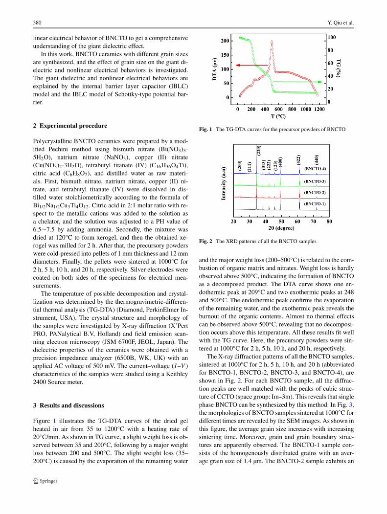
Figure 1 illustrates the TG-DTA curves of the dried gelheated in air from 35 to 1200°C with a heating rate of20°C/min. As shown in TG curve, a slight weight loss is ob-served between 35 and 200°C, following by a major weightloss between 200 and 500°C. The slight weight loss (35–200°C) is caused by the evaporation of the remaining water
Fig. 1 The TG-DTA curves for the precursor powders of BNCTO
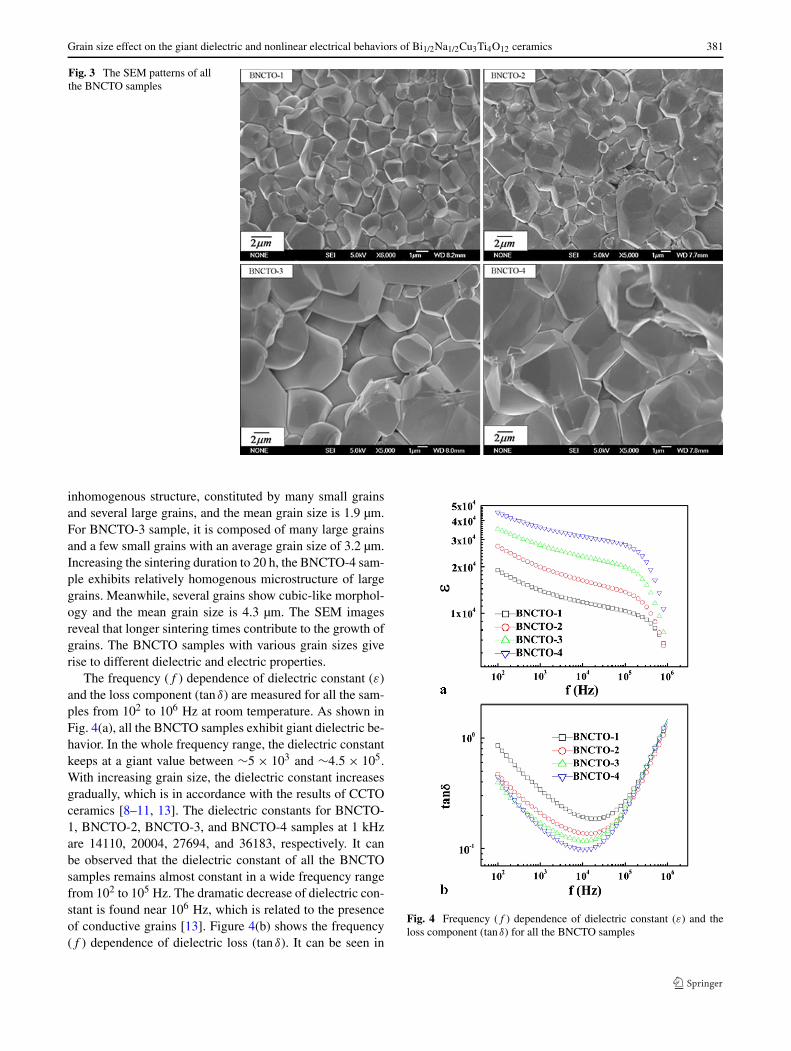
Fig. 2 The XRD patterns of all the BNCTO samples
and the major weight loss (200–500°C) is related to the com-bustion of organic matrix and nitrates. Weight loss is hardlyobserved above 500°C, indicating the formation of BNCTOas a decomposed product. The DTA curve shows one en-dothermic peak at 209°C and two exothermic peaks at 248and 500°C. The endothermic peak confirms the evaporationof the remaining water, and the exothermic peak reveals theburnout of the organic contents. Almost no thermal effectscan be observed above 500°C, revealing that no decomposi-tion occurs above this temperature. All these results fit wellwith the TG curve. Here, the precursory powders were sin-tered at 1000°C for 2 h, 5 h, 10 h, and 20 h, respectively.
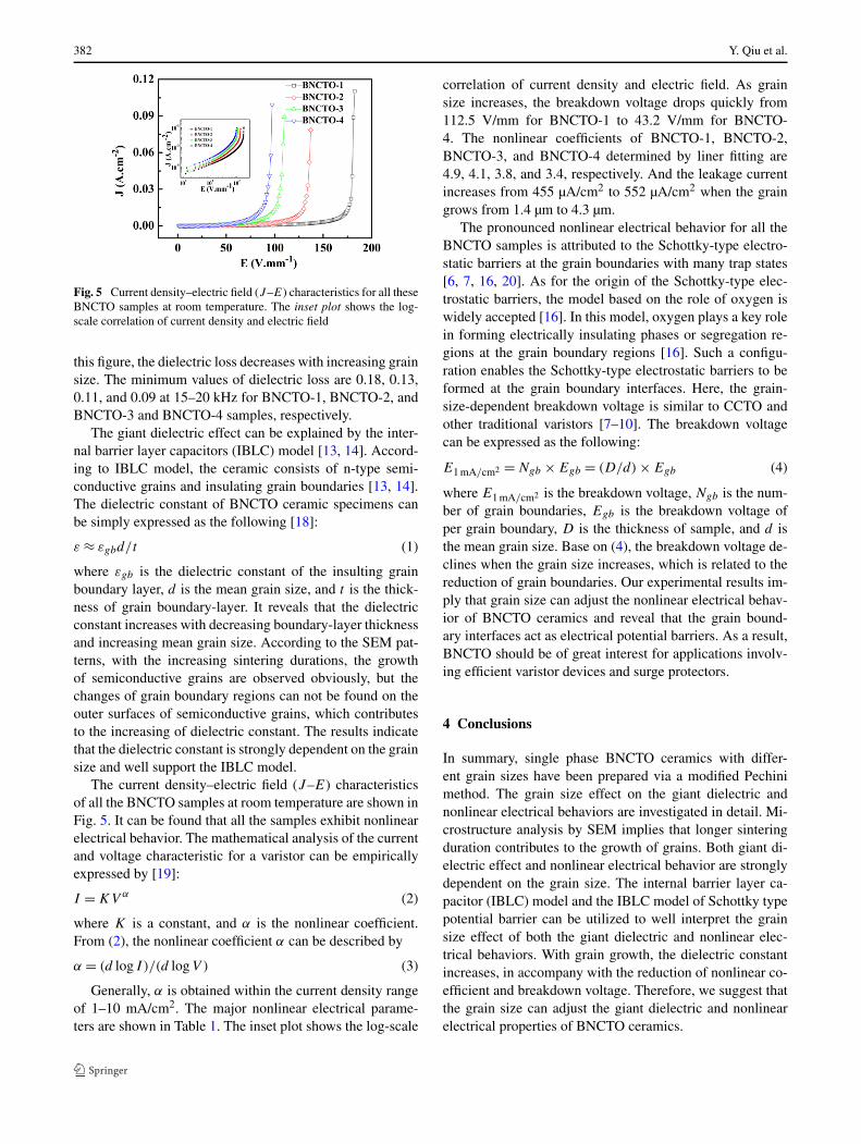
The X-ray diffraction patterns of all the BNCTO samples,sintered at 1000°C for 2 h, 5 h, 10 h, and 20 h (abbreviatedfor BNCTO-1, BNCTO-2, BNCTO-3, and BNCTO-4), areshown in Fig. 2. For each BNCTO sample, all the diffrac-tion peaks are well matched with the peaks of cubic struc-ture of CCTO (space group: Im–3m). This reveals that singlephase BNCTO can be synthesized by this method. In Fig. 3,the morphologies of BNCTO samples sintered at 1000°C fordifferent times are revealed by the SEM images. As shown inthis figure, the average grain size increases with increasingsintering time. Moreover, grain and grain boundary struc-tures are apparently observed. The BNCTO-1 sample con-sists of the homogenously distributed grains with an aver-age grain size of 1.4 µm. The BNCTO-2 sample exhibits an
Grain size effect on the giant dielectric and nonlinear electrical behaviors of Bi1/2Na1/2Cu3Ti4O12 ceramics 381
Fig. 3 The SEM patterns of allthe BNCTO samples
inhomogenous structure, constituted by many small grainsand several large grains, and the mean grain size is 1.9 µm.For BNCTO-3 sample, it is composed of many large grainsand a few small grains with an average grain size of 3.2 µm.Increasing the sintering duration to 20 h, the BNCTO-4 sam-ple exhibits relatively homogenous microstructure of largegrains. Meanwhile, several grains show cubic-like morphol-ogy and the mean grain size is 4.3 µm. The SEM imagesreveal that longer sintering times contribute to the growth ofgrains. The BNCTO samples with various grain sizes giverise to different dielectric and electric properties.
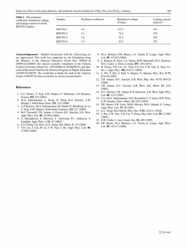
The frequency (f ) dependence of dielectric constant (ε)and the loss component (tan δ) are measured for all the sam-ples from 102 to 106 Hz at room temperature. As shown inFig. 4(a), all the BNCTO samples exhibit giant dielectric be-havior. In the whole frequency range, the dielectric constantkeeps at a giant value between ∼5 × 10³ and ∼4.5 × 10⁵.With increasing grain size, the dielectric constant increasesgradually, which is in accordance with the results of CCTOceramics [8–11, 13]. The dielectric constants for BNCTO-1, BNCTO-2, BNCTO-3, and BNCTO-4 samples at 1 kHzare 14110, 20004, 27694, and 36183, respectively. It canbe observed that the dielectric constant of all the BNCTOsamples remains almost constant in a wide frequency rangefrom 102 to 105 Hz. The dramatic decrease of dielectric con-stant is found near 106 Hz, which is related to the presenceof conductive grains [13]. Figure 4(b) shows the frequency(f ) dependence of dielectric loss (tan δ). It can be seen in
Fig. 4 Frequency (f ) dependence of dielectric constant (ε) and theloss component (tan δ) for all the BNCTO samples
382 Y. Qiu et al.
Fig. 5 Current density–electric field (J–E) characteristics for all theseBNCTO samples at room temperature. The inset plot shows the log-scale correlation of current density and electric field
this figure, the dielectric loss decreases with increasing grainsize. The minimum values of dielectric loss are 0.18, 0.13,0.11, and 0.09 at 15–20 kHz for BNCTO-1, BNCTO-2, andBNCTO-3 and BNCTO-4 samples, respectively.
The giant dielectric effect can be explained by the inter-nal barrier layer capacitors (IBLC) model [13, 14]. Accord-ing to IBLC model, the ceramic consists of n-type semi-conductive grains and insulating grain boundaries [13, 14].The dielectric constant of BNCTO ceramic specimens canbe simply expressed as the following [18]:
ε ≈ εgbd/t (1)
where εgb is the dielectric constant of the insulting grainboundary layer, d is the mean grain size, and t is the thick-ness of grain boundary-layer. It reveals that the dielectricconstant increases with decreasing boundary-layer thicknessand increasing mean grain size. According to the SEM pat-terns, with the increasing sintering durations, the growthof semiconductive grains are observed obviously, but thechanges of grain boundary regions can not be found on theouter surfaces of semiconductive grains, which contributesto the increasing of dielectric constant. The results indicatethat the dielectric constant is strongly dependent on the grainsize and well support the IBLC model.
The current density–electric field (J–E) characteristicsof all the BNCTO samples at room temperature are shown inFig. 5. It can be found that all the samples exhibit nonlinearelectrical behavior. The mathematical analysis of the currentand voltage characteristic for a varistor can be empiricallyexpressed by [19]:
I = KV α (2)
where K is a constant, and α is the nonlinear coefficient.From (2), the nonlinear coefficient α can be described by
α = (d log I )/(d logV ) (3)
Generally, α is obtained within the current density rangeof 1–10 mA/cm2. The major nonlinear electrical parame-ters are shown in Table 1. The inset plot shows the log-scale
correlation of current density and electric field. As grainsize increases, the breakdown voltage drops quickly from112.5 V/mm for BNCTO-1 to 43.2 V/mm for BNCTO-4. The nonlinear coefficients of BNCTO-1, BNCTO-2,BNCTO-3, and BNCTO-4 determined by liner fitting are4.9, 4.1, 3.8, and 3.4, respectively. And the leakage currentincreases from 455 µA/cm2 to 552 µA/cm2 when the graingrows from 1.4 µm to 4.3 µm.
The pronounced nonlinear electrical behavior for all theBNCTO samples is attributed to the Schottky-type electro-static barriers at the grain boundaries with many trap states[6, 7, 16, 20]. As for the origin of the Schottky-type elec-trostatic barriers, the model based on the role of oxygen iswidely accepted [16]. In this model, oxygen plays a key rolein forming electrically insulating phases or segregation re-gions at the grain boundary regions [16]. Such a configu-ration enables the Schottky-type electrostatic barriers to beformed at the grain boundary interfaces. Here, the grain-size-dependent breakdown voltage is similar to CCTO andother traditional varistors [7–10]. The breakdown voltagecan be expressed as the following:
E1 mA/cm2 = Ngb × Egb = (D/d) × Egb (4)
where E1 mA/cm2 is the breakdown voltage, Ngb is the num-ber of grain boundaries, Egb is the breakdown voltage ofper grain boundary, D is the thickness of sample, and d isthe mean grain size. Base on (4), the breakdown voltage de-clines when the grain size increases, which is related to thereduction of grain boundaries. Our experimental results im-ply that grain size can adjust the nonlinear electrical behav-ior of BNCTO ceramics and reveal that the grain bound-ary interfaces act as electrical potential barriers. As a result,BNCTO should be of great interest for applications involv-ing efficient varistor devices and surge protectors.
4 Conclusions
In summary, single phase BNCTO ceramics with differ-ent grain sizes have been prepared via a modified Pechinimethod. The grain size effect on the giant dielectric andnonlinear electrical behaviors are investigated in detail. Mi-crostructure analysis by SEM implies that longer sinteringduration contributes to the growth of grains. Both giant di-electric effect and nonlinear electrical behavior are stronglydependent on the grain size. The internal barrier layer ca-pacitor (IBLC) model and the IBLC model of Schottky typepotential barrier can be utilized to well interpret the grainsize effect of both the giant dielectric and nonlinear elec-trical behaviors. With grain growth, the dielectric constantincreases, in accompany with the reduction of nonlinear co-efficient and breakdown voltage. Therefore, we suggest thatthe grain size can adjust the giant dielectric and nonlinearelectrical properties of BNCTO ceramics.
Grain size effect on the giant dielectric and nonlinear electrical behaviors of Bi1/2Na1/2Cu3Ti4O12 ceramics 383
Table 1 The nonlinearcoefficient, breakdown voltage,and leakage current of all theBNCTO samples
Samples Nonlinear coefficient Breakdown voltage(V/mm)
Leakage current(µA/cm2)
BNCTO-1 4.9 112.5 455
BNCTO-2 4.1 74.2 479
BNCTO-3 3.8 54.3 529
BNCTO-4 3.4 43.2 552
Acknowledgements Helpful discussions with Dr. Chen-Liang Luare appreciated. This work was supported by the Foundation fromthe Ministry of the National Education (Grant Nos. 309020 &20090142120069), the special scientific foundation at the ChineseCentral University (Grant Nos. 20102D006 & 2010QN035), and Spe-cialized Research Fund for the Doctoral Program of Higher Education(20100142120079). We would like to thank the staff of the AnalysisCenter of HUST for their assistance in various measurements.
References
1. C.C. Homes, T. Vogt, S.M. Shapiro, S. Wakimoto, A.P. Ramirez,Science 293, 673 (2001)
2. M.A. Subramanian, L. Dong, N. Duan, B.A. Reisner, A.W.Sleight, J. Solid State Chem. 151, 323 (2000)
3. A.P. Ramirez, M.A. Subramanian, M. Gardel, G. Blumberg, D. Li,T. Vogt, S.M. Shapiro, Solid State Commun. 115, 217 (2000)
4. M.C. Ferrarelli, T.B. Adams, A. Feteira, D.C. Sinclair, A.R. West,Appl. Phys. Lett. 89, 212904 (2006)
5. C. Masingboon, S. Maensiri, T. Yamwong, P.L. Anderson, S.Seraphin, Appl. Phys. A 91, 87 (2008)
6. S.Y. Chung, I.D. Kim, S.J.L. Kang, Nat. Mater. 3, 774 (2004)7. Y.H. Lin, J. Cai, M. Li, C.W. Nan, J. He, Appl. Phys. Lett. 88,
172902 (2006)
8. M.A. Ramirez, P.R. Bueno, J.A. Varela, E. Longo, Appl. Phys.Lett. 89, 212102 (2006)
9. L. Ramajo, R. Parra, J.A. Varela, M.M. Reboredo, M.A. Ramirez,M.S. Castro, J. Alloys Compd. 497, 349 (2010)
10. B. Cheng, Y.H. Lin, J.C. Yuan, J.N. Cai, C.W. Nan, X. Xiao, J.L.He, J. Appl. Phys. 106, 034111 (2009)
11. L. Wu, Y. Zhu, S. Park, S. Shapiro, G. Shirane, Phys. Rev. B 71,014118 (2005)
12. T.B. Adams, D.C. Sinclair, A.R. West, Phys. Rev. B 73, 094124(2006)
13. T.B. Adams, D.C. Sinclair, A.R. West, Adv. Mater. 14, 1321(2002)
14. D.C. Sinclair, T.B. Adams, F.D. Morrison, A.R. West, Appl. Phys.Lett. 80, 2153 (2002)
15. J. Li, M.A. Subramanian, H.D. Rosenfeld, C.Y. Jones, B.H. Toby,A.W. Sleight, Chem. Mater. 16, 5223 (2004)
16. P.R. Bueno, E.R. Leite, M.M. Oliveira, M.O. Orlandi, E. Longo,Appl. Phys. Lett. 79, 48 (2001)
17. G.C. Deng, Paul Muralt, Phys. Rev. B 81, 224111 (2010)18. J. Wu, C.W. Nan, Y.H. Lin, Y. Deng, Phys. Rev. Lett. 89, 217601
(2002)19. D.R. Clarke, J. Am. Ceram. Soc. 82, 485 (1999)20. P.R. Bueno, M.A. Ramirez, J.A. Varela, E. Longo, Appl. Phys.
Lett. 89, 191117 (2006)