Embed Size (px)
Citation preview

Graphene and Graphene-like Molecules: Prospects in Solar CellsKian Ping Loh,* Shi Wun Tong, and Jishan Wu
Department of Chemistry and Centre for Advanced 2D Materials, National University of Singapore, 3 Science Drive 3, 117543Singapore
ABSTRACT: Graphene is constantly hyped as a game-changer for flexible transparent displays. However, to date,no solar cell fabricated on graphene electrodes has out-performed indium tin oxide in power conversion efficiency(PCE). This Perspective covers the enabling roles thatgraphene can play in solar cells because of its uniqueproperties. Compared to transparent and conducting metaloxides, graphene may not have competitive advantages interms of its electrical conductivity. The unique strength ofgraphene lies in its ability to perform various enabling rolesin solar cell architectures, leading to overall improvementin PCE. Graphene can serve as an ultrathin andtransparent diffusion barrier in solar cell contacts, as anintermediate layer in tandem solar cells, as an electronacceptor, etc. Inspired by the properties of graphene,chemists are also designing graphene-like molecules inwhich the topology of π-electron array, donor−acceptorstructures, and conformation can be tuned to offer a newclass of light-harvesting materials.
■ INTRODUCTION
Graphene, an atomic layer of carbon arranged in a honeycomblattice, has inspired a whole new generation of research on thephysics of two-dimensional materials. Right from the early days,photovoltaics had already been considered as a promising areafor the use of graphene. Could graphene be considered a next-generation electrode for organic photovoltaic devices (OPVs)?The optical transparency, high carrier mobility, flexibility, andlarge-scale processibility of graphene have frequently been citedas reasons for applying it as transparent and conductingelectrodes in solar cells.1−6 Table 1 compares the performanceof graphene to that of carbon nanotubes (CNTs) and silver-based transparent and conducting electrodes, and it can be seenthat graphene is indeed very competitive. However, no OPVcontaining a graphene electrode has out-performed indium tinoxide (ITO) to date, although recent results show that theperformance gap is closing.7 For real-world applications to cometo fruition, we have to exploit the strengths of graphene. It is ourperspective that graphene can be used not just as electrodes butas different components in the solar cell, to serve a diverse rangeof functions (Figure 1). This calls for different processingmethods for graphene. On the other hand, a new class ofgraphene-like molecules have been synthesized that offerreasonably high performance compared to traditional, full-erene-based bulk heterojunctions. There is plenty of rooms forfurther developments in terms of the synthetic versatility andstructural diversity of these graphene-like molecules.
■ GRAPHENE AS A TRANSPARENT ELECTRODECoating graphene on a glass or polymer support to fabricate atransparent conducting electrode allows conventional OPVconfigurations to be tested (Table 1).8−11 However, afundamental material limitation hinders this possibility. Thesheet resistance of graphene can be derived as Rs = (σ2dN)
−1,whereN is the number of layers and σ2d is the conductivity of the2-D sheet. It is calculated as ∼6.4 kΩ for monolayer graphene,which is far inferior to that of ITO.12 In theory, stacking graphenein a layer-by-layer manner can improve the sheet conductivity.However, multi-layer graphene is constrained by the trade-offbetween conductivity and transparency. The thickness of thegraphene used typically cannot exceed four layers, since three-layer graphene has an experimentally measured sheet resistanceof∼300Ω/sq and a transparency of∼92% at λ = 550 nm.7 Thesevalues are respectable but lag behind those of many sputteredmetal oxide films.Despite this limitation, there are attractive arguments for the
use of graphene as an electrode. Being an atomic sheet consistingof only surfaces, graphene’s Fermi level, carrier density, and workfunction can be readily tuned by surface treatment; thus, it can beused as either an anode or a cathode. The ambipolar nature ofgraphene does not allow it to show good rectificationcharacteristics unless an appropriate surface treatment is carriedout to block electron or hole injection. Doping may also benecessary, both to increase the carrier concentration and to shiftthe Fermi level of graphene for efficient carrier extraction acrossthe interface with the active layer.1
Received: October 19, 2015Published: December 10, 2015
Figure 1. Graphene that has been treated appropriately can be used asdifferent components in a solar cell, including cathode, anode, andphotoactive layers.
Perspective
pubs.acs.org/JACS
© 2015 American Chemical Society 1095 DOI: 10.1021/jacs.5b10917J. Am. Chem. Soc. 2016, 138, 1095−1102
Why not use thicker graphene sheets to achieve higherconductivity? At present, it is not easy to control the uniformityof multi-layer graphene grown by chemical vapor deposition(CVD). For layer-by-layer stacked CVD graphene, the expectedscaling behavior between thickness and conductivity is oftencompromised by the poor electronic coupling between thestacked CVD graphene sheets owing to the presence of organicresidues and trapped air pockets from the transfer process. Theseproblems are amplified in large-area electronic devices, where theseries resistance scales with the lateral dimension. Unless specialcare is taken, transferred graphene films are rarely wrinkle-free.Wrinkles are produced by capillary forces during wet transfer;they trap air pockets and prevent good electronic couplingbetween the graphene layers. There is a need to “iron out”wrinkles in graphene and “hot press” the graphene sheets toensure that the distance between the layers is within the typicalvan der Waals bonding distance. Recently, we have shown thatthe plane-to-plane tunneling conductivity of stacked CVDgraphene layers can be improved by several orders of magnitudeby inserting a self-assembledmonolayer (1-pyrenebutyric acidN-hydroxysuccinimide ester) between the graphene layers.13 Themolecular layer plays dual roles as a molecular bridge betweenthe stacked layers and a hole-dopant for the graphene. The strongbinding between the molecules and the graphene also supplantspolymeric transfer residues on the graphene surface, leading togreater planarization of the graphene.Major efforts have been directed at improving the sheet
conductivity of graphene by doping. Most of these qualify as“quick and dirty” chemical methods in which nitric acid,tetracyanoquinodimethane, and AuCl3 are commonlyused.14−16 However, exposure to air and moisture results indegradation of the doping effect with time. Clearly, a more robustway of doping is needed for realizing long-term stability.Ozyilmaz and Ahn17 achieved this by supporting an OPV onan ultrathin ferroelectric film. The non-volatile electrostaticpotential created by dipoles in the ferroelectric polymerpoly(vinylidene fluoride-co-trifluoroethylene) dopes the gra-phene (70 Ω/sq at 87% transparency). Supporting graphene on
polymer substrates offers the added advantages of flexibility,good mechanical stability, and durability.Thermal annealing in a controlled oxygen atmosphere induces
∼1013 cm−2 p-type doping of graphene. However, furtherreactivity in ambient atmosphere sometimes creates instabilitydue to permeation of adsorbates between graphene and thesubstrate. The influence of ambient adsorbates on defects ingraphene leads to an overall offset toward p-doping, maskingintrinsically n-doped samples. Owing to this, the stable n-typedoping of graphene is more challenging than p-doping, and theperformance of devices with n-doped graphene junctions istypically low.18 The photoinduced doping of graphene underlight illumination provides another strategy to achieve stable, on-demand doping. For example, the photoinduced modulation ofdoping in graphene/boron nitride heterostructures, where thedopants were separated from the conducting channel, resulted ina controllable n-type transport behavior of graphene with thepreservation of high mobility under visible light illumination.19
To date, when organic photoactive dyes have been used,graphene-on-glass electrodes have not outperformed the powerconversion efficiency (PCE) of ITO. In addition to the need forgood conductivity and transparency, the interface energy offsetbetween graphene and the photoactive material has to bematched to optimize charge transfer. Surface wettability isanother problem as the hydrophobic graphene prevents certainhole or electron transport layers from being coated well. Time-resolved surface photoresponse measurements show that p-doped graphene actually extracts electrons and competes withacceptor molecules for electron extraction; thus, it functionsbetter as a cathode.20 Recently, Gradecak et al. showed thatcoating graphene with an appropriately treated electron-blockingor transport layer is critical for its use as an anode or a cathode.7
On a conventional anode-based OPV architecture usingpoly(3,4-ethylenedioxythiophene)-poly(styrenesulfonate) (PE-DOT:PSS) as a hole injection layer and PTB7/PC71BM as thephotoactive layer, they showed that thermally annealing theelectron-blocking MoO3 layer before spin-coating the organicphotoactive layer allows a record-high PCE (6.1%) to be attainedfor a graphene anode, which is closely comparable with that of an
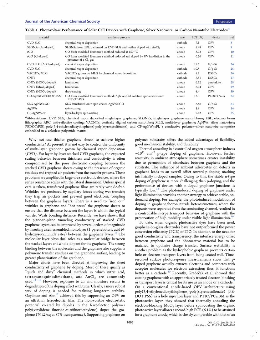
Table 1. Photovoltaic Performance of Solar Cell Devices with Graphene, Silver Nanowire, or Carbon Nanotube Electrodesa
material synthesis process role PCE (%) device ref
CVD SLG chemical vapor deposition cathode 7.1 OPV 8SLGNRs (Au-doped) SLGNRs from EBL patterned on CVD SLG and further doped with AuCl3 anode 8.48 OPV 9rGO GO from modified Hummer’s method reduced at 150 °C anode 8.02 OPV 10rGO (Cl-doped) GO from modified Hummer’s method reduced and doped by UV irradiation in the
presence of a Cl2 gasanode 6.56 OPV 11
CVD SLG (AuCl3-doped) chemical vapor deposition anode 15.6 G/n-Si 24CVD SLG chemical vapor deposition cathode 10.5 G/p-Si 25VACNTs/MLG VACNTs grown on MLG by chemical vapor deposition cathode 8.2 DSSCs 26CNTs chemical vapor deposition cathode 5.81 DSSCs 27CNTs (HNO3-doped) lamination anode 6.32 perovskite 28CNTs (MoOx-doped) lamination anode 6.04 OPV 29CNTs (HNO3-doped) drop-casting anode 4.4 OPV 30GO:AgNWs/PEDOT:PSS GO from modified Hummer’s method; AgNWs:GO solution spin-coated onto
PEDOT:PSSanode 13.3 PEDOT/n-Si 32
SLG-AgNWs:GO SLG transferred onto spin-coated AgNWs:GO anode 8.68 G/n-Si 33AgNWs spin-coating anode 5.8 OPV 34CP-AgNW/cPI layer-by-layer spin-coating anode 7.42 OPV 35
aAbbreviations: CVD SLG, chemical vapor deposited single-layer graphene; SLGNRs, single-layer graphene nanoribbons; EBL, electron beamlithography; ARC, anti-reflective coating; VACNTs, vertically aligned carbon nanotubes; MLG, multi-layer graphene; AgNWs, silver nanowires;PEDOT:PSS, poly(3,4-ethylenedioxythiophene)-poly(styrenesulfonate); and CP-AgNW/cPI, a conductive polymer−silver nanowire compositeembedded in a colorless polyimide matrix.
Journal of the American Chemical Society Perspective
DOI: 10.1021/jacs.5b10917J. Am. Chem. Soc. 2016, 138, 1095−1102
1096

ITO reference electrode (PCE = 6.7%). They also demonstratedthe use of graphene in an inverted cathode-based solar cell usingn-type ZnO as the electron transport layer, where the deviceperformance also approached that of ITO.
■ GRAPHENE SCHOTTKY BARRIER CELLSMoving beyond the use of graphene-on-glass or graphene-on-polymer, the innovative use of graphene in other types of solarcell architectures has begun to emerge. Such efforts takeadvantage of graphene’s tunable work function and itsdiffusion-barrier properties. Several niche applications havebeen demonstrated for graphene in various solar cellarchitectures, ranging from silicon p-n solar cells to theirSchottky barrier counterparts.In a conventional silicon p-n junction solar cell, the diffusion of
metals from the metal contacts into Si can cause unwanteddoping and lead to the formation of deep trap levels. Cu and Au,which are among the most widely used interconnects, diffusesignificantly into Si. The use of a dielectric barrier such as TaN orTiN is undesirable, as it can change the junction properties.Commercial Si-based solar cells avoid this problem bysubstituting Cu with expensive Ag, as the latter diffuses moreslowly. Graphene is found to be an excellent protective barrieragainst Cu and Al diffusion, and it does not modify the Schottkybarrier of copper on silicon.21 In addition, graphene is atomicallythin and allows electrons to tunnel through it easily. Thus,graphene can be employed as a diffusion barrier for copperelectrodes and as interconnects in solar cells.Extending beyond this, graphene can also be used effectively as
a top electrode in Schottky barrier solar cells. In a traditionalSchottky barrier cell, a thin transparent metal layer is depositedon an n-type silicon interface, leading to a positively chargeddepletion region as donor electrons are transferred across theinterface. In a graphene Schottky barrier solar cell, graphenereplaces the metal, and the barrier height is given essentially bythe difference in work function between graphene and the n-doped semiconductor.22,23 One advantage is that graphene’sFermi level and work function can be readily tuned by doping.Song et al. reported a new record efficiency of 15.6% in CVDgraphene anode/n-silicon devices with an anti-reflective coatingand suitably doped graphene.24 By doping the graphene withAuCl3 and carefully optimizing the silicon oxide thickness at thegraphene/Si interface to minimize carrier recombination, ahigher fill factor can be attained. To achieve stable doping, theconcept of sunlight-activated, tunable n-doping of graphene wasdemonstrated by Chen et al., who developed a graphene/TiOxcathode to be used in a graphene/Si Schottky junction solarcell.25 With its intrinsic n-type doping, the TiOx thin layer acts asan electron-donating agent, increasing the electron concen-tration and the Fermi level of graphene. Upon illumination,photoexcited electrons from TiOx are transferred to graphene,further increasing the n-doping and Schottky barrier heights atthe graphene/p-Si junction. A good PCE (>10%) can beobtained. It can be appreciated that such photoinduced doping ofgraphene under light illumination provides a more stable form ofdoping than chemical doping.25
Another emerging area is the use of graphene as a cathode indye-sensitized solar cells (DSSCs). Dong et al. reported a novelcathode made from 150-μm-long CNTs grown on catalyst-covered graphene, which has the potential to replace theexpensive and brittle platinum-based materials used in conven-tional DSSC photovolatics.26 Numerous reports have shown thatstand-alone CNTs can act as good electrodes in solar cells, with
efficiency ranging from 4.4% to 6.32% (Table 1).27−30 A hybridgraphene/CNT electrode has lower charge-transfer resistancewith the electrolyte (20 times smaller than for platinum-basedcathodes) owing to its large surface area. DSSCs utilizing thisflexible, vertically aligned CNT/graphene hybrid cathodeoutperformed Pt-based cells in both rigid (8.2% vs 6.4%) andflexible (3.9% vs 3.4%) assemblies.The above discussion is based on graphene grown by CVD
with the hope that roll-to-roll growth-and-transfer technologywill address the scaling issues faced in the implementation oflarge-area devices. Parallel to CVD graphene, numerous researchefforts have focused on liquid-phase exfoliated graphene orgraphene oxide (GO). Owing to its defective and insulatingnature, the sheet resistance of GO or reduced graphene oxide(rGO) is too high to compete against ITO; however, its solution-processibility opens up many alternative functions, such as holetransport and charge relay. GO is particularly well suited as amatrix for supporting conducting silver nanowires (AgNWs).For example, insulating GO flakes have been used as anovercoating layer and protecting layer for a conductive-nanowire-based indium-free transparent conductive film, inwhich large-area scalability has been demonstrated.31 Thesandwich structure formed by a AgNWs network betweenPEDOT:PSS and GO was reported to have lower resistivity thanITO,32 and a high PCE = 13.3% could be obtained, which isbetter than that of electrodes fabricated entirely from AgNWcomposites (Table 1).33−35 Chhowalla et al. also demonstratedthat GO, which can be deposited from a neutral solution and isnon-damaging to ITO, is as efficient as PEDOT:PSS in terms offunctioning as a hole transport and electron blocking layer in anOPV device.36
■ GRAPHENE IN PEROVSKITES-BASED SOLAR CELL
Recently, a new type of solar cell based on organic−inorganichalide perovskites has witnessed rapid development. Althoughfurther optimization seems possible, its PCE has alreadysurpassed 20% since its first development in 2009. Graphenecan be utilized to improve the device performance and yieldduring the fabrication of perovskite-based solar cells.37−40 Forexample, the use of high-temperature sintered TiO2 as theelectron transport layer in perovskite-based solar cells isdisadvantageous, owing to its high cost and slow production.To address this, Wang et al. employed low-temperatureprocessed nanocomposites of pristine graphene nanoflakes andanatase-TiO2 nanoparticles in the electron transport layer inperovskite-based solar cells.37 Remarkable photovoltaic perform-ance with efficiency up to 15.6% is achievable with thisnanocomposite, owing to the good energy level alignmentbetween graphene and its adjacent layers (fluorine tin oxide andTiO2) as well as the good carrier mobility of graphene. Graphenecan also be used to extract electrons efficiently from TiO2, thusleaving fewer electrons in TiO2 to undergo recombination withthe holes in perovskites. Printable inks made from conductinggraphene and TiO2 nanoparticles should be highly useful inprintable solar cell technology. The integration of metal trihalideperovskites37 and graphene may lead to the development of aprintable, roll-to-roll process for the large-scale manufacturing ofa new type of solar cell, where graphene plays the dual roles ofpassivating layer and electrode to the perovskite.
Journal of the American Chemical Society Perspective
DOI: 10.1021/jacs.5b10917J. Am. Chem. Soc. 2016, 138, 1095−1102
1097
■ GRAPHENE AS INTERMEDIATE LAYERS IN TANDEMCELLS
The tandem solar cell concept boosts device efficiency bystacking two or more single-junction cells with different bandgaps, such that the effective absorption window is thecombination of them all. An intermediate layer (IML) is neededto join the stacked cells so that they can harvest complementaryabsorption spectra without significant optical and electroniclosses. Generally, an efficient IML must fulfill three require-ments: (i) act as a good recombination layer for electron andholes, (ii) have minimal light absorption, and (iii) act as aprotective layer to prevent intermixing of two subcells. Toprevent intermixing problems, the IML has to be a continuous,compact layer. Hadipour et al. reported that the thinnestcontinuous metal layer required to protect the bottom devicefrom being destroyed during the fabrication of the top device is10−15 nm.41 Although such thick metal layers can act as aprotective and conductive IML in the parallel tandem cells, the40−60% loss in light transmission due to the poor transparencyof Au,42 Al/Ag,43 and Al/Au44 becomes a disadvantage.Transparent IMLs consisting of AgNW films45 or CNTs
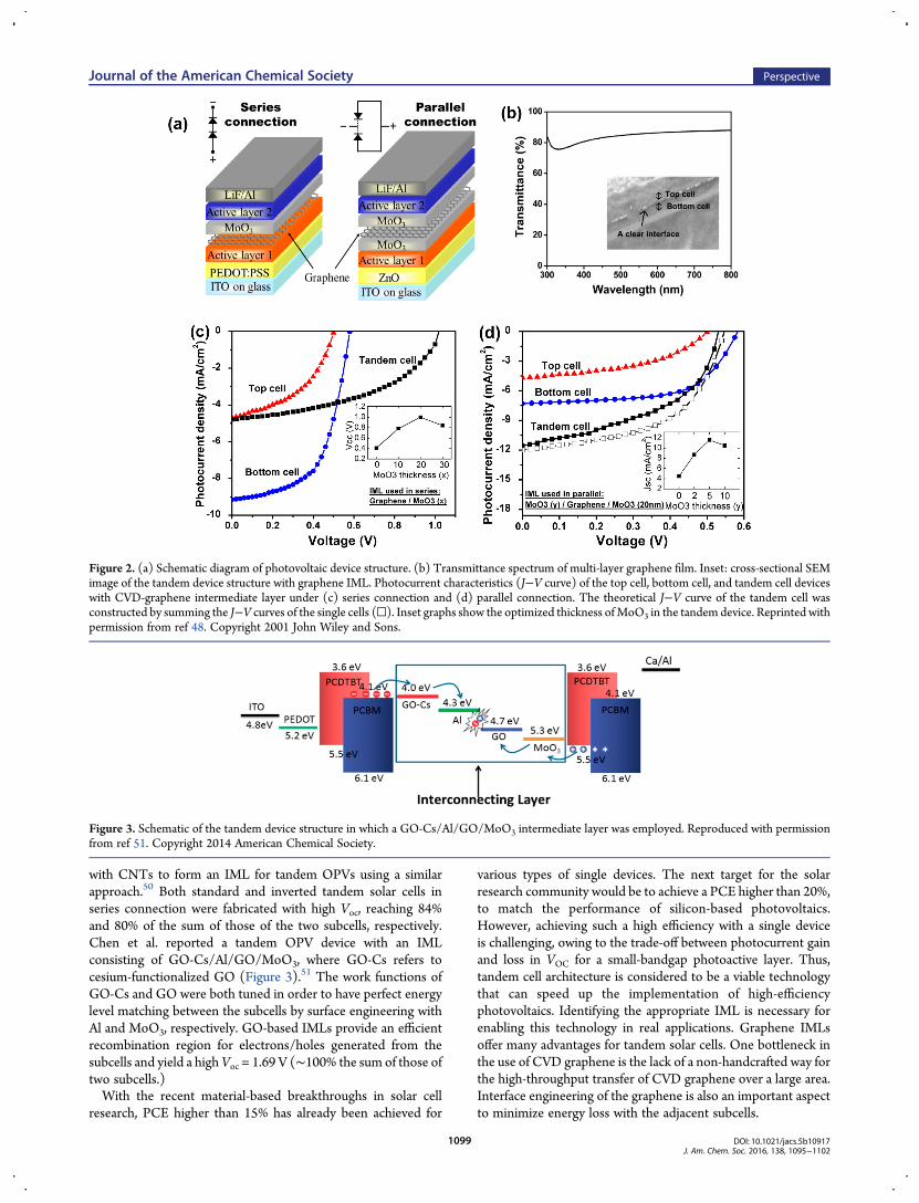
films46,47 have been developed to replace the conventional metalIML (Table 2). They can be solution-processed and afford a lighttransmission of >80%, which is better than that possible withmetal contacts. However, the high surface roughness of AgNWsand the large contact resistance between CNTs/organicmaterials pose problems for their use as IMLs. Due to itstransparency, high conductivity, multi-layer CVD graphene hasbeen utilized as IML in both series-connected and parallel-connected tandem OPV devices (Figure 2a).48 Thus far, mostIMLs employ a series connection rather than a parallelconnection, owing to the limited availability of IMLs with highin-plane conductivity. In a series-connected tandem cell, adiscontinuous metallic IML is sufficient to ensure efficientrecombination between two subcells. In contrast, the IML isrequired to act as a highly conductive, transparent, andcontinuous electrical contact in parallel connection because ofthe lateral flow of current. Indeed, there is a strong demand todevelop parallel-connected tandem cells in which two subcellscan operate individually. Compared with series-connected
tandem cells, high efficiency can be more readily achieved inparallel tandem cells without the strict criterion for photocurrentmatching. CVD graphene satisfies most of the criteria for use asan IML for both parallel and series connections. CVD-growngraphene film (<1 kΩ/sq) with high transparency (>80% at 550nm) has been demonstrated to be a good IML between twosubcells, as shown in Figure 2b. The high in-plane conductivity ofgraphene prevents charge buildup between subcells. The workfunction of graphene is in the range between 4.2 and 4.6 eV,which is too low for efficient hole extraction. Efficient holeextraction can be achieved after coating graphene with MoO3 toincrease the work function to 5.5 eV.48 By using graphene/MoO3IML in series-connected tandem cells, a favorable energy leveloffset was induced at the IML/subcells interfaces, leading toefficient recombination of electrons from the bottom cell andholes from the top cell. In parallel-connected tandem cells, thehigh work function of a sandwiched MoO3/graphene/MoO3IML could extract the holes from ITO and LiF/Al cathodeseffectively. As shown in Figure 2c,d, the values of open-circuitvoltage (Voc) and short-circuit current density (Jsc) in the tandemcell are very close to the sum values of Voc and Jsc from the twosingle subcells in series and parallel connections, respectively,further confirming the good ohmic contact at the active layer/MoO3-modified graphene interface. The nearly identicaltheoretical curve and experimental result obtained with thetandem cell (Figure 2d) suggests that a MoO3/graphene/MoO3layer serves as an effective IML in parallel-connected tandemcells. Even without perfect current matching between twosubcells, the efficiency of the parallel tandem cell can reach 88%of the sum of those of the two subcells.48
Solution-processed GO has also been applied as IML in series-connected tandem devices, as shown in Table 2.49−51 Advantagesinclude the ease of spin-coating GO, as well as its ability to formcomposites with polymer. Tung et al. mixed GOwith conductingpolymer PEDOT:PSS to make a sticky gel with higher electricalconductivity.49 Using GO/PEDOT:PSS as an adhesive IML, twoP3HT:PCBM bulk heterojunctions were stacked together by adirect adhesive lamination process without significant ohmic loss.The high Voc of the tandem device was 0.94 V, reaching 84% ofthe sum of those of the two subcells. GO has also been mixed
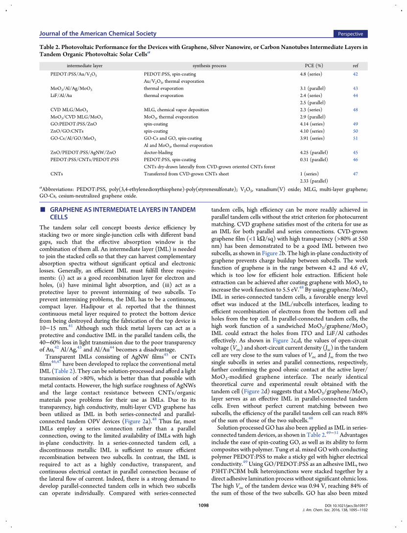
Table 2. Photovoltaic Performance for the Devices with Graphene, Silver Nanowire, or Carbon Nanotubes Intermediate Layers inTandem Organic Photovoltaic Solar Cellsa
intermediate layer synthesis process PCE (%) ref
PEDOT:PSS/Au/V2O5 PEDOT:PSS, spin-coating 4.8 (series) 42Au/V2O5, thermal evaporation
MoO3/Al/Ag/MoO3 thermal evaporation 3.1 (parallel) 43LiF/Al/Au thermal evaporation 2.4 (series) 44
2.5 (parallel)CVD MLG/MoO3 MLG, chemical vapor deposition 2.3 (series) 48MoO3/CVD MLG/MoO3 MoO3, thermal evaporation 2.9 (parallel)GO:PEDOT:PSS/ZnO spin-coating 4.14 (series) 49ZnO/GO:CNTs spin-coating 4.10 (series) 50GO-Cs/Al/GO/MoO3 GO-Cs and GO, spin-coating 3.91 (series) 51
Al and MoO3, thermal evaporationZnO/PEDOT:PSS/AgNW/ZnO doctor-blading 4.25 (parallel) 45PEDOT:PSS/CNTs/PEDOT:PSS PEDOT:PSS, spin-coating 0.31 (parallel) 46
CNTs dry-drawn laterally from CVD-grown oriented CNTs forestCNTs Transferred from CVD-grown CNTs sheet 1 (series) 47
2.33 (parallel)aAbbreviations: PEDOT:PSS, poly(3,4-ethylenedioxythiophene)-poly(styrenesulfonate); V2O5, vanadium(V) oxide; MLG, multi-layer graphene;GO-Cs, cesium-neutralized graphene oxide.
Journal of the American Chemical Society Perspective
DOI: 10.1021/jacs.5b10917J. Am. Chem. Soc. 2016, 138, 1095−1102
1098
with CNTs to form an IML for tandem OPVs using a similarapproach.50 Both standard and inverted tandem solar cells inseries connection were fabricated with high Voc, reaching 84%and 80% of the sum of those of the two subcells, respectively.Chen et al. reported a tandem OPV device with an IMLconsisting of GO-Cs/Al/GO/MoO3, where GO-Cs refers tocesium-functionalized GO (Figure 3).51 The work functions ofGO-Cs and GO were both tuned in order to have perfect energylevel matching between the subcells by surface engineering withAl and MoO3, respectively. GO-based IMLs provide an efficientrecombination region for electrons/holes generated from thesubcells and yield a highVoc = 1.69 V (∼100% the sum of those oftwo subcells.)With the recent material-based breakthroughs in solar cell
research, PCE higher than 15% has already been achieved for
various types of single devices. The next target for the solarresearch community would be to achieve a PCE higher than 20%,to match the performance of silicon-based photovoltaics.However, achieving such a high efficiency with a single deviceis challenging, owing to the trade-off between photocurrent gainand loss in VOC for a small-bandgap photoactive layer. Thus,tandem cell architecture is considered to be a viable technologythat can speed up the implementation of high-efficiencyphotovoltaics. Identifying the appropriate IML is necessary forenabling this technology in real applications. Graphene IMLsoffer many advantages for tandem solar cells. One bottleneck inthe use of CVD graphene is the lack of a non-handcrafted way forthe high-throughput transfer of CVD graphene over a large area.Interface engineering of the graphene is also an important aspectto minimize energy loss with the adjacent subcells.
Figure 2. (a) Schematic diagram of photovoltaic device structure. (b) Transmittance spectrum of multi-layer graphene film. Inset: cross-sectional SEMimage of the tandem device structure with graphene IML. Photocurrent characteristics (J−V curve) of the top cell, bottom cell, and tandem cell deviceswith CVD-graphene intermediate layer under (c) series connection and (d) parallel connection. The theoretical J−V curve of the tandem cell wasconstructed by summing the J−V curves of the single cells (□). Inset graphs show the optimized thickness ofMoO3 in the tandem device. Reprinted withpermission from ref 48. Copyright 2001 John Wiley and Sons.
Figure 3. Schematic of the tandem device structure in which a GO-Cs/Al/GO/MoO3 intermediate layer was employed. Reproduced with permissionfrom ref 51. Copyright 2014 American Chemical Society.
Journal of the American Chemical Society Perspective
DOI: 10.1021/jacs.5b10917J. Am. Chem. Soc. 2016, 138, 1095−1102
1099

■ GRAPHENE-LIKE MOLECULES FOR SOLAR CELLS
Benzenoid polycyclic aromatic hydrocarbons can be regarded asgraphene-like molecules, and strong intermolecular π−πinteractions usually drive them into one-dimensional self-assembled columnar structures with high charge carriermobility.52 Depending on the electron-rich or electron-deficientnature, various graphene-like molecules have been used as eitherelectron donors or electron acceptors in organic solar cells(Figure 4). Friend and Mullen first applied the disc-like liquidcrystalline hexa-peri-hexabenzocoronene (HBC) together with acrystalline perylene diimide (PDI) in photodiodes anddemonstrated efficient charge transfer between these twocomponents.53 This initialized the research into using solution-processible, small-molecule-based semiconductors for OPVs.However, the poor light-harvesting property of HBC, arisingfrom its large number of aromatic sextet rings (the hexagonshighlighted in blue in Figure 4), led to low PCEs. Later,Nuckolls’s group synthesized a series of hexa-cata-hexabenzo-coronenes (c-HBC), which turned out to have a contorted,double-concave geometry.54 c-HBC shows a radialene characterfor the central benzene ring and displays improved light-harvesting properties compared to its planar HBC counterparts.Interestingly, these non-planar molecules still can form long-range ordered columnar packing, with field-effect hole mobilityup to 0.02 cm2/(V·s) in the solution-processed thin films. Inaddition, the double-concave structure allows them to nest ball-shaped electron acceptors such as fullerene (C60). In fact, bilayerheterojunction devices using parent c-HBC and C60 exhibitedvery efficient charge transfer at this optimal ball-and-socketinterface, and high Voc up to 0.95 V was achieved. However, theoverall PCE was still low (1.04%) due to the still poor light-harvesting capability of the c-HBC.55 This was further improvedby using the thiophene analogues, the alkylated dibenzo-tetrathienocoronenes (c-DBTTC), which show very intense
absorption in the UV region and can form a self-assembled,three-dimensional network of cables.56 This scaffold provided atemplate for a reticulated heterojunction with C60 and resulted inan improved PCE of ∼2%. Ball-and-socket complexation wasalso found in the solution-processed thin films of c-HBC:PC70BM
57 and c-DBTTC:PC70BM,58 leading to amaximum PCE of 2.41% for the latter. Bathochromic absorptionwas observed for the larger-sized contorted octabenzocircum-biphenyl (c-OBCB); consequently, solar cells based on c-OBCB:PC70BM complexes gave PCEs up to 2.9%.59 Thesestudies showed that both light harvesting and molecular-scaledonor−acceptor complexation play important roles in determin-ing the solar cell’s performance. Development should focus onhow to improve light absorption in the visible and even the near-infrared regions, where absorption is weak.Graphene-like molecules, when substituted by strong electron-
withdrawing groups, can be converted into n-type semi-conductors. One good example is PDI, which shows strongabsorption in the visible region, high electron mobility, and aLUMO energy level comparable to that of typical fullerenes.Therefore, it was considered for use as a new non-fullereneacceptor in OPVs. Early tests using PDI as an electron acceptorin OPVs were not so successful, with a maximum PCE of ∼4%,mainly due to the formation of too-large crystalline PDIdomains. This situation was improved by using a twisted, bay-linked PDI dimer (di-PDI), which can form a homogeneousblend with a suitable donor polymer, giving a PCE of up to 6%.60
Very recently, a PCE as high as 7.16% was achieved when a S-annulated PDI dimer (di-PDI-S) was used as acceptor.61 On theother hand, Nuckolls et al. developed a series of vinyl-bridgedPDI oligomers (v-PDI-n, n = 1−4) with a helical, ribbon-likestructure.62 These oligomers showed good solubility in normalorganic solvents, intense absorption in the visible region, highelectron mobility, and a low-lying LUMO energy level similar to
Figure 4. Structures of various graphene-like molecules used for organic solar cells.
Journal of the American Chemical Society Perspective
DOI: 10.1021/jacs.5b10917J. Am. Chem. Soc. 2016, 138, 1095−1102
1100

those of PCBMs. OPVs from the blend of these oligomers andappropriate donor polymers give a PCE as high as 8.3%, setting arecord high for non-fullerene bulk heterojunctions. The goodperformance can be ascribed to the mesh-like network ofacceptors with pores that are tens of nanometers in diameter forefficient exciton separation and charge transport. These researchworks demonstrate that electron-accepting graphene-like mole-cules with a twisted structure could be good replacements forexpensive fullerene acceptors in OPVs. The key for furtherimprovements relies on whether we can further enhance thelight-harvesting capability, maintain high electron mobility, andfind the right donor polymer to form an optimal morphology.
■ CONCLUSIONIn summary, collective evidence from research over the years hasshown that graphene, whether grown by CVD or solution-synthesized, has found niche roles in various components of solarcells, giving rise to performance enhancement. Instead ofreplacing silicon-based photovoltaics, it is more realistic toconsider graphene as a performance enhancer in these devices.Bottom-up-synthesized graphene-like molecules have diversestructural motifs which can be tailor-made for various functions.Chemists are learning about the design principles in thesemolecules that can afford strong light harvesting and efficientexciton separation. In the future, it should be possible to realize aflexible solar cell consisting of a photoactive layer made fromgraphene-like molecules for absorption and exciton generation,and hole or electron transport layers made from solution-processed graphene, with all these components integrated on aflexible, large-area graphene electrode.
■ AUTHOR INFORMATION
Corresponding Author*[email protected]
NotesThe authors declare no competing financial interest.
■ ACKNOWLEDGMENTSThe authors like to acknowledge funding support fromMOE2014-T3-1-004.
■ REFERENCES(1) Wang, Y.; Tong, S. W.; Xu, X. F.; Ozyilmaz, B.; Loh, K. P. Adv.Mater. 2011, 23, 1514−1518.(2) Wang, Y.; Chen, X. H.; Zhong, Y. L.; Zhu, F. R.; Loh, K. P. Appl.Phys. Lett. 2009, 95, 063302.(3) He, Z. C.; Zhong, C. M.; Su, S. J.; Xu, M.; Wu, H. B.; Cao, Y. Nat.Photonics 2012, 6, 591−595.(4) Park, H.; Brown, P. R.; Bulovic, V.; Kong, J. Nano Lett. 2012, 12,133−140.(5) Wang, X.; Zhi, L.; Mullen, K. Nano Lett. 2008, 8, 323−327.(6) Wang, X.; Zhi, L.; Tsao, N.; Tomovic, Z.; Li, J.; Mullen, K. Angew.Chem., Int. Ed. 2008, 47, 2990−2992.(7) Park, H.; Chang, S.; Zhou, X.; Kong, J.; Palacios, T.; Gradecak, S.Nano Lett. 2014, 14, 5148−5154.(8) Park, H.; Chang, S.; Zhou, X.; Kong, J.; Palacios, T.; Gradecak, S.Nano Lett. 2014, 14, 5148−5154.(9) Yusoff, A. R. b. M.; Kim, D.; Schneider, F. K.; da Silva, W. J.; Jang, J.Energy Environ. Sci. 2015, 8, 1523−1537.(10) Yusoff, A. R. b. M.; Lee, S. J.; Shneider, F. K.; da Silva,W. J.; Jang, J.Adv. Energy Mater. 2014, 4, 1301989.(11) Stratakis, E.; Savva, K.; Konios, D.; Petridis, C.; Kymakis, E.Nanoscale 2014, 6, 6925−6931.
(12) Bonaccorso, F.; Sun, Z.; Hasan, T.; Ferrari, A. C. Nat. Photonics2010, 4, 611−622.(13) Liu, Y.; Yuan, L.; Yang, M.; Zheng, Y.; Li, L.; Gao, L.;Nerngchamnong, N.; Nai, C. T.; Sangeeth, C. S. S.; Feng, Y. P.; Nijhuis,C. A.; Loh, K. P. Nat. Commun. 2014, 5, 5461.(14) Lee, S.; Yeo, J.-S.; Ji, Y.; Cho, C.; Kim, D.-Y.; Na, S.-I.; Lee, B. H.;Lee, T. Nanotechnology 2012, 23, 344013.(15) Hsu, C.-L.; Lin, C.-T.; Huang, J.-H.; Chu, C.-W.; Wei, K.-H.; Li,L.-J. ACS Nano 2012, 6, 5031−5039.(16) Park, H.; Rowehl, J. A.; Kim, K. K.; Bulovic, V.; Kong, J.Nanotechnology 2010, 21, 505204.(17) Kim, K.; Bae, S.-H.; Toh, C. T.; Kim, H.; Cho, J. H.; Whang, D.;Lee, T.-W.; Ozyilmaz, B.; Ahn, J.-H. ACS Appl. Mater. Interfaces 2014, 6,3299−3304.(18) Schedin, F.; Geim, A. K.; Morozov, S. V.; Hill, E. W.; Blake, P.;Katsnelson, M. I.; Novoselov, K. S. Nat. Mater. 2007, 6, 652−655.(19) Ju, L.; Velasco, J., Jr.; Huang, E.; Kahn, S.; Nosiglia, C.; Tsai, H.-Z.;Yang, W.; Taniguchi, T.; Watanabe, K.; Zhang, Y.; Zhang, G.; Crommie,M.; Zettl, A.; Wang, F. Nat. Nanotechnol. 2014, 9, 348−352.(20) Zhang, L.; Roy, S. S.; English, C. R.; Hamers, R. J.; Arnold, M. S.;Andrew, T. L. ACS Nano 2015, 9, 2510−2517.(21) Wong, C. P. Y.; Koek, T. J. H.; Liu, Y. P.; Loh, K. P.; Goh, K. E. J.;Troadec, C.; Nijhuis, C. A. ACS Appl. Mater. Interfaces 2014, 6, 20464−20472.(22) Chen, C. C.; Aykol, M.; Chang, C. C.; Levi, A. F. J.; Cronin, S. B.Nano Lett. 2011, 11, 1863−1867.(23) Li, X. M.; Zhu, H.W.; Wang, K. L.; Cao, A. Y.; Wei, J. Q.; Li, C. Y.;Jia, Y.; Li, Z.; Li, X.; Wu, D. H. Adv. Mater. 2010, 22, 2743−2748.(24) Song, Y.; Li, X.; Mackin, C.; Zhang, X.; Fang, W.; Palacios, T.;Zhu, H.; Kong, J. Nano Lett. 2015, 15, 2104−2110.(25) Ho, P.-H.; Lee, W.-C.; Liou, Y.-T.; Chiu, Y.-P.; Shih, Y.-S.; Chen,C.-C.; Su, P.-Y.; Li, M.-K.; Chen, H.-L.; Liang, C.-T.; Chen, C.-W. EnergyEnviron. Sci. 2015, 8, 2085−2092.(26) Dong, P.; Zhu, Y.; Zhang, J.; Hao, F.; Wu, J.; Lei, S.; Lin, H.;Hauge, R. H.; Tour, J. M.; Lou, J. J. Mater. Chem. A 2014, 2, 20902−20907.(27) Hao, F.; Wang, Z.; Luo, Q.; Lou, J.; Li, J.; Wang, J.; Fan, S.; Jiang,K.; Lin, H. J. J. Mater. Chem. 2012, 22, 22756−22762.(28) Jeon, I.; Chiba, T.; Delacou, C.; Guo, Y.; Kaskela, A.; Reynaud, O.;Kauppinen, E. I.; Maruyama, S.; Matsuo, Y. Nano Lett. 2015, 15, 6665−6671.(29) Jeon, I.; Cui, K.; Chiba, T.; Anisimov, A.; Nasibulin, A. G.;Kauppinen, E. I.; Maruyama, S.; Matsuo, Y. J. Am. Chem. Soc. 2015, 137,7982−7985.(30) Dabera, G. D. M. R.; Prabhath, M. R. R.; Lai, K. T.; Jayawardena,K. D. G. I.; Sam, F. L. M.; Rozanski, L. J.; Adikaari, A. A. D. T.; Silva, S. R.P. Adv. Funct. Mater. 2015, 25, 4520−4530.(31) Moon, I. K.; Kim, J. I.; Lee, H.; Hur, K.; Kim, W. C.; Lee, H. Sci.Rep. 2013, 3, 1112.(32) Xu, Q.; Song, T.; Cui, W.; Liu, Y.; Xu, W.; Lee, S. T.; Sun, B. ACSAppl. Mater. Interfaces 2015, 7, 3272−3279.(33) Yang, L.; Yu, X.; Hu, W.; Wu, X.; Zhao, Y.; Yang, D. ACS Appl.Mater. Interfaces 2015, 7, 4135−4141.(34) Song, M.; You, D. S.; Lim, K.; Park, S.; Jung, S.; Kim, C. S.; Kim,D.-H.; Kim, D.-G.; Kim, J.-K.; Park, J.; Kang, Y.-C.; Heo, J.; Jin, S.-H.;Park, J. H.; Kang, J.-W. Adv. Funct. Mater. 2013, 23, 4177−4184.(35) Kim, Y.; Ryu, T. I.; Ok, K.-H.; Kwak, M.-G.; Park, S.; Park, N.-G.;Han, C. J.; Kim, B. S.; Ko, M. J.; Son, H. J.; Kim, J.-W. Adv. Funct. Mater.2015, 25, 4580−4589.(36) Li, S.-S.; Tu, K.-H.; Lin, C.-C.; Chen, C.-W.; Chhowalla, M. ACSNano 2010, 4, 3169.(37) Wang, J. T.-W.; Ball, J. M.; Barea, E. M.; Abate, A.; Alexander-Webber, J. A.; Huang, J.; Saliba, M.;Mora-Sero, I.; Bisquert, J.; Snaith, H.J.; Nicholas, R. J. Nano Lett. 2014, 14, 724−730.(38) Liu, T.; Kim, D.; Han, H.; Yusoff, A. R. M.; Jang, J. Nanoscale2015, 7, 10708−10718.(39) Yan, K.; Wei, Z.; Li, J.; Chen, H.; Yi, Y.; Zheng, X.; Long, X.;Wang, Z.; Wang, J.; Xu, J.; Yang, S. Small 2015, 11, 2269−2274.
Journal of the American Chemical Society Perspective
DOI: 10.1021/jacs.5b10917J. Am. Chem. Soc. 2016, 138, 1095−1102
1101
(40) Yeo, J.-S.; Kang, R.; Lee, S.; Jeon, Y.-J.; Myoung, N.; Lee, C.-L.;Kim, D.-Y.; Yun, J.-M.; Seo, Y.-H.; Kim, S.-S.; Na, S.-I. Nano Energy2015, 12, 96−104.(41) Hadipour, A.; de Boer, B.; Wildeman, J.; Kooistra, F. B.;Hummelen, J. C.; Turbiez, M. G. R.; Wienk, M. M.; Janssen, R. A. J.;Blom, P. W. M. Adv. Funct. Mater. 2006, 16, 1897−1903.(42) Sista, S.; Hong, Z.; Park, M.-H.; Xu, Z.; Yang, Y. Adv. Mater. 2010,22, E77−E80.(43) Guo, X. Y.; Liu, F. M.; Yue,W.; Xie, Z. Y.; Geng, Y. H.;Wang, L. X.Org. Electron. 2009, 10, 1174−1177.(44) Shrotriya, V.; Wu, E. H.-E.; Li, G.; Yao, Y.; Yang, Y. Appl. Phys.Lett. 2006, 88, 064104.(45) Guo, F.; Kubis, P.; Li, N.; Przybilla, T.; Matt, G.; Stubhan, T.;Ameri, T.; Butz, B.; Spiecker, E.; Forberich, K.; Brabec, C. J. ACS Nano2014, 8, 12632−12640.(46) Tanaka, S.; Mielczarek, K.; Ovalle-Robles, R.; Wang, B.; Hsu, D.;Zakhidov, A. A. Appl. Phys. Lett. 2009, 94, 113506.(47) Xia, X.; Wang, S.; Jia, Y.; Bian, Z.; Wu, D.; Zhang, L.; Cao, A.;Huang, C. J. Mater. Chem. 2010, 20, 8478−8482.(48) Tong, S.W.;Wang, Y.; Zheng, Y.; Ng,M.-F.; Loh, K. P.Adv. Funct.Mater. 2011, 21, 4430−4435.(49) Tung, V. C.; Kim, J.; Cote, L. J.; Huang, J. J. Am. Chem. Soc. 2011,133, 9262−9265.(50) Tung, V. C.; Kim, J.; Huang, J. Adv. Energy Mater. 2012, 2, 299−303.(51) Chen, Y.; Lin, W.-C.; Liu, J.; Dai, L. Nano Lett. 2014, 14, 1467−1471.(52) Wu, J.; Pisula, W.; Mullen, K. Chem. Rev. 2007, 107, 718−747.(53) Schmidt-Mende, L.; Fechtenkotter, A.; Mullen, K.; Moons, E.;Friend, R. H.; MacKenzie, J. D. Science 2001, 293, 1119−1122.(54) Xiao, S.; Myers, M.; Miao, Q.; Sanaur, S.; Pang, K.; Steigerwald,M. L.; Nuckolls, C. Angew. Chem., Int. Ed. 2005, 44, 7390−7394.(55) Tremblay, N. J.; Gorodetsky, A. A.; Cox, M. P.; Schiros, T.; Kim,B.; Steiner, R.; Bullard, Z.; Sattler, A.; So, W.-Y.; Itoh, Y.; Toney, M. F.;Ogasawara, H.; Ramirez, A. P.; Kymissis, I.; Steigerwald, M. L.; Nuckolls,C. ChemPhysChem 2010, 11, 799−803.(56) Gorodetsky, A. A.; Chiu, C. Y.; Schiros, T.; Palma, M.; Cox, M.;Jia, Z.; Sattler, W.; Kymissis, I.; Steigerwald, M.; Nuckolls, C. Angew.Chem., Int. Ed. 2010, 49, 7909−7912.(57) Kang, S. J.; Ahn, S.; Kim, J. B.; Schenck, C.; Hiszpanski, A. M.; Oh,S.; Schiros, T.; Loo, Y. L.; Nuckolls, C. J. Am. Chem. Soc. 2013, 135,2207−2212.(58) Kang, S. J.; Kim, J. B.; Chiu, C. Y.; Ahn, S.; Schiros, T.; Lee, S. S.;Yager, K. G.; Toney,M. F.; Loo, Y. L.; Nuckolls, C.Angew. Chem., Int. Ed.2012, 51, 8594−8597.(59) Xiao, S.; Kang, S. J.; Wu, Y.; Ahn, S.; Kim, J. B.; Loo, Y. L.; Siegrist,T.; Steigerwald, M. L.; Li, H. X.; Nuckolls, C. Chem. Sci. 2013, 4, 2018−2023.(60) Zang, Y.; Li, C. Z.; Chueh, C. C.; Williams, S. T.; Jiang, W.; Wang,Z. H.; Yu, J. S.; Jen, A. K. Y. Adv. Mater. 2014, 26, 5708−5714.(61) Sun, D.; Meng, D.; Cai, Y.; Fan, B.; Li, Y.; Jiang, W.; Huo, L.; Sun,Y.; Wang, Z. J. Am. Chem. Soc. 2015, 137, 11156−11162.(62) Zhong, Y.; Trinh, M. T.; Chen, R.; Purdum, G. E.; Khlyabich, P.P.; Sezen, M.; Oh, S.; Zhu, H.; Fowler, B.; Zhang, B.; Wang, W.; Nam,C.-Y.; Sfeir, M. Y.; Black, C. T.; Steigerwald, M. L.; Loo, Y.-L.; Ng, F.;Zhu, X.-Y.; Nuckolls, C. Nat. Commun. 2015, 6, 8242.
Journal of the American Chemical Society Perspective
DOI: 10.1021/jacs.5b10917J. Am. Chem. Soc. 2016, 138, 1095−1102
1102


![Dissociative Adsorption of Molecules on Graphene and Siliceneyoksis.bilkent.edu.tr/pdf/files/8169.pdfand a similar self-healing mechanism was proposed for defected silicene [24]. Transmission](https://img.pdfslide.net/doc/110x75/60eeda5960dc5c32ce00432f/dissociative-adsorption-of-molecules-on-graphene-and-and-a-similar-self-healing.jpg)