Embed Size (px)
Citation preview

Graphene and theQuantum Spin Hall Effect
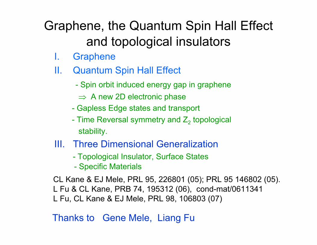
Graphene, the Quantum Spin Hall Effectand topological insulators
I. Graphene II. Quantum Spin Hall Effect
- Spin orbit induced energy gap in graphene⇒ A new 2D electronic phase
- Gapless Edge states and transport- Time Reversal symmetry and Z2 topological
stability.
III. Three Dimensional Generalization- Topological Insulator, Surface States- Specific Materials
CL Kane & EJ Mele, PRL 95, 226801 (05); PRL 95 146802 (05).L Fu & CL Kane, PRB 74, 195312 (06), cond-mat/0611341L Fu, CL Kane & EJ Mele, PRL 98, 106803 (07)
Thanks to Gene Mele, Liang Fu

4 valence electrons in carbon• 3 bonds to neighbors (sp2 σ bonds)
Structural Rigidity within planesWeak Van der Waals attraction between planes
• 1 delocalized π electronElectrical Conductivity
Graphene = A single layer of graphiteA unique 2D electronic material
The Point of a Pencil Graphite
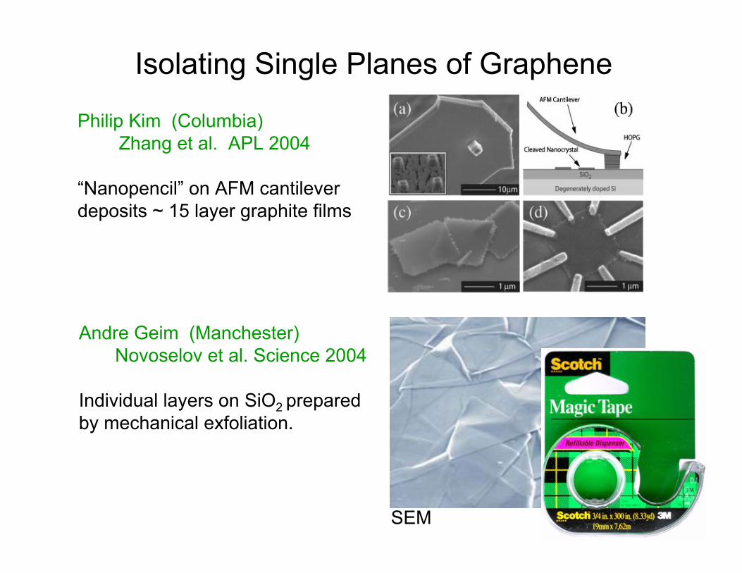
Isolating Single Planes of Graphene
Philip Kim (Columbia) Zhang et al. APL 2004
“Nanopencil” on AFM cantileverdeposits ~ 15 layer graphite films
Andre Geim (Manchester)Novoselov et al. Science 2004
Individual layers on SiO2 prepared by mechanical exfoliation.
SEM
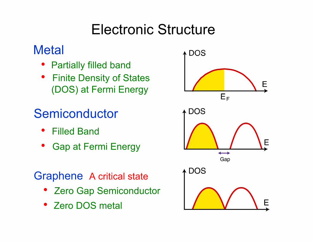
Metal• Partially filled band• Finite Density of States
(DOS) at Fermi Energy
Semiconductor
Graphene A critical state
• Filled Band• Gap at Fermi Energy
Electronic Structure
• Zero Gap Semiconductor• Zero DOS metal
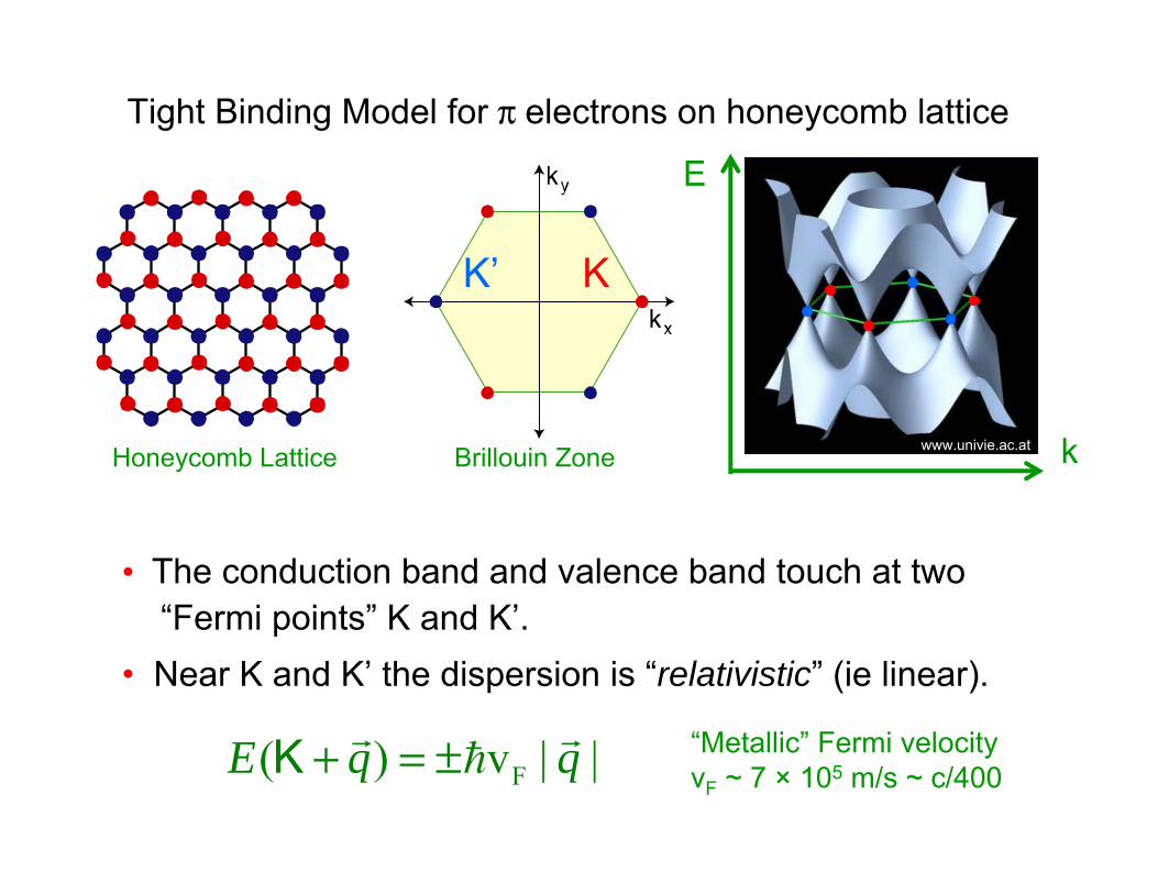
• The conduction band and valence band touch at two “Fermi points” K and K’.
• Near K and K’ the dispersion is “relativistic” (ie linear).
KK’
Tight Binding Model for π electrons on honeycomb lattice
F( ) v | |E q q+ = ±K “Metallic” Fermi velocityvF ~ 7 × 10⁵ m/s ~ c/400
Brillouin ZoneHoneycomb Lattice
E
kwww.univie.ac.at
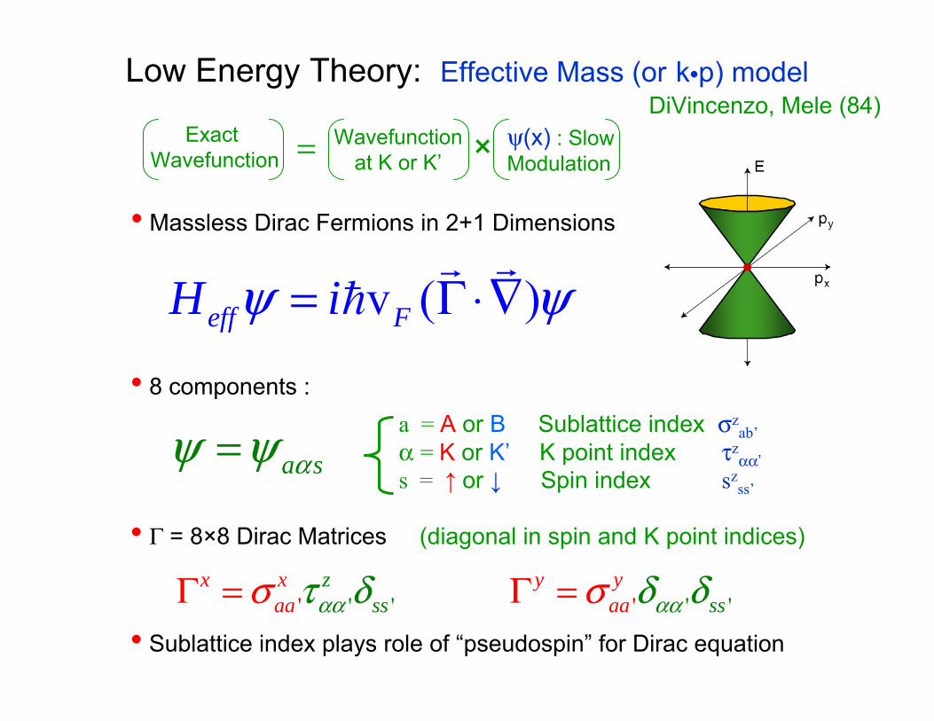
Low Energy Theory: Effective Mass (or kip) modelDiVincenzo, Mele (84)
v ( )eff FH iψ ψ= Γ ⋅∇
a sαψ ψ=• 8 components :
• Γ = 8×8 Dirac Matrices (diagonal in spin and K point indices)
' ' '' ' ' zss s
x x yaa a s
yaαα αατσ δσδ δΓ = Γ =
a = A or B Sublattice index σzab’
α = K or K’ K point index τzαα’
s = ↑ or ↓ Spin index szss’
• Massless Dirac Fermions in 2+1 Dimensions
• Sublattice index plays role of “pseudospin” for Dirac equation
Exact Wavefunction
Wavefunctionat K or K’
ψ(x) : SlowModulation= ×
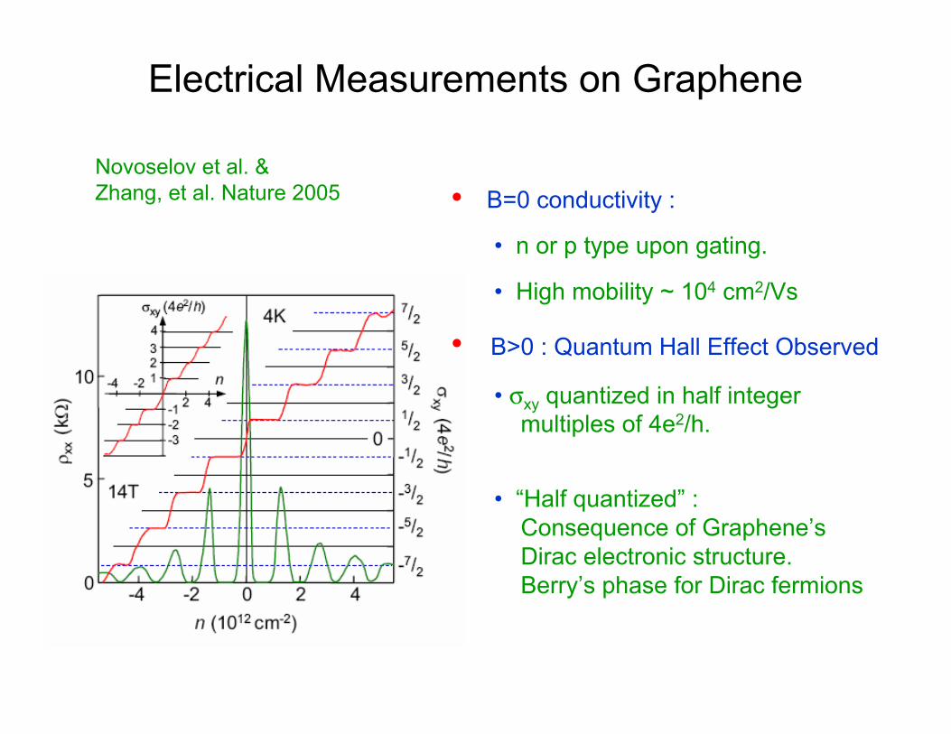
Electrical Measurements on Graphene
Novoselov et al. & Zhang, et al. Nature 2005 • B=0 conductivity :
• n or p type upon gating.
• High mobility ~ 104 cm2/Vs
• B>0 : Quantum Hall Effect Observed
• σxy quantized in half integermultiples of 4e2/h.
• “Half quantized” :Consequence of Graphene’sDirac electronic structure.Berry’s phase for Dirac fermions
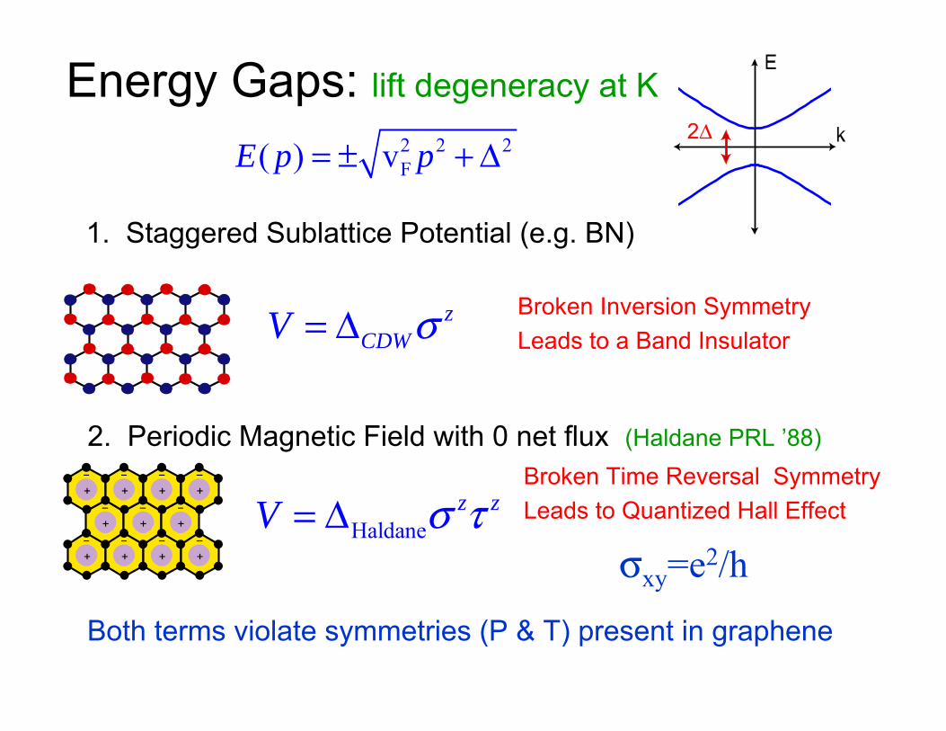
Broken Inversion SymmetryLeads to a Band Insulator
Broken Time Reversal SymmetryLeads to Quantized Hall Effect
σxy=e2/h
2 2 2F( ) vE p p= ± + ∆
zCDWV σ= ∆
Haldanez zV σ τ= ∆
1. Staggered Sublattice Potential (e.g. BN)
2. Periodic Magnetic Field with 0 net flux (Haldane PRL ’88)
2∆
Energy Gaps: lift degeneracy at K
Both terms violate symmetries (P & T) present in graphene
+ + +
+ + + +
+ + + +

Respects ALL symmetries of Graphene, and WILL BE PRESENT. An ideal sheet of graphene has an intrinsic energy gap
z z zSOV sσ τ= ∆
3. Intrinsic Spin Orbit Potential
2∆ p
E
and spins are independent : “ (Haldane)2 ”Leads to Quantum Spin Hall Effect for µ,T << ∆so
ˆ( )2
s sxyJ J J z E
eσ↑ ↓= − = ×
sgn( )2
sxy SO
eσπ
= ∆
2
ˆeJ z Eh
↓↑ = −+ × sJE
J↑
J↓
The spin-orbit energy gap defines a time reversal invariant “topological insulator” phase of matter that is distinct from an ordinary insulator.
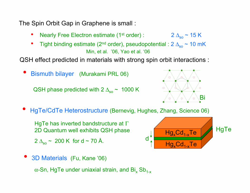
The Spin Orbit Gap in Graphene is small :
• Nearly Free Electron estimate (1st order) : 2 ∆so ~ 15 K• Tight binding estimate (2nd order), pseudopotential : 2 ∆so ~ 10 mK
Min, et al. ’06, Yao et al. ‘06
• Bismuth bilayer (Murakami PRL 06)
QSH effect predicted in materials with strong spin orbit interactions :
Bi
• HgTe/CdTe Heterostructure (Bernevig, Hughes, Zhang, Science 06)
• 3D Materials (Fu, Kane ’06)
α-Sn, HgTe under uniaxial strain, and Bix Sb1-x
HgTe has inverted bandstructure at Γ2D Quantum well exhibits QSH phase
2 ∆so ~ 200 K for d ~ 70 Å.
QSH phase predicted with 2 ∆so ~ 1000 K
HgTe
HgxCd1-xTe
HgxCd1-xTed
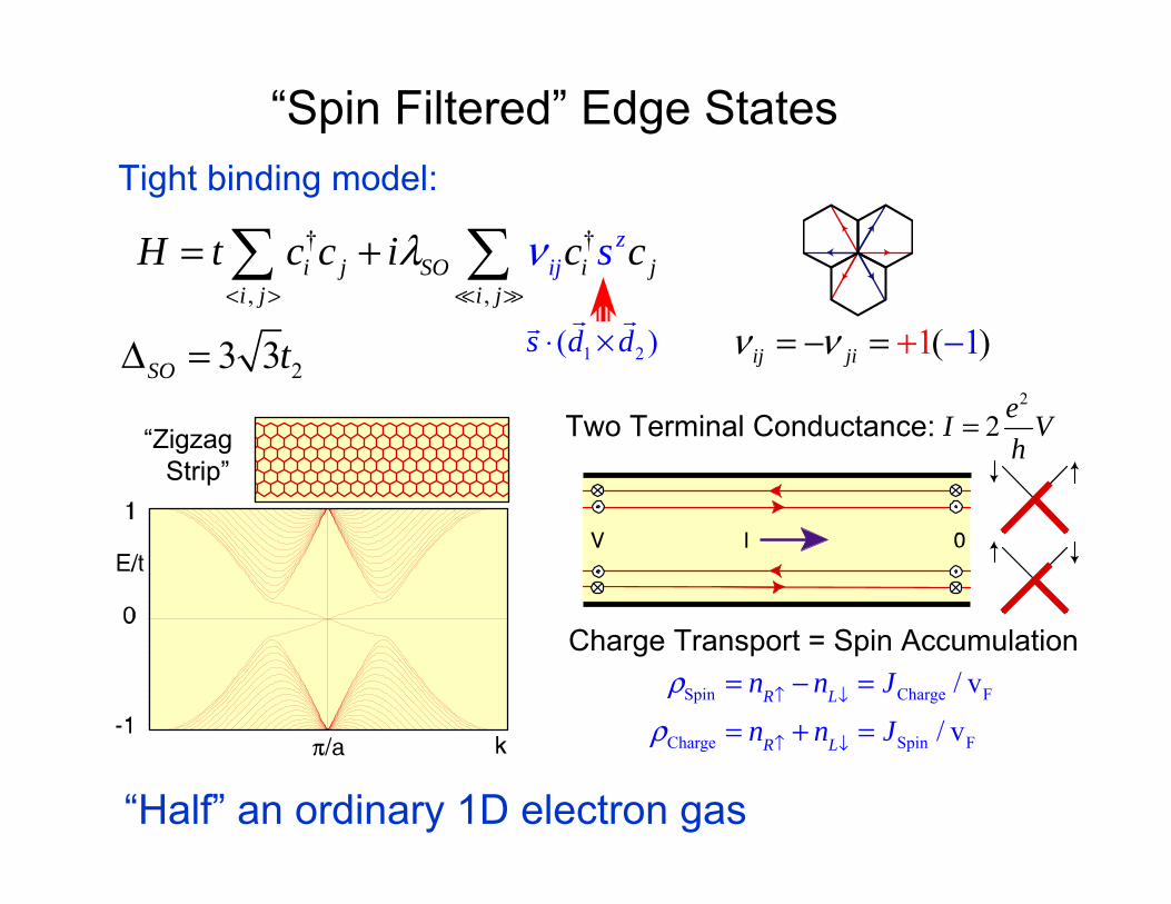
† †
, ,i j SO i j
i j i
zij
jH t c c i c csνλ
< >
= +∑ ∑1 2( )s d d⋅ × 1 1( )ij jiν ν = + −= −
23 3SO t∆ =
“Spin Filtered” Edge States
“Zigzag Strip”
Two Terminal Conductance:2
2 eI Vh
=
Charge Transport = Spin Accumulation
Spin Charge F
Charge Spin F
/ v
/ vR L
R L
n n Jn n J
ρρ
↑ ↓
↑ ↓
= − =
= + =
Tight binding model:
“Half” an ordinary 1D electron gas
Beyond The (Haldane)2 Model
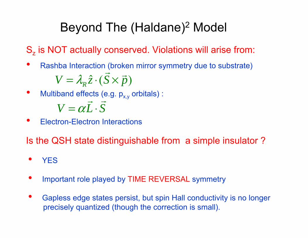
Sz is NOT actually conserved. Violations will arise from:• Rashba Interaction (broken mirror symmetry due to substrate)
• Multiband effects (e.g. px,y orbitals) :
• Electron-Electron InteractionsV L Sα= ⋅
ˆ ( )RV z S pλ= ⋅ ×
Is the QSH state distinguishable from a simple insulator ?
• YES
• Important role played by TIME REVERSAL symmetry
• Gapless edge states persist, but spin Hall conductivity is no longerprecisely quantized (though the correction is small).
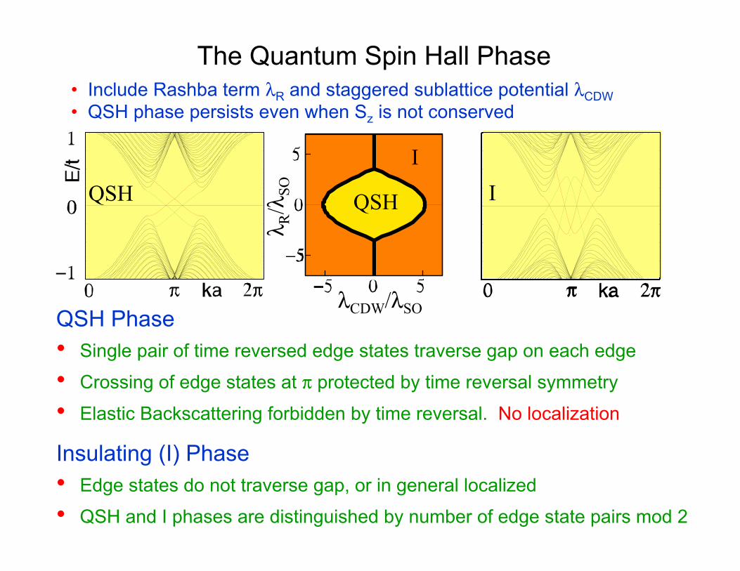
The Quantum Spin Hall Phase
λCDW/λSO
λ R/λ
SO QSH
IQSH I
QSH Phase• Single pair of time reversed edge states traverse gap on each edge
• Crossing of edge states at π protected by time reversal symmetry
• Elastic Backscattering forbidden by time reversal. No localization
Insulating (I) Phase• Edge states do not traverse gap, or in general localized
• QSH and I phases are distinguished by number of edge state pairs mod 2
I
• Include Rashba term λR and staggered sublattice potential λCDW• QSH phase persists even when Sz is not conserved

Topological Invariant• Integer Quantum Hall Effect Thouless, et al. (TKNN) (1982)
Hall conductivity is a Chern invariant, σxy=ne2/h,
• Spin Conserving (Haldane)2 Model- Independent TKNN invariants:- Time Reversal Symmetry : - Spin Hall conductivity :
• Quantum Spin Hall Phase (without spin conservation)- The single defined TKNN integer is ZERO.- QSH phase characterized by a new Z2 invariant protected by time reversal symmetry.
0n n↑ ↓+ =0n n↑ ↓− ≠
21 ( ) ( )2 BZ
n d u uiπ
= ⋅ ∇ × ∇∫ k kk k k
, n n↑ ↓
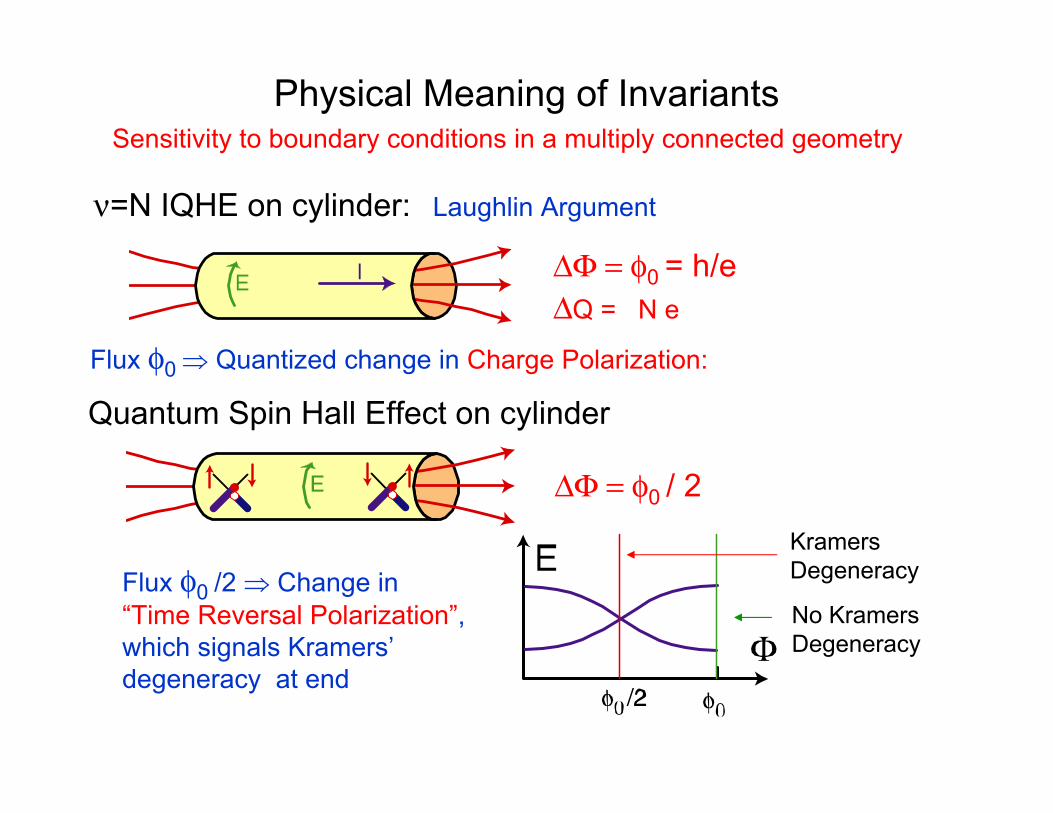
Physical Meaning of Invariants
∆Φ = φ0 = h/e∆Q = N e
Flux φ0 ⇒ Quantized change in Charge Polarization:
ν=N IQHE on cylinder: Laughlin Argument
Quantum Spin Hall Effect on cylinder
∆Φ = φ0 / 2
Flux φ0 /2 ⇒ Change in “Time Reversal Polarization”,which signals Kramers’degeneracy at end
KramersDegeneracy
No KramersDegeneracy
Sensitivity to boundary conditions in a multiply connected geometry

3D Generalization
There are 4 Z2 invariants ν0;(ν1ν2ν3) distinguishing 16 “Topological Insulator” phases.
Fu, Kane & Mele PRL, 106803 (07), cond-mat/0611341Moore & Balents cond-mat/0607314; Roy, cond-mat/0607531
Model system: Distorted diamond lattice with spin orbit interaction
† †1 2
, ,( ) ( )a i i a SO i j
i a i jH t t c c i c s d d cδ λ+= + + ⋅ ×∑ ∑
• δta=0 is a critical point with 3D Dirac points at 3 X points.
• δta (a=1,..,4) opens gaps leading to 8 different TI phases
STIWTI
ν0 = 0, 1 distinguishes “weak” and “strong” topological insulators

I. Weak Topological Insulator ν0 = 0
• Equivalent to layered 2D QSH states (analogous to 3D IQHE states)stacked perpendicular to “mod 2” reciprocal lattice vector (ν1ν2ν3).
• Each surface has either 0 or 2 2D Dirac points.
• Fragile: Disorder eliminates topological distinction.
Electronic structure of a 2D slab :
surface stateswith 2D
Dirac points
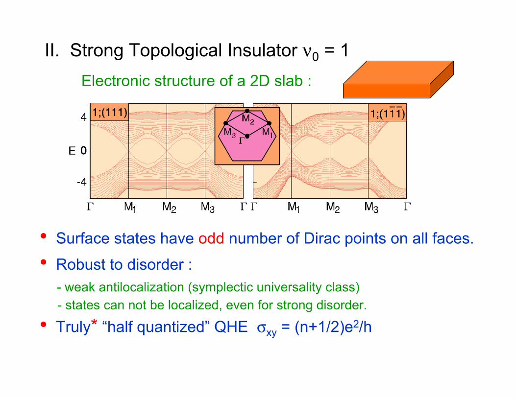
II. Strong Topological Insulator ν0 = 1
• Surface states have odd number of Dirac points on all faces.
• Robust to disorder :- weak antilocalization (symplectic universality class)- states can not be localized, even for strong disorder.
• Truly* “half quantized” QHE σxy = (n+1/2)e2/h
Electronic structure of a 2D slab :
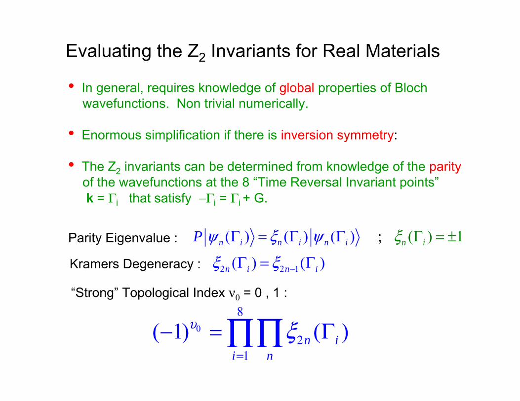
Evaluating the Z2 Invariants for Real Materials
• In general, requires knowledge of global properties of Blochwavefunctions. Non trivial numerically.
• Enormous simplification if there is inversion symmetry:
• The Z2 invariants can be determined from knowledge of the parityof the wavefunctions at the 8 “Time Reversal Invariant points”k = Γi that satisfy −Γi = Γi + G.
Parity Eigenvalue : ; ( ( )) ( ) 1( )n i n i n i n iP ψ ξ ψ ξΓ = ΓΓ = ±Γ
“Strong” Topological Index ν0 = 0 , 1 :
0
8
21
( 1) ( )n ii n
υ ξ=
− = Γ∏∏
Kramers Degeneracy : 2 2 1( ) ( )n i n iξ ξ −Γ = Γ
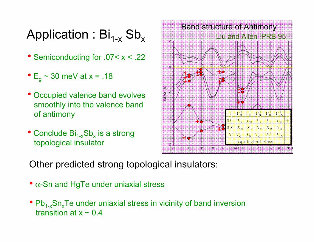
Application : Bi1-x Sbx
• Semiconducting for .07< x < .22
• Eg ~ 30 meV at x = .18
• Occupied valence band evolves smoothly into the valence bandof antimony
• Conclude Bi1-xSbx is a strongtopological insulator
Band structure of AntimonyLiu and Allen PRB 95
Other predicted strong topological insulators:
• α-Sn and HgTe under uniaxial stress
• Pb1-xSnxTe under uniaxial stress in vicinity of band inversiontransition at x ~ 0.4
+
-
+++
-+
--+
+
+
+
-
-
+--

Conclusion• The quantum spin Hall phase shares many similarities with the
quantum Hall effect:
- bulk excitation gap- gapless edge excitations- topological stability- 3D generalization
• But there are also important differences:
- Spin Hall conductivity not quantized (but non zero).- Edge states are not chiral, but “spin filtered”.- Edge transport diffusive (but not localized) at finite T.
• Open Questions :
- Experiments on graphene? bismuth? HgCdTe? 3D materials?- Formulation of Z2 invariant for interacting systems- Effects of disorder on surface states, and critical phenomena
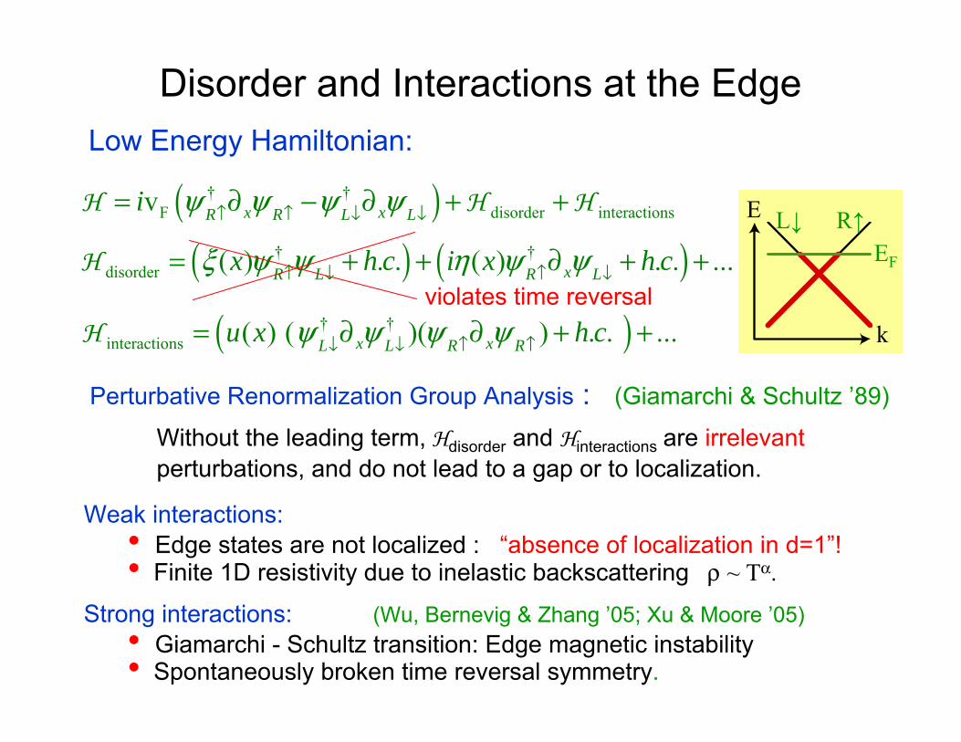
Disorder and Interactions at the Edge
( )† †F disorder interactionsv x xR R L Li ψ ψ ψ ψ↑ ↑ ↓ ↓= ∂ − ∂ + +H H H
Low Energy Hamiltonian:
( ) ( )† †disorder ( ) . . ( ) . . ...xR L R Lx h c i x h cξ ψ ψ η ψ ψ↑ ↓ ↑ ↓= + + ∂ + +H
( )† †interactions ( ) ( )( ) . . ...x xL L R Ru x h cψ ψ ψ ψ↓ ↓ ↑ ↑= ∂ ∂ + +H
Perturbative Renormalization Group Analysis : (Giamarchi & Schultz ’89)
Without the leading term, Hdisorder and Hinteractions are irrelevantperturbations, and do not lead to a gap or to localization.
Weak interactions:• Edge states are not localized : “absence of localization in d=1”!• Finite 1D resistivity due to inelastic backscattering ρ ~ Tα.
Strong interactions: (Wu, Bernevig & Zhang ’05; Xu & Moore ’05)• Giamarchi - Schultz transition: Edge magnetic instability• Spontaneously broken time reversal symmetry.
violates time reversal
EF
R↑L↓
k
E

“Quantum” but not “Quantized”Spin Hall conductance on a cylinder
0he
Φ =
z sxy
d S dGdt dt
Φ=• Rate of spin accumulation on edge:
( ) 0F
sxy z zR L E
eG S Sh
= − ≠• Spin Hall Conductance NOT quantized
emf = ddtΦ−
• For insulator no edge states, or else localized : 0sxyG =
• Spin relaxation rate ~ Inelastic backscattering rate ~ Tα
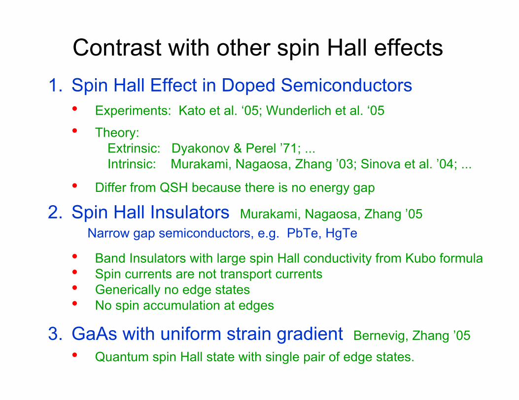
1. Spin Hall Effect in Doped Semiconductors• Experiments: Kato et al. ‘05; Wunderlich et al. ‘05
• Theory: Extrinsic: Dyakonov & Perel ’71; ... Intrinsic: Murakami, Nagaosa, Zhang ’03; Sinova et al. ’04; ...
• Differ from QSH because there is no energy gap
2. Spin Hall Insulators Murakami, Nagaosa, Zhang ’05Narrow gap semiconductors, e.g. PbTe, HgTe
• Band Insulators with large spin Hall conductivity from Kubo formula• Spin currents are not transport currents• Generically no edge states• No spin accumulation at edges
3. GaAs with uniform strain gradient Bernevig, Zhang ’05• Quantum spin Hall state with single pair of edge states.
Contrast with other spin Hall effects


![Quantum Spin Hall Effect and Topological Phase Transition in HgTe … · 2008-02-05 · arXiv:cond-mat/0611399v1 [cond-mat.mes-hall] 15 Nov 2006 Quantum Spin Hall Effect and Topological](https://img.pdfslide.net/doc/110x75/5e5ce054bfcfc250f0532ba9/quantum-spin-hall-effect-and-topological-phase-transition-in-hgte-2008-02-05-arxivcond-mat0611399v1.jpg)