Embed Size (px)
Citation preview
GreenTouch2TM GT208L Capacitive Touch Sensor
v1.1 SPECIFICATION
The Classic of Touch Solution!
www.greenchip.co.kr
The Classic of Touch Solution! GreenChip Inc. Confidential
Product Specification Revised June 2011 v1.1
GreenTouch2TM Series GT208L Capacitive Touch Sensor
2 / 25
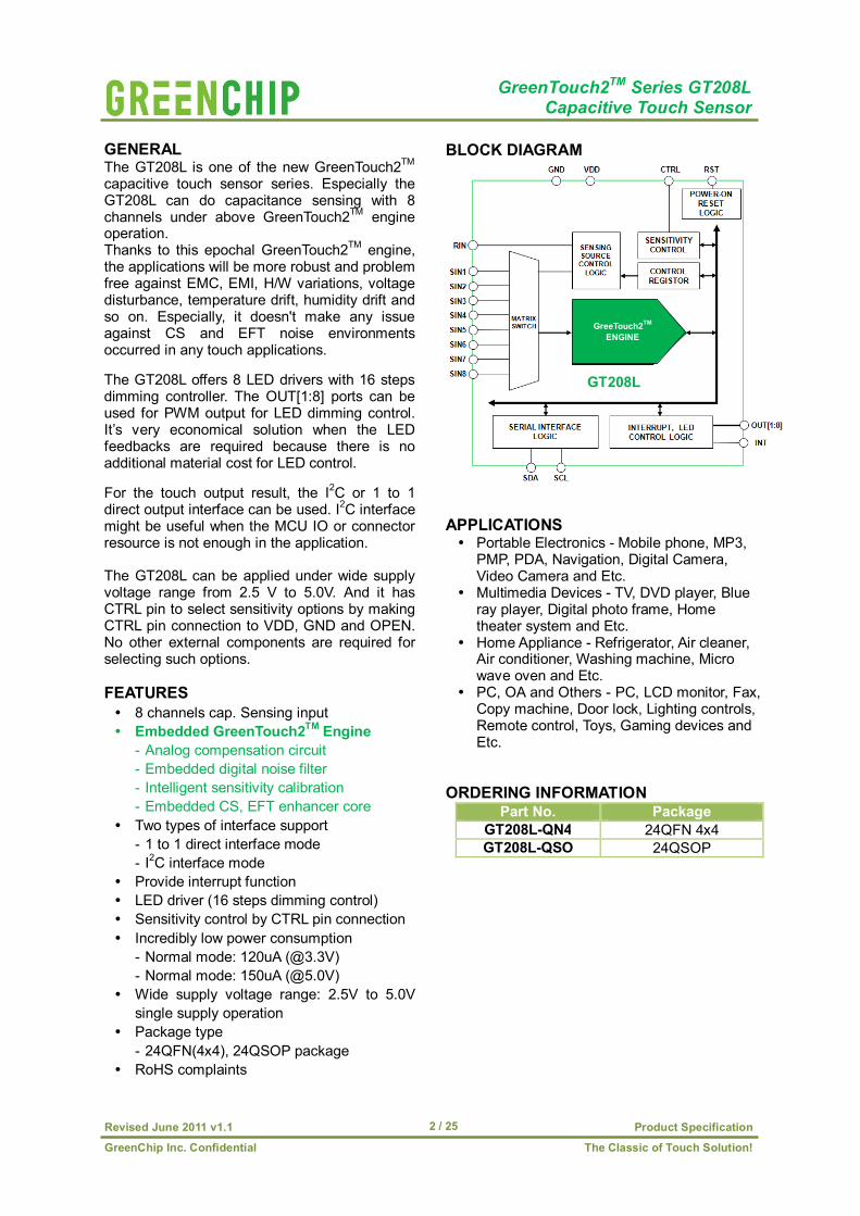
GENERAL The GT208L is one of the new GreenTouch2TM capacitive touch sensor series. Especially the GT208L can do capacitance sensing with 8 channels under above GreenTouch2TM engine operation. Thanks to this epochal GreenTouch2TM engine, the applications will be more robust and problem free against EMC, EMI, H/W variations, voltage disturbance, temperature drift, humidity drift and so on. Especially, it doesn't make any issue against CS and EFT noise environments occurred in any touch applications. The GT208L offers 8 LED drivers with 16 steps dimming controller. The OUT[1:8] ports can be used for PWM output for LED dimming control. It’s very economical solution when the LED feedbacks are required because there is no additional material cost for LED control. For the touch output result, the I2C or 1 to 1 direct output interface can be used. I2C interface might be useful when the MCU IO or connector resource is not enough in the application. The GT208L can be applied under wide supply voltage range from 2.5 V to 5.0V. And it has CTRL pin to select sensitivity options by making CTRL pin connection to VDD, GND and OPEN. No other external components are required for selecting such options. FEATURES 8 channels cap. Sensing input Embedded GreenTouch2TM Engine
- Analog compensation circuit - Embedded digital noise filter - Intelligent sensitivity calibration - Embedded CS, EFT enhancer core
Two types of interface support - 1 to 1 direct interface mode - I2C interface mode
Provide interrupt function LED driver (16 steps dimming control) Sensitivity control by CTRL pin connection Incredibly low power consumption
- Normal mode: 120uA (@3.3V) - Normal mode: 150uA (@5.0V)
Wide supply voltage range: 2.5V to 5.0V single supply operation
Package type - 24QFN(4x4), 24QSOP package
RoHS complaints
BLOCK DIAGRAM
APPLICATIONS Portable Electronics - Mobile phone, MP3,
PMP, PDA, Navigation, Digital Camera, Video Camera and Etc.
Multimedia Devices - TV, DVD player, Blue ray player, Digital photo frame, Home theater system and Etc.
Home Appliance - Refrigerator, Air cleaner, Air conditioner, Washing machine, Micro wave oven and Etc.
PC, OA and Others - PC, LCD monitor, Fax, Copy machine, Door lock, Lighting controls, Remote control, Toys, Gaming devices and Etc.
ORDERING INFORMATION
Part No. Package GT208L-QN4 24QFN 4x4 GT208L-QSO 24QSOP
GT208L
GreeTouch2TM ENGINE
The Classic of Touch Solution! GreenChip Inc. Confidential
Product Specification Revised June 2011 v1.1
GreenTouch2TM Series GT208L Capacitive Touch Sensor
3 / 25
REVISION HISTORY
Version Date Revision Contents v1.0 May 2011 Release version V1.1 June 2011 Edit 3-7 CTRL Pin selection ( CHIP ID )
Edit Description of SEN_IDLE_TIME in 4-3-8 General3 Control Registers
Copyright © 2009 by GreenChip Inc. - All Rights RESERVE.
GreenChip owns all right, title and interest in the property and products described herein, unless otherwise indicated. No part of this document may be translated to another language or produced or transmitted in any form
or by any information storage and retrieval system without written permission from GreenChip. GreenChip reserves the right to change products and specifications without written notice. Customers are
advised to obtain the latest versions of any product specifications.
GREENCHIP MAKES NO WARRANTIES, EXPRESSED OR IMPLIED, OF MERCHANTABILITY OR FITNESS FOR A PARTICULAR PURPOSE, OTHER THAN COMPLIANCE WITH THE APPLICABLE GREENCHIP
SPECIFICATION SHEET FOR THE PRODUCT AT THE TIME OF DELIVERY. IN NO EVENT SHALL GREENCHIP BE LIABLE FOR ANY INDIRECT, INCIDENTAL OR CONSEQUENTIAL DAMAGES AS A RESULT
OF THE PRODUCT’S PERFORMANCE OR FAILURE TO MEET ANY ASPECT OF SUCH SPECIFICATION. GREENCHIP PRODUCTS ARE NOT DESIGNED OR INTENDED FOR USE IN LIFE SUPPORT APPLIANCES,
DEVICES OR SYSTEMS WHERE A MALFUNCTION OF A GREENCHIP DEVICE COULD RESULT IN A PERSONAL INJURY OR LOSS OF LIFE. CUSTOMERS USING OR SELLING GREENCHIP DEVICES FOR
USE IN SUCH APPLICATIONS DO SO AT THEIR OWN RISK AND AGREE TO FULLY INDEMNIFY GREENCHIP FOR ANY DAMAGES RESULTING FROM SUCH IMPROPER USE OR SALE.
Information contained herein is presented only as a guide for the applications of our products. GreenChip does
not warrant this product to be free of claims of patent infringement by any third party and disclaims any warranty or indemnification against patent infringement. No responsibility is assumed by GreenChip for any patent infringement resulting from use of its products by themselves or in combination with any other products. No license is hereby granted by implication or otherwise under any patent or patent rights of GreenChip.
The GreenChip logo is a registered trademark of GreenChip.
www.greenchip.co.kr
The Classic of Touch Solution! GreenChip Inc. Confidential
Product Specification Revised June 2011 v1.1
GreenTouch2TM Series GT208L Capacitive Touch Sensor
4 / 25
GENERAL -------------------------------------------------------------------------------------------------------------------- 2 FEATURES ------------------------------------------------------------------------------------------------------------------ 2 BLOCK DIAGRAM --------------------------------------------------------------------------------------------------------- 2 APPLICATIONS ------------------------------------------------------------------------------------------------------------ 2 ORDERING INFORAMTION -------------------------------------------------------------------------------------------- 2 REVISION HISTORY ------------------------------------------------------------------------------------------------------ 3 Chapter 1: Pinout Information
1-1 24 QFN Pinout --------------------------------------------------------------------------------------------------- 5 1-2 24 QSOP Pinout ------------------------------------------------------------------------------------------------- 6
Chapter 2: Electrical Specification
2-1 Absolute Maximum Ratings ---------------------------------------------------------------------------------- 7 2-2 DC & Operating Characteristics ----------------------------------------------------------------------------- 7 2-3 ESD & Latch-Up Characteristics ---------------------------------------------------------------------------- 8 2-4 I2C Interface Timing Characteristics ------------------------------------------------------------------------ 9
Chapter 3: Functional Description
3-1 Reset and Operation Modes -------------------------------------------------------------------------------- 10 3-2 Implementation of Sensing & Reference Inputs -------------------------------------------------------- 11 3-3 LED PWM Drive ------------------------------------------------------------------------------------------------ 12 3-4 1 to 1 Direct Output Interfaces ------------------------------------------------------------------------------ 12 3-5 I2C Interface ----------------------------------------------------------------------------------------------------- 13 3-6 Interrupt Output ------------------------------------------------------------------------------------------------- 14 3-7 CTRL Pin Selection -------------------------------------------------------------------------------------------- 14
Chapter 4: Register Description
4-1 I2C Write and Read Operation ------------------------------------------------------------------------------ 15 4-2 Register Map ---------------------------------------------------------------------------------------------------- 16 4-3 Register Description ------------------------------------------------------------------------------------------- 17
Chapter 5: Application Notes
5-1 Application Circuit Example --------------------------------------------------------------------------------- 21 5-2 Application Notes ---------------------------------------------------------------------------------------------- 22
Chapter 6: Package Information
6-1 Package Outside Drawings for GT208L-QN4 ---------------------------------------------------------- 24 6-2 Package Outside Drawings for GT208L-QSO ---------------------------------------------------------- 25
Contents
The Classic of Touch Solution! GreenChip Inc. Confidential
Product Specification Revised June 2011 v1.1 5 / 25
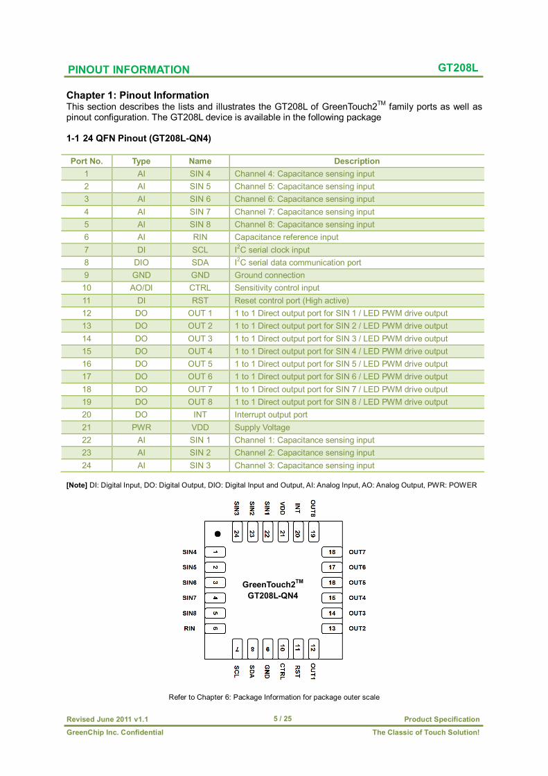
GT208L Chapter 1: Pinout Information This section describes the lists and illustrates the GT208L of GreenTouch2TM family ports as well as pinout configuration. The GT208L device is available in the following package 1-1 24 QFN Pinout (GT208L-QN4) Port No. Type Name Description
1 AI SIN 4 Channel 4: Capacitance sensing input 2 AI SIN 5 Channel 5: Capacitance sensing input 3 AI SIN 6 Channel 6: Capacitance sensing input 4 AI SIN 7 Channel 7: Capacitance sensing input 5 AI SIN 8 Channel 8: Capacitance sensing input 6 AI RIN Capacitance reference input 7 DI SCL I2C serial clock input 8 DIO SDA I2C serial data communication port 9 GND GND Ground connection 10 AO/DI CTRL Sensitivity control input 11 DI RST Reset control port (High active) 12 DO OUT 1 1 to 1 Direct output port for SIN 1 / LED PWM drive output 13 DO OUT 2 1 to 1 Direct output port for SIN 2 / LED PWM drive output 14 DO OUT 3 1 to 1 Direct output port for SIN 3 / LED PWM drive output 15 DO OUT 4 1 to 1 Direct output port for SIN 4 / LED PWM drive output 16 DO OUT 5 1 to 1 Direct output port for SIN 5 / LED PWM drive output 17 DO OUT 6 1 to 1 Direct output port for SIN 6 / LED PWM drive output 18 DO OUT 7 1 to 1 Direct output port for SIN 7 / LED PWM drive output 19 DO OUT 8 1 to 1 Direct output port for SIN 8 / LED PWM drive output 20 DO INT Interrupt output port 21 PWR VDD Supply Voltage 22 AI SIN 1 Channel 1: Capacitance sensing input 23 AI SIN 2 Channel 2: Capacitance sensing input 24 AI SIN 3 Channel 3: Capacitance sensing input
[Note] DI: Digital Input, DO: Digital Output, DIO: Digital Input and Output, AI: Analog Input, AO: Analog Output, PWR: POWER
Refer to Chapter 6: Package Information for package outer scale
PINOUT INFORMATION
GreenTouch2TM
GT208L-QN4
The Classic of Touch Solution! GreenChip Inc. Confidential
Product Specification Revised June 2011 v1.1 6 / 25
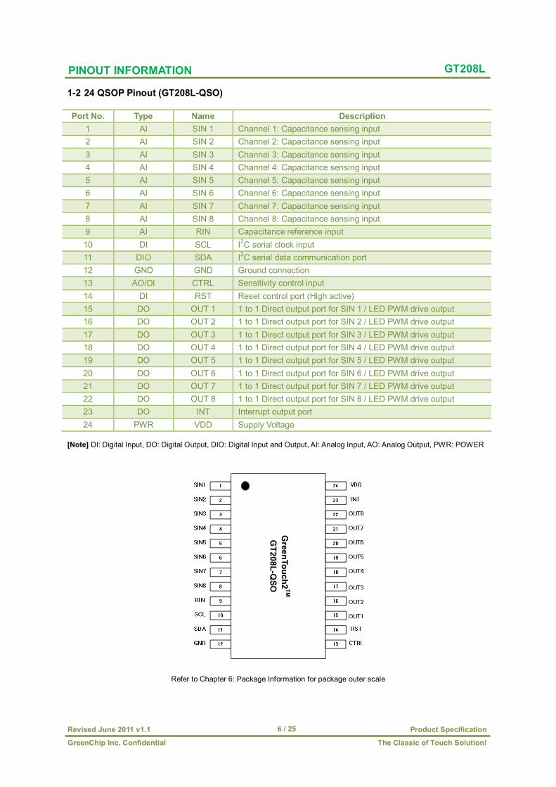
GT208L 1-2 24 QSOP Pinout (GT208L-QSO) Port No. Type Name Description
1 AI SIN 1 Channel 1: Capacitance sensing input 2 AI SIN 2 Channel 2: Capacitance sensing input 3 AI SIN 3 Channel 3: Capacitance sensing input 4 AI SIN 4 Channel 4: Capacitance sensing input 5 AI SIN 5 Channel 5: Capacitance sensing input 6 AI SIN 6 Channel 6: Capacitance sensing input 7 AI SIN 7 Channel 7: Capacitance sensing input 8 AI SIN 8 Channel 8: Capacitance sensing input 9 AI RIN Capacitance reference input 10 DI SCL I2C serial clock input 11 DIO SDA I2C serial data communication port 12 GND GND Ground connection 13 AO/DI CTRL Sensitivity control input 14 DI RST Reset control port (High active) 15 DO OUT 1 1 to 1 Direct output port for SIN 1 / LED PWM drive output 16 DO OUT 2 1 to 1 Direct output port for SIN 2 / LED PWM drive output 17 DO OUT 3 1 to 1 Direct output port for SIN 3 / LED PWM drive output 18 DO OUT 4 1 to 1 Direct output port for SIN 4 / LED PWM drive output 19 DO OUT 5 1 to 1 Direct output port for SIN 5 / LED PWM drive output 20 DO OUT 6 1 to 1 Direct output port for SIN 6 / LED PWM drive output 21 DO OUT 7 1 to 1 Direct output port for SIN 7 / LED PWM drive output 22 DO OUT 8 1 to 1 Direct output port for SIN 8 / LED PWM drive output 23 DO INT Interrupt output port 24 PWR VDD Supply Voltage
[Note] DI: Digital Input, DO: Digital Output, DIO: Digital Input and Output, AI: Analog Input, AO: Analog Output, PWR: POWER
Refer to Chapter 6: Package Information for package outer scale
PINOUT INFORMATION
GreenTouch2
TM G
T208L-QSO
The Classic of Touch Solution! GreenChip Inc. Confidential
Product Specification Revised June 2011 v1.1 7 / 25
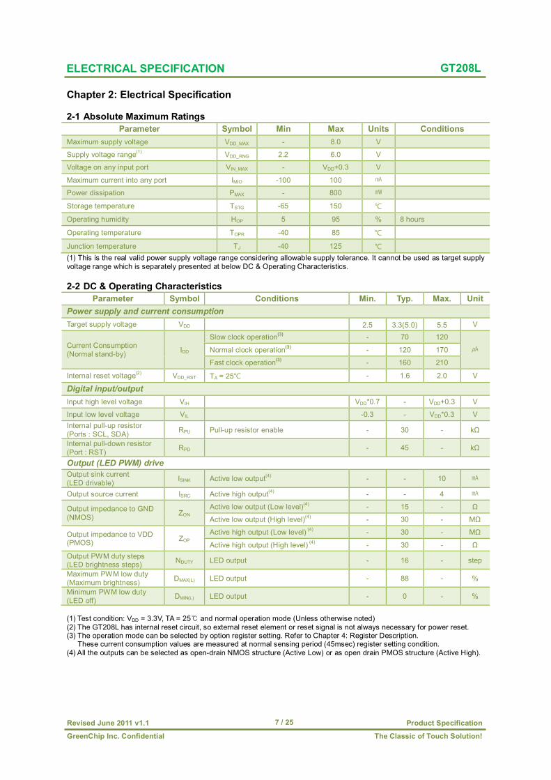
GT208L Chapter 2: Electrical Specification 2-1 Absolute Maximum Ratings
Parameter Symbol Min Max Units Conditions Maximum supply voltage VDD_MAX - 8.0 V
Supply voltage range(1) VDD_RNG 2.2 6.0 V
Voltage on any input port VIN_MAX - VDD+0.3 V
Maximum current into any port IMIO -100 100 ㎃
Power dissipation PMAX - 800 ㎽
Storage temperature TSTG -65 150 ℃
Operating humidity HOP 5 95 % 8 hours
Operating temperature TOPR -40 85 ℃
Junction temperature TJ -40 125 ℃ (1) This is the real valid power supply voltage range considering allowable supply tolerance. It cannot be used as target supply voltage range which is separately presented at below DC & Operating Characteristics. 2-2 DC & Operating Characteristics
Parameter Symbol Conditions Min. Typ. Max. Unit Power supply and current consumption Target supply voltage VDD 2.5 3.3(5.0) 5.5 V
Current Consumption (Normal stand-by) IDD
Slow clock operation(3) - 70 120
㎂ Normal clock operation(3) - 120 170
Fast clock operation(3) - 160 210
Internal reset voltage(2) VDD_RST TA = 25℃ - 1.6 2.0 V
Digital input/output Input high level voltage VIH VDD*0.7 - VDD+0.3 V
Input low level voltage VIL -0.3 - VDD*0.3 V Internal pull-up resistor (Ports : SCL, SDA) RPU Pull-up resistor enable - 30 - kΩ
Internal pull-down resistor (Port : RST) RPD - 45 - kΩ
Output (LED PWM) drive Output sink current (LED drivable) ISINK Active low output(4) - - 10 ㎃
Output source current ISRC Active high output(4) - - 4 ㎃
Output impedance to GND (NMOS) ZON
Active low output (Low level)(4) - 15 - Ω
Active low output (High level)(4) - 30 - MΩ
Output impedance to VDD (PMOS) ZOP
Active high output (Low level) (4) - 30 - MΩ
Active high output (High level) (4) - 30 - Ω Output PWM duty steps (LED brightness steps) NDUTY LED output - 16 - step
Maximum PWM low duty (Maximum brightness) DMAX(L) LED output - 88 - %
Minimum PWM low duty (LED off) DMIN(L) LED output - 0 - %
(1) Test condition: VDD = 3.3V, TA = 25 and normal operation mode (Unless otherwise noted)℃ (2) The GT208L has internal reset circuit, so external reset element or reset signal is not always necessary for power reset. (3) The operation mode can be selected by option register setting. Refer to Chapter 4: Register Description. These current consumption values are measured at normal sensing period (45msec) register setting condition. (4) All the outputs can be selected as open-drain NMOS structure (Active Low) or as open drain PMOS structure (Active High).
ELECTRICAL SPECIFICATION
The Classic of Touch Solution! GreenChip Inc. Confidential
Product Specification Revised June 2011 v1.1 8 / 25
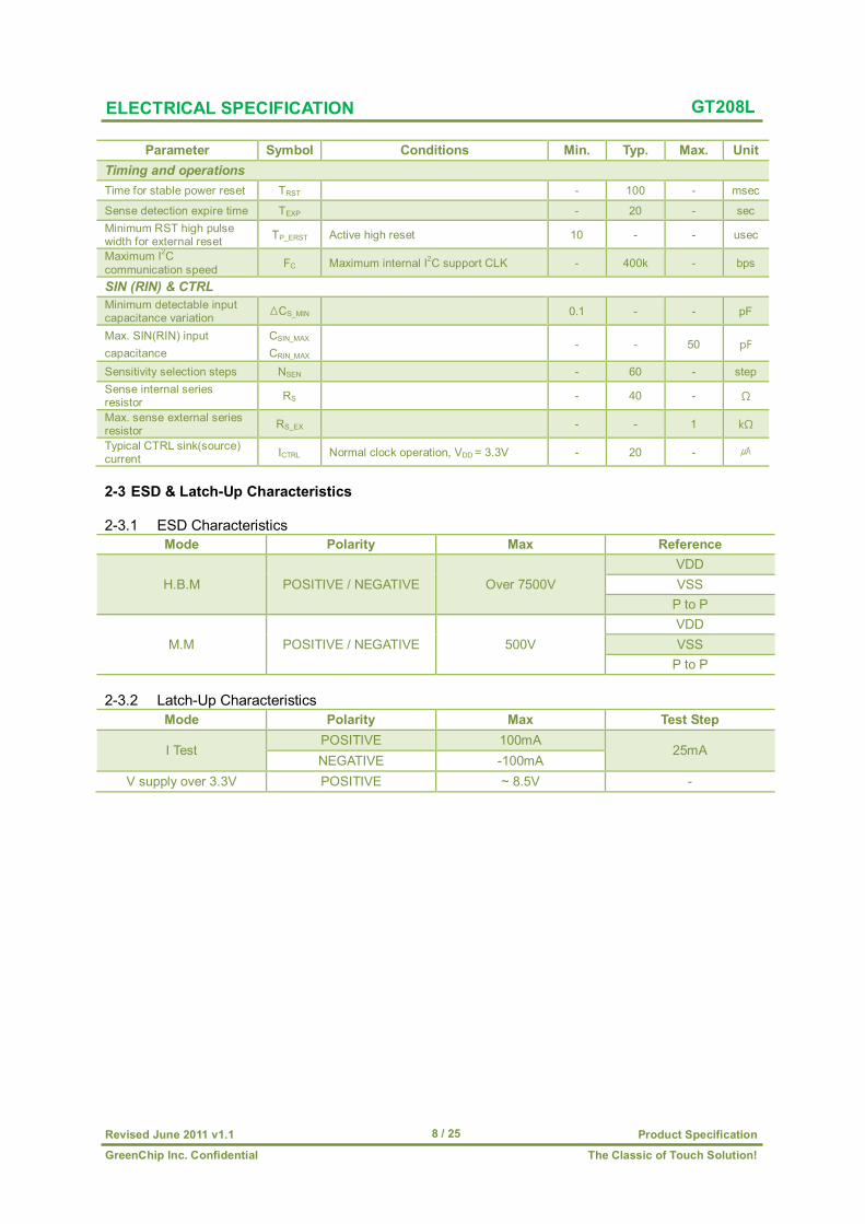
GT208L
Parameter Symbol Conditions Min. Typ. Max. Unit Timing and operations Time for stable power reset TRST - 100 - msec
Sense detection expire time TEXP - 20 - sec Minimum RST high pulse width for external reset TP_ERST Active high reset 10 - - usec
Maximum I2C communication speed FC Maximum internal I2C support CLK - 400k - bps
SIN (RIN) & CTRL Minimum detectable input capacitance variation ΔCS_MIN 0.1 - - pF
Max. SIN(RIN) input capacitance
CSIN_MAX
CRIN_MAX - - 50 pF
Sensitivity selection steps NSEN - 60 - step Sense internal series resistor RS - 40 - Ω
Max. sense external series resistor RS_EX - - 1 kΩ
Typical CTRL sink(source) current ICTRL Normal clock operation, VDD = 3.3V - 20 - ㎂
2-3 ESD & Latch-Up Characteristics
2-3.1 ESD Characteristics
Mode Polarity Max Reference
H.B.M POSITIVE / NEGATIVE Over 7500V VDD VSS
P to P
M.M POSITIVE / NEGATIVE 500V VDD VSS
P to P 2-3.2 Latch-Up Characteristics
Mode Polarity Max Test Step
I Test POSITIVE 100mA
25mA NEGATIVE -100mA
V supply over 3.3V POSITIVE ~ 8.5V -
ELECTRICAL SPECIFICATION
The Classic of Touch Solution! GreenChip Inc. Confidential
Product Specification Revised June 2011 v1.1 9 / 25
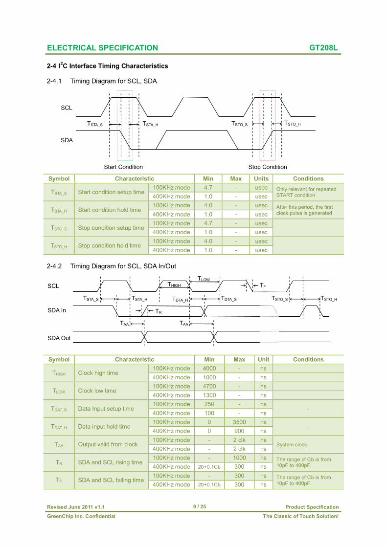
GT208L 2-4 I2C Interface Timing Characteristics 2-4.1 Timing Diagram for SCL, SDA
Symbol Characteristic Min Max Units Conditions
TSTA_S Start condition setup time 100KHz mode 4.7 - usec Only relevant for repeated
START condition 400KHz mode 1.0 - usec
TSTA_H Start condition hold time 100KHz mode 4.0 - usec After this period, the first
clock pulse is generated 400KHz mode 1.0 - usec
TSTO_S Stop condition setup time 100KHz mode 4.7 - usec
400KHz mode 1.0 - usec
TSTO_H Stop condition hold time 100KHz mode 4.0 - usec
400KHz mode 1.0 - usec
2-4.2 Timing Diagram for SCL, SDA In/Out
Symbol Characteristic Min Max Unit Conditions
THIGH Clock high time 100KHz mode 4000 - ns
400KHz mode 1000 - ns
TLOW Clock low time 100KHz mode 4700 - ns
400KHz mode 1300 - ns
TDAT_S Data Input setup time 100KHz mode 250 - ns
- 400KHz mode 100 - ns
TDAT_H Data input hold time 100KHz mode 0 3500 ns
- 400KHz mode 0 900 ns
TAA Output valid from clock 100KHz mode - 2 clk ns
System clock 400KHz mode - 2 clk ns
TR SDA and SCL rising time 100KHz mode - 1000 ns The range of Cb is from
10pF to 400pF. 400KHz mode 20+0.1Cb 300 ns
TF SDA and SCL falling time 100KHz mode - 300 ns The range of Cb is from
10pF to 400pF. 400KHz mode 20+0.1Cb 300 ns
SCL THIGH
SDA In
SDA Out
TLOW TF
TR
TSTA_S TSTA_H
TAA TAA
TDTA_H TDTA_S TSTO_S TSTO_H
SCL
SDA
Start Condition Stop Condition
TSTA_S TSTA_H TSTO_H TSTO_S
ELECTRICAL SPECIFICATION
The Classic of Touch Solution! GreenChip Inc. Confidential
Product Specification Revised June 2011 v1.1 10 / 25
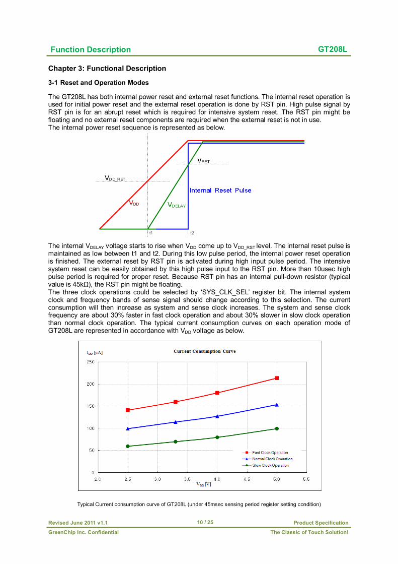
GT208L Chapter 3: Functional Description 3-1 Reset and Operation Modes The GT208L has both internal power reset and external reset functions. The internal reset operation is used for initial power reset and the external reset operation is done by RST pin. High pulse signal by RST pin is for an abrupt reset which is required for intensive system reset. The RST pin might be floating and no external reset components are required when the external reset is not in use. The internal power reset sequence is represented as below.
The internal VDELAY voltage starts to rise when VDD come up to VDD_RST level. The internal reset pulse is maintained as low between t1 and t2. During this low pulse period, the internal power reset operation is finished. The external reset by RST pin is activated during high input pulse period. The intensive system reset can be easily obtained by this high pulse input to the RST pin. More than 10usec high pulse period is required for proper reset. Because RST pin has an internal pull-down resistor (typical value is 45kΩ), the RST pin might be floating. The three clock operations could be selected by ‘SYS_CLK_SEL’ register bit. The internal system clock and frequency bands of sense signal should change according to this selection. The current consumption will then increase as system and sense clock increases. The system and sense clock frequency are about 30% faster in fast clock operation and about 30% slower in slow clock operation than normal clock operation. The typical current consumption curves on each operation mode of GT208L are represented in accordance with VDD voltage as below.
Typical Current consumption curve of GT208L (under 45msec sensing period register setting condition)
Function Description
The Classic of Touch Solution! GreenChip Inc. Confidential
Product Specification Revised June 2011 v1.1 11 / 25
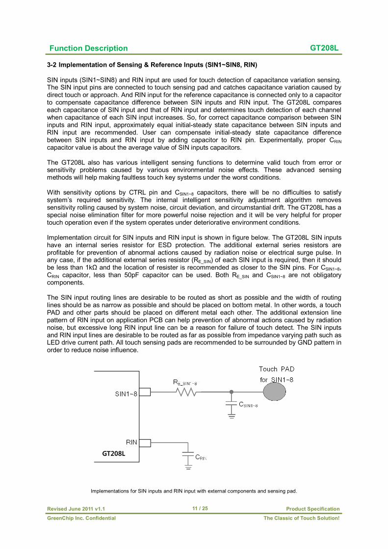
GT208L 3-2 Implementation of Sensing & Reference Inputs (SIN1~SIN8, RIN) SIN inputs (SIN1~SIN8) and RIN input are used for touch detection of capacitance variation sensing. The SIN input pins are connected to touch sensing pad and catches capacitance variation caused by direct touch or approach. And RIN input for the reference capacitance is connected only to a capacitor to compensate capacitance difference between SIN inputs and RIN input. The GT208L compares each capacitance of SIN input and that of RIN input and determines touch detection of each channel when capacitance of each SIN input increases. So, for correct capacitance comparison between SIN inputs and RIN input, approximately equal initial-steady state capacitance between SIN inputs and RIN input are recommended. User can compensate initial-steady state capacitance difference between SIN inputs and RIN input by adding capacitor to RIN pin. Experimentally, proper CRIN capacitor value is about the average value of SIN inputs capacitors. The GT208L also has various intelligent sensing functions to determine valid touch from error or sensitivity problems caused by various environmental noise effects. These advanced sensing methods will help making faultless touch key systems under the worst conditions. With sensitivity options by CTRL pin and CSIN1~8 capacitors, there will be no difficulties to satisfy system’s required sensitivity. The internal intelligent sensitivity adjustment algorithm removes sensitivity rolling caused by system noise, circuit deviation, and circumstantial drift. The GT208L has a special noise elimination filter for more powerful noise rejection and it will be very helpful for proper touch operation even if the system operates under deteriorative environment conditions. Implementation circuit for SIN inputs and RIN input is shown in figure below. The GT208L SIN inputs have an internal series resistor for ESD protection. The additional external series resistors are profitable for prevention of abnormal actions caused by radiation noise or electrical surge pulse. In any case, if the additional external series resistor (RE_SIN) of each SIN input is required, then it should be less than 1kΩ and the location of resister is recommended as closer to the SIN pins. For CSIN1~8, CRIN capacitor, less than 50pF capacitor can be used. Both RE_SIN and CSIN1~8 are not obligatory components. The SIN input routing lines are desirable to be routed as short as possible and the width of routing lines should be as narrow as possible and should be placed on bottom metal. In other words, a touch PAD and other parts should be placed on different metal each other. The additional extension line pattern of RIN input on application PCB can help prevention of abnormal actions caused by radiation noise, but excessive long RIN input line can be a reason for failure of touch detect. The SIN inputs and RIN input lines are desirable to be routed as far as possible from impedance varying path such as LED drive current path. All touch sensing pads are recommended to be surrounded by GND pattern in order to reduce noise influence.
Implementations for SIN inputs and RIN input with external components and sensing pad.
Function Description
GT208L
The Classic of Touch Solution! GreenChip Inc. Confidential
Product Specification Revised June 2011 v1.1 12 / 25
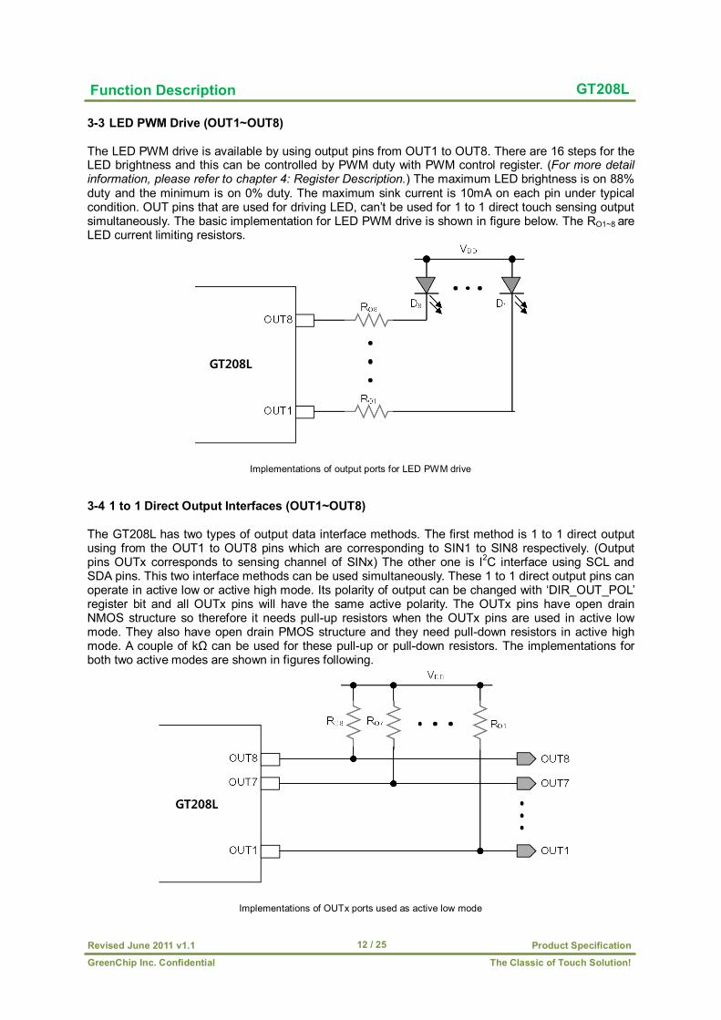
GT208L 3-3 LED PWM Drive (OUT1~OUT8) The LED PWM drive is available by using output pins from OUT1 to OUT8. There are 16 steps for the LED brightness and this can be controlled by PWM duty with PWM control register. (For more detail information, please refer to chapter 4: Register Description.) The maximum LED brightness is on 88% duty and the minimum is on 0% duty. The maximum sink current is 10mA on each pin under typical condition. OUT pins that are used for driving LED, can’t be used for 1 to 1 direct touch sensing output simultaneously. The basic implementation for LED PWM drive is shown in figure below. The RO1~8 are LED current limiting resistors.
Implementations of output ports for LED PWM drive
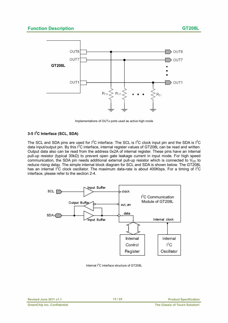
3-4 1 to 1 Direct Output Interfaces (OUT1~OUT8) The GT208L has two types of output data interface methods. The first method is 1 to 1 direct output using from the OUT1 to OUT8 pins which are corresponding to SIN1 to SIN8 respectively. (Output pins OUTx corresponds to sensing channel of SINx) The other one is I2C interface using SCL and SDA pins. This two interface methods can be used simultaneously. These 1 to 1 direct output pins can operate in active low or active high mode. Its polarity of output can be changed with ‘DIR_OUT_POL’ register bit and all OUTx pins will have the same active polarity. The OUTx pins have open drain NMOS structure so therefore it needs pull-up resistors when the OUTx pins are used in active low mode. They also have open drain PMOS structure and they need pull-down resistors in active high mode. A couple of kΩ can be used for these pull-up or pull-down resistors. The implementations for both two active modes are shown in figures following.
Implementations of OUTx ports used as active low mode
Function Description
GT208L
GT208L
The Classic of Touch Solution! GreenChip Inc. Confidential
Product Specification Revised June 2011 v1.1 13 / 25
GT208L
Implementations of OUTx ports used as active high mode 3-5 I2C Interface (SCL, SDA) The SCL and SDA pins are used for I2C interface. The SCL is I2C clock input pin and the SDA is I2C data input/output pin. By this I2C interface, internal register values of GT208L can be read and written. Output data also can be read from the address 0x2A of internal register. These pins have an internal pull-up resistor (typical 30kΩ) to prevent open gate leakage current in input mode. For high speed communication, the SDA pin needs additional external pull-up resistor which is connected to VDD to reduce rising delay. The simple internal block diagram for SCL and SDA is shown below. The GT208L has an internal I2C clock oscillator. The maximum data-rate is about 400Kbps. For a timing of I2C interface, please refer to the section 2-4.
Internal I2C interface structure of GT208L
Function Description
I2C Communication Module of GT208L
GT208L
The Classic of Touch Solution! GreenChip Inc. Confidential
Product Specification Revised June 2011 v1.1 14 / 25
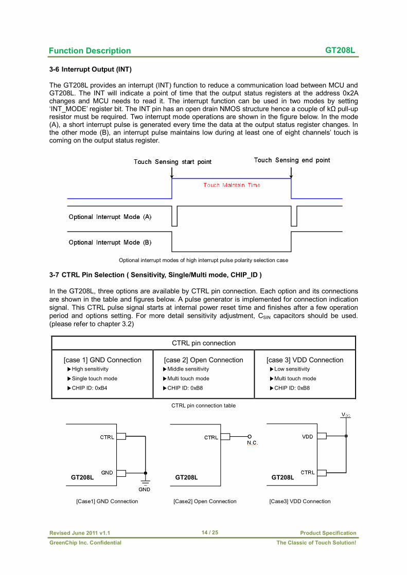
GT208L 3-6 Interrupt Output (INT) The GT208L provides an interrupt (INT) function to reduce a communication load between MCU and GT208L. The INT will indicate a point of time that the output status registers at the address 0x2A changes and MCU needs to read it. The interrupt function can be used in two modes by setting ‘INT_MODE’ register bit. The INT pin has an open drain NMOS structure hence a couple of kΩ pull-up resistor must be required. Two interrupt mode operations are shown in the figure below. In the mode (A), a short interrupt pulse is generated every time the data at the output status register changes. In the other mode (B), an interrupt pulse maintains low during at least one of eight channels’ touch is coming on the output status register.
Optional interrupt modes of high interrupt pulse polarity selection case
3-7 CTRL Pin Selection ( Sensitivity, Single/Multi mode, CHIP_ID )
In the GT208L, three options are available by CTRL pin connection. Each option and its connections are shown in the table and figures below. A pulse generator is implemented for connection indication signal. This CTRL pulse signal starts at internal power reset time and finishes after a few operation period and options setting. For more detail sensitivity adjustment, CSIN capacitors should be used. (please refer to chapter 3.2)
CTRL pin connection
[case 1] GND Connection ▶High sensitivity
▶Single touch mode
▶CHIP ID: 0xB4
[case 2] Open Connection ▶Middle sensitivity
▶Multi touch mode
▶CHIP ID: 0xB8
[case 3] VDD Connection ▶Low sensitivity
▶Multi touch mode
▶CHIP ID: 0xB8
CTRL pin connection table
[Case1] GND Connection [Case2] Open Connection [Case3] VDD Connection
Function Description
GT208L GT208L GT208L
The Classic of Touch Solution! GreenChip Inc. Confidential
Product Specification Revised June 2011 v1.1 15 / 25
GT208L Chapter 4: Register Description
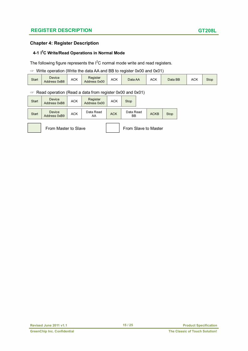
4-1 I2C Write/Read Operations in Normal Mode
The following figure represents the I2C normal mode write and read registers.
☞ Write operation (Write the data AA and BB to register 0x00 and 0x01)
Start Device Address 0xB8 ACK Register
Address 0x00 ACK Data AA ACK Data BB ACK Stop
☞ Read operation (Read a data from register 0x00 and 0x01)
Start Device Address 0xB8 ACK Register
Address 0x00 ACK Stop
Start Device Address 0xB9 ACK Data Read
AA ACK Data Read BB ACKB Stop
REGISTER DESCRIPTION
From Master to Slave From Slave to Master
The Classic of Touch Solution! GreenChip Inc. Confidential
Product Specification Revised June 2011 v1.1 16 / 25
GT208L
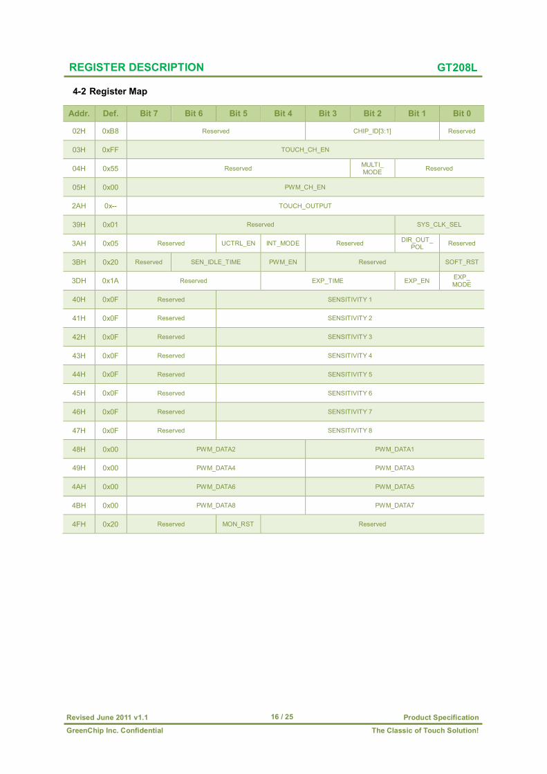
4-2 Register Map Addr. Def. Bit 7 Bit 6 Bit 5 Bit 4 Bit 3 Bit 2 Bit 1 Bit 0
02H 0xB8 Reserved CHIP_ID[3:1] Reserved
03H 0xFF TOUCH_CH_EN
04H 0x55 Reserved MULTI_ MODE Reserved
05H 0x00 PWM_CH_EN
2AH 0x-- TOUCH_OUTPUT
39H 0x01 Reserved SYS_CLK_SEL
3AH 0x05 Reserved UCTRL_EN INT_MODE Reserved DIR_OUT_ POL Reserved
3BH 0x20 Reserved SEN_IDLE_TIME PWM_EN Reserved SOFT_RST
3DH 0x1A Reserved EXP_TIME EXP_EN EXP_ MODE
40H 0x0F Reserved SENSITIVITY 1
41H 0x0F Reserved SENSITIVITY 2
42H 0x0F Reserved SENSITIVITY 3
43H 0x0F Reserved SENSITIVITY 4
44H 0x0F Reserved SENSITIVITY 5
45H 0x0F Reserved SENSITIVITY 6
46H 0x0F Reserved SENSITIVITY 7
47H 0x0F Reserved SENSITIVITY 8
48H 0x00 PWM_DATA2 PWM_DATA1
49H 0x00 PWM_DATA4 PWM_DATA3
4AH 0x00 PWM_DATA6 PWM_DATA5
4BH 0x00 PWM_DATA8 PWM_DATA7
4FH 0x20 Reserved MON_RST Reserved
REGISTER DESCRIPTION
The Classic of Touch Solution! GreenChip Inc. Confidential
Product Specification Revised June 2011 v1.1 17 / 25
GT208L
4-3 Register Description 4-3-1 Chip ID Control Registers - R/W ☞ Description: The GT208L chip ID. It can be set 0xB0 ~ 0xBF. This register control should be available when the CTRL pin is connected to open or VDD. Chip ID be set at 0xB4 when CTRL pin is connected to GND. (See 3-7 CTRL Pin Selection)
02H Bit7 Bit6 Bit5 Bit4 Bit3 Bit2 Bit1 Bit0 Name Reserved CHIP_ID[3:1] Reserved
Default 1 0 1 1 1 0 0 0
Addr. Bits Default Name Description
02H 7-4 1011B Reserved Fixed ‘1011’ = 0xBH
3-1 100B CHIP_ID[3:1] GT208L chip ID.
0 0B Reserved
4-3-2 Touch Channel Enable Registers - R/W ☞ Description: The GT208L supports eight each touch channel enable register.
03H Bit7 Bit6 Bit5 Bit4 Bit3 Bit2 Bit1 Bit0 Name TOUCH_CH_EN
Default 1 1 1 1 1 1 1 1
Addr. Bits Default Name Description 03H 7-0 FFH TOUCH_CH_EN 1~8 each touch channel enable
4-3-3 Single and Multi-touch Control Registers - R/W ☞ Description: The GT208L is supported single and multi touch mode. This register is available when UCTRL_EN(3AH[5]) is set or the CTRL pin is connected to VDD or Open.
04H Bit7 Bit6 Bit5 Bit4 Bit3 Bit2 Bit1 Bit0
Name Reserved MULTI_ MODE Reserved
Default 0 1 0 1 0 1 0 1
Addr. Bits Default Name Description
04H
7-3 01010B Reserved
2 1B MULTI_MODE GT208L single/multi touch mode 0 : single 1 : multi
1-0 01B Reserved
4-3-4 PWM Channel Enable Registers - R/W ☞ Description: The GT208L supports eight each PWM output generation.
05H Bit7 Bit6 Bit5 Bit4 Bit3 Bit2 Bit1 Bit0 Name PWM_CH_EN
Default 0 0 0 0 0 0 0 0
Addr. Bits Default Name Description
05H 7-0 00H PWM_CH_EN 1~8 each PWM channel enable 0: disable 1: enable
4-3-5 Touch Output Registers - R ☞ Description: An each touch channel status can be monitored.
2AH Bit7 Bit6 Bit5 Bit4 Bit3 Bit2 Bit1 Bit0 Name TOUCH_OUTPUT
Default - - - - - - - -
Addr. Bits Default Name Description 2AH 7-0 --H TOUCH_OUTPUT Touch channel detection monitoring
REGISTER DESCRIPTION
The Classic of Touch Solution! GreenChip Inc. Confidential
Product Specification Revised June 2011 v1.1 18 / 25
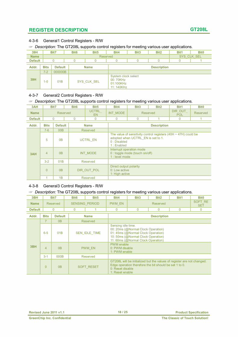
GT208L 4-3-6 General1 Control Registers - R/W ☞ Description: The GT208L supports control registers for meeting various user applications.
39H Bit7 Bit6 Bit5 Bit4 Bit3 Bit2 Bit1 Bit0 Name Reserved SYS_CLK_SEL
Default 0 0 0 0 0 0 0 1
Addr. Bits Default Name Description
39H
7-2 000000B
1-0 01B SYS_CLK_SEL
System clock select 00: 70KHz 01:100KHz 11: 140KHz
4-3-7 General2 Control Registers - R/W ☞ Description: The GT208L supports control registers for meeting various user applications.
3AH Bit7 Bit6 Bit5 Bit4 Bit3 Bit2 Bit1 Bit0
Name Reserved UCTRL_ EN INT_MODE Reserved DIR_OUT_
POL Reserved
Default 0 0 0 0 0 1 0 1
Addr. Bits Default Name Description
3AH
7-6 00B Reserved
5 0B UCTRL_EN
The value of sensitivity control registers (40H ~ 47H) could be adopted when UCTRL_EN is set to 1. 0 : Disabled 1 : Enabled
4 0B INT_MODE Interrupt operation mode 0 : toggle mode (touch on/off) 1 : level mode
3-2 01B Reserved
0 0B DIR_OUT_POL Direct output polarity 0: Low active 1: High active
1 1B Reserved 4-3-8 General3 Control Registers - R/W ☞ Description: The GT208L supports control registers for meeting various user applications.
3BH Bit7 Bit6 Bit5 Bit4 Bit3 Bit2 Bit1 Bit0
Name Reserved SENSING_PERIOD PWM_EN Reserved SOFT_RESET
Default 0 0 1 0 0 0 0 0
Addr. Bits Default Name Description
3BH
7 0B Reserved
6-5 01B SEN_IDLE_TIME
Sensing idle time. 00: 20ms (@Normal Clock Operation) 01: 45ms (@Normal Clock Operation) 10: 50ms (@Normal Clock Operation) 11: 60ms (@Normal Clock Operation)
4 0B PWM_EN PWM enable 0: PWM disable 1: PWM enable
3-1 000B Reserved
0 0B SOFT_RESET
GT208L will be initialized but the values of register are not changed. Edge operation therefore the bit should be set 1 to 0. 0: Reset disable 1: Reset enable
REGISTER DESCRIPTION
The Classic of Touch Solution! GreenChip Inc. Confidential
Product Specification Revised June 2011 v1.1 19 / 25
GT208L 4-3-9 Expiration Control Registers - R/W ☞ Description: The GT208L supports control registers for meeting various user applications.
3DH Bit7 Bit6 Bit5 Bit4 Bit3 Bit2 Bit1 Bit0
Name Reserved EXP_TIME EXP_ EN EXP_ MODE
Default 0 0 0 1 1 0 1 0
Addr. Bits Default Name Description
3DH
7-5 000B Reserved
4-2 110B EXP_TIME Time = (EXP_TIME) x 16 period (approximate)
1 1B EXP_ EN Touch expire enable 0: Disable 1: Enable
0 0B EXP_ MODE Touch expire mode 0 : Expire count is not restarted in a touch state 1 : Expire count is restarted if a different touch occur
4-3-10 Sensitivity Control Registers - R/W ☞ Description: The GT208L can be controlled independently for getting the optimal sensitivity on each channel.
XXH Bit7 Bit6 Bit5 Bit4 Bit3 Bit2 Bit1 Bit0 Name Reserved SENSITIVITY n
Default 0 0 0 0 1 1 1 1
Addr. Bits Default Name Description
40H
7-6 00B Reserved
5-0 0FH SENSITIVITY 1
Channel 1 touch sensitivity UCTRL_EN(3AH[5]) must be set ‘1’. Otherwise, Sensitivity follows CTRL pin connection. 0x02 : Highest Sensitivity 0x3F : Lowest Sensitivity
41H
7-6 00B Reserved
5-0 0FH SENSITIVITY 2
Channel 2 touch sensitivity UCTRL_EN(3AH[5]) must be set ‘1’. Otherwise, Sensitivity follows CTRL pin connection. 0x02 : Highest Sensitivity 0x3F : Lowest Sensitivity
42H
7-6 00B Reserved
5-0 0FH SENSITIVITY 3
Channel 3 touch sensitivity UCTRL_EN(3AH[5]) must be set ‘1’. Otherwise, Sensitivity follows CTRL pin connection. 0x02 : Highest Sensitivity 0x3F : Lowest Sensitivity
43H
7-6 00B Reserved
5-0 0FH SENSITIVITY 4
Channel 4 touch sensitivity UCTRL_EN(3AH[5]) must be set ‘1’. Otherwise, Sensitivity follows CTRL pin connection. 0x02 : Highest Sensitivity 0x3F : Lowest Sensitivity
44H
7-6 00B Reserved
5-0 0FH SENSITIVITY 5
Channel 5 touch sensitivity UCTRL_EN(3AH[5]) must be set ‘1’. Otherwise, Sensitivity follows CTRL pin connection. 0x02 : Highest Sensitivity 0x3F : Lowest Sensitivity
45H
7-6 00B Reserved
5-0 0FH SENSITIVITY 6
Channel 6 touch sensitivity UCTRL_EN(3AH[5]) must be set ‘1’. Otherwise, Sensitivity follows CTRL pin connection. 0x02 : Highest Sensitivity 0x3F : Lowest Sensitivity
46H 7-6 00B Reserved
5-0 0FH SENSITIVITY 7 Channel 7 touch sensitivity UCTRL_EN(3AH[5]) must be set ‘1’. Otherwise, Sensitivity follows
REGISTER DESCRIPTION
The Classic of Touch Solution! GreenChip Inc. Confidential
Product Specification Revised June 2011 v1.1 20 / 25
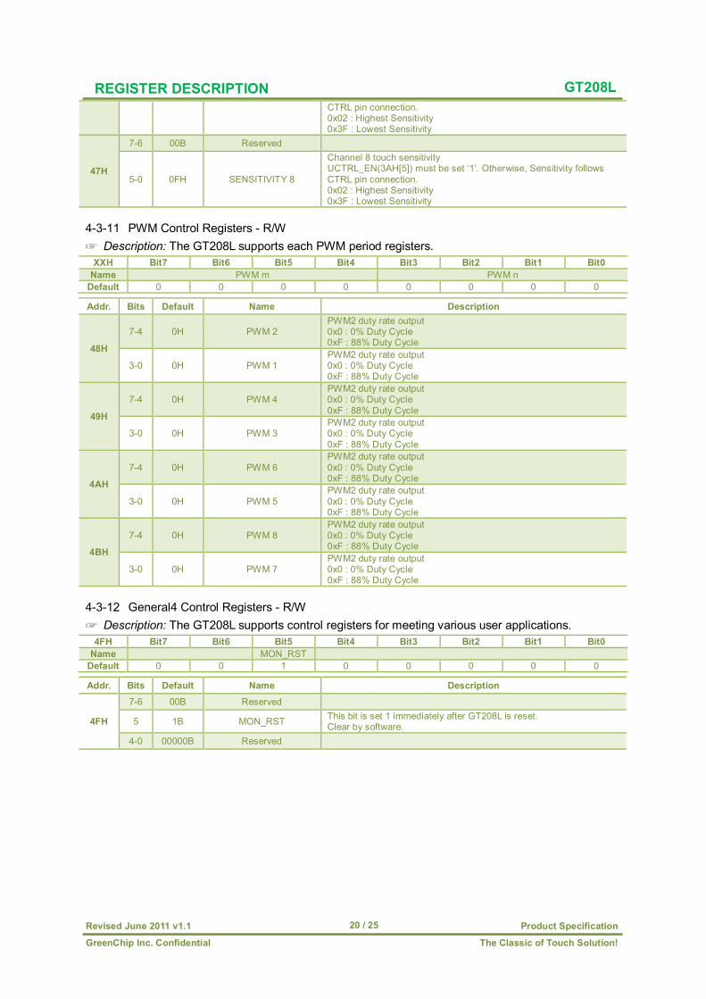
GT208L CTRL pin connection. 0x02 : Highest Sensitivity 0x3F : Lowest Sensitivity
47H
7-6 00B Reserved
5-0 0FH SENSITIVITY 8
Channel 8 touch sensitivity UCTRL_EN(3AH[5]) must be set ‘1’. Otherwise, Sensitivity follows CTRL pin connection. 0x02 : Highest Sensitivity 0x3F : Lowest Sensitivity
4-3-11 PWM Control Registers - R/W ☞ Description: The GT208L supports each PWM period registers.
XXH Bit7 Bit6 Bit5 Bit4 Bit3 Bit2 Bit1 Bit0 Name PWM m PWM n
Default 0 0 0 0 0 0 0 0
Addr. Bits Default Name Description
48H
7-4 0H PWM 2 PWM2 duty rate output 0x0 : 0% Duty Cycle 0xF : 88% Duty Cycle
3-0 0H PWM 1 PWM2 duty rate output 0x0 : 0% Duty Cycle 0xF : 88% Duty Cycle
49H
7-4 0H PWM 4 PWM2 duty rate output 0x0 : 0% Duty Cycle 0xF : 88% Duty Cycle
3-0 0H PWM 3 PWM2 duty rate output 0x0 : 0% Duty Cycle 0xF : 88% Duty Cycle
4AH
7-4 0H PWM 6 PWM2 duty rate output 0x0 : 0% Duty Cycle 0xF : 88% Duty Cycle
3-0 0H PWM 5 PWM2 duty rate output 0x0 : 0% Duty Cycle 0xF : 88% Duty Cycle
4BH
7-4 0H PWM 8 PWM2 duty rate output 0x0 : 0% Duty Cycle 0xF : 88% Duty Cycle
3-0 0H PWM 7 PWM2 duty rate output 0x0 : 0% Duty Cycle 0xF : 88% Duty Cycle
4-3-12 General4 Control Registers - R/W ☞ Description: The GT208L supports control registers for meeting various user applications.
4FH Bit7 Bit6 Bit5 Bit4 Bit3 Bit2 Bit1 Bit0 Name MON_RST
Default 0 0 1 0 0 0 0 0
Addr. Bits Default Name Description
4FH
7-6 00B Reserved
5 1B MON_RST This bit is set 1 immediately after GT208L is reset. Clear by software.
4-0 00000B Reserved
REGISTER DESCRIPTION
The Classic of Touch Solution! GreenChip Inc. Confidential
Product Specification Revised June 2011 v1.1 21 / 25
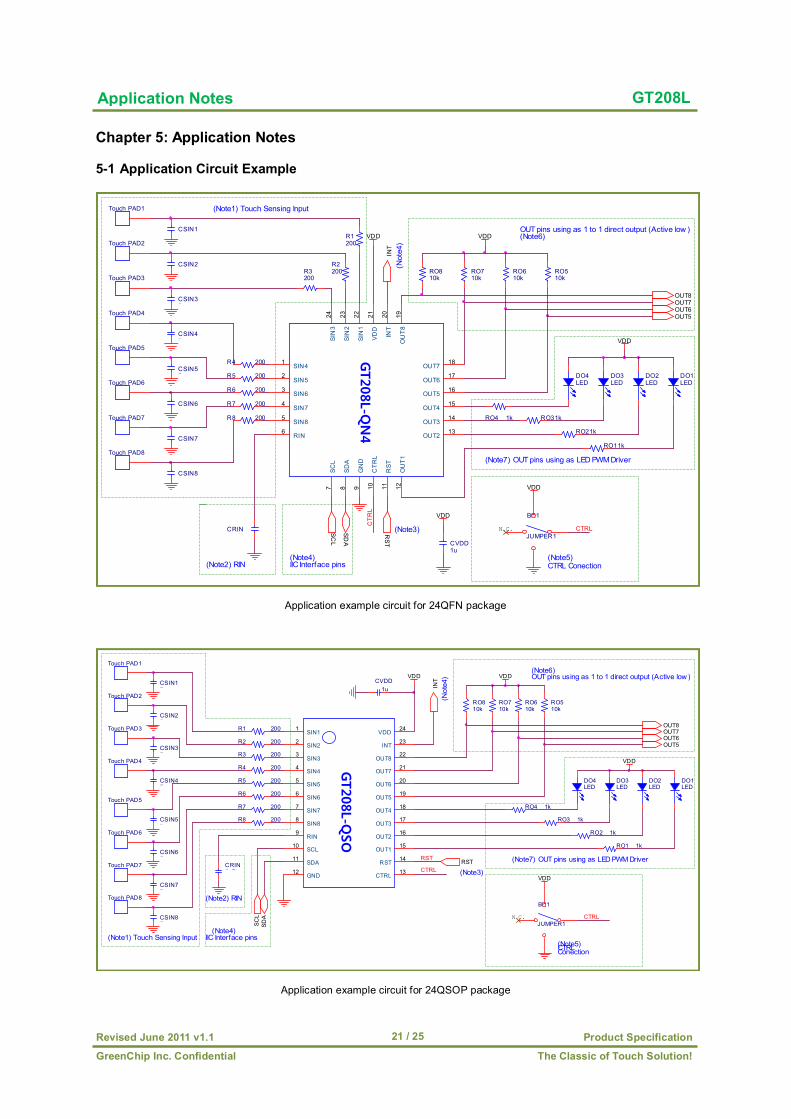
GT208L Chapter 5: Application Notes 5-1 Application Circuit Example
Application example circuit for 24QFN package
Application example circuit for 24QSOP package
BR1
JUMPER1
CSIN45p
DO3LED
VDD
CSIN35p
RO11k
OUT7
R7 200
R4 200
GT108L-Q
N4
4
3
2
5
6
7 10 128 9 11
13
14
15
16
17
18
192021222324
1
SIN7
SIN6
SIN5
SIN8
RIN
SCL
CTR
L
OU
T1
SDA
GN
D
RST
OUT2
OUT3
OUT4
OUT5
OUT6
OUT7
OU
T8INT
VDD
SIN
1
SIN
2
SIN
3
SIN4
Touch PAD5
R8 200
R5 200
RO810k
CTRL
OUT pins using as LED PWM Driver
Touch PAD3RO510k
(Note4)
RO710k
DO2LED
CSIN55p
CSIN65p
(Note2) RIN
Touch PAD7
VDD
Touch PAD4
DO1LED
(Note6)
Touch PAD1
OUT6
CSIN25p
OUT pins using as 1 to 1 direct output (Active low )
IIC Interface pins
VDD
RO4 1k
R3200
CVDD1u
(Note7)
RO21k
OUT5
R1200
RO31k
RST
SCL
(Note3)
RO610k
SDA
(Not
e4)
Touch PAD6
N.C.
CSIN85p
(Note1) Touch Sensing Input
DO4LED
R6 200
OUT8
VDD
(Note5) CTRL Conection
Touch PAD8
CSIN75p
Touch PAD2
R2200
VDD
INT
CRIN5p+3~4pF
CSIN15p
CTR
L
R5 200
(Note4)
RO610k
CSIN35p
OUT8
R4 200
OUT7
Touch PAD4
R2 200
RO510k
CTRL
VDD
RO710k
Touch PAD6
CSIN65p
Touch PAD5
OUT pins using as 1 to 1 direct output (Active low )
OUT5
RO3 1k
(Note3)
R8 200
DO1LED
(Note7)RST
(Note2) RIN
Touch PAD7
(Note6)
SDA
R7 200
CSIN85p
(Not
e4)
IIC Interface pins
VDD
RST
INT
Touch PAD3
CSIN45p
Touch PAD8
(Note1) Touch Sensing Input
GT108L-Q
SO
7
6
5
8
11
13
10
12
15
16
17
18
19
23
241
2
3
4
22
9
14
20
21
SIN7
SIN6
SIN5
SIN8
SDA
CTRL
SCL
GND
OUT1
OUT2
OUT3
OUT4
OUT5
INT
VDDSIN1
SIN2
SIN3
SIN4
OUT8
RIN
RST
OUT6
OUT7
R1 200
RO1 1k
CSIN25p
OUT6
RO810k
CSIN15p
R6 200
N.C.
RO2 1k
SCL
RO4 1k
(Note5) CTRLConection
DO4LED
DO2LED
VDD
Touch PAD1
DO3LED
Touch PAD2
VDD
CVDD1u
CTRL
OUT pins using as LED PWM Driver
CSIN75p
CRIN5pF
R3 200
CSIN55p
BR1
JUMPER1
Application Notes
GT208L-Q
SO
GT208L-Q
N4
The Classic of Touch Solution! GreenChip Inc. Confidential
Product Specification Revised June 2011 v1.1 22 / 25
GT208L 5-2 Application Notes Normally a touch sensing operation is ultimately impedance variation sensing. Hence a touch sensing system is recommended to be taken care of prevention of the external sensing disturbance. Although the GT208L has enough noise rejection algorithms and various protection circuits to prevent error touch detection caused by noise and incapable sensing, it is better to take care in noisy applications such as home appliances. There are many measurable or invisible noises in system that can affect the impedance sensing signal or distort that signal. The main principal design issues and required attentions are such as below. 5-2-1 Power Line The touch sensor power line is recommended to be split from the other power lines such as relay
circuits or LED that can make pulsation noise on their power lines. The big inductance that might exist in long power connection line can cause power fluctuation by
other noise sources. The lower frequency periodic power noise such as a few Hz ~ kHz has more baneful influence on
sensitivity calibration. An extra regulator for touch sensor is desirable for prevention above power line noises. The VDD under shooting pulse less than internal reset voltage (VDD_RST) can cause system reset. The capacitor connected between VDD and GND is somehow obligation element for buffering
above power line noises. This capacitor must be placed as near to IC as possible.
5-2-2 Sensing (Reference) Input Line for Touch Detect <Note1><Note2> The sensing lines for touch detection are desirable to be routed as short as possible and the
width of routing path should be as narrow as possible. The sensing line for touch detection should be formed by bottom metal, in other words, an
opposite metal of a touch PAD. The additional extension line pattern of RIN input on application PCB can help prevention of
abnormal actions caused by radiation noise, but excessive long RIN input line can be a reason for failure of touch detect.
SIN capacitor is useful for sensitivity reduction adjust. A bigger capacitor of SIN makes sensitivity of corresponding channel to be lower.
RIN capacitor value is about average value of SIN inputs capacitors. The sensing line for touch detection is desirable to be routed as far as possible from impedance
varying path such as LED drive current path. An unused sensing channel is desirable to be turned off by control register. (Recommendation) Additional external series resistors are profitable for prevention of abnormal actions caused by
radiation noise or electrical surge pulse. The series resistor value should be less than 1kΩ and the location of resister is better as near as possible to the SIN ports for better stable operation. (Refer to 3-2)
All touch sensing pads are recommended to be surrounded by GND pattern to reduce noise influence.
5-2-4 External Reset <Note3> The RST port is for the abrupt reset input signal. The high pulse signal can make system reset.
This port has also an internal pull-down resistor hence the RST port can be floating. (Refer to 3-1) 5-2-5 I2C Interface Applications <Note4> The SCL is I2C clock input port and SDA is I2C data input/output port. SCL and SDA have internal
optional pull-up resistor. So, when I2C interface is not required, SCL and SDA ports can be floating. For high speed communication, SDA port needs small pull-up resistor connected to VDD to reduce pulse rising delay. (Refer to 3-5)
INT is for the output signal that indicates changing of sensing output data. This port is output only port and has active low function. Because INT pin has open drain structure, pull-up resistor is required for valid output.(Refer to 3-6)
Application Notes
The Classic of Touch Solution! GreenChip Inc. Confidential
Product Specification Revised June 2011 v1.1 23 / 25
GT208L 5-2-6 Sensitivity Selection <Note5> Three optional sensitivities are available by CTRL pin connection. Open connection (e.g. N.C.)
comes to normal sensitivity, VDD connection comes to low sensitivity, and GND connection comes to high sensitivity. This sensitivity selection is valid for all sensing channels. (Refer to 3-7)
5-2-7 1 to 1 Direct Output Applications <Note6> The ports that are used for 1 to 1 direct output have an active low and high output mode. Both
output modes are all open drain type. Therefore a pull-up or a pull-down resistor is required for a valid output. The OUTx port corresponds to SINx sense input respectively. (Refer to 3-4)
5-2-8 LED PWM Drive applications <Note7> The maximum 10mA LED drive current can be sunk by a single OUT port on typical temperature
condition. The OUT ports which are used as LED PWM drive ports cannot carry out the role of 1 to 1 direct out simultaneously. The 16 steps brightness control is possible. (Refer to 3-3)
Application Notes
The Classic of Touch Solution! GreenChip Inc. Confidential
Product Specification Revised June 2011 v1.1 24 / 25
GT208L Chapter 6: Package information
6-1 Package Outside Drawings for GT208L-QN4
Note : All dimensions are in mm. Angles in degree.
PACKAGE INFORMATION
The Classic of Touch Solution! GreenChip Inc. Confidential
Product Specification Revised June 2011 v1.1 25 / 25
GT208L 6-2 Package Outside Drawings for GT208L-QSO
Note : All dimensions are in mm. Angles in degree.
PACKAGE INFORMATION
![Touch Technologies Tutorial · Emerging Touch Technologies With Multi-Touch [58] Projected Capacitive LCD In-Cell (Optical, Switch & Capacitive) Optical Digital Resistive Waveguide](https://img.pdfslide.net/doc/110x75/6000f3e8fa24967a0f056959/touch-technologies-tutorial-emerging-touch-technologies-with-multi-touch-58-projected.jpg)