Embed Size (px)
Citation preview
Grinding of Single-Crystal Silicon AlongCrystallographic Directions
Z. W. Zhong* and W. H. Tok
School of Mechanical & Production Engineering,Nanyang Technological University, Singapore
ABSTRACT
This article studies the effect of grinding along crystallographic directions on thesurface finish of single-crystal silicon. It also discusses new and=or improved pro-cesses for precision machining brittle materials, including silicon. Silicon sampleswere cut from (100) silicon wafers. These samples were then subjected to grindingalong different crystallographic directions under the same experimental condi-tions. The surface roughness and the surface texture of these samples were thenanalyzed. The Ra and Rq values and the microphotographs of the ground siliconsurfaces showed the dependency of surface finish on the grinding direction. Bettersurface finish was achieved when (100) silicon was ground along h110i directions.Samples ground along these directions also showed more ductile streaks on thesilicon surfaces, compared with surfaces ground along the other directions.
Key Words: Grinding; Single crystal; Silicon; Crystallographic direction; Brittlematerial; Surface roughness; Wafer; Experiment; Surface texture; Slip direction;Ductile streak; Pitting damage; Crystal structure; Miller indices; Microphoto-graph.
*Correspondence: Z. W. Zhong, School of Mechanical & Production Engineering, NanyangTechnological University, 50 Nanyang Ave., Singapore 639798; E-mail: [email protected].
MATERIALS AND MANUFACTURING PROCESSES
Vol. 18, No. 5, pp. 811–824, 2003
811
DOI: 10.1081/AMP-120024977 1042-6914 (Print); 1532-2475 (Online)
Copyright # 2003 by Marcel Dekker, Inc. www.dekker.com
1.0. INTRODUCTION
Silicon is one of the most abundant materials on the earth’s surface, representingapproximately 25% of the earth’s crust. Silicon is mainly used as an integrated circuit(IC) carrier in microelectronics. The silicon used in the fabrication of semiconductordevices is extremely pure. Before device manufacture is started, the silicon has atypical impurity concentration of less than one part per billion. ICs and discretesolid-state devices are manufactured on wafers made of single-crystal silicon.Single-crystal silicon is also the most widely used substrate material for microelectro-mechancial systems (MEMS) and microsystems. It is the prime candidate materialfor sensors and actuators, and is the common substrate for microfluidics.[1–3]
Semiconductors are commonly inorganic materials made from elements in thefourth column (group IV) of the periodic table. These materials are neither goodconductors nor good insulators, hence the name, semiconductors. The two most com-mon materials used in the production of semiconductor devices are crystalline ger-manium and silicon, although silicon dominates the market. Both these materialspossess qualities that offer advantages for specific applications. Silicon can be mod-ified in several ways to change its electrical, mechanical, and optical properties. Theuse of silicon in solid state and microelectronics has shown a spectacular growthsince the early 1970s, and this growth pattern is still continuing.[4,5]
Silicon is also used for optical components in high-resolution thermal imagingsystems. Si and Ge are the most widely used thermal imaging materials operatingin the middle infrared to far infrared wavelength regions. Parabolic surfaces on Siprove to be a good choice for infrared applications.[6]
Two wafers with surfaces that are sufficiently smooth, flat, and clean can bond toeach other without any adhesive or external forces at room temperature in ambientair. This technology is called wafer bonding and has been gaining interest for a num-ber of microprocessing applications: high-performance microelectronics, photonics,optoelectronics, and MEMS. Modern wafer bonding is driven by the demand toenhance the IC performance.[7]
Apart from the increase in quantity of manufacturing of pure silicon, qualityrequirements have also increased. A steady increase in chip surface area producedannually is expected, and this will be accompanied by an increasing degree ofcomponent integration.[8]
In this article, past research work with new and=or improved processes for pre-cision machining brittle materials, including silicon, is reviewed. Then the fundamen-tal theories essential to this study are discussed. Finally, experiments carried out tostudy the effect of grinding along crystallographic directions on the surface finish ofsingle-crystal silicon are reported with promising results.
2.0. LITERATURE REVIEW
Typical processes in the manufacturing of silicon-based devices are as follows. Aseed crystal of silicon is placed on the end of a rod and dipped into a vat of moltensilicon. The rod is slowly withdrawn from the vat, and during this withdrawalprocess, the silicon in contact with the seed crystal slowly cools and the crystal of
812 Zhong and Tok

silicon grows. The end result is an ingot of silicon that is usually not less than 50 cmlong. This ingot is then sawed into slices called wafers, and both surfaces of thewafers are ground, lapped, and polished to form a smooth finish. The last step ofwafer preparation is a chemical etching of one side to remove any final irregularitiesand possible damage that are left from the polishing process. The next step is toadd the desired characteristics=devices to the material, then cut the wafer into manysmall pieces called dice or chips, and finally, assemble the chips into a protectivepackage.[4]
There has been research in dealing with the traditional surface finishing pro-cesses such as cutting, grinding, and polishing of wafers, as well as more untradi-tional methods.[9] However, the industrial implementation of these new processesis still not possible due to reasons such as low throughput, high equipment cost,and so on.
Mechanical grinding gives high dimensional accuracy and good total thicknessvariation (TTV). Because it induces mechanical damage on surfaces, surface etchingor polishing is necessary to remove the damaged area. During these etching andpolishing processes, TTV is usually degraded. To improve TTV, etching and polish-ing should be reduced. In other words, reduction of surface damage depth duringgrinding is necessary.[7]
Precision machining of brittle material such as silicon and ceramics is based on ahypothesis, which states that all materials regardless of their hardness and brittlenesswill undergo a transition from a brittle to a ductile machining region below a criticaldepth of cut. Below this threshold, the energy required to propagate cracks isbelieved to be larger than that required for plastic deformation. Hence, plastic defor-mation is the predominant mechanism of material removal for ductile mode machin-ing of brittle materials. Therefore, by cutting or grinding at an extremely small depthof cut, a brittle material is able to deform in a ductile manner, thus giving bettersurface finish.[10]
A cutting technique using a flying tool under negative pressure was proposed forcutting brittle materials without cracking.[11] A flying tool glided over a workpiecesurface while maintaining a small height like a negative pressure slider of a magneticdisk drive. Using this tool system, ductile regime cutting of optical glass and single-crystal silicon was examined, and a mirror surface finish with no cracks was achievedon a lathe having a 0.1-mm order of error motion.
Diamond turning of single-crystal silicon was carried out along all the crystallo-graphic directions on the (001) and (111) planes at depths of cut of 0.1 and 1 mm, andthe mechanism involved in ductile regime turning was studied.[12] Pitting damage wasobserved along some crystallographic orientations. The crystallographic orientationdependence of the surface features was also observed to change with the depth of cut.By using transmission electron microscopy on the f111gh110i slip systems, it wasfound that the orientation dependence of the surface features was closely linked tothe ease with which slip deformation occurred.
Ultrasonic vibration was introduced into the grooving process of brittle materi-als by a vibration exciter exciting the cutting tool.[13] Roughness of the side surfacewas improved by low-frequency vibration, ultrasonic vibration, and combined vibra-tion. When the amplitude of low-frequency vibration was increased, the surfaceroughness was further improved.
Grinding of Single-Crystal Silicon 813

The material removal mechanism in grinding of ceramics using diamond wheelswas also studied.[10] Material pulverization was discovered on the surface layer ofground ceramics. The pulverized material was loosely connected in comparison tothe bulk material, and could be recompacted by hydrostatic compressive stress inthe contact region at the interface of the abrasive grain and the workpiece. Materialflowed sideways in single-point grinding, forming pile-ups on both sides of a groove.
Grinding of toroidal and cylindrical surfaces made of Si and SiC was carried outby using diamond grinding wheels and an inexpensive computerized, numericallycontrolled (CNC) machining center.[14,15] Mirrors were successfully obtained byautomatic grinding operations with good shape accuracy, mirror surface finish,and low roughness heights. Ductile-mode material removal was achieved by grindingwith dressing. Scanning electron microscopy (SEM) microphotographs demon-strated the ductile mode in grinding of silicon. Ground silicon carbide had almostcomplete ductile mode surfaces, and the surface roughness was independent of thedirection of measurement.
Nanogrinding was performed based on a lapping process.[16] The abrasive grainswere completely embedded in a soft metallic plate that was the grinding tool. Pumicewas embedded in the grinding plate and remained there throughout the process.Between pumice particles, the basic soft metallic-plate materials formed the plateaus.Diamond grains were then embedded by a conditioning ring with their summitsaligned coplanar to the plate surface. This arrangement resulted in plastic materialremoval, minimal subsurface damage, and excellent surface finish.
A special grinding wheel was developed for machining silicon wafers.[17] Thewheel acted like a grinding wheel when sufficient fluid was provided. It producedsimilar roughness and removal rate to a conventional lapping tool when the flow ratewas below a certain value. Surfaces obtained by using this grinding wheel had bettersurface roughness than that obtained by conventional processes.
Electrophoretic deposition is a phenomenon whereby an electric field is appliedto a solution of ionic particles. The particles will adhere to the anode. Making useof this theory, ultrafine abrasives can be deposited to the grinding wheel. It wasreported that a mirror surface without chipping was achieved by using this method.[18]
By using a new device for dressing a resin-bonded diamond wheel and animproved coolant system, ductile-mode grinding of silicon and glass was achievedusing an inexpensive, conventional surface grinding machine.[19] The low-cost dres-sing device also ensured minimum disruption to the grinding operation and a higherlevel of safety. A flooding supply of coolant at the grinding zone provided bettercooling performance and lubrication.
An in-process dressing study was performed using a water jet.[20] It was foundthat the water jet removed the chips embedded in the space between the protrusionof the abrasive grains on the wheel. If the water pressure was too low, the in-processdressing was not effective. If the pressure was too high, the wheel became eroded.
Electrodischarge machine (EDM) dressing can be used for in-process dressingof the grinding wheel to obtain high truing efficiency.[21] The truing accuracy ofEDM dressing not only depends on the electric parameters, but also on the precisionof the equipment and balance of the wheel. For the grains of the grinding wheel notto be covered, removed, or emerged, the removal volume of a single EDM pulsemust be less than the size of the diamond grain.
814 Zhong and Tok
3.0. SLIP DIRECTION AND SILICON LATTICE STRUCTURE
When dealing with crystalline materials, it often becomes necessary to specifysome particular crystallographic plane of atoms or crystallographic directions. Themost common way of doing this is using the Miller indices.[22,23]
Dislocations do not move with the same degree of ease on all crystallographicplanes of atoms and in all crystallographic directions. There are preferred slip planesand specific slip directions along which dislocation motion tends to occur. In otherwords, plastic deformation occurs primarily by sliding over certain planes. Slipoccurs predominantly on crystallographic planes of maximum atomic density. Inaddition, slip will occur in the closed-packed direction, which represents the shortestdistance between two equilibrium atom positions and the lowest energy direction.Slip systems (combinations of slip planes and directions) are such that the atomicdistortion that accompanies the motion of a dislocation is a minimum. The domi-nant slip systems vary with crystal structures of materials, because the relativeatomic densities of planes and directions are different.[22,24]
Silicon is one of a very few materials that can be economically manufactured as asingle-crystal substrate. It, like other group IV insulators and semiconductors includ-ing diamond, germanium, and gray tin, crystallizes in the diamond lattice structurethat can be regarded as simple cube. In other words, the primitive unit, the smallestrepeating block, of the crystal lattice resembles a cube.[3,25,26] It has an uneven latticegeometry for its atoms, but has basically a face-centered cubic (FCC) unit cell.[2]
Indeed, the crystal structure of silicon is more complex than that of a regularFCC structure. The diamond structure consists of two interpenetrating FCC sub-cubes with the origin of one displaced 1
41414 from the other. That is, one atom of
the second subcube occupies the site at one-fourth of the distance along a majordiagonal of the first subcube.[26] Because of the asymmetrical and nonuniform latticedistance between atoms, single-crystal silicon exhibits anisotropic thermophysicaland mechanical characteristics.[2]
The idea for the experiments reported in this article is that it should be possibleto achieve better surface finish when grinding along certain specific directions wheredislocation motions will most likely occur.
4.0. EXPERIMENTS
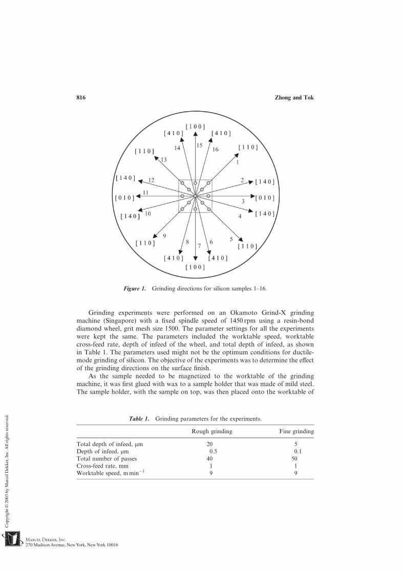
Silicon samples were cut from (100) wafers by using a method known asdiamond scribing. The surface of the wafer was marked or scribed with a diamondcutter. Then, by bending the wafer along the scribed lines, the wafer would breakalong the lines.[1] However, the wafer would only break in specific directions. Thesepreferred directions for breaking were perpendicular to each other.
As the wafer only broke in specific directions, it was not possible to cut out sam-ples according to the crystallographic orientations that were of interest to theauthors. Instead, 16 samples were cut with the same orientation and then placed withvarious orientations when they were subjected to grinding. The placement of the 16silicon samples was according to the crystallographic directions as shown in Fig. 1.
Grinding of Single-Crystal Silicon 815
Grinding experiments were performed on an Okamoto Grind-X grindingmachine (Singapore) with a fixed spindle speed of 1450 rpm using a resin-bonddiamond wheel, grit mesh size 1500. The parameter settings for all the experimentswere kept the same. The parameters included the worktable speed, worktablecross-feed rate, depth of infeed of the wheel, and total depth of infeed, as shownin Table 1. The parameters used might not be the optimum conditions for ductile-mode grinding of silicon. The objective of the experiments was to determine the effectof the grinding directions on the surface finish.
As the sample needed to be magnetized to the worktable of the grindingmachine, it was first glued with wax to a sample holder that was made of mild steel.The sample holder, with the sample on top, was then placed onto the worktable of
Figure 1. Grinding directions for silicon samples 1–16.
Table 1. Grinding parameters for the experiments.
Rough grinding Fine grinding
Total depth of infeed, mm 20 5Depth of infeed, mm 0.5 0.1Total number of passes 40 50Cross-feed rate, mm 1 1Worktable speed, mmin�1 9 9
816 Zhong and Tok
the grinding machine such that the investigated crystallographic orientation of thesample was parallel to the grinding direction. The worktable was then magnetizedto hold the sample holder in place. Because deep infeed could cause surface or sub-surface damage to the silicon sample, the infeed depth of rough grinding was set at0.5 mm. A dressing device developed[19] was used to dress the diamond wheel. Thiswas to ensure that the condition of the grinding wheel was the same for fine grindingall the samples. The dressing sticks used were composed of WA400G aluminumoxide.
5.0. RESULTS AND DISCUSSION
The surfaces of the ground samples were measured perpendicular to the grindingdirection for their roughness values using a Taylor-Hobson stylus profilometer. Thenmicroscope pictures were taken to examine the surfaces.
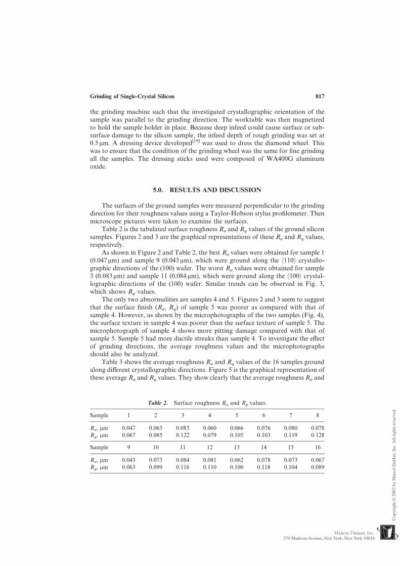
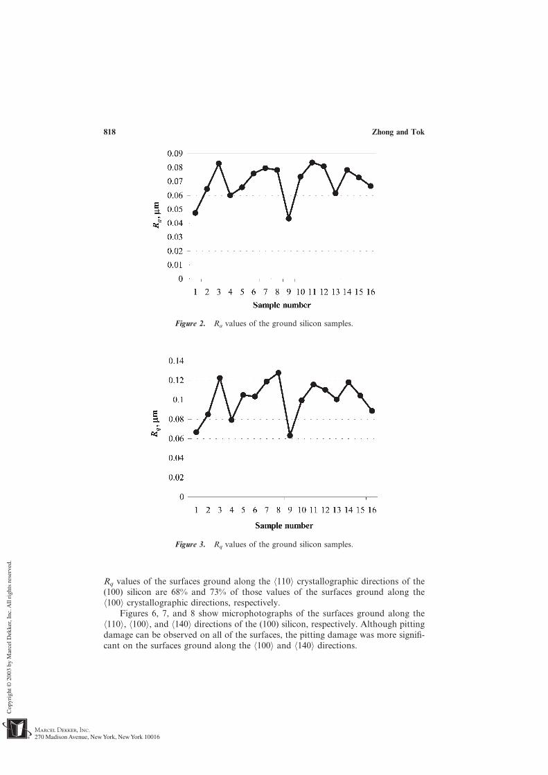
Table 2 is the tabulated surface roughness Ra and Rq values of the ground siliconsamples. Figures 2 and 3 are the graphical representations of these Ra and Rq values,respectively.
As shown in Figure 2 and Table 2, the best Ra values were obtained for sample 1(0.047 mm) and sample 9 (0.043 mm), which were ground along the h110i crystallo-graphic directions of the (100) wafer. The worst Ra values were obtained for sample3 (0.083 mm) and sample 11 (0.084 mm), which were ground along the h100i crystal-lographic directions of the (100) wafer. Similar trends can be observed in Fig. 3,which shows Rq values.
The only two abnormalities are samples 4 and 5. Figures 2 and 3 seem to suggestthat the surface finish (Ra, Rq) of sample 5 was poorer as compared with that ofsample 4. However, as shown by the microphotographs of the two samples (Fig. 4),the surface texture in sample 4 was poorer than the surface texture of sample 5. Themicrophotograph of sample 4 shows more pitting damage compared with that ofsample 5. Sample 5 had more ductile streaks than sample 4. To investigate the effectof grinding directions, the average roughness values and the microphotographsshould also be analyzed.
Table 3 shows the average roughness Ra and Rq values of the 16 samples groundalong different crystallographic directions. Figure 5 is the graphical representation ofthese average Ra and Rq values. They show clearly that the average roughness Ra and
Table 2. Surface roughness Ra and Rq values.
Sample 1 2 3 4 5 6 7 8
Ra, mm 0.047 0.065 0.083 0.060 0.066 0.076 0.080 0.078Rq, mm 0.067 0.085 0.122 0.079 0.105 0.103 0.119 0.128
Sample 9 10 11 12 13 14 15 16
Ra, mm 0.043 0.073 0.084 0.081 0.062 0.078 0.073 0.067Rq, mm 0.063 0.099 0.116 0.110 0.100 0.118 0.104 0.089
Grinding of Single-Crystal Silicon 817
Rq values of the surfaces ground along the h110i crystallographic directions of the(100) silicon are 68% and 73% of those values of the surfaces ground along theh100i crystallographic directions, respectively.
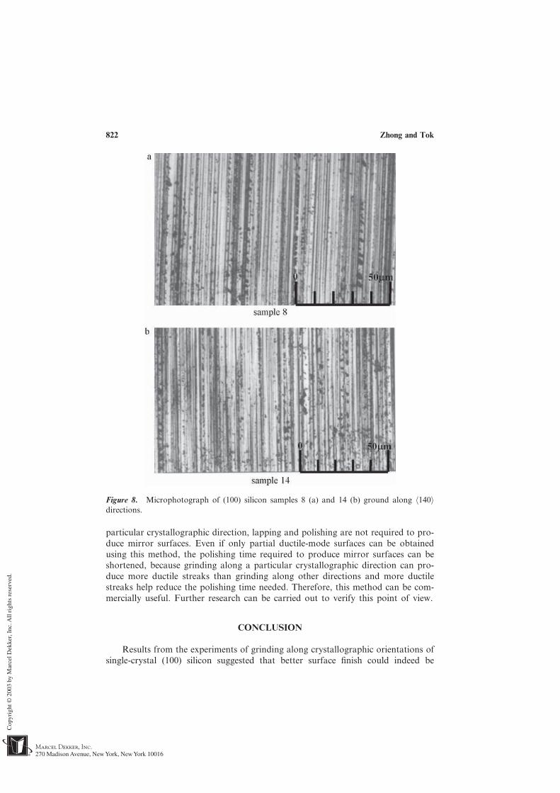
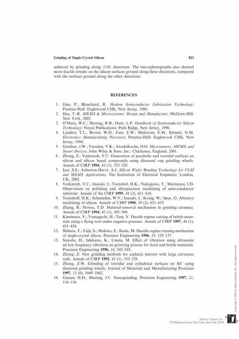
Figures 6, 7, and 8 show microphotographs of the surfaces ground along theh110i, h100i, and h140i directions of the (100) silicon, respectively. Although pittingdamage can be observed on all of the surfaces, the pitting damage was more signifi-cant on the surfaces ground along the h100i and h140i directions.
Figure 3. Rq values of the ground silicon samples.
Figure 2. Ra values of the ground silicon samples.
818 Zhong and Tok
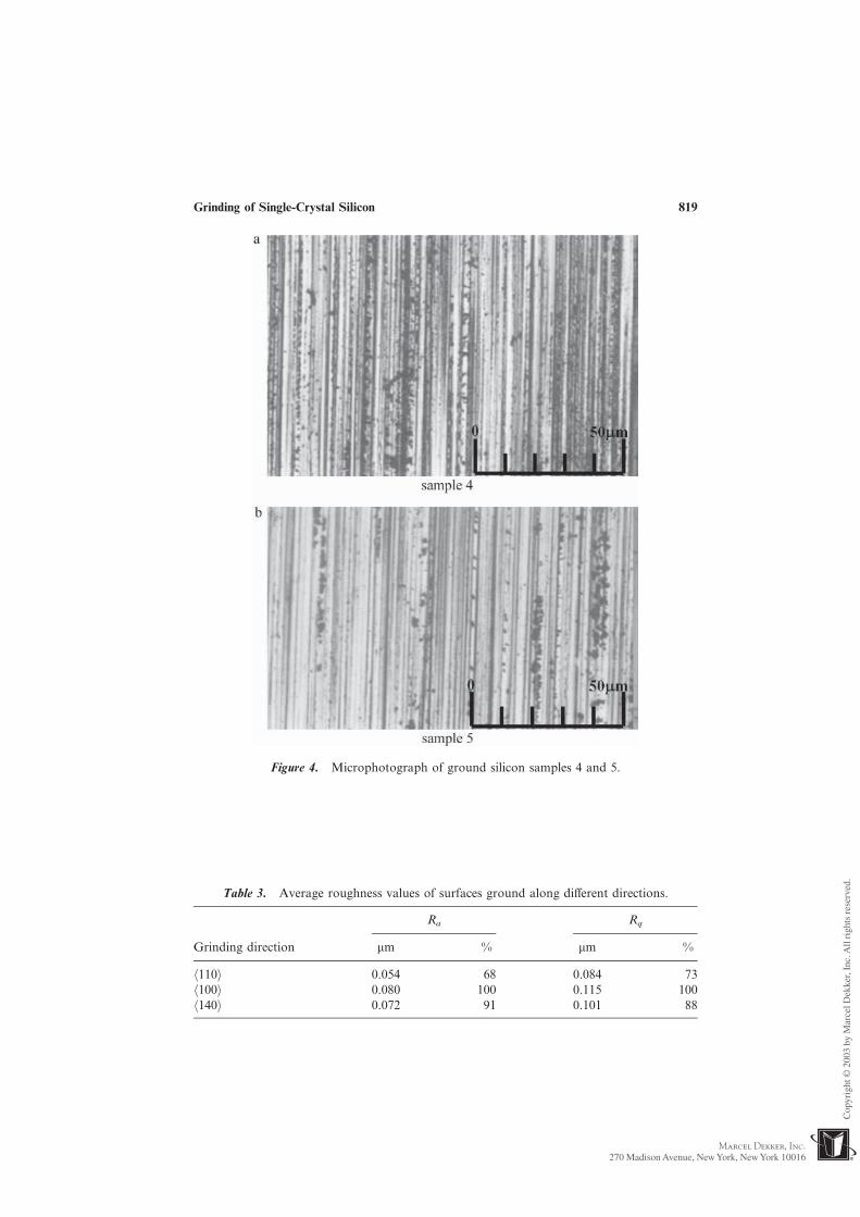
Table 3. Average roughness values of surfaces ground along different directions.
Ra Rq
Grinding direction mm % mm %
h110i 0.054 68 0.084 73h100i 0.080 100 0.115 100h140i 0.072 91 0.101 88
Figure 4. Microphotograph of ground silicon samples 4 and 5.
Grinding of Single-Crystal Silicon 819
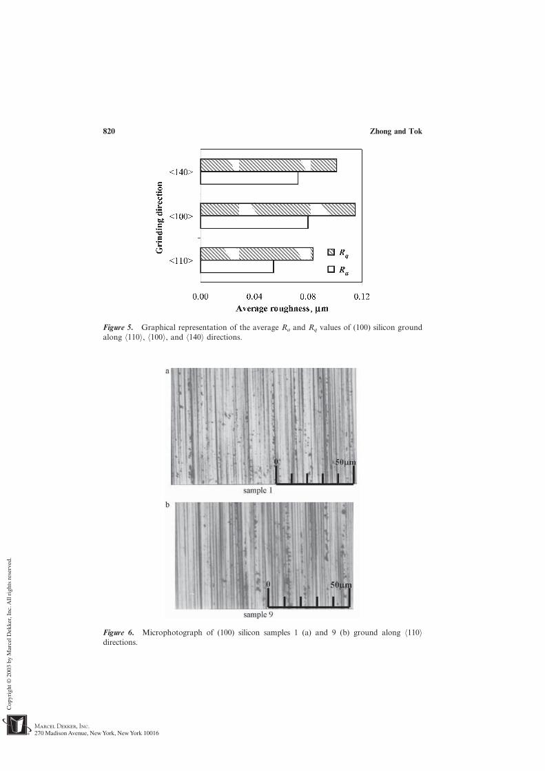
Figure 5. Graphical representation of the average Ra and Rq values of (100) silicon groundalong h110i, h100i, and h140i directions.
Figure 6. Microphotograph of (100) silicon samples 1 (a) and 9 (b) ground along h110idirections.
820 Zhong and Tok
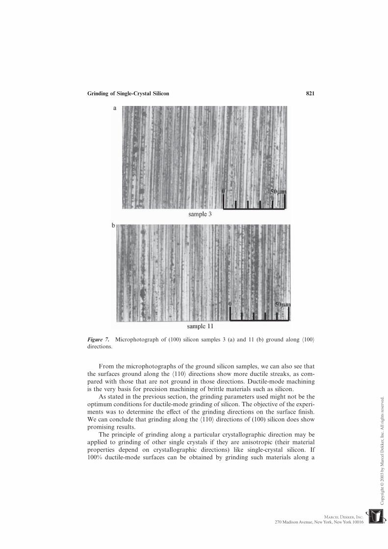
From the microphotographs of the ground silicon samples, we can also see thatthe surfaces ground along the h110i directions show more ductile streaks, as com-pared with those that are not ground in those directions. Ductile-mode machiningis the very basis for precision machining of brittle materials such as silicon.
As stated in the previous section, the grinding parameters used might not be theoptimum conditions for ductile-mode grinding of silicon. The objective of the experi-ments was to determine the effect of the grinding directions on the surface finish.We can conclude that grinding along the h110i directions of (100) silicon does showpromising results.
The principle of grinding along a particular crystallographic direction may beapplied to grinding of other single crystals if they are anisotropic (their materialproperties depend on crystallographic directions) like single-crystal silicon. If100% ductile-mode surfaces can be obtained by grinding such materials along a
Figure 7. Microphotograph of (100) silicon samples 3 (a) and 11 (b) ground along h100idirections.
Grinding of Single-Crystal Silicon 821
particular crystallographic direction, lapping and polishing are not required to pro-duce mirror surfaces. Even if only partial ductile-mode surfaces can be obtainedusing this method, the polishing time required to produce mirror surfaces can beshortened, because grinding along a particular crystallographic direction can pro-duce more ductile streaks than grinding along other directions and more ductilestreaks help reduce the polishing time needed. Therefore, this method can be com-mercially useful. Further research can be carried out to verify this point of view.
CONCLUSION
Results from the experiments of grinding along crystallographic orientations ofsingle-crystal (100) silicon suggested that better surface finish could indeed be
Figure 8. Microphotograph of (100) silicon samples 8 (a) and 14 (b) ground along h140idirections.
822 Zhong and Tok
achieved by grinding along h110i directions. The microphotographs also showedmore ductile streaks on the silicon surfaces ground along these directions, comparedwith the surfaces ground along the other directions.
REFERENCES
1. Gise, P.; Blanchard, R. Modern Semiconductor Fabrication Technology;Prentice-Hall: Englewood Cliffs, New Jersey, 1986.
2. Hsu, T.-R. MEMS & Microsystems: Design and Manufacture; McGraw-Hill:New York, 2002.
3. O’Mara, W.C.; Herring, R.B.; Hunt, L.P. Handbook of Semiconductor SiliconTechnology; Noyes Publications: Park Ridge, New Jersey, 1990.
4. Landers, T.L.; Brown, W.D.; Fant, E.W.; Malstrom, E.M.; Schmitt, N.M.Electronics Manufacturing Processes; Prentice-Hall: Englewood Cliffs, NewJersey, 1994.
5. Gardner, J.W.; Varadan, V.K.; Awadelkarim, O.O. Microsensors, MEMS, andSmart Devices; John Wiley & Sons, Inc.: Chichester, England, 2001.
6. Zhong, Z.; Venkatesh, V.C. Generation of parabolic and toroidal surfaces onsilicon and silicon based compounds using diamond cup grinding wheels.Annals of CIRP 1994, 43 (1), 323–326.
7. Iyer, S.S.; Auberton-Herve, A.J. Silicon Wafer Bonding Technology for VLSIand MEMS Applications; The Institution of Electrical Engineers: London,UK, 2002.
8. Venkatesh, V.C.; Inasaki, I.; Toenshof, H.K.; Nakagawa, T.; Marinescu, I.D.Observation on polishing and ultraprecison machining of semi-conductorsubstrate. Annals of the CIRP 1995, 44 (2), 611–618.
9. Toenshoff, H.K.; Schmieden, W.V.; Inasaki, I.; Konig, W.; Spur, G. Abrasivemachining of silicon. Annals of CIRP 1990, 39 (2), 621–635.
10. Zhang, B.; Howes, T.D. Material-removal mechanism in grinding ceramics.Annals of CIRP 1994, 43 (1), 305–308.
11. Kimimura, Y.; Yamaguchi, H.; Tani, Y. Ductile regime cutting of brittle mate-rials using a flying tool under negative pressure. Annals of CIRP 1997, 46 (1),451–454.
12. Shibata, T.; Fujii, S.; Makino, E.; Ikeda, M. Ductile-regime turning mechanismof single-crystal silicon. Precision Engineering 1996, 18, 129–137.
13. Suwabe, H.; Ishikawa, K.; Uneda, M. Effect of vibration using ultrasonicad low frequency vibration on grooving process for hard and brittle materials.Precision Engineering 1996, 14, 542–545.
14. Zhong, Z. New grinding methods for aspheric mirrors with large curvatureradii. Annals of CIRP 1992, 41 (1), 355–338.
15. Zhong, Z.W. Grinding of toroidal and cylindrical surfaces on SiC usingdiamond grinding wheels. Journal of Materials and Manufacturing Processes1997, 12 (6), 1049–1062.
16. Gatzen, H.H.; Maetzig, J.C. Nanogrinding. Precision Engineering 1997, 21,134–139.
Grinding of Single-Crystal Silicon 823
17. Tomita, Y.; Eda, H.; Yamamoto, Y.; Nakamura, M. Study of ultra precisionprocessing of silicon wafer by grinding stone. Precision Engineering 1995, 19,17–20.
18. Tani, T.; Saeki, T.; Samitsu, Y.; Kobayashi, K.; Sato, Y. Infeed grinding ofsilicon wafers applying electrophoretic deposition of ultrafine abrasive.Annals of CIRP 1998, 47 (1), 285–288.
19. Zhong, Z.W.; Lee, W.Y. Grinding of silicon and glass using a new dressingdevice and an improved coolant system. Journal of Materials and Manufactur-ing Processes 2001, 16 (4), 471– 482.
20. Hirao, M.; Izawa, M.; Iguchi, N.; Shirase, K.; Ootani, K.; Yasui, T. WaterjetIn-process dressing. Precision Engineering 1999, 20, 95–98.
21. Wang, X.; Ying, B.; Liu, W. EDM dressing of fine grain super abrasive grind-ing wheel. Precision Engineering 1995, 19, 5–8.
22. Callister, W.D., Jr. Materials Science and Engineering, 4th Ed.; John Wiley &Sons, Inc.: New York, 1997.
23. Van Vlack, L.H. Elements of Materials Science and Engineering, 6th Ed.; Addi-son-Wesley, 1989.
24. Hammond, C. Introduction to Crystallography; Oxford Science Publication,1990.
25. Maluf, N. An Introduction to Microelectromechanical System Engineering;Artech House: Norwood, MA, 2000.
26. Shimura, F. Semiconductor Silicon Crystal Technology; Academic Press: SanDiego, 1989.
824 Zhong and Tok