Embed Size (px)
Citation preview
GROWTH AND RAMAN SCATTERING CHARACTERIZATION OF Cu2ZnSnS4 THIN FILMS
P.A. Fernandes1,2, P.M.P. Salomé1, A.F. da Cunha1
1Departamento de Física, Universidade de Aveiro, Campus Universitário de Santiago, 3810-193
Aveiro, Portugal
2Departamento de Física, Instituto Superior de Engenharia do Porto, Instituto Politécnico do Porto,
Rua Dr. António Bernardino de Almeida, 431, 4200-072 Porto, Portugal
Abstract:
In the present work we report the results of the growth, morphological and structural characterization
of Cu2ZnSnS4 (CZTS) thin films prepared by sulfurization of DC magnetron sputtered Cu/Zn/Sn
precursor layers. The adjustment of the thicknesses and the properties of the precursors were used
to control the final composition of the films. Its properties were studied by SEM/EDS, XRD and
Raman scattering. The influence of the sulfurization temperature on the morphology, composition and
structure of the films has been studied. With the presented method we have been able to prepare
CZTS thin films with a kesterite structure.
Keywords: Cu2ZnSnS4, CZTS, sputtering, sulfurization, thin film, solar cell, Raman
1. Introduction
Nowadays best thin film solar cells maximum efficiencies are approaching mono-crystalline Si-
based ones [1]. Despite that, these still use rare and expensive materials like In, Ga and Te, they also
use toxic elements like Cd and Se, which represent a disadvantage. Cu2ZnSnS4 (CZTS) can be a
good choice for a new absorber layer presenting an absorption coefficient over 104 cm-1 and a band-
gap energy near 1.45 eV [2]. Several procedures have already been studied for the growth of CZTS.
Thermal evaporation was tested by T. Friedlmeier et al. [3]. E-Beam evaporation with a post
sulfurization process was studied by Takagiri et al. [4]. K. Jimbo et al. were successful in growing
CZTS using RF co-sputtering of binary compounds [5]. Routes using co-evaporated elements were
developed by T. Tanaka et al. [6]. So far the highest efficiency reported for CZTS solar cells is 5.7%
and it was achieved by K. Jimbo et al. [5]. Non vacuum methods have also been developed, namely
sulfurization of sol-gel deposited precursors by K. Tanaka et al. and spray-pyrolysis by N. Nakayama
et al. and N. Kamoun et al. [7 - 9].
In this work we study a two step method to grow CZTS. This method uses a sequential
deposition of metallic precursors by DC magnetron sputtering on soda lime glass (SLG) coated with
Mo. These layers are then heated up in a Sulphur (S) + Nitrogen gas (N2) atmosphere.
2. Experimental Details
2.1. Sample Preparation
The method used in this work can be divided in two stages. First, a sequential deposition of the
metallic precursor layers is performed by DC magnetron sputtering. The second stage is the
formation of the CZTS layer by sulfurization of the precursors.
The sample preparation process begins with the substrate cleaning, a 9 cm2 SLG, with
successive ultrasound baths of acetone/alcohol/deionised water. This step ends with substrate being
dried with a N2 flow. The back contact layer is a Mo bilayer deposited by DC magnetron sputtering
(target purity 99.95%). The deposition conditions followed the recipe developed by J. Scofield et al. to
ensure both low resistivity and good adhesion to the SLG [10]. A sequential deposition of metallic
precursors was performed using an Ar atmosphere and an operating pressure of 2×10⁻³ mbar. The
deposition order was Cu (target purity 99.999%), Zn (target purity 99.99%) and finally Sn (target
purity 99.99%). Several deposition power settings were used with the following values 0.16 Wcm-2,
0.16-0.38 Wcm-2, 0.11-0.16 Wcm-2 for Cu, Zn and Sn, respectively. The individual thicknesses were
estimated using the density and molecular weight of each element. In situ monitoring of the layer
thicknesses was done with a quartz crystal monitor.
For the second stage, which refers to CZTS formation, a temperature controlled tubular
furnace, was used. The sample was heated in a N2 atmosphere at an operating pressure of 5.6×10⁻¹
mbar. The sample heating rate was 10 ºC/min. The sulfurization temperature profile, for a maximum
temperature of 525 ºC, is sketched in figure 1. In this stage the only parameter changed, between
samples, was the maximum sulfurization temperature. The Sulphur evaporation source was a quartz
tube filled with elemental Sulphur pellets (purity 99.999%). The evaporation temperature was 130 ºC
and the N2 flow rate was 40 ml/min.
2.2. Characterization
Confirmation of individual metallic precursor layer and CZTS thicknesses was done using stylus
profilometry technique with a Veeco Dektak 150 surface profiler. The structural analysis of the CZTS
thin films was done by X-ray diffraction on a PHILIPS PW 3710 device equipped with a Cu-Kα source
(wavelength λ=1.54060 Å) and the generator settings were 50 mA, 40 kV. The SEM/EDS systems
used were a SEM Hitachi S4100 and a Rontec EDS with setting parameters of 25 KeV and 10 µA for
surface imaging and a Hitachi SU-70 with a Quantax Bruker AXS EDS system with 15/25 KeV and 40
µA for cross-section imaging. For Raman spectroscopy, the LASER line used was 514.5 nm and the
device was a Jobin-Yvon T64000.
3. Results and Discussion
Since there is a lack of information on the thermodynamics of CZTS thin film formation, the
initial study was aimed at clarifying this issue. The second study was a detailed analysis of the best
CZTS samples.
In this approach all the metallic precursor thicknesses were kept constant with the following
values, Cu-150 nm, Zn-190 nm and Sn-340 nm. The sulfurization temperatures were 330 ºC, 370 ºC,
425 ºC and 505 ºC. This parameter was used to name the various samples. The EDS analysis
showed that all samples had an excess of Sn and an average concentration ratio of 0.87 and 0.40 for
[Cu]/([Zn]+[Sn]) and [Zn]/[Sn], respectively. The results of Raman scattering and XRD analysis are
presented in figure 2 and figure 3, respectively. For the sample S330, the Raman spectra shows
evidence of the presence of SnS with characteristic modes at 160 cm-1, 190 cm-1, 220 cm-1 and SnS2
with a mode at 315 cm-1 this assignment of the peaks is in agreement with data reported by other
authors [11]. XRD analysis confirmed the presence of the binary compounds. The Raman analysis for
sample S370 only shows the existence of SnS2 peak at 315 cm-1. Again XRD data provides a
confirmation of the presence of SnS2. In both samples, XRD analysis detected elemental Zn. For
S425 the Raman scattering analysis shows major peaks, at 264 cm-1, 304 cm-1 and 356 cm-1
corresponding to Cu2-xS [12], Sn2S3 [11] and cubic ZnS [13], respectively. This sample’s XRD pattern
matches the peaks of β-ZnS according to [14]. Note that the spectra of CZTS and β-ZnS are very
similar for visible peaks and the angle differences are within the instrument accuracy. There can be
also some stress-related shifts that might cause changes of this magnitude. These facts turn the XRD
identification of CZTS a difficult task. For sample S505, the Raman characterization shows a single
peak at 338 cm-1. XRD analysis shows both ZnS and CZTS to be present. Since there is almost no
cubic ZnS Raman peak and the only published data of Raman is for monograins not for thin films we
have associated the 338cm-1 peak to CZTS [15]. This fact reveals the importance of Raman analysis
to distinguish between β-ZnS and CZTS.
Using the results just discussed we have increased the sulfurization temperature to 525 ºC and
corrected the chemical composition of the precursors. EDS analysis was used to determine chemical
composition of metallic precursors and CZTS. The element concentration ratio is shown in table 1.
From this table it can be observed that the sulfurization process causes a loss in Zn concentration.
Although it is not observed in these results, a small loss of Sn also occurs in most cases. It can be
explained by evaporation of these two elements during the heating process under vacuum.
From the XRD pattern, figure 4, it can be observed the presence of CZTS with a preferential
growth orientation of (112). The sharpness of the major peaks indicates a good crystallinity. These
results have also confirmed the presence of binary chalcogenides, such as sphalerite ZnS and
covellite Cu2-xS. The figure 5 shows the results of Raman scattering in two zones of the sample S525.
The existence of CZTS is confirmed by the presence of Raman peaks at 338-339 cm-1, 288 cm-1 and
256-257 cm-1. These are in agreement with the published data for monograins of CZTS [15]. Zone 1
show a strong peak for Cu2-xS at 476 cm-1 which is not observed in zone 2 [12]. The spectra of both
zones exhibit a shoulder at 255 cm-1, which is believed to be the convolution of peaks corresponding
to Sn2S3, CZTS, Cu2-xS and ZnS [11-15]. ZnS is also detected with Raman analysis with peaks
located at 348 cm-1 [13].
The morphology and grain size was analysed using a SEM and the results are presented in
figure 6 and 7. Figure 6 shows good crystallinity and compactness of the CZTS layer. The surface
shows some roughness and few voids. Figure 7 shows sparse large grains that have been identified
as Cu2-xS crystallites. Their composition was confirmed with EDS analysis. Figure 8 shows the cross
section SEM image of the S525 with layer thickness indication. It shows that the CZTS layer has a
thickness of 1.5 μm. It can be observed a void or cavity between the CZTS and the Mo layer which
could be created either during the film growth or during the cutting process. Nevertheless, these
pictures show a compact CZTS layer and confirm the presence of Cu2-xS situated at the top of the
film.
4. Conclusions
This work shows that it is possible to grow the Cu2ZnSnS4 absorber layer with this two-step
procedure. Further research must be carried out to optimize the film quality, to produce a more
compact layer and to improve the adhesion of the absorber layer to the back-contact. The elimination
of Cu2-xS phases may be performed using a more accurate composition control of the metallic
precursors and/or a chemical surface treatment with KCN.
It was also proved that, since in XRD analysis it is difficult to distinguish between ZnS and
CZTS, Raman analysis is an important and a complementary analysis method. The thin film CZTS
Raman modes appear at the same wavenumbers as those of monograin CZTS.
5. Bibliography:
[1] Ingrid Repins, M. Contreras, B. Egaas, C.DeHart, J. Scharf, C.Perkins, B. To and R. Noufi, Prog.
in Photovolt.: Research and Applications, Volume 16, Issue 3 , Pages 235 – 239.
[2] J.M. Raulot, C. Domain , J.F. Guillemoles, Journal of Physics and Chemistry of Solids 66 (2005)
2019–2023.
[3] Th. Friedlmeier, N. Wieser, Th. Walter, H. Dittrich, H.-W. Schock, Proceedings of the 14th
European PVSEC and Exhibition, 1997, P4B.10.
[4] H. Katagiri, K. Saitoh, T. Washio, H. Shinohara, T. Kurumadani, S. Miyajima, Solar Energy
Materials and Solar Cells, Volume 65, Issues 1-4, January 2001, Pages 141-148.
[5] KK. Jimbo, R. Kimura, T. Kamimura, S. Yamada, W. Maw, H. Araki, K. Oishi, H. Katagiri, Thin
Solid Films, Volume 515, Issue 15, 31 May 2007, Pages 5997-5999.
[6] T. Tanaka, D. Kawasaki, M. Nishio, Q. Guo, H. Ogawa, Phys. Stat. sol. (c) 3, No. 8, 2844-2847
(2006).
[7] K. Tanaka, N. Moritake, H. Uchiki, Solar Energy Materials and Solar Cells, Volume 91, Issue 13,
15 August 2007, Pages 1199-1201.
[8] N. Nakayama and K. Ito, Applied Surface Science, vol. 92, pp. 171-175, 1996.
[9] N. Kamoun, H. Bouzouita, B. Rezig, Thin Solid Films, Volume 515, Issue 15, 31 May 2007, Pages
5949-5952.
[10] John H. Scofield, A. Duda, D. Albin, B. L. Ballard, P. K. Predecki, Thin Solid Films, Volume 260,
Issue 1, 1 May 1995, Pages 26-31.
[11] I. P. Parkin, L. S. Price, T. G. Hibbertb and K. C. Molloyb, J. Mater. Chem., 2001, 11, 1486–
1490.
[12] Carolyn G. Muncea, Gretel K. Parker a, Stephen A. Holt b, Gregory A. Hopea, Colloids and
Surfaces A: Physicochem. Eng. Aspects 295 (2007) 152–158.
[13] J. Serrano, A. Cantarero, M. Cardona, N. Garro, R. Lauck, R. E. Tallman, T. M. Ritter and B. A.
Weinstein, PHYSICAL REVIEW B 69, 014301, 2004.
[14] International Centre for Diffraction Data, 14 04-005-0388 (CZTS), 04-004-3804 (Cubic ZnS), 04-
004-3831 (Orthorhombic-Sns), 04-003-4154 (Hexagonal - SnS2), 04-001-1461 (Hexagonal –
CuS).
[15] M. Altosaar, J. Raudoja, K. Timmo, M. Danilson, M. Grossberg, J. Krustok, and E. Mellikov, p
hys. stat. sol. (a) 205, No. 1, 167–170 (2008)

Precursor metallic layers (before sulfurization) CZTS (after sulfurization)
Composition ratio Composition ratio
[Cu]/([Zn]+[Sn]) [Zn]/[Sn] [Cu]/([Zn]+[Sn]) [Zn]/[Sn] Metal/S
0.87 1.09 0.90 0.87 1.03
Table 1: Composition ratios for metallic precursor layers and CZTS.
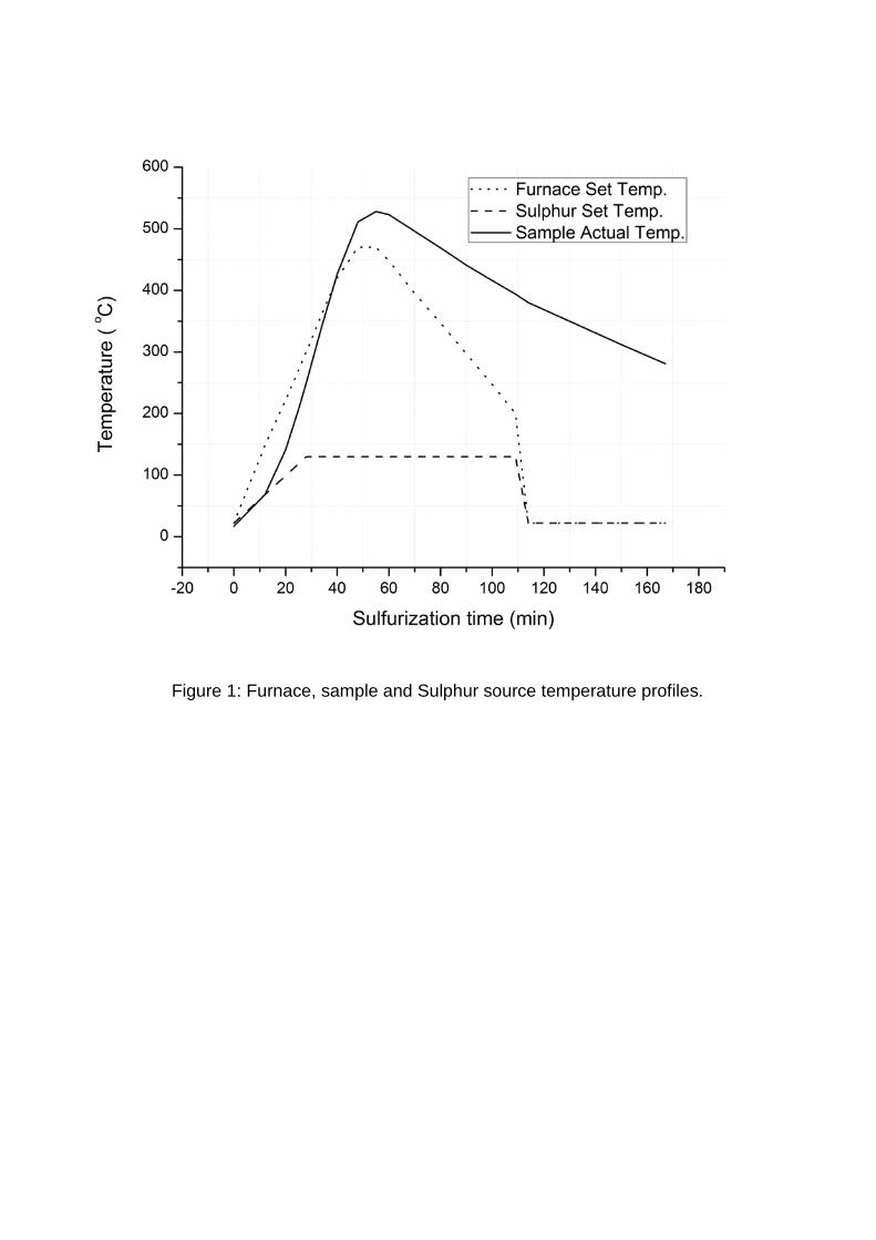
Figure 1: Furnace, sample and Sulphur source temperature profiles.
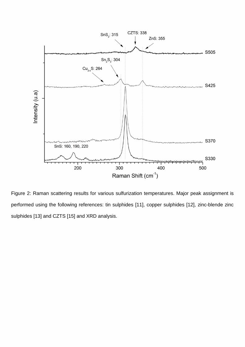
Figure 2: Raman scattering results for various sulfurization temperatures. Major peak assignment is
performed using the following references: tin sulphides [11], copper sulphides [12], zinc-blende zinc
sulphides [13] and CZTS [15] and XRD analysis.
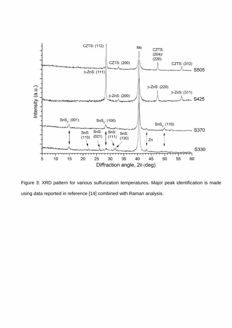
Figure 3: XRD pattern for various sulfurization temperatures. Major peak identification is made
using data reported in reference [14] combined with Raman analysis.
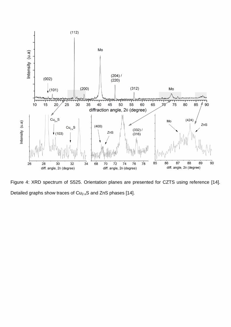
Figure 4: XRD spectrum of S525. Orientation planes are presented for CZTS using reference [14].
Detailed graphs show traces of Cu2-xS and ZnS phases [14].
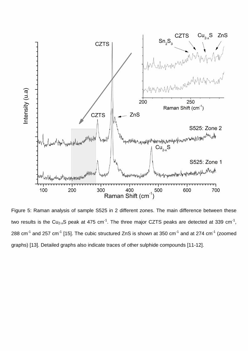
Figure 5: Raman analysis of sample S525 in 2 different zones. The main difference between these
two results is the Cu2-xS peak at 475 cm-1. The three major CZTS peaks are detected at 339 cm-1,
288 cm-1 and 257 cm-1 [15]. The cubic structured ZnS is shown at 350 cm-1 and at 274 cm-1 (zoomed
graphs) [13]. Detailed graphs also indicate traces of other sulphide compounds [11-12].
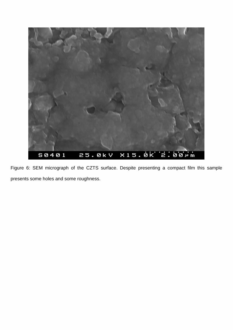
Figure 6: SEM micrograph of the CZTS surface. Despite presenting a compact film this sample
presents some holes and some roughness.
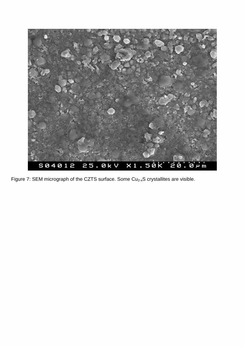
Figure 7: SEM micrograph of the CZTS surface. Some Cu2-xS crystallites are visible.
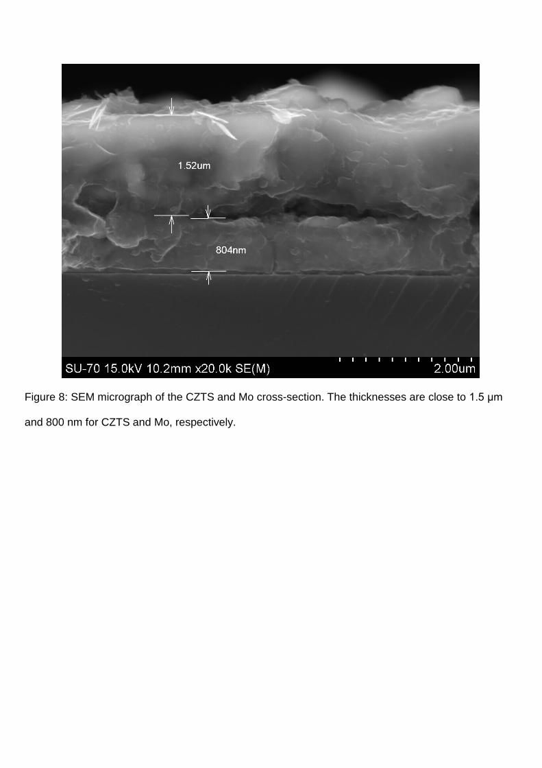
Figure 8: SEM micrograph of the CZTS and Mo cross-section. The thicknesses are close to 1.5 μm
and 800 nm for CZTS and Mo, respectively.