Embed Size (px)
Citation preview
Delivered by Ingenta toSung Kyun Kwan University
IP 11514516612Wed 25 Jul 2012 130745
RESEARCH
ARTIC
LE
Copyright copy 2012 American Scientific PublishersAll rights reservedPrinted in the United States of America
Journal ofNanoscience and Nanotechnology
Vol 12 1551ndash1554 2012
Growth of High Quality ZnO Nanowires on Graphene
Keun Young Lee1 Brijesh Kumar1 Hyun-Kyu Park1 Won Mook Choi3Jae-Young Choi3 and Sang-Woo Kim12lowast
1School of Advanced Materials Science and Engineering Sungkyunkwan University Suwon 440-746 Republic of Korea2SKKU Advanced Institute of Nanotechnology (SAINT) and Center for Human Interface Nanotechnology (HINT)
Sungkyunkwan University Suwon 440-746 Republic of Korea3Samsung Advanced Institute of Technology Yongin Gyeonggi 446-712 Republic of Korea
We report growth of the ZnO nanowires on grapheneSiO2Si substrates using a chemical vapordeposition method The length of nanowires varies from 1 m to 10 m with increasing the growthtime from 30 min to 90 min X-ray diffraction and high-resolution transmission electron microscopyinvestigations predict the high structural quality of the c-axis grown single crystalline ZnO nanowiresTemperature dependent photoluminescence spectra from the nanowires reveal excellent opticalquality and excitonic behavior in the single crystalline ZnO nanowires A well-resolved free excitonemission at 3375 eV indicates high crystalline quality nanowires and a strong PL peak at 3370 eVis assigned to neutral-donor bound excitons (D0X)
Keywords Graphene ZnO Nanowires PL Free Exciton
1 INTRODUCTION
Two-dimensional graphene sheets are of particular inter-est because of their extraordinary electrical thermaland mechanical properties including carrier mobilityexceeding 104 cm2Vs and a thermal conductivity of103 WmK1ndash4 Graphene-based inorganic hybrid nano-structures including nanowires nanobelts nanospringsnanorings nanobows and nanohelices offer addi-tional functionality for realizing advanced nanoscaleelectronics and optoelectronics applications in photo-voltaics nanogenerators and field emission devices56
When incorporated into polymer or ceramic matricesgraphene can remarkably improve the properties of thesehost materials7ndash10 Recently several grapheneinorganicnanocomposites have been successfully synthesized thatshow desirable combinations of these properties not foundin the individual components11ndash16
Quasi-one-dimensional zinc oxide (ZnO) semi-conducting nanostructures that have extremely largesurface-to-volume ratios are considered to be importantmultifunctional building blocks for fabricating variousnanodevices1718 Owing to their unique electronic andoptical properties ZnO nanostructures have been suc-cessfully applied in field effect transistors light-emittingdiodes laser diodes sensors and resonators Semicon-ductor nanostructures grown on graphene sheets enable
lowastAuthor to whom correspondence should be addressed
their novel physical properties to be exploited in diversesophisticated device applications This paper reports thegrowth of highly crystalline high optical quality ZnOnanowires on graphene substrates by chemical vapordeposition (CVD) X-ray diffraction (XRD) results revealthe excellent structural quality of the nanowires Temper-ature dependent photoluminescence (PL) spectra of thenanowires reveal excellent optical quality and excitonicbehavior in the c-axis grown crystalline nanowires
2 EXPERIMENTAL PROCEDURES
21 Fabrication Process of Graphene
Large-scale graphene sheets were synthesized by a CVDmethod51920 First copper (Cu) foil was placed in a ther-mal CVD chamber and the temperature was increasedfrom room temperature to 1000 C for 250 minutes undera hydrogen (H2 gas flow rate at 10 standard cubic cen-timeters per minute (sccm) Then the gas mixing ratioof methane (CH4 to H2 was 510 sccm for synthesis ofgraphene sheets over a growth time of 30 minutes Aftergrowth was completed the CH4 gas supply was termi-nated and the chamber was cooled down to 500 C at acooling rate of 160 C minminus1 with a H2 gas flow rate of10 sccm Further graphene sheets were separated from theCu foil using a Cu etchant Separated floating graphenesheets were then transferred to 300 nm thick silicon diox-ide (SiO2 deposited on silicon (Si) substrate using the
J Nanosci Nanotechnol 2012 Vol 12 No 2 1533-48802012121551004 doi101166jnn20124627 1551
Delivered by Ingenta toSung Kyun Kwan University
IP 11514516612Wed 25 Jul 2012 130745
RESEARCH
ARTIC
LE
Growth of High Quality ZnO Nanowires on Graphene Lee et al
fishing method19 The transferred graphene sheets wereused as platforms for ZnO nanowire growth
22 Synthesis of ZnO Nanowires
ZnO nanowires were grown by thermal CVD by vapor-izing the mixed ZnO and graphite (11) powder A gold(Au) layer with a thickness of 2 nm was coated ontothe grapheneSiO2Si substrates as a catalyst to grow ZnOnanowires by thermal evaporation The source powder andAu-coated substrates were placed in a ceramic boat andwere then loaded in the center of the tube The ZnOnanowires were synthesized at a temperature of 950 C for20 minutes under an argon gas flow rate (50 sccm)
23 Characterization
The morphology and structural properties of as-grownZnO nanowires were examined using field-emissionscanning electron microscopy (FE-SEM) high-resolutiontransmission electron microscopy (HRTEM) and XRDwith CuK radiation Optical properties were investigatedby PL measurements using a 325 nm He-Cd laser as anexcitation source
3 RESULTS AND DISCUSSION
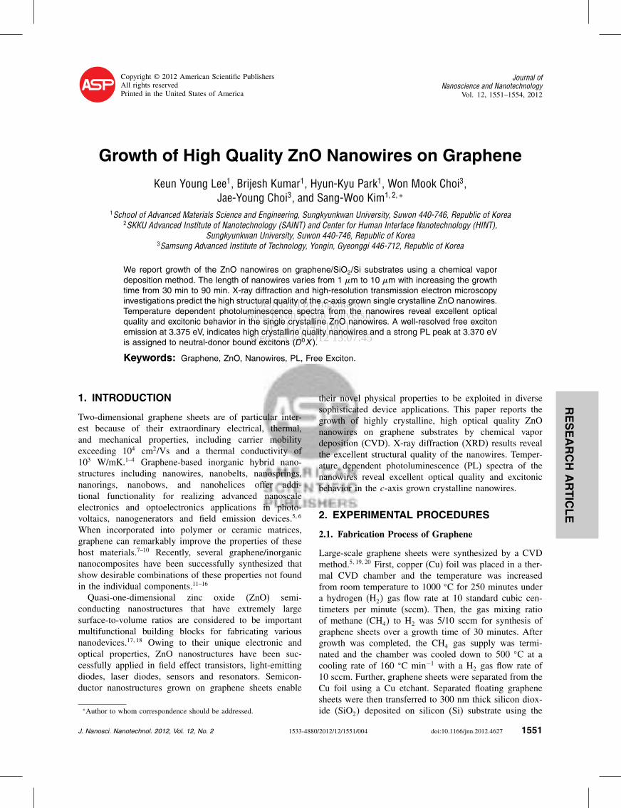
Figure 1(a) shows the Raman spectra of thegrapheneSiO2Si layers exhibiting G and 2D modesThe strongly suppressed defect-related D-band peakverifies the good overall quality of the graphene sheetused for ZnO nanowire growth Figures 1(bndashd) showFE-SEM images of ZnO nanowires that were grown onthe grapheneSiO2Si substrate The surface morphologiesof the ZnO nanowires vary with increasing growth timefrom 30 minutes to 90 minutes As shown in Figure 1(b)after 30 minutes ZnO nucleates and forms a transitionlayer with a height of about 200 nm On the transitionlayer a few low density nanowires grow concurrently inthis initial stage without a preferential orientation Theaverage length of the nanowires was about 1 m whilethe diameter was below 20 nmThe low density is likely responsible for the poor orien-
tation After the transition layer is formed on the substrateperpendicular nanowire growth dominates the processZnO nanowires grow with high growth rate in the directionof the c-axis as this is the direction of the lowest surfaceenergy Therefore nanowires that nucleate with the c-axisperpendicular to the substrate surface can eventually growinto long nanowires while other nucleation sites alongthe substrate surface having an inclined angle will stopgrowing when c-axis nanowires grow long enough Con-sequently only c-axis single crystalline nanowires domi-nate ZnO nanowires growth This phenomenon causes thenanowire density to be less than the nucleation density
Fig 1 (a) Raman spectrum of graphene sheets deposited on SiO2Sisubstrates and FE-SEM images of Zno nanowires grown on graphene for(b) 30 minutes (c) 60 minutes and (D) 90 minutes
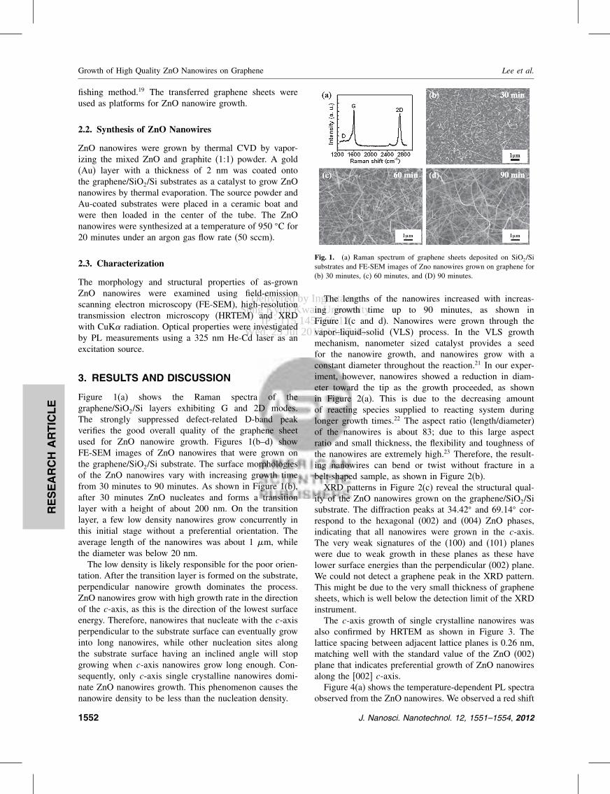
The lengths of the nanowires increased with increas-ing growth time up to 90 minutes as shown inFigure 1(c and d) Nanowires were grown through thevaporndashliquidndashsolid (VLS) process In the VLS growthmechanism nanometer sized catalyst provides a seedfor the nanowire growth and nanowires grow with aconstant diameter throughout the reaction21 In our exper-iment however nanowires showed a reduction in diam-eter toward the tip as the growth proceeded as shownin Figure 2(a) This is due to the decreasing amountof reacting species supplied to reacting system duringlonger growth times22 The aspect ratio (lengthdiameter)of the nanowires is about 83 due to this large aspectratio and small thickness the flexibility and toughness ofthe nanowires are extremely high23 Therefore the result-ing nanowires can bend or twist without fracture in abelt-shaped sample as shown in Figure 2(b)XRD patterns in Figure 2(c) reveal the structural qual-
ity of the ZnO nanowires grown on the grapheneSiO2Sisubstrate The diffraction peaks at 3442 and 6914 cor-respond to the hexagonal (002) and (004) ZnO phasesindicating that all nanowires were grown in the c-axisThe very weak signatures of the (100) and (101) planeswere due to weak growth in these planes as these havelower surface energies than the perpendicular (002) planeWe could not detect a graphene peak in the XRD patternThis might be due to the very small thickness of graphenesheets which is well below the detection limit of the XRDinstrumentThe c-axis growth of single crystalline nanowires was
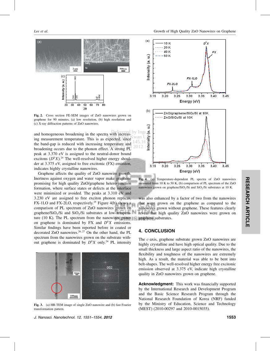
also confirmed by HRTEM as shown in Figure 3 Thelattice spacing between adjacent lattice planes is 026 nmmatching well with the standard value of the ZnO (002)plane that indicates preferential growth of ZnO nanowiresalong the [002] c-axisFigure 4(a) shows the temperature-dependent PL spectra
observed from the ZnO nanowires We observed a red shift
1552 J Nanosci Nanotechnol 12 1551ndash1554 2012
Delivered by Ingenta toSung Kyun Kwan University
IP 11514516612Wed 25 Jul 2012 130745
RESEARCH
ARTIC
LE
Lee et al Growth of High Quality ZnO Nanowires on Graphene
Fig 2 Cross section FE-SEM images of ZnO nanowires grown ongraphene for 90 minutes (a) low resolution (b) high resolution and(c) X-ray diffraction patterns of ZnO nanowires
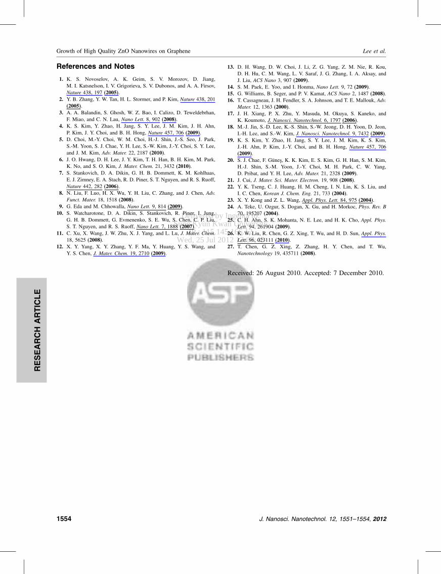
and homogeneous broadening in the spectra with increas-ing measurement temperature This is as expected sincethe band-gap is reduced with increasing temperature andbroadening occurs due to the phonon effect A strong PLpeak at 3370 eV is assigned to the neutral-donor boundexcitons (D0X)24 The well-resolved higher energy shoul-der at 3375 eV assigned to free excitonic (FX) emissionindicates highly crystalline nanowiresGraphene affects the quality of ZnO nanowire growth
Inertness against oxygen and water vapor make graphenepromising for high quality ZnOgraphene hetero-junctionformation where surface states or defects at the interfacewere minimized or avoided The peaks at 3310 eV and3230 eV are assigned to free exciton phonon replicasFX-1LO and FX-2LO respectively25 Figure 4(b) shows acomparison of PL spectrum of ZnO nanowires grown ongrapheneSiO2Si and SiO2Si substrates at low tempera-ture (10 K) The PL spectrum from the nanowires grownon graphene is dominated by FX and D0X emissionsSimilar findings have been reported before in coated ordecorated ZnO nanowires2627 On the other hand the PLspectrum from the nanowires grown on the substrate with-out graphene is dominated by D0X only24 PL intensity
Fig 3 (a) HR-TEM image of single ZnO nanowire and (b) fast Fouriertransformation pattern
Fig 4 (a) Temperature-dependent PL spectra of ZnO nanowiresmeasured from 10 K to 50 K (b) comparison of PL spectrum of the ZnOnanowires grown on grapheneSiO2Si and SiO2Si substrates at 10 K
was also enhanced by a factor of two from the nanowiresthat were grown on the graphene as compared to thenanowires grown without graphene These features clearlyreveal that high quality ZnO nanowires were grown ongraphene substrates
4 CONCLUSION
The c-axis graphene substrate grown ZnO nanowires arehighly crystalline and have high optical quality Due to thesmall thickness and large aspect ratio of the nanowires theflexibility and toughness of the nanowires are extremelyhigh As a result the material was able to be bent intobelt-shapes The well-resolved higher energy free excitonicemission observed at 3375 eV indicate high crystallinequality in ZnO nanowires grown on graphene
Acknowledgment This work was financially supportedby the International Research and Development Programand the Basic Science Research Program through theNational Research Foundation of Korea (NRF) fundedby the Ministry of Education Science and Technology(MEST) (2010-00297 and 2010-0015035)
J Nanosci Nanotechnol 12 1551ndash1554 2012 1553
Delivered by Ingenta toSung Kyun Kwan University
IP 11514516612Wed 25 Jul 2012 130745
RESEARCH
ARTIC
LE
Growth of High Quality ZnO Nanowires on Graphene Lee et al
References and Notes
1 K S Novoselov A K Geim S V Morozov D JiangM I Katsnelson I V Grigorieva S V Dubonos and A A FirsovNature 438 197 (2005)
2 Y B Zhang Y W Tan H L Stormer and P Kim Nature 438 201(2005)
3 A A Balandin S Ghosh W Z Bao I Calizo D TeweldebrhanF Miao and C N Lau Nano Lett 8 902 (2008)
4 K S Kim Y Zhao H Jang S Y Lee J M Kim J H AhnP Kim J Y Choi and B H Hong Nature 457 706 (2009)
5 D Choi M-Y Choi W M Choi H-J Shin J-S Seo J ParkS-M Yoon S J Chae Y H Lee S-W Kim J-Y Choi S Y Leeand J M Kim Adv Mater 22 2187 (2010)
6 J O Hwang D H Lee J Y Kim T H Han B H Kim M ParkK No and S O Kim J Mater Chem 21 3432 (2010)
7 S Stankovich D A Dikin G H B Dommett K M KohlhaasE J Zimney E A Stach R D Piner S T Nguyen and R S RuoffNature 442 282 (2006)
8 N Liu F Luo H X Wu Y H Liu C Zhang and J Chen AdvFunct Mater 18 1518 (2008)
9 G Eda and M Chhowalla Nano Lett 9 814 (2009)10 S Watcharotone D A Dikin S Stankovich R Piner I Jung
G H B Dommett G Evmenenko S E Wu S Chen C P LiuS T Nguyen and R S Ruoff Nano Lett 7 1888 (2007)
11 C Xu X Wang J W Zhu X J Yang and L Lu J Mater Chem18 5625 (2008)
12 X Y Yang X Y Zhang Y F Ma Y Huang Y S Wang andY S Chen J Mater Chem 19 2710 (2009)
13 D H Wang D W Choi J Li Z G Yang Z M Nie R KouD H Hu C M Wang L V Saraf J G Zhang I A Aksay andJ Liu ACS Nano 3 907 (2009)
14 S M Paek E Yoo and I Honma Nano Lett 9 72 (2009)15 G Williams B Seger and P V Kamat ACS Nano 2 1487 (2008)16 T Cassagneau J H Fendler S A Johnson and T E Mallouk Adv
Mater 12 1363 (2000)17 J H Xiang P X Zhu Y Masuda M Okuya S Kaneko and
K Koumoto J Nanosci Nanotechnol 6 1797 (2006)18 M-J Jin S-D Lee K-S Shin S-W Jeong D H Yoon D Jeon
I-H Lee and S-W Kim J Nanosci Nanotechnol 9 7432 (2009)19 K S Kim Y Zhao H Jang S Y Lee J M Kim K S Kim
J-H Ahn P Kim J-Y Choi and B H Hong Nature 457 706(2009)
20 S J Chae F Guumlnes K K Kim E S Kim G H Han S M KimH-J Shin S-M Yoon J-Y Choi M H Park C W YangD Pribat and Y H Lee Adv Mater 21 2328 (2009)
21 J Cui J Mater Sci Mater Electron 19 908 (2008)22 Y K Tseng C J Huang H M Cheng I N Lin K S Liu and
I C Chen Korean J Chem Eng 21 733 (2004)23 X Y Kong and Z L Wang Appl Phys Lett 84 975 (2004)24 A Teke U Ozgur S Dogan X Gu and H Morkoc Phys Rev B
70 195207 (2004)25 C H Ahn S K Mohanta N E Lee and H K Cho Appl Phys
Lett 94 261904 (2009)26 K W Liu R Chen G Z Xing T Wu and H D Sun Appl Phys
Lett 96 023111 (2010)27 T Chen G Z Xing Z Zhang H Y Chen and T Wu
Nanotechnology 19 435711 (2008)
Received 26 August 2010 Accepted 7 December 2010
1554 J Nanosci Nanotechnol 12 1551ndash1554 2012
Delivered by Ingenta toSung Kyun Kwan University
IP 11514516612Wed 25 Jul 2012 130745
RESEARCH
ARTIC
LE
Growth of High Quality ZnO Nanowires on Graphene Lee et al
fishing method19 The transferred graphene sheets wereused as platforms for ZnO nanowire growth
22 Synthesis of ZnO Nanowires
ZnO nanowires were grown by thermal CVD by vapor-izing the mixed ZnO and graphite (11) powder A gold(Au) layer with a thickness of 2 nm was coated ontothe grapheneSiO2Si substrates as a catalyst to grow ZnOnanowires by thermal evaporation The source powder andAu-coated substrates were placed in a ceramic boat andwere then loaded in the center of the tube The ZnOnanowires were synthesized at a temperature of 950 C for20 minutes under an argon gas flow rate (50 sccm)
23 Characterization
The morphology and structural properties of as-grownZnO nanowires were examined using field-emissionscanning electron microscopy (FE-SEM) high-resolutiontransmission electron microscopy (HRTEM) and XRDwith CuK radiation Optical properties were investigatedby PL measurements using a 325 nm He-Cd laser as anexcitation source
3 RESULTS AND DISCUSSION
Figure 1(a) shows the Raman spectra of thegrapheneSiO2Si layers exhibiting G and 2D modesThe strongly suppressed defect-related D-band peakverifies the good overall quality of the graphene sheetused for ZnO nanowire growth Figures 1(bndashd) showFE-SEM images of ZnO nanowires that were grown onthe grapheneSiO2Si substrate The surface morphologiesof the ZnO nanowires vary with increasing growth timefrom 30 minutes to 90 minutes As shown in Figure 1(b)after 30 minutes ZnO nucleates and forms a transitionlayer with a height of about 200 nm On the transitionlayer a few low density nanowires grow concurrently inthis initial stage without a preferential orientation Theaverage length of the nanowires was about 1 m whilethe diameter was below 20 nmThe low density is likely responsible for the poor orien-
tation After the transition layer is formed on the substrateperpendicular nanowire growth dominates the processZnO nanowires grow with high growth rate in the directionof the c-axis as this is the direction of the lowest surfaceenergy Therefore nanowires that nucleate with the c-axisperpendicular to the substrate surface can eventually growinto long nanowires while other nucleation sites alongthe substrate surface having an inclined angle will stopgrowing when c-axis nanowires grow long enough Con-sequently only c-axis single crystalline nanowires domi-nate ZnO nanowires growth This phenomenon causes thenanowire density to be less than the nucleation density
Fig 1 (a) Raman spectrum of graphene sheets deposited on SiO2Sisubstrates and FE-SEM images of Zno nanowires grown on graphene for(b) 30 minutes (c) 60 minutes and (D) 90 minutes
The lengths of the nanowires increased with increas-ing growth time up to 90 minutes as shown inFigure 1(c and d) Nanowires were grown through thevaporndashliquidndashsolid (VLS) process In the VLS growthmechanism nanometer sized catalyst provides a seedfor the nanowire growth and nanowires grow with aconstant diameter throughout the reaction21 In our exper-iment however nanowires showed a reduction in diam-eter toward the tip as the growth proceeded as shownin Figure 2(a) This is due to the decreasing amountof reacting species supplied to reacting system duringlonger growth times22 The aspect ratio (lengthdiameter)of the nanowires is about 83 due to this large aspectratio and small thickness the flexibility and toughness ofthe nanowires are extremely high23 Therefore the result-ing nanowires can bend or twist without fracture in abelt-shaped sample as shown in Figure 2(b)XRD patterns in Figure 2(c) reveal the structural qual-
ity of the ZnO nanowires grown on the grapheneSiO2Sisubstrate The diffraction peaks at 3442 and 6914 cor-respond to the hexagonal (002) and (004) ZnO phasesindicating that all nanowires were grown in the c-axisThe very weak signatures of the (100) and (101) planeswere due to weak growth in these planes as these havelower surface energies than the perpendicular (002) planeWe could not detect a graphene peak in the XRD patternThis might be due to the very small thickness of graphenesheets which is well below the detection limit of the XRDinstrumentThe c-axis growth of single crystalline nanowires was
also confirmed by HRTEM as shown in Figure 3 Thelattice spacing between adjacent lattice planes is 026 nmmatching well with the standard value of the ZnO (002)plane that indicates preferential growth of ZnO nanowiresalong the [002] c-axisFigure 4(a) shows the temperature-dependent PL spectra
observed from the ZnO nanowires We observed a red shift
1552 J Nanosci Nanotechnol 12 1551ndash1554 2012
Delivered by Ingenta toSung Kyun Kwan University
IP 11514516612Wed 25 Jul 2012 130745
RESEARCH
ARTIC
LE
Lee et al Growth of High Quality ZnO Nanowires on Graphene
Fig 2 Cross section FE-SEM images of ZnO nanowires grown ongraphene for 90 minutes (a) low resolution (b) high resolution and(c) X-ray diffraction patterns of ZnO nanowires
and homogeneous broadening in the spectra with increas-ing measurement temperature This is as expected sincethe band-gap is reduced with increasing temperature andbroadening occurs due to the phonon effect A strong PLpeak at 3370 eV is assigned to the neutral-donor boundexcitons (D0X)24 The well-resolved higher energy shoul-der at 3375 eV assigned to free excitonic (FX) emissionindicates highly crystalline nanowiresGraphene affects the quality of ZnO nanowire growth
Inertness against oxygen and water vapor make graphenepromising for high quality ZnOgraphene hetero-junctionformation where surface states or defects at the interfacewere minimized or avoided The peaks at 3310 eV and3230 eV are assigned to free exciton phonon replicasFX-1LO and FX-2LO respectively25 Figure 4(b) shows acomparison of PL spectrum of ZnO nanowires grown ongrapheneSiO2Si and SiO2Si substrates at low tempera-ture (10 K) The PL spectrum from the nanowires grownon graphene is dominated by FX and D0X emissionsSimilar findings have been reported before in coated ordecorated ZnO nanowires2627 On the other hand the PLspectrum from the nanowires grown on the substrate with-out graphene is dominated by D0X only24 PL intensity
Fig 3 (a) HR-TEM image of single ZnO nanowire and (b) fast Fouriertransformation pattern
Fig 4 (a) Temperature-dependent PL spectra of ZnO nanowiresmeasured from 10 K to 50 K (b) comparison of PL spectrum of the ZnOnanowires grown on grapheneSiO2Si and SiO2Si substrates at 10 K
was also enhanced by a factor of two from the nanowiresthat were grown on the graphene as compared to thenanowires grown without graphene These features clearlyreveal that high quality ZnO nanowires were grown ongraphene substrates
4 CONCLUSION
The c-axis graphene substrate grown ZnO nanowires arehighly crystalline and have high optical quality Due to thesmall thickness and large aspect ratio of the nanowires theflexibility and toughness of the nanowires are extremelyhigh As a result the material was able to be bent intobelt-shapes The well-resolved higher energy free excitonicemission observed at 3375 eV indicate high crystallinequality in ZnO nanowires grown on graphene
Acknowledgment This work was financially supportedby the International Research and Development Programand the Basic Science Research Program through theNational Research Foundation of Korea (NRF) fundedby the Ministry of Education Science and Technology(MEST) (2010-00297 and 2010-0015035)
J Nanosci Nanotechnol 12 1551ndash1554 2012 1553
Delivered by Ingenta toSung Kyun Kwan University
IP 11514516612Wed 25 Jul 2012 130745
RESEARCH
ARTIC
LE
Growth of High Quality ZnO Nanowires on Graphene Lee et al
References and Notes
1 K S Novoselov A K Geim S V Morozov D JiangM I Katsnelson I V Grigorieva S V Dubonos and A A FirsovNature 438 197 (2005)
2 Y B Zhang Y W Tan H L Stormer and P Kim Nature 438 201(2005)
3 A A Balandin S Ghosh W Z Bao I Calizo D TeweldebrhanF Miao and C N Lau Nano Lett 8 902 (2008)
4 K S Kim Y Zhao H Jang S Y Lee J M Kim J H AhnP Kim J Y Choi and B H Hong Nature 457 706 (2009)
5 D Choi M-Y Choi W M Choi H-J Shin J-S Seo J ParkS-M Yoon S J Chae Y H Lee S-W Kim J-Y Choi S Y Leeand J M Kim Adv Mater 22 2187 (2010)
6 J O Hwang D H Lee J Y Kim T H Han B H Kim M ParkK No and S O Kim J Mater Chem 21 3432 (2010)
7 S Stankovich D A Dikin G H B Dommett K M KohlhaasE J Zimney E A Stach R D Piner S T Nguyen and R S RuoffNature 442 282 (2006)
8 N Liu F Luo H X Wu Y H Liu C Zhang and J Chen AdvFunct Mater 18 1518 (2008)
9 G Eda and M Chhowalla Nano Lett 9 814 (2009)10 S Watcharotone D A Dikin S Stankovich R Piner I Jung
G H B Dommett G Evmenenko S E Wu S Chen C P LiuS T Nguyen and R S Ruoff Nano Lett 7 1888 (2007)
11 C Xu X Wang J W Zhu X J Yang and L Lu J Mater Chem18 5625 (2008)
12 X Y Yang X Y Zhang Y F Ma Y Huang Y S Wang andY S Chen J Mater Chem 19 2710 (2009)
13 D H Wang D W Choi J Li Z G Yang Z M Nie R KouD H Hu C M Wang L V Saraf J G Zhang I A Aksay andJ Liu ACS Nano 3 907 (2009)
14 S M Paek E Yoo and I Honma Nano Lett 9 72 (2009)15 G Williams B Seger and P V Kamat ACS Nano 2 1487 (2008)16 T Cassagneau J H Fendler S A Johnson and T E Mallouk Adv
Mater 12 1363 (2000)17 J H Xiang P X Zhu Y Masuda M Okuya S Kaneko and
K Koumoto J Nanosci Nanotechnol 6 1797 (2006)18 M-J Jin S-D Lee K-S Shin S-W Jeong D H Yoon D Jeon
I-H Lee and S-W Kim J Nanosci Nanotechnol 9 7432 (2009)19 K S Kim Y Zhao H Jang S Y Lee J M Kim K S Kim
J-H Ahn P Kim J-Y Choi and B H Hong Nature 457 706(2009)
20 S J Chae F Guumlnes K K Kim E S Kim G H Han S M KimH-J Shin S-M Yoon J-Y Choi M H Park C W YangD Pribat and Y H Lee Adv Mater 21 2328 (2009)
21 J Cui J Mater Sci Mater Electron 19 908 (2008)22 Y K Tseng C J Huang H M Cheng I N Lin K S Liu and
I C Chen Korean J Chem Eng 21 733 (2004)23 X Y Kong and Z L Wang Appl Phys Lett 84 975 (2004)24 A Teke U Ozgur S Dogan X Gu and H Morkoc Phys Rev B
70 195207 (2004)25 C H Ahn S K Mohanta N E Lee and H K Cho Appl Phys
Lett 94 261904 (2009)26 K W Liu R Chen G Z Xing T Wu and H D Sun Appl Phys
Lett 96 023111 (2010)27 T Chen G Z Xing Z Zhang H Y Chen and T Wu
Nanotechnology 19 435711 (2008)
Received 26 August 2010 Accepted 7 December 2010
1554 J Nanosci Nanotechnol 12 1551ndash1554 2012
Delivered by Ingenta toSung Kyun Kwan University
IP 11514516612Wed 25 Jul 2012 130745
RESEARCH
ARTIC
LE
Growth of High Quality ZnO Nanowires on Graphene Lee et al
References and Notes
1 K S Novoselov A K Geim S V Morozov D JiangM I Katsnelson I V Grigorieva S V Dubonos and A A FirsovNature 438 197 (2005)
2 Y B Zhang Y W Tan H L Stormer and P Kim Nature 438 201(2005)
3 A A Balandin S Ghosh W Z Bao I Calizo D TeweldebrhanF Miao and C N Lau Nano Lett 8 902 (2008)
4 K S Kim Y Zhao H Jang S Y Lee J M Kim J H AhnP Kim J Y Choi and B H Hong Nature 457 706 (2009)
5 D Choi M-Y Choi W M Choi H-J Shin J-S Seo J ParkS-M Yoon S J Chae Y H Lee S-W Kim J-Y Choi S Y Leeand J M Kim Adv Mater 22 2187 (2010)
6 J O Hwang D H Lee J Y Kim T H Han B H Kim M ParkK No and S O Kim J Mater Chem 21 3432 (2010)
7 S Stankovich D A Dikin G H B Dommett K M KohlhaasE J Zimney E A Stach R D Piner S T Nguyen and R S RuoffNature 442 282 (2006)
8 N Liu F Luo H X Wu Y H Liu C Zhang and J Chen AdvFunct Mater 18 1518 (2008)
9 G Eda and M Chhowalla Nano Lett 9 814 (2009)10 S Watcharotone D A Dikin S Stankovich R Piner I Jung
G H B Dommett G Evmenenko S E Wu S Chen C P LiuS T Nguyen and R S Ruoff Nano Lett 7 1888 (2007)
11 C Xu X Wang J W Zhu X J Yang and L Lu J Mater Chem18 5625 (2008)
12 X Y Yang X Y Zhang Y F Ma Y Huang Y S Wang andY S Chen J Mater Chem 19 2710 (2009)
13 D H Wang D W Choi J Li Z G Yang Z M Nie R KouD H Hu C M Wang L V Saraf J G Zhang I A Aksay andJ Liu ACS Nano 3 907 (2009)
14 S M Paek E Yoo and I Honma Nano Lett 9 72 (2009)15 G Williams B Seger and P V Kamat ACS Nano 2 1487 (2008)16 T Cassagneau J H Fendler S A Johnson and T E Mallouk Adv
Mater 12 1363 (2000)17 J H Xiang P X Zhu Y Masuda M Okuya S Kaneko and
K Koumoto J Nanosci Nanotechnol 6 1797 (2006)18 M-J Jin S-D Lee K-S Shin S-W Jeong D H Yoon D Jeon
I-H Lee and S-W Kim J Nanosci Nanotechnol 9 7432 (2009)19 K S Kim Y Zhao H Jang S Y Lee J M Kim K S Kim
J-H Ahn P Kim J-Y Choi and B H Hong Nature 457 706(2009)
20 S J Chae F Guumlnes K K Kim E S Kim G H Han S M KimH-J Shin S-M Yoon J-Y Choi M H Park C W YangD Pribat and Y H Lee Adv Mater 21 2328 (2009)
21 J Cui J Mater Sci Mater Electron 19 908 (2008)22 Y K Tseng C J Huang H M Cheng I N Lin K S Liu and
I C Chen Korean J Chem Eng 21 733 (2004)23 X Y Kong and Z L Wang Appl Phys Lett 84 975 (2004)24 A Teke U Ozgur S Dogan X Gu and H Morkoc Phys Rev B
70 195207 (2004)25 C H Ahn S K Mohanta N E Lee and H K Cho Appl Phys
Lett 94 261904 (2009)26 K W Liu R Chen G Z Xing T Wu and H D Sun Appl Phys
Lett 96 023111 (2010)27 T Chen G Z Xing Z Zhang H Y Chen and T Wu
Nanotechnology 19 435711 (2008)
Received 26 August 2010 Accepted 7 December 2010
1554 J Nanosci Nanotechnol 12 1551ndash1554 2012


![119 Nanowires 4. Nanowires - UFAMhome.ufam.edu.br/berti/nanomateriais/Nanowires.pdf · 119 Nanowires 4. Nanowires ... written about carbon nanotubes [4.57–59], which can be](https://img.pdfslide.net/doc/110x75/5abfd11e7f8b9a5d718eba2b/119-nanowires-4-nanowires-nanowires-4-nanowires-written-about-carbon-nanotubes.jpg)