Embed Size (px)
Citation preview
Preliminary Specifications January 30, 2007 Revision 0.6
ULTRACHIP The Coolest LCD Driver, Ever!
Specifications and information herein are subject to change without notice.
65x132 STN Controller-Driver
HIGH-VOLTAGE MIXED-SIGNAL IC
This controller datasheet was downloaded from http://www.crystalfontz.com/controllers/Crystalfontz

UC1601S 65x132 STN Controller-Drivers
Revision A_0.1 - 1 -
Table of Content
INTRODUCTION ...................................................................................................................1 MAIN APPLICATIONS...........................................................................................................1 FEATURE HIGHLIGHTS ........................................................................................................1 ORDERING INFORMATION ....................................................................................................2 BLOCK DIAGRAM................................................................................................................3 PIN DESCRIPTION ...............................................................................................................4 RECOMMENDED COG LAYOUT............................................................................................7 CONTROL REGISTERS.........................................................................................................8 COMMAND TABLE.............................................................................................................10 COMMAND DESCRIPTION...................................................................................................11 LCD VOLTAGE SETTING ...................................................................................................18 VLCD QUICK REFERENCE...................................................................................................19 LCD DISPLAY CONTROLS.................................................................................................21 ITO LAYOUT AND LC SELECTION......................................................................................22 HOST INTERFACE..............................................................................................................24 DISPLAY DATA RAM (DDRAM)........................................................................................32 RESET & POWER MANAGEMENT .......................................................................................34 ESD CONSIDERATION.......................................................................................................37 ABSOLUTE MAXIMUM RATINGS .........................................................................................38 SPECIFICATIONS ...............................................................................................................39 AC CHARACTERISTICS......................................................................................................40 PHYSICAL DIMENSIONS.....................................................................................................50 ALIGNMENT MARK INFORMATION ......................................................................................51 PAD COORDINATES ..........................................................................................................52 TRAY INFORMATION..........................................................................................................55 REVISION HISTORY ...........................................................................................................56

UC1601S 65x132 STN Controller-Drivers
Revision A_0.6 1
UC1601s Single-Chip, Ultra-Low Power 65COM by 132SEG Passive Matrix LCD Controller-Driver
INTRODUCTION UC1601s is an advanced high-voltage mixed-signal CMOS IC, especially designed for the display needs of ultra-low power hand-held devices.
This chip employs UltraChip’s unique DCC (Direct Capacitor Coupling) driver architecture to achieve near crosstalk free images.
In addition to low power column and row drivers, the IC contains all necessary circuits for high-V LCD power supply, bias voltage generation, timing generation and graphics data memory.
Advanced circuit design techniques are employed to minimize external component counts and reduce connector size while achieving extremely low power consumption.
MAIN APPLICATIONS • Cellular Phones, Smart Phones, PDA, and
other battery operated palm top devices or portable Instruments
FEATURE HIGHLIGHTS • Single chip controller-driver support 65x132
graphics STN LCD panels.
• Support both row ordered and column ordered display buffer RAM access.
• A software-readable ID pin to support configurable vender identification.
• Support both row-ordered and column-ordered display buffer RAM access.
• Support industry standard 8-bit parallel bus (8080 or 6800 mode), 4-wire and 3-wire serial buses (S8 and S9), and 2-wire I2C serial interface.
• Ultra-low power consumption under all display patterns.
• Fully programmable Mux Rate, partial display, Bias Ratio and Frame Rate allow many flexible power management options.
• Software programmable frame rates at 80 and 100 Hz.
• Four software programmable temperature compensation coefficients.
• 7-x internal charge pump with on-chip pumping capacitor requires only 3 external capacitors to operate.
• On-chip Power-ON Reset and Software RESET commands, make RST pin optional.
• Very low pin count (10-pin) allows exceptional image quality in COG format on conventional ITO glass.
• Flexible data addressing/mapping schemes to support wide ranges of software models and LCD layout placements.
• VDD (digital) range: 1.8V (Typ.) ~ 3.3V VDD (analog) range: 2.5V (Typ.) ~ 3.3V LCD VOP range: 4.7V ~ 11.5V
• Available in gold bump dies
• COM/SEG bump information Bump pitch: 35.5 µM Bump gap: 13 µM Bump surface: 2002.5 µM2
ULTRACHIP
High-Voltage Mixed-Signal IC ©1999~2007
2 ES Specifications
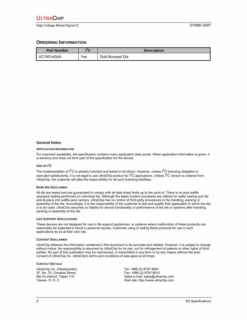
ORDERING INFORMATION Part Number I2C Description
UC1601sGAA Yes Gold Bumped Die
General Notes APPLICATION INFORMATION For improved readability, the specification contains many application data points. When application information is given, it is advisory and does not form part of the specification for the device.
USE OF I2C
The implementation of I2C is already included and tested in all silicon. However, unless I2C licensing obligation is executed satisfactorily, it is not legal to use UltraChip product for I2C applications. Unless I2C version is ordered from UltraChip, the customer will take the responsibility for all such licensing liabilities.
BARE DIE DISCLAIMER All die are tested and are guaranteed to comply with all data sheet limits up to the point of. There is no post waffle saw/pack testing performed on individual die. Although the latest modern processes are utilized for wafer sawing and die pick-&-place into waffle pack carriers, UltraChip has no control of third party procedures in the handling, packing or assembly of the die. Accordingly, it is the responsibility of the customer to test and qualify their application in which the die is to be used. UltraChip assumes no liability for device functionality or performance of the die or systems after handling, packing or assembly of the die.
LIFE SUPPORT APPLICATIONS These devices are not designed for use in life support appliances, or systems where malfunction of these products can reasonably be expected to result in personal injuries. Customer using or selling these products for use in such applications do so at their own risk.
CONTENT DISCLAIMER UltraChip believes the information contained in this document to be accurate and reliable. However, it is subject to change without notice. No responsibility is assumed by UltraChip for its use, nor for infringement of patents or other rights of third parties. No part of this publication may be reproduced, or transmitted in any form or by any means without the prior consent of UltraChip Inc. UltraChip's terms and conditions of sale apply at all times.
CONTACT DETAILS UltraChip Inc. (Headquarter) 2F, No. 70, Chowtze Street, Nei Hu District, Taipei 114, Taiwan, R. O. C.
Tel: +886 (2) 8797-8947 Fax: +886 (2) 8797-8910 Sales e-mail: [email protected] Web site: http://www.ultrachip.com
UC1601S 65x132 STN Controller-Drivers
Revision A_0.6 3
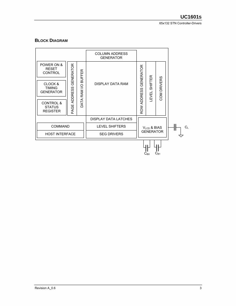
BLOCK DIAGRAM
DISPLAY DATA RAM
COLUMN ADDRESS GENERATOR
DISPLAY DATA LATCHES
LEVEL SHIFTERS
SEG DRIVERS
DA
TA R
AM
I/O
BU
FFE
R
PA
GE
AD
DR
ES
S G
EN
ER
ATO
R
RO
W A
DD
RE
SS
GE
NE
RA
TOR
LEV
EL
SH
IFTE
R
CO
M D
RIV
ER
S
VLCD & BIAS GENERATOR
HOST INTERFACE
COMMAND
CONTROL & STATUS
REGISTER
CLOCK & TIMING
GENERATOR
POWER ON & RESET
CONTROL
CB1CB0
CL
ULTRACHIP
High-Voltage Mixed-Signal IC ©1999~2007
4 ES Specifications
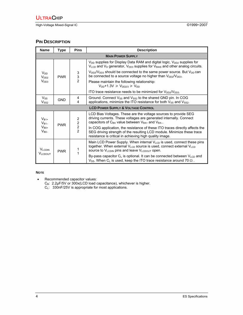
PIN DESCRIPTION Name Type Pins Description
MAIN POWER SUPPLY
VDD VDD2 VDD3
PWR 3 3 2
VDD supplies for Display Data RAM and digital logic, VDD2 supplies for VLCD and VD generator, VDD3 supplies for VBIAS and other analog circuits. VDD2/VDD3 should be connected to the same power source. But VDD can be connected to a source voltage no higher than VDD2/VDD3. Please maintain the following relationship:
VDD+1.3V VDD2/3 VDD ITO trace resistance needs to be minimized for VDD2/VDD3.
VSS VSS2
GND 4 4
Ground. Connect VSS and VSS2 to the shared GND pin. In COG applications, minimize the ITO resistance for both VSS and VSS2.
LCD POWER SUPPLY & VOLTAGE CONTROL
VB1+ VB1– VB0+ VB0–
PWR
2 2 2 2
LCD Bias Voltages. These are the voltage sources to provide SEG driving currents. These voltages are generated internally. Connect capacitors of CBX value between VBX+ and VBX–. In COG application, the resistance of these ITO traces directly affects the SEG driving strength of the resulting LCD module. Minimize these trace resistance is critical in achieving high quality image.
VLCDIN VLCDOUT PWR 1
1
Main LCD Power Supply. When internal VLCD is used, connect these pins together. When external VLCD source is used, connect external VLCD source to VLCDIN pins and leave VLCDOUT open. By-pass capacitor CL is optional. It can be connected between VLCD and VSS. When CL is used, keep the ITO trace resistance around 70 Ω .
NOTE
• Recommended capacitor values: CB: 2.2µF/5V or 300x(LCD load capacitance), whichever is higher. CL: 330nF/25V is appropriate for most applications.
UC1601S 65x132 STN Controller-Drivers
Revision A_0.6 5
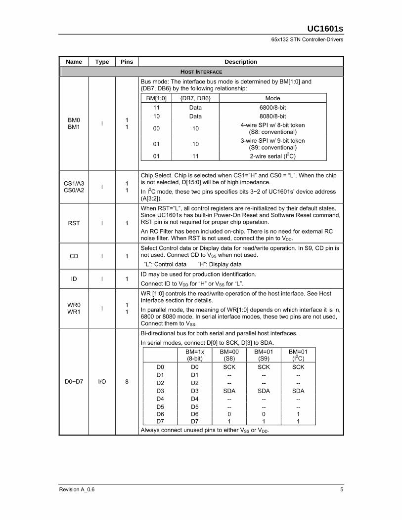
Name Type Pins Description HOST INTERFACE
BM0 BM1 I 1
1
Bus mode: The interface bus mode is determined by BM[1:0] and DB7, DB6 by the following relationship:
BM[1:0] DB7, DB6 Mode 11 Data 6800/8-bit 10 Data 8080/8-bit
00 10 4-wire SPI w/ 8-bit token (S8: conventional)
01 10 3-wire SPI w/ 9-bit token (S9: conventional)
01 11 2-wire serial (I2C)
CS1/A3 CS0/A2 I 1
1
Chip Select. Chip is selected when CS1=”H” and CS0 = “L”. When the chip is not selected, D[15:0] will be of high impedance. In I2C mode, these two pins specifies bits 3~2 of UC1601s’ device address (A[3:2]).
RST I 1
When RST=”L”, all control registers are re-initialized by their default states. Since UC1601s has built-in Power-On Reset and Software Reset command, RST pin is not required for proper chip operation. An RC Filter has been included on-chip. There is no need for external RC noise filter. When RST is not used, connect the pin to VDD.
CD I 1 Select Control data or Display data for read/write operation. In S9, CD pin is not used. Connect CD to VSS when not used. ”L”: Control data ”H”: Display data
ID I 1 ID may be used for production identification. Connect ID to VDD for “H” or VSS for “L”.
WR0 WR1 I 1
1
WR [1:0] controls the read/write operation of the host interface. See Host Interface section for details. In parallel mode, the meaning of WR[1:0] depends on which interface it is in, 6800 or 8080 mode. In serial interface modes, these two pins are not used, Connect them to VSS.
D0~D7 I/O 8
Bi-directional bus for both serial and parallel host interfaces. In serial modes, connect D[0] to SCK, D[3] to SDA.
BM=1x (8-bit)
BM=00 (S8)
BM=01 (S9)
BM=01 (I2C)
D0 D0 SCK SCK SCK D1 D1 -- -- -- D2 D2 -- -- -- D3 D3 SDA SDA SDA D4 D4 -- -- -- D5 D5 -- -- -- D6 D6 0 0 1 D7 D7 1 1 1
Always connect unused pins to either VSS or VDD.
ULTRACHIP
High-Voltage Mixed-Signal IC ©1999~2007
6 ES Specifications
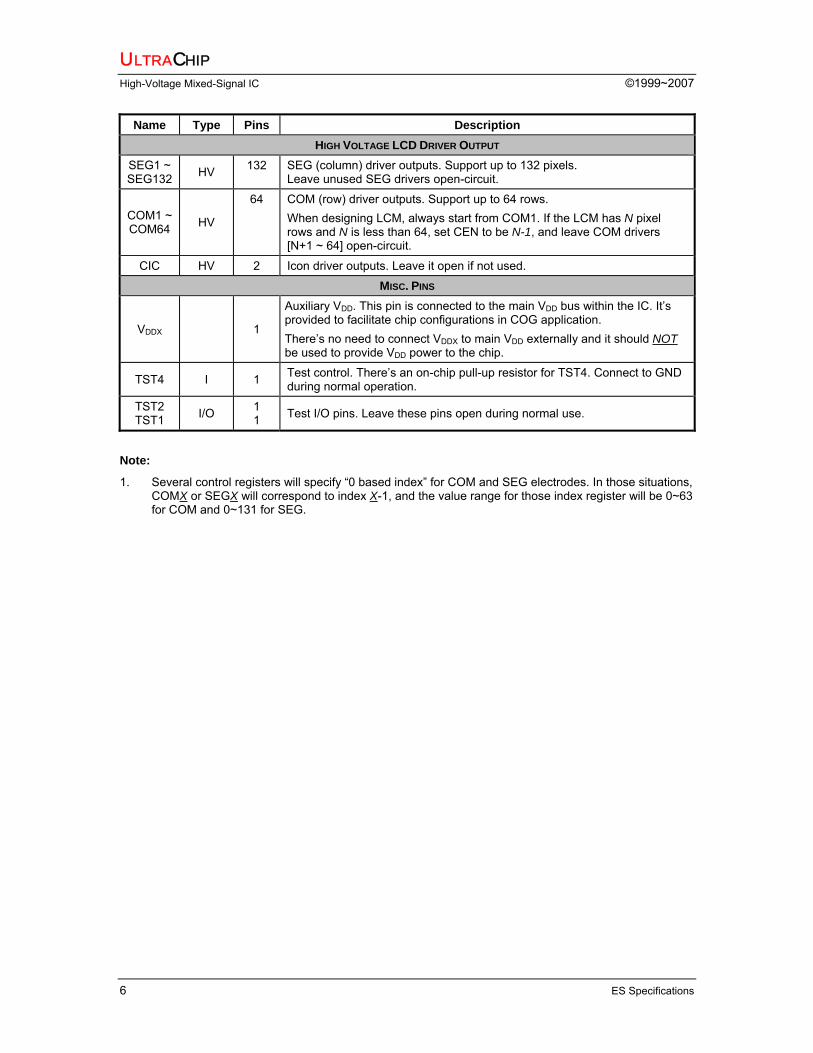
Name Type Pins Description HIGH VOLTAGE LCD DRIVER OUTPUT
SEG1 ~ SEG132 HV 132 SEG (column) driver outputs. Support up to 132 pixels.
Leave unused SEG drivers open-circuit.
COM1 ~ COM64 HV
64 COM (row) driver outputs. Support up to 64 rows. When designing LCM, always start from COM1. If the LCM has N pixel rows and N is less than 64, set CEN to be N-1, and leave COM drivers [N+1 ~ 64] open-circuit.
CIC HV 2 Icon driver outputs. Leave it open if not used.
MISC. PINS
VDDX 1
Auxiliary VDD. This pin is connected to the main VDD bus within the IC. It’s provided to facilitate chip configurations in COG application. There’s no need to connect VDDX to main VDD externally and it should NOT be used to provide VDD power to the chip.
TST4 I 1 Test control. There’s an on-chip pull-up resistor for TST4. Connect to GND during normal operation.
TST2 TST1 I/O 1
1 Test I/O pins. Leave these pins open during normal use.
Note:
1. Several control registers will specify “0 based index” for COM and SEG electrodes. In those situations, COMX or SEGX will correspond to index X-1, and the value range for those index register will be 0~63 for COM and 0~131 for SEG.
UC1601S 65x132 STN Controller-Drivers
Revision A_0.6 7
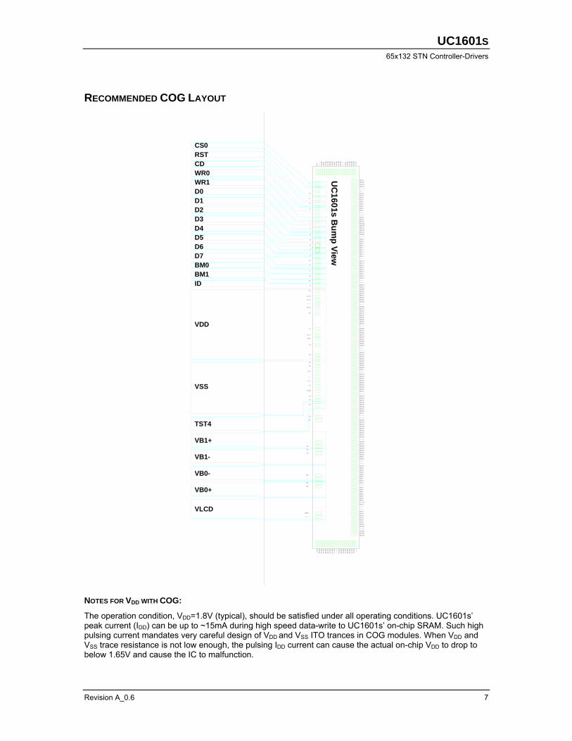
RECOMMENDED COG LAYOUT
UC
1601s Bum
p View
CS0RSTCDWR0WR1D0D1D2D3D4D5D6D7BM0BM1ID
VDD
VSS
TST4
VB1+
VB1-
VB0-
VB0+
VLCD
NOTES FOR VDD WITH COG:
The operation condition, VDD=1.8V (typical), should be satisfied under all operating conditions. UC1601s’ peak current (IDD) can be up to ~15mA during high speed data-write to UC1601s’ on-chip SRAM. Such high pulsing current mandates very careful design of VDD and VSS ITO trances in COG modules. When VDD and VSS trace resistance is not low enough, the pulsing IDD current can cause the actual on-chip VDD to drop to below 1.65V and cause the IC to malfunction.
ULTRACHIP
High-Voltage Mixed-Signal IC ©1999~2007
8 ES Specifications
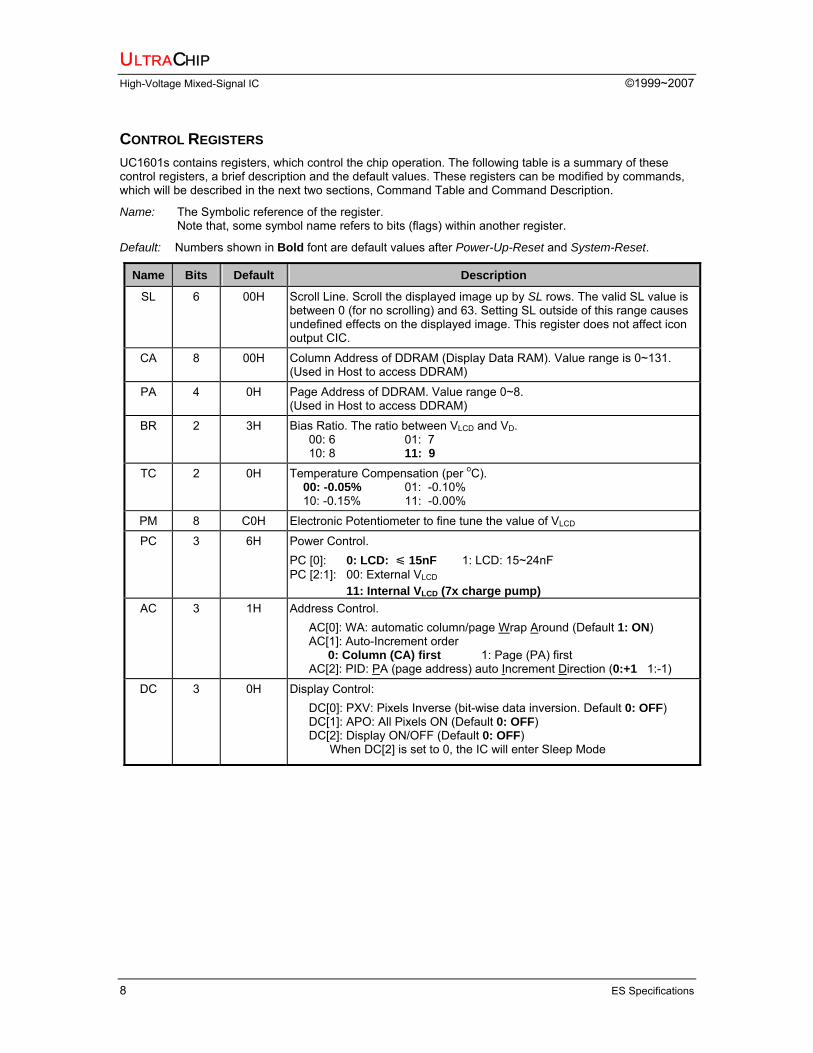
CONTROL REGISTERS UC1601s contains registers, which control the chip operation. The following table is a summary of these control registers, a brief description and the default values. These registers can be modified by commands, which will be described in the next two sections, Command Table and Command Description.
Name: The Symbolic reference of the register. Note that, some symbol name refers to bits (flags) within another register.
Default: Numbers shown in Bold font are default values after Power-Up-Reset and System-Reset.
Name Bits Default Description
SL 6 00H Scroll Line. Scroll the displayed image up by SL rows. The valid SL value is between 0 (for no scrolling) and 63. Setting SL outside of this range causes undefined effects on the displayed image. This register does not affect icon output CIC.
CA 8 00H Column Address of DDRAM (Display Data RAM). Value range is 0~131. (Used in Host to access DDRAM)
PA 4 0H Page Address of DDRAM. Value range 0~8. (Used in Host to access DDRAM)
BR 2 3H Bias Ratio. The ratio between VLCD and VD. 00: 6 01: 7 10: 8 11: 9
TC 2 0H Temperature Compensation (per oC). 00: -0.05% 01: -0.10% 10: -0.15% 11: -0.00%
PM 8 C0H Electronic Potentiometer to fine tune the value of VLCD
PC 3 6H Power Control. PC [0]: 0: LCD: 15nF 1: LCD: 15~24nF PC [2:1]: 00: External VLCD 11: Internal VLCD (7x charge pump)
AC 3 1H Address Control. AC[0]: WA: automatic column/page Wrap Around (Default 1: ON) AC[1]: Auto-Increment order 0: Column (CA) first 1: Page (PA) first AC[2]: PID: PA (page address) auto Increment Direction (0:+1 1:-1)
DC 3 0H Display Control: DC[0]: PXV: Pixels Inverse (bit-wise data inversion. Default 0: OFF) DC[1]: APO: All Pixels ON (Default 0: OFF) DC[2]: Display ON/OFF (Default 0: OFF) When DC[2] is set to 0, the IC will enter Sleep Mode
UC1601S 65x132 STN Controller-Drivers
Revision A_0.6 9
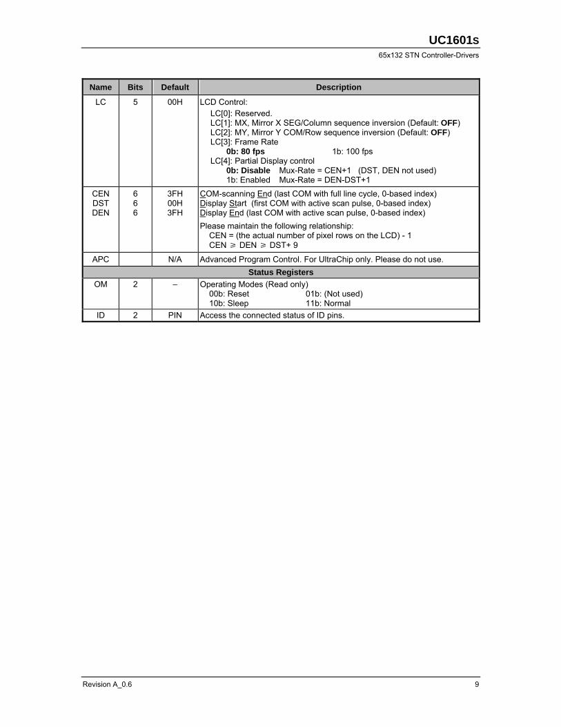
Name Bits Default Description
LC 5 00H LCD Control: LC[0]: Reserved. LC[1]: MX, Mirror X SEG/Column sequence inversion (Default: OFF) LC[2]: MY, Mirror Y COM/Row sequence inversion (Default: OFF) LC[3]: Frame Rate 0b: 80 fps 1b: 100 fps LC[4]: Partial Display control 0b: Disable Mux-Rate = CEN+1 (DST, DEN not used) 1b: Enabled Mux-Rate = DEN-DST+1
CEN DST DEN
6 6 6
3FH 00H 3FH
COM-scanning End (last COM with full line cycle, 0-based index) Display Start (first COM with active scan pulse, 0-based index) Display End (last COM with active scan pulse, 0-based index) Please maintain the following relationship: CEN = (the actual number of pixel rows on the LCD) - 1 CEN DEN DST+ 9
APC N/A Advanced Program Control. For UltraChip only. Please do not use. Status Registers
OM 2 – Operating Modes (Read only) 00b: Reset 01b: (Not used) 10b: Sleep 11b: Normal
ID 2 PIN Access the connected status of ID pins.
ULTRACHIP
High-Voltage Mixed-Signal IC ©1999~2007
10 ES Specifications
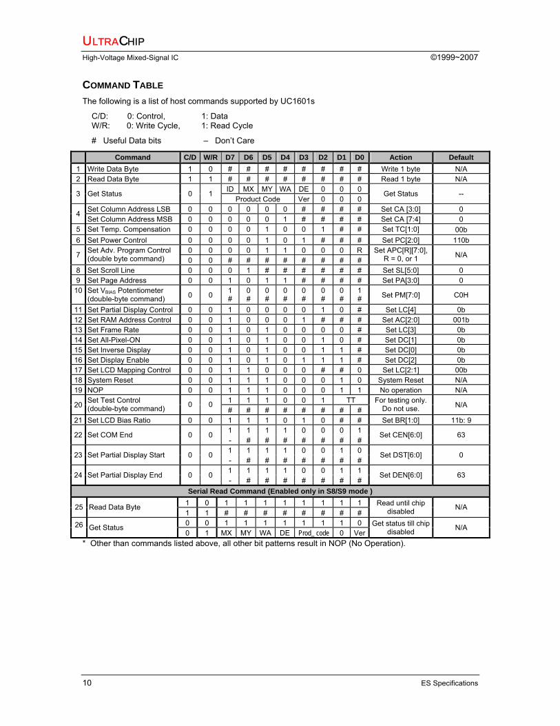
COMMAND TABLE The following is a list of host commands supported by UC1601s
C/D: 0: Control, 1: Data W/R: 0: Write Cycle, 1: Read Cycle
# Useful Data bits – Don’t Care
Command C/D W/R D7 D6 D5 D4 D3 D2 D1 D0 Action Default 1 Write Data Byte 1 0 # # # # # # # # Write 1 byte N/A 2 Read Data Byte 1 1 # # # # # # # # Read 1 byte N/A
ID MX MY WA DE 0 0 03 Get Status 0 1 Product Code Ver 0 0 0
Get Status --
Set Column Address LSB 0 0 0 0 0 0 # # # # Set CA [3:0] 0 4 Set Column Address MSB 0 0 0 0 0 1 # # # # Set CA [7:4] 0
5 Set Temp. Compensation 0 0 0 0 1 0 0 1 # # Set TC[1:0] 00b 6 Set Power Control 0 0 0 0 1 0 1 # # # Set PC[2:0] 110b
0 0 0 0 1 1 0 0 0 R7 Set Adv. Program Control (double byte command) 0 0 # # # # # # # #
Set APC[R][7:0], R = 0, or 1 N/A
8 Set Scroll Line 0 0 0 1 # # # # # # Set SL[5:0] 0 9 Set Page Address 0 0 1 0 1 1 # # # # Set PA[3:0] 0
10
Set VBIAS Potentiometer (double-byte command) 0 0 1
#0#
0#
0#
0#
0#
0#
1# Set PM[7:0] C0H
11 Set Partial Display Control 0 0 1 0 0 0 0 1 0 # Set LC[4] 0b 12 Set RAM Address Control 0 0 1 0 0 0 1 # # # Set AC[2:0] 001b 13 Set Frame Rate 0 0 1 0 1 0 0 0 0 # Set LC[3] 0b 14 Set All-Pixel-ON 0 0 1 0 1 0 0 1 0 # Set DC[1] 0b 15 Set Inverse Display 0 0 1 0 1 0 0 1 1 # Set DC[0] 0b 16 Set Display Enable 0 0 1 0 1 0 1 1 1 # Set DC[2] 0b 17 Set LCD Mapping Control 0 0 1 1 0 0 0 # # 0 Set LC[2:1] 00b 18 System Reset 0 0 1 1 1 0 0 0 1 0 System Reset N/A 19 NOP 0 0 1 1 1 0 0 0 1 1 No operation N/A
1 1 1 0 0 1 TT 20 Set Test Control (double-byte command) 0 0
# # # # # # # #For testing only.
Do not use. N/A
21 Set LCD Bias Ratio 0 0 1 1 1 0 1 0 # # Set BR[1:0] 11b: 9 1 1 1 1 0 0 0 122 Set COM End 0 0 - # # # # # # #
Set CEN[6:0] 63
1 1 1 1 0 0 1 023 Set Partial Display Start 0 0 - # # # # # # #
Set DST[6:0] 0
1 1 1 1 0 0 1 124 Set Partial Display End 0 0 - # # # # # # #
Set DEN[6:0] 63
Serial Read Command (Enabled only in S8/S9 mode ) 1 0 1 1 1 1 1 1 1 125 Read Data Byte 1 1 # # # # # # # #
Read until chip disabled N/A
0 0 1 1 1 1 1 1 1 026 Get Status 0 1 MX MY WA DE Prod_ code 0 Ver
Get status till chip disabled N/A
* Other than commands listed above, all other bit patterns result in NOP (No Operation).
UC1601S 65x132 STN Controller-Drivers
Revision A_0.6 11
COMMAND DESCRIPTION
1. Write Data Byte to Memory
Action C/D W/R D7 D6 D5 D4 D3 D2 D1 D0 Write data 1 0 8-bit data write to SRAM
2. Read Data Byte from Memory
Action C/D W/R D7 D6 D5 D4 D3 D2 D1 D0 Read data 1 1 8-bit data read from SRAM
Write/Read Data Byte (Command 1,2) access Display Data RAM based on Page Address (PA) register and Column Address (CA) register. To minimize bus interface cycles, PA and CA will increase or decrease automatically after each bus cycle, depending on the setting of Access Control (AC) registers. PA and CA can also be programmed directly by issuing Set Page Address and Set Column Address commands.
If Wrap-Around (WA) is OFF (AC[0] = 0), CA will stop increasing after reaching the end of the page, and system programmers need to set the values of PA and CA explicitly. If WA is ON (AC[0]=1), when CA reaches the end of the page, CA will be reset to 0 and PA will increase or decrease by 1, depending on the setting of Page Increment Direction (PID, AC[2]). When PA reaches the boundary of RAM, PA will be wrapped around to the other end of RAM and continue. (See command 30, Window Programming, for more details)
3. Get Status
Action C/D W/R D7 D6 D5 D4 D3 D2 D1 D0 0 1 ID MX MY WA DE 0 0 0
Get Status 0 1 Product Code Ver 0 0 0
Status1 definitions: ID: Provide access to ID pins connection status. MX: Status of register LC[1], mirror X. MY: Status of register LC[2], mirror Y. WA: Status of register AC[0]. Automatic column/row wrap around. DE: Display Enable flag. DE=1 when display is enabled.
Status2 definitions: Product Code: production identification. Default: 0110b. Ver: IC Version, 0~ 1.
4. Set Column Address
Action C/D W/R D7 D6 D5 D4 D3 D2 D1 D0 Set Column Address LSB CA[3:0] 0 0 0 0 0 0 CA3 CA2 CA1 CA0 Set Column Address MSB CA[7:4] 0 0 0 0 0 1 CA7 CA6 CA5 CA4
Set the SRAM column address before Write/Read memory from host interface.
CA value range: 0~131
ULTRACHIP
High-Voltage Mixed-Signal IC ©1999~2007
12 ES Specifications
5. Set Temperature Compensation
Action C/D W/R D7 D6 D5 D4 D3 D2 D1 D0 Set Temperature Comp. TC[1:0] 0 0 0 0 1 0 0 1 TC1 TC0
Set VBIAS temperature compensation coefficient (%-per-degree-C)
Temperature compensation curve definition:
00b= -0.05%/ oC 01b= -0.10%/ oC 10b= -0.15%/ oC 11b= -0.00%/oC
6. Set Power Control
Action C/D W/R D7 D6 D5 D4 D3 D2 D1 D0 Set Power Control PC[2:0] 0 0 0 0 1 0 1 PC2 PC1 PC0
Set PC[0] according to the capacitance loading of LCD panel. Panel loading definition: 0b : 15nF 1b : 15~24nF
Set PC[2:1] to program the build-in charge pump stages. 00b = External VLCD 11b = Internal VLCD ( x7 )
7. Set Advanced Program Control
Action C/D W/R D7 D6 D5 D4 D3 D2 D1 D0 0 0 0 0 1 1 0 0 0 R Set Adv. Program Control
APC[R][7:0](Double byte command) 0 0 APC register parameter For UltraChip only. Please Do NOT use.
8. Set Scroll Line
Action C/D W/R D7 D6 D5 D4 D3 D2 D1 D0 Set Scroll Line SL[5:0] 0 0 0 1 SL5 SL4 SL3 SL2 SL1 SL0
Set the scroll line number.
Scroll line setting will scroll the displayed image up by SL rows. Icon output CIC will not be affected by Set Scroll Line command.
Image row 0 : Image row N-1 Image row N : : Image row 63
row 0 : : row 63
Image row N : : Image row 63 Image row 0 : Image row N-1
row 0 : : row 63
SL=0 SL=N
9. Set Page Address
Action C/D W/R D7 D6 D5 D4 D3 D2 D1 D0 Set Page Address 0 0 1 0 1 1 PA3 PA2 PA1 PA0
Set the SRAM page address before write/read memory from host interface. Each page of SRAM corresponds to 8 COM lines on LCD panel, except for the last page. The last page corresponds to the icon output CIC.
Possible value = 0~8.
UC1601S 65x132 STN Controller-Drivers
Revision A_0.6 13
10. Set VBIAS Potentiometer
Action C/D W/R D7 D6 D5 D4 D3 D2 D1 D0 0 0 1 0 0 0 0 0 0 1 Set VBIAS Potentiometer PM [7:0]
(Double byte command) 0 0 PM7 PM6 PM5 PM4 PM3 PM2 PM1 PM0 Program VBIAS Potentiometer (PM[7:0]). See section LCD Voltage Setting for more detail.
Effective range: 0 ~ 255
11. Set Partial Display Control
Action C/D W/R D7 D6 D5 D4 D3 D2 D1 D0 Set Partial Display Enable LC [4] 0 0 1 0 0 0 0 1 0 LC4
This command is used to enable partial display function.
LC[4] : 0b: Disable Partial Display, Mux-Rate = CEN+1 (DST, DEN not used.) 1b: Enable Partial Display, Mux-Rate = DEN-DST+1
12. Set RAM Address Control
Action C/D W/R D7 D6 D5 D4 D3 D2 D1 D0 Set AC [2:0] 0 0 1 0 0 0 1 AC2 AC1 AC0
Program registers AC[2:0] for RAM address control. It controls the auto-increment behavior of CA and PA.
AC[0] – WA, Automatic column/page wrap around. 0: CA or PA (depends on AC[1]= 0 or 1) will stop increasing after reaching boundary 1: CA or PA (depends on AC[1]= 0 or 1) will restart, and CA or PA will increase by one.
AC[1] – Auto-Increment order 0 : column (CA) increasing (+1) first until CA reach CA boundary, then PA will increase by (+/-1). 1 : page (PA) increasing (+/-1) first until PA reach PA boundary, then CA will increase by (+1).
AC[2] – PID, page address (PA) auto increment direction ( 0/1 = +/- 1 ) When WA=1 and CA reaches CA boundary, PID controls whether page address will be adjusted by +1 or -1.
13. Set Frame Rate
Action C/D W/R D7 D6 D5 D4 D3 D2 D1 D0 Set Frame Rate LC [3] 0 0 1 0 1 0 0 0 0 LC3
Program LC [3] for frame rate setting
0b: 80 fps 1b: 100 fps (fps: frame-per-second)
ULTRACHIP
High-Voltage Mixed-Signal IC ©1999~2007
14 ES Specifications
14. Set All Pixel ON
Action C/D W/R D7 D6 D5 D4 D3 D2 D1 D0 Set All Pixel ON DC [1] 0 0 1 0 1 0 0 1 0 DC1
Set DC[1] to force all SEG drivers to output ON signals. This function has no effect on the existing data stored in display RAM.
15. Set Inverse Display
Action C/D W/R D7 D6 D5 D4 D3 D2 D1 D0 Set Inverse Display DC [0] 0 0 1 0 1 0 0 1 1 DC0
Set DC[0] to force all SEG drivers to output the inverse of the data (bit-wise) stored in display RAM. This function has no effect on the existing data stored in display RAM.
16. Set Display Enable
Action C/D W/R D7 D6 D5 D4 D3 D2 D1 D0 Set Display Enable DC[2] 0 0 1 0 1 0 1 1 1 DC2
This command is for programming register DC[2]. When DC[2] is set to 1, UC1601s will first exit from sleep mode, restore the power and then turn on COM drivers and SEG drivers.
17. Set LCD Mapping Control
Action C/D W/R D7 D6 D5 D4 D3 D2 D1 D0 Set LCD Control LC[2:1] 0 0 1 1 0 0 0 MY MX 0
Set LC[2:1] for COM (row) mirror (MY), SEG (column) mirror (MX).
MY is implemented by reversing the mapping order between RAM and COM (row) electrodes. The data stored in RAM is not affected by MY command. MY will have immediate effect on the display image.
MX is implemented by selecting the CA or 50-CA as write/read (from host interface) display RAM column address so this function will only take effect after rewriting the RAM data.
18. System Reset
Action C/D W/R D7 D6 D5 D4 D3 D2 D1 D0 System Reset 0 0 1 1 1 0 0 0 1 0
This command will activate the system reset.
Control register values will be reset to their default values. Data store in RAM will not be affected.
19. NOP
Action C/D W/R D7 D6 D5 D4 D3 D2 D1 D0 No Operation 0 0 1 1 1 0 0 0 1 1
This command is used for “no operation”.
20. Set Test Control
Action C/D W/R D7 D6 D5 D4 D3 D2 D1 D0 0 0 1 1 1 0 0 1 TT Set TT
(Double byte command) 0 0 Testing parameter This command is used for UltraChip production testing. Please do NOT use.
UC1601S 65x132 STN Controller-Drivers
Revision A_0.6 15
21. Set LCD Bias Ratio
Action C/D W/R D7 D6 D5 D4 D3 D2 D1 D0 Set Bias Ratio BR [1:0] 0 0 1 1 1 0 1 0 BR1 BR0
Bias ratio definition: 00b= 6 01b= 7 10b= 8 11b= 9
22. Set COM End
Action C/D W/R D7 D6 D5 D4 D3 D2 D1 D0 0 0 1 1 1 1 0 0 0 1 Set CEN [6:0]
(Double-byte command) 0 0 - CEN register parameter
This command programs the ending COM electrode. CEN defines the number of used COM electrodes, and it should correspond to the number of pixel-rows in the LCD. When the LCD has less than 64 pixel rows, the LCM designer should set CEN to N-1 (where N is the number of pixel rows) and use COM1 through COM-N as COM driver electrodes.
ULTRACHIP
High-Voltage Mixed-Signal IC ©1999~2007
16 ES Specifications
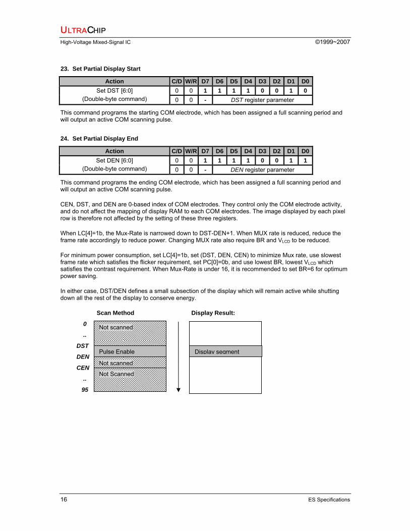
23. Set Partial Display Start
Action C/D W/R D7 D6 D5 D4 D3 D2 D1 D0 0 0 1 1 1 1 0 0 1 0 Set DST [6:0]
(Double-byte command) 0 0 - DST register parameter
This command programs the starting COM electrode, which has been assigned a full scanning period and will output an active COM scanning pulse.
24. Set Partial Display End
Action C/D W/R D7 D6 D5 D4 D3 D2 D1 D0 0 0 1 1 1 1 0 0 1 1 Set DEN [6:0]
(Double-byte command) 0 0 - DEN register parameter
This command programs the ending COM electrode, which has been assigned a full scanning period and will output an active COM scanning pulse.
CEN, DST, and DEN are 0-based index of COM electrodes. They control only the COM electrode activity, and do not affect the mapping of display RAM to each COM electrodes. The image displayed by each pixel row is therefore not affected by the setting of these three registers.
When LC[4]=1b, the Mux-Rate is narrowed down to DST-DEN+1. When MUX rate is reduced, reduce the frame rate accordingly to reduce power. Changing MUX rate also require BR and VLCD to be reduced.
For minimum power consumption, set LC[4]=1b, set (DST, DEN, CEN) to minimize Mux rate, use slowest frame rate which satisfies the flicker requirement, set PC[0]=0b, and use lowest BR, lowest VLCD which satisfies the contrast requirement. When Mux-Rate is under 16, it is recommended to set BR=6 for optimum power saving.
In either case, DST/DEN defines a small subsection of the display which will remain active while shutting down all the rest of the display to conserve energy.
Scan Method Display Result:
0
..
DST
DEN
CEN
..
95
Not scanned
Pulse Enable
Not scanned
Not Scanned
Display segment
UC1601S 65x132 STN Controller-Drivers
Revision A_0.6 17
Serial Read Command (Enable only in S8/S9 mode):
25. Read Data Byte from Memory
Action C/D W/R D7 D6 D5 D4 D3 D2 D1 D0 1 1 1 1 1 1 1 1
Read data 1 18-bit Data read from SRAM
26. Get Status
Action C/D W/R D7 D6 D5 D4 D3 D2 D1 D0 1 1 1 1 1 1 1 0
Get Status 0 1MX MY WA DE Prod_Code 0 Ver
ULTRACHIP
High-Voltage Mixed-Signal IC ©1999~2007
18 ES Specifications
LCD VOLTAGE SETTING
MULTIPLEX RATES
Multiplex Rate is completely software programmable in UC1601s via registers CEN, DST, DEN, and partial display control flags LC[4].
Combined with low power partial display mode and a low bias ratio of 6, UC1601s can support wide variety of display control options. For example, when a system goes into stand-by mode, a large portion of LCD screen can be turned off to conserve power.
BIAS RATIO SELECTION Bias Ratio (BR) is defined as the ratio between VLCD and VBIAS, i.e.
BR = VLCD /VBIAS,
where VBIAS = VB1+ – VB1– = VB0+ – VB0–.
The theoretical optimum Bias Ratio can be estimated by 1+Mux . BR of value 15~20% lower/higher than the optimum value calculated above will not cause significant visible change in image quality.
UC1601s supports four BR as listed below. BR can be selected by software program.
BR 0 1 2 3 Bias Ratio 6 7 8 9
Table 1: Bias Ratios
TEMPERATURE COMPENSATION Four different temperature compensation coefficients can be selected via software. The four coefficients are given below:
TC 0 1 2 3
% per oC –0.05 –0.10 –0.15 –0.00
Table 2: Temperature Compensation
VLCD GENERATION VLCD may be supplied either by internal charge pump or by external power supply. The source of VLCD is controlled by PC[2:1].
When VLCD is generated internally, the voltage level of VLCD is determined by three control registers: BR (Bias Ratio), PM (Potentiometer), and TC (Temperature Compensation), with the following relationship: %))25(1()( 0 TPMVLCD CTPMCCV ×−+××+=
where
CV0 and CPM are two constants, whose value depends on the setting of BR register, as illustrated in the table on the next page,
PM is the numerical value of PM register,
T is the ambient temperature in OC, and
CT is the temperature compensation coefficient as selected by TC register.
VLCD FINE TUNING Black-and-white STN LCD is sensitive to even a 1% mismatch between IC driving voltage and the VOP of LCD. However, it is difficult for LCD makers to guarantee such high precision matching of parts from different venders. It is therefore necessary to adjust VLCD to match the actual VOP of the LCD.
For the best result, software based approach for VLCD adjustment is the recommended method for VLCD fine-tuning. System designers should always consider the contrast fine tuning requirement before finalizing on the LEM design
LOAD DRIVING STRENGTH The power supply circuit of UC1601s is designed to handle LCD panels with loading up to ~24nF using 20-Ω/Sq ITO glass with VDD2/3 2.4V. For larger LCD panels, use lower resistance ITO glass packaging.
UC1601S 65x132 STN Controller-Drivers
Revision A_0.6 19
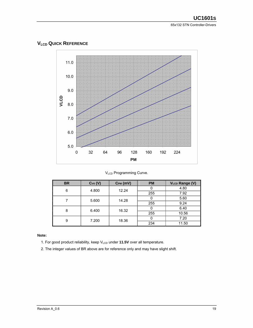
VLCD QUICK REFERENCE
5.0
6.0
7.0
8.0
9.0
10.0
11.0
0 32 64 96 128 160 192 224
PM
VLC
D
VLCD Programming Curve.
BR CV0 (V) CPM (mV) PM VLCD Range (V) 0 4.80 6 4.800 12.24
255 7.92 0 5.60 7 5.600 14.28
255 9.24 0 6.40 8 6.400 16.32
255 10.56 0 7.20 9 7.200 18.36
234 11.50
Note:
1. For good product reliability, keep VLCD under 11.5V over all temperature.
2. The integer values of BR above are for reference only and may have slight shift.
ULTRACHIP
High-Voltage Mixed-Signal IC ©1999~2007
20 ES Specifications
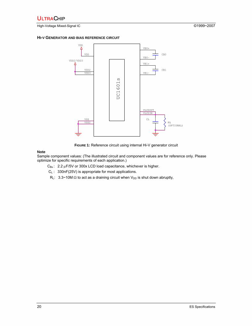
HI-V GENERATOR AND BIAS REFERENCE CIRCUIT VDD
VLCDIN
UC1601s
VB1+
VDD
VB1-VDD3
CL
CB0
VDD2/VDD3
VLCDOUT
CB1
VSS
VB0-
VSS2(OPTIONAL)RL
VB0+
VDD2
FIGURE 1: Reference circuit using internal Hi-V generator circuit
Note Sample component values: (The illustrated circuit and component values are for reference only. Please optimize for specific requirements of each application.) CBx : 2.2 µF/5V or 300x LCD load capacitance, whichever is higher. CL : 330nF(25V) is appropriate for most applications.
RL: 3.3~10M Ω to act as a draining circuit when VDD is shut down abruptly.
UC1601S 65x132 STN Controller-Drivers
Revision A_0.6 21
LCD DISPLAY CONTROLS
CLOCK & TIMING GENERATOR UC1601s contains a built-in system clock. All required components for the clock oscillator are built-in. No external parts are required.
Two different frame rates are provided for system design flexibility. The frame rate is controlled by register LC[3]. When Mux-Rate is above 34, Frame rate: 80 fps and 100 fps.
When Mux-Rate is lowered to 33, and 16, frame rate will be scaled down automatically by 2 and 4 times to reduce power consumption.
Choose lower frame rate for lower power, and choose higher frame rate to improve LCD contrast and minimize flicker.
DRIVER MODES COM and SEG drivers can be in either Idle mode or Active mode, controlled by Display Enable flag (DC[2]). When SEG and COM drivers are in idle mode, they will be connected together to ensure zero DC condition on the LCD.
DRIVER ARRANGEMENTS The naming conventions are: COMx, where x = 1~64, refers to the row driver for the x-th row of pixels on the LCD panel.
The mapping of COM(x) to LCD pixel rows is fixed and it is not affected by SL, CEN, DST, DEN, MX or MY settings.
DISPLAY CONTROLS There are three groups of display control flags in the control register DC: Driver Enable (DE), All-Pixel-ON (APO) and Inverse (PXV). DE has the overriding effect over PXV and APO.
DRIVER ENABLE (DE) Driver Enable is controlled by the value of DC[2] via Set Display Enable command. When DC[2] is set to OFF (logic “0”), both COM and SEG drivers will become idle and UC1601s will put itself into Sleep Mode to conserve power.
When DC[2] is set to ON, the DE flag will become “1”,and UC1601s will first exit from Sleep Mode, restore the power (VLCD, VD etc.) and then turn on COM and SEG drivers.
ALL PIXELS ON (APO)
When set, this flag will force all SEG drivers to output ON signals, disregarding the data stored in the display buffer.
This flag has no effect when Display Enable is OFF and it has no effect on data stored in RAM.
INVERSE (PXV)
When this flag set to ON, SEG drivers will output the inverse of the value it received from the display buffer RAM (bit-wise inversion). This flag has no impact on data stored in RAM.
PARTIAL DISPLAY
UC1601s provides flexible control of Mux Rate and active display area. Please refer to commands Set COM End, Set Partial Display Start, and Set Partial Display End for more detail.
ULTRACHIP
High-Voltage Mixed-Signal IC ©1999~2007
22 ES Specifications
ITO LAYOUT AND LC SELECTION Since COM scanning pulses of UC1601s can be as short as 153µS, it is critical to control the RC delay of COM and SEG signal to minimize crosstalk and maintain good mass production consistency.
COM TRACES Excessive COM scanning pulse RC decay can cause fluctuation of contrast and increase COM direction crosstalk.
Please limit the worst case of COM signals RC delay (RCMAX) as calculated below
(RROW / 2.7 + RCOM) x CROW < 9.23µS
where
CROW: LCD loading capacitance of one row of pixels. It can be calculated by CLCD/Mux-Rate, where CLCD is the LCD panel capacitance.
RROW: ITO resistance over one row of pixels within the active area
RCOM: COM routing resistance from IC to the active area + COM driver output impedance.
In addition, please limit the min-max spread of RC decay to be:
| RCMAX – RCMIN | < 2.76µS
so that the COM distortions on the top of the screen to the bottom of the screen are uniform.
(Use worst case values for all calculations)
SEG TRACES Excessive SEG signal RC decay can cause image dependent changes of medium gray shades and sharply increase the crosstalk of SEG direction.
For good image quality, please minimize SEG ITO trace resistance and limit the worst case of SEG signal RC delay as calculated below.
(RCOL / 2.7 + RSEG) x CCOL < 6.30µS
where
CCOL: LCD loading capacitance of one pixel column. It can be calculated by CLCD / (# of column), where CLCD is the LCD panel capacitance.
RCOL: ITO resistance over one column of pixels within the active area
RSEG: SEG routing resistance from IC to the active area + SEG driver output impedance.
(Use worst case values for all calculations)
SELECTING LIQUID CRYSTAL The selection of LC material is crucial to achieve the optimum image quality of finished LCM.
When (V90-V10)/V10 is too large, image contrast will deteriorate, and images will look murky and dull.
When (V90-V10)/V10 is too small, image contrast will become too strong, and crosstalk will increase.
For the best result, it is recommended the LC material has the following characteristics:
(V90-V10)/V10 = (VON-VOFF)/VOFF x 0.72~0.80
where V90 and V10 are the LC characteristics, and VON and VOFF are the ON and OFF VRMS voltage produced by LCD driver IC at the specific Mux-rate.
Two examples are provided below:
Duty Bias VON/VOFF -1 x0.80 x0.721/65 1/9 10.6% 9.6% 7.5%1/65 1/8 10.5% 9.5% 7.4%
UC1601S 65x132 STN Controller-Drivers
Revision A_0.6 23
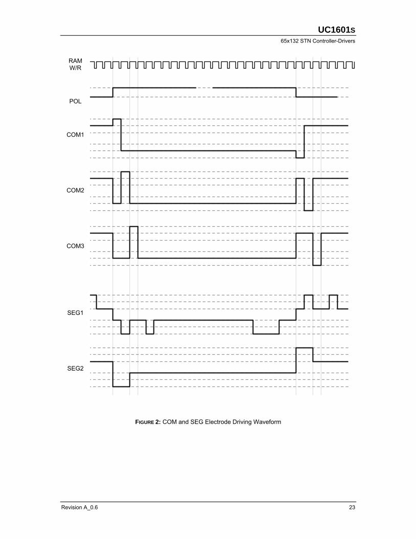
FIGURE 2: COM and SEG Electrode Driving Waveform
RAM W/R
POL
COM1
COM2
COM3
SEG1
SEG2
ULTRACHIP
High-Voltage Mixed-Signal IC ©1999~2007
24 ES Specifications
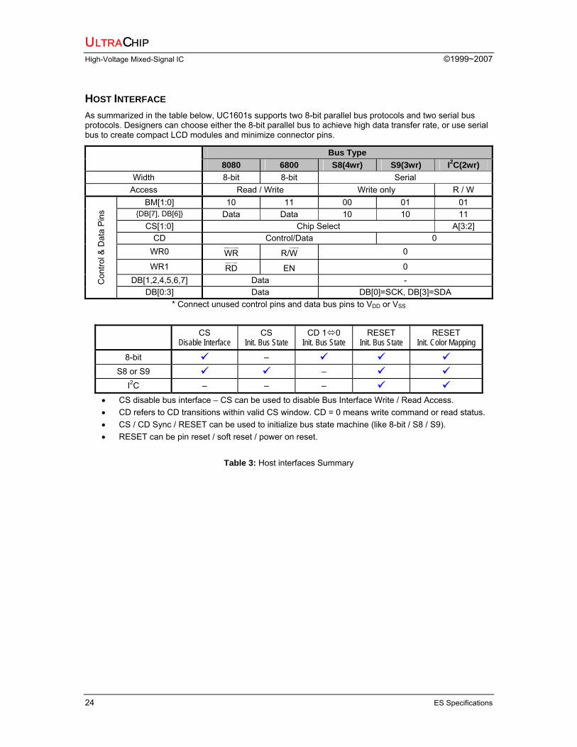
HOST INTERFACE As summarized in the table below, UC1601s supports two 8-bit parallel bus protocols and two serial bus protocols. Designers can choose either the 8-bit parallel bus to achieve high data transfer rate, or use serial bus to create compact LCD modules and minimize connector pins.
Bus Type 8080 6800 S8(4wr) S9(3wr) I2C(2wr)
Width 8-bit 8-bit Serial Access Read / Write Write only R / W
BM[1:0] 10 11 00 01 01 DB[7], DB[6] Data Data 10 10 11
CS[1:0] Chip Select A[3:2] CD Control/Data 0
WR0 ___ __
WR _ _ R/W 0
WR1 ___ __ RD EN 0
DB[1,2,4,5,6,7] Data - Con
trol &
Dat
a P
ins
DB[0:3] Data DB[0]=SCK, DB[3]=SDA * Connect unused control pins and data bus pins to VDD or VSS
CS Disable Interface
CS Init. Bus State
CD 1 0 Init. Bus State
RESET Init. Bus State
RESET Init. Color Mapping
8-bit – S8 or S9 –
I2C – – – • CS disable bus interface – CS can be used to disable Bus Interface Write / Read Access. • CD refers to CD transitions within valid CS window. CD = 0 means write command or read status. • CS / CD Sync / RESET can be used to initialize bus state machine (like 8-bit / S8 / S9). • RESET can be pin reset / soft reset / power on reset.
Table 3: Host interfaces Summary
UC1601S 65x132 STN Controller-Drivers
Revision A_0.6 25
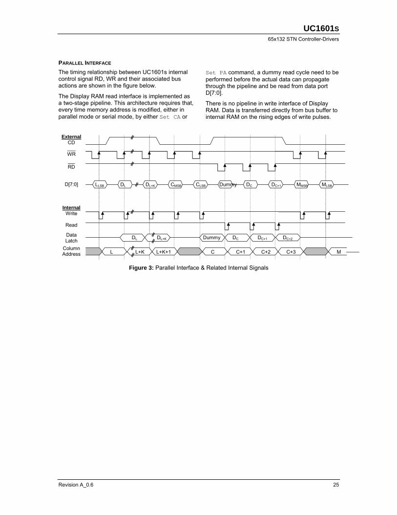
PARALLEL INTERFACE The timing relationship between UC1601s internal control signal RD, WR and their associated bus actions are shown in the figure below.
The Display RAM read interface is implemented as a two-stage pipeline. This architecture requires that, every time memory address is modified, either in parallel mode or serial mode, by either Set CA or
Set PA command, a dummy read cycle need to be performed before the actual data can propagate through the pipeline and be read from data port D[7:0].
There is no pipeline in write interface of Display RAM. Data is transferred directly from bus buffer to internal RAM on the rising edges of write pulses.
LLSB DL DL+K CMSB CLSB Dummy DC DC+1 MMSB MLSB
L L+K L+K+1 C C+1 C+2 C+3 M
DL DL+K Dummy DC DC+1 DC+2
External CD ___ WR __ RD
D[7:0]
Internal Write
Read
Data Latch
Column Address
Figure 3: Parallel Interface & Related Internal Signals
ULTRACHIP
High-Voltage Mixed-Signal IC ©1999~2007
26 ES Specifications
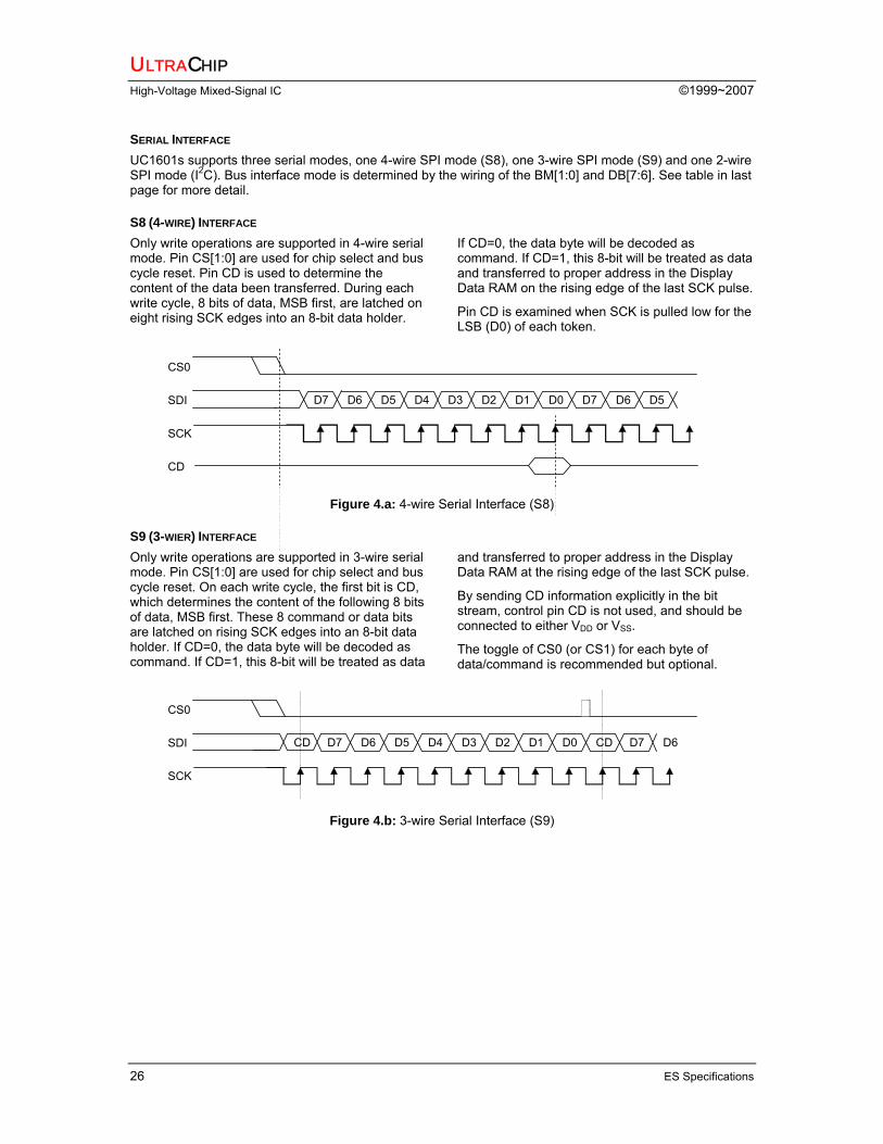
SERIAL INTERFACE UC1601s supports three serial modes, one 4-wire SPI mode (S8), one 3-wire SPI mode (S9) and one 2-wire SPI mode (I2C). Bus interface mode is determined by the wiring of the BM[1:0] and DB[7:6]. See table in last page for more detail.
S8 (4-WIRE) INTERFACE Only write operations are supported in 4-wire serial mode. Pin CS[1:0] are used for chip select and bus cycle reset. Pin CD is used to determine the content of the data been transferred. During each write cycle, 8 bits of data, MSB first, are latched on eight rising SCK edges into an 8-bit data holder.
If CD=0, the data byte will be decoded as command. If CD=1, this 8-bit will be treated as data and transferred to proper address in the Display Data RAM on the rising edge of the last SCK pulse.
Pin CD is examined when SCK is pulled low for the LSB (D0) of each token.
CS0
SDI
SCK
CD
D7 D6 D5 D4 D3 D2 D1 D0 D7 D6 D5
Figure 4.a: 4-wire Serial Interface (S8)
S9 (3-WIER) INTERFACE Only write operations are supported in 3-wire serial mode. Pin CS[1:0] are used for chip select and bus cycle reset. On each write cycle, the first bit is CD, which determines the content of the following 8 bits of data, MSB first. These 8 command or data bits are latched on rising SCK edges into an 8-bit data holder. If CD=0, the data byte will be decoded as command. If CD=1, this 8-bit will be treated as data
and transferred to proper address in the Display Data RAM at the rising edge of the last SCK pulse.
By sending CD information explicitly in the bit stream, control pin CD is not used, and should be connected to either VDD or VSS.
The toggle of CS0 (or CS1) for each byte of data/command is recommended but optional.
CS0
SDI
SCK
CD D7 D6 D5 D4 D3 D2 D1 D0 CD D7 D6
Figure 4.b: 3-wire Serial Interface (S9)
UC1601S 65x132 STN Controller-Drivers
Revision A_0.6 27
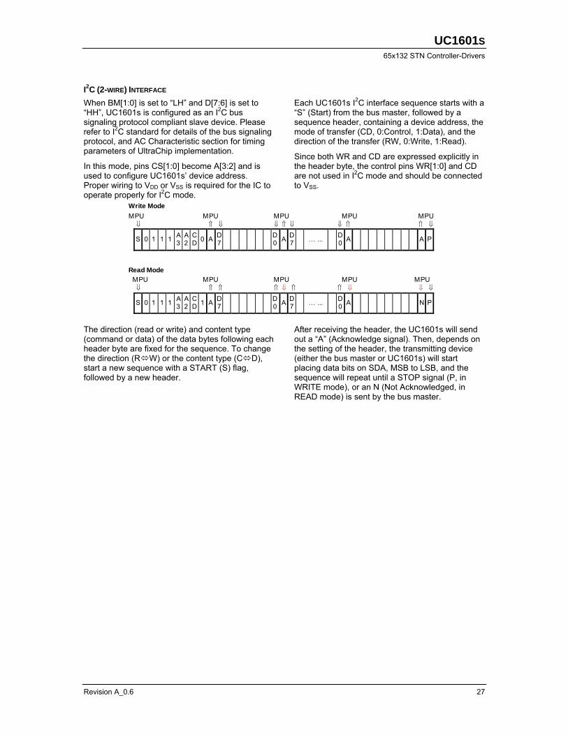
I2C (2-WIRE) INTERFACE
When BM[1:0] is set to “LH” and D[7:6] is set to “HH”, UC1601s is configured as an I2C bus signaling protocol compliant slave device. Please refer to I2C standard for details of the bus signaling protocol, and AC Characteristic section for timing parameters of UltraChip implementation.
In this mode, pins CS[1:0] become A[3:2] and is used to configure UC1601s’ device address. Proper wiring to VDD or VSS is required for the IC to operate properly for I2C mode.
Each UC1601s I2C interface sequence starts with a “S” (Start) from the bus master, followed by a sequence header, containing a device address, the mode of transfer (CD, 0:Control, 1:Data), and the direction of the transfer (RW, 0:Write, 1:Read).
Since both WR and CD are expressed explicitly in the header byte, the control pins WR[1:0] and CD are not used in I2C mode and should be connected to VSS.
Write Mode MPU MPU MPU MPU MPU ⇓ ⇑ ⇓ ⇓ ⇑ ⇓ ⇓ ⇑ ⇑ ⇓
S 0 1 1 1 A 3
A 2
C D 0 A D
7 D0 A D
7 … ... D0 A A P
Read Mode MPU MPU MPU MPU MPU ⇓ ⇑ ⇑ ⇑ ⇓ ⇑ ⇑ ⇓ ⇓ ⇓
S 0 1 1 1 A 3
A 2
C D 1 A D
7 D0 A D
7 … ... D0 A N P
The direction (read or write) and content type (command or data) of the data bytes following each header byte are fixed for the sequence. To change the direction (R W) or the content type (C D), start a new sequence with a START (S) flag, followed by a new header.
After receiving the header, the UC1601s will send out a “A” (Acknowledge signal). Then, depends on the setting of the header, the transmitting device (either the bus master or UC1601s) will start placing data bits on SDA, MSB to LSB, and the sequence will repeat until a STOP signal (P, in WRITE mode), or an N (Not Acknowledged, in READ mode) is sent by the bus master.
ULTRACHIP
High-Voltage Mixed-Signal IC ©1999~2007
28 ES Specifications
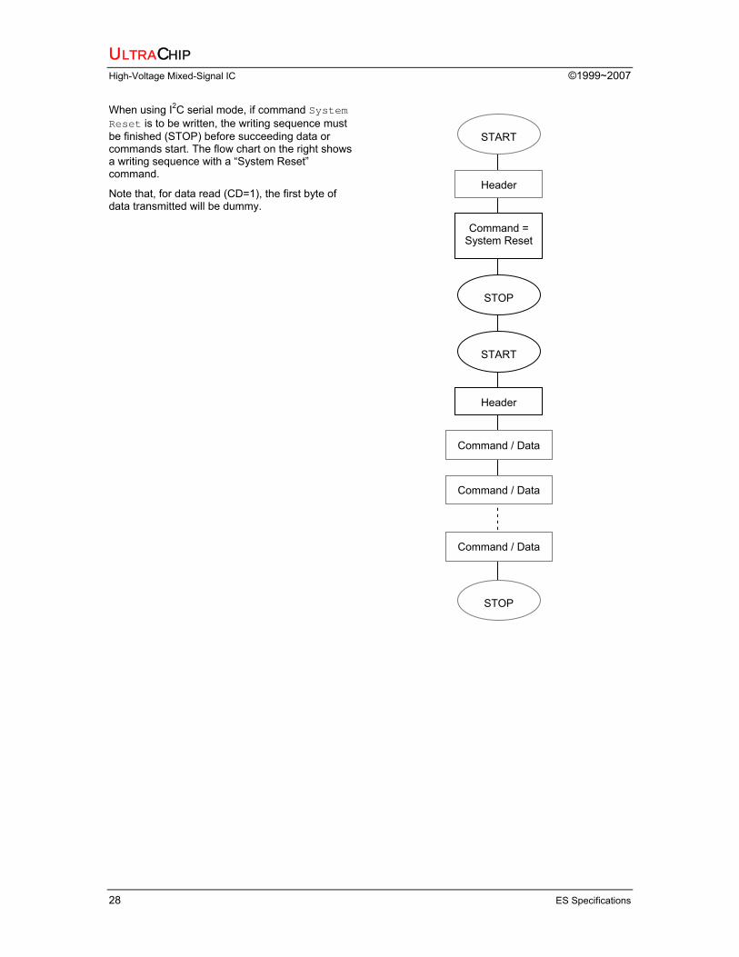
When using I2C serial mode, if command System Reset is to be written, the writing sequence must be finished (STOP) before succeeding data or commands start. The flow chart on the right shows a writing sequence with a “System Reset” command.
Note that, for data read (CD=1), the first byte of data transmitted will be dummy.
START
Header
STOP
START
Header
Command / Data
STOP
Command = System Reset
Command / Data
Command / Data
UC1601S 65x132 STN Controller-Drivers
Revision A_0.6 29
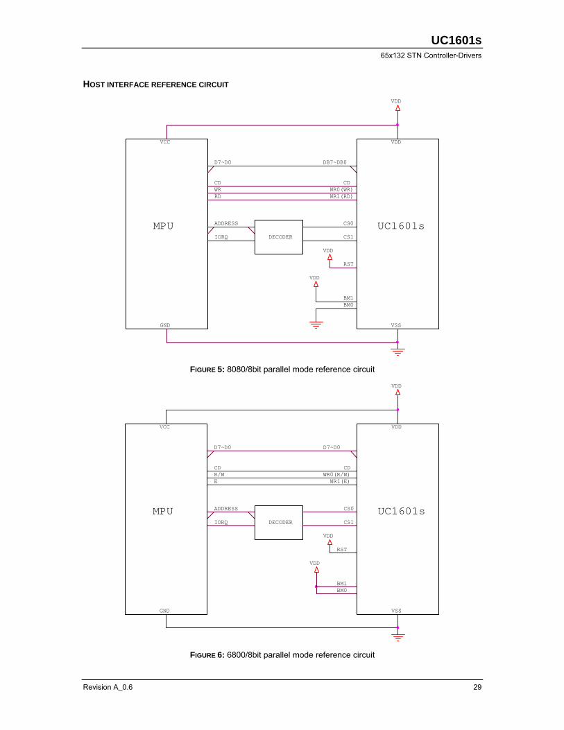
HOST INTERFACE REFERENCE CIRCUIT
VSS
VDD
VCC
MPU
CD
CS0
CS1
WR1(RD)RD
UC1601s
VDD
DB7~DB0
RST
VDD
WR
IORQ
CD
BM1
GND
BM0
VDD
DECODER
WR0(WR)
ADDRESS
D7~D0
FIGURE 5: 8080/8bit parallel mode reference circuit
VDD
UC1601s
BM1
CS1
VDD
VSS
MPU
VCC
VDD
WR0(R/W)
VDD
R/WE WR1(E)
RST
DECODER
D7~D0
GND
BM0
IORQ
CS0ADDRESS
CD
D7~D0
CD
FIGURE 6: 6800/8bit parallel mode reference circuit
ULTRACHIP
High-Voltage Mixed-Signal IC ©1999~2007
30 ES Specifications
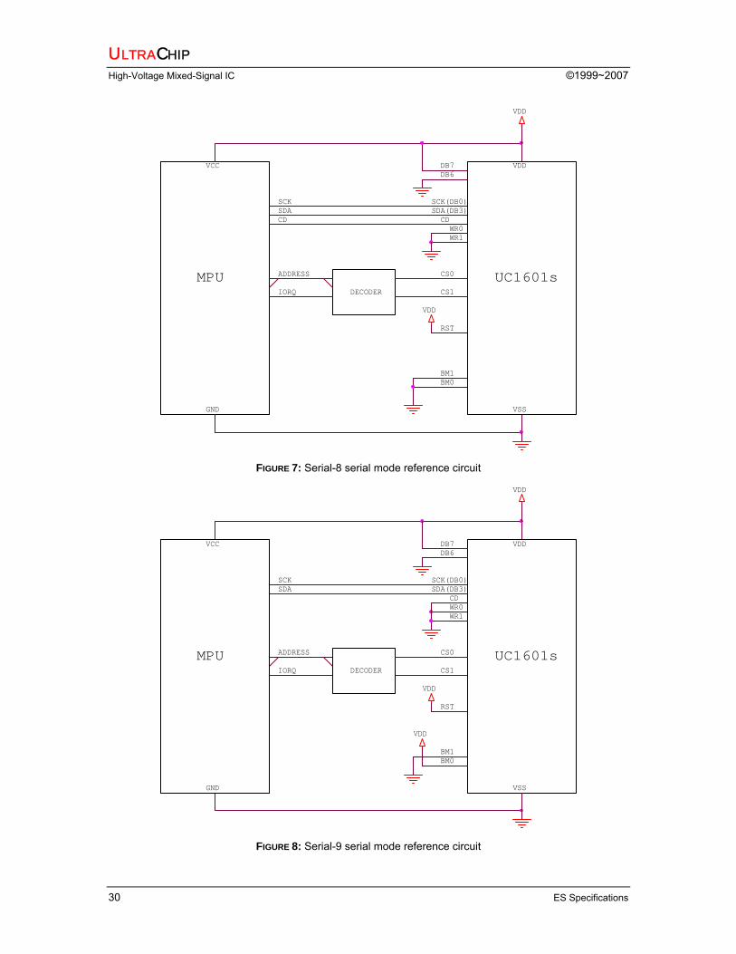
BM0
SCK(DB0)
UC1601s
DB6
CS0
DB7
CDSDA
VDD
VDD
DECODER
RST
WR1
BM1
VDD
ADDRESS
IORQ
VSS
WR0
MPUCS1
GND
CDSDA(DB3)
SCK
VCC
FIGURE 7: Serial-8 serial mode reference circuit
RST
SCK
GND
VDD
DB6
BM0
DB7
SCK(DB0)
DECODER
CS0
WR0
VCC
CS1
SDA(DB3)
VDD
BM1
MPU
SDACD
IORQ
ADDRESS
WR1
VDD
VSS
VDD
UC1601s
FIGURE 8: Serial-9 serial mode reference circuit
UC1601S 65x132 STN Controller-Drivers
Revision A_0.6 31
BM0
UC1601s
SDA(DB3)
RST
VDD
SDA
VDD
VSS
CS1(A3)
DB6R2
BM1
CS0(A2)
DB7VCC
VDD
SCK
GND
SCK(DB0)
R1
WR0CD
VDD
WR1
MPU
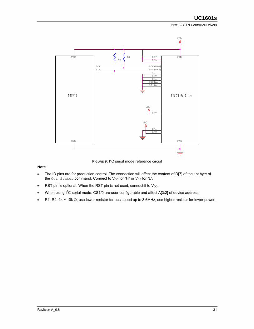
FIGURE 9: I2C serial mode reference circuit
Note
• The ID pins are for production control. The connection will affect the content of D[7] of the 1st byte of the Get Status command. Connect to VDD for “H” or VSS for “L”.
• RST pin is optional. When the RST pin is not used, connect it to VDD.
• When using I2C serial mode, CS1/0 are user configurable and affect A[3:2] of device address.
• R1, R2: 2k ~ 10k Ω, use lower resistor for bus speed up to 3.6MHz, use higher resistor for lower power.
ULTRACHIP
High-Voltage Mixed-Signal IC ©1999~2007
32 ES Specifications
DISPLAY DATA RAM (DDRAM)
DATA ORGANIZATION
The input display data is stored to a dual port static DDRAM (DDRAM, for Display Data RAM) organized as 65x132.
After setting CA and RA, the subsequent data write cycle will store the data for the specified pixel to the proper memory location.
Please refer to the map in the following page between the relation of COM, SEG, SRAM, and various memory control registers.
DISPLAY DATA RAM ACCESS The Display RAM is a special purpose dual port RAM which allows asynchronous access to both its column and row data. Thus, RAM can be independently accessed both for Host Interface and for display operations.
DISPLAY DATA RAM ADDRESSING
A Host Interface (HI) memory access operation starts with specifying Row Address (RA) and Column Address (CA) by issuing Set Row Address and Set Column Address commands.
If wrap-around (WA, AC[0]) is OFF (0), CA will stop increasing after reaching the end of row (131), and system programmers need to set the values of PA and CA explicitly.
If WA is ON (1), when CA reaches end of page, CA will be reset to 0 and PA will increase or decrease, depending on the setting of row Increment Direction (PID, AC[2]). When PA reaches the boundary of RAM (i.e. PA = 0 or 7), PA will be wrapped around to the other end of RAM and continue.
MX IMPLEMENTATION Column Mirroring (MX) is implemented by selecting either (CA) or (131–CA) as the RAM column address. Changing MX affects the data written to the RAM.
Since MX has no effect of the data already stored in RAM, changing MX does not have immediate effect on the displayed pattern. To refresh the display, refresh the data stored in RAM after setting MX.
ROW MAPPING COM electrode scanning orders are not affected by Start Line (SL), Fixed Line (FLT & FLB) or Mirror Y (MY, LC[3]). Visually, register SL having a non-zero value is equivalent to scrolling the LCD display up or down (depends on MY) by SL rows.
RAM ADDRESS GENERATION The mapping of the data stored in the display SRAM and the scanning electrodes can be obtained by combining the fixed Rm scanning sequence and the following RAM address generation formula.
During the display operation, the RAM line address generation can be mathematically represented as following:
For the 1st line period of each field Line = SL Otherwise Line = Mod(Line+1, 64)
Where Mod is the modular operator, and Line is the bit slice line address of RAM to be outputted to column drivers. Line 0 corresponds to the first bit-slice of data in RAM.
The above Line generation formula produce the “loop around” effect as it effectively resets Line to 0 when Line+1 reaches 64.
MY IMPLEMENTATION Row Mirroring (MY) is implemented by reversing the mapping order between row electrodes and RAM, i.e. the mathematical address generation formula becomes:
For the 1st line period of each field Line = Mod(SL + MR -1, 64)
Otherwise Line = Mod(Line-1 , 64)
Visually, the effect of MY is equivalent to flipping the display upside down. The data stored in display RAM is not affected by MY.
UC1601S 65x132 STN Controller-Drivers
Revision A_0.6 33
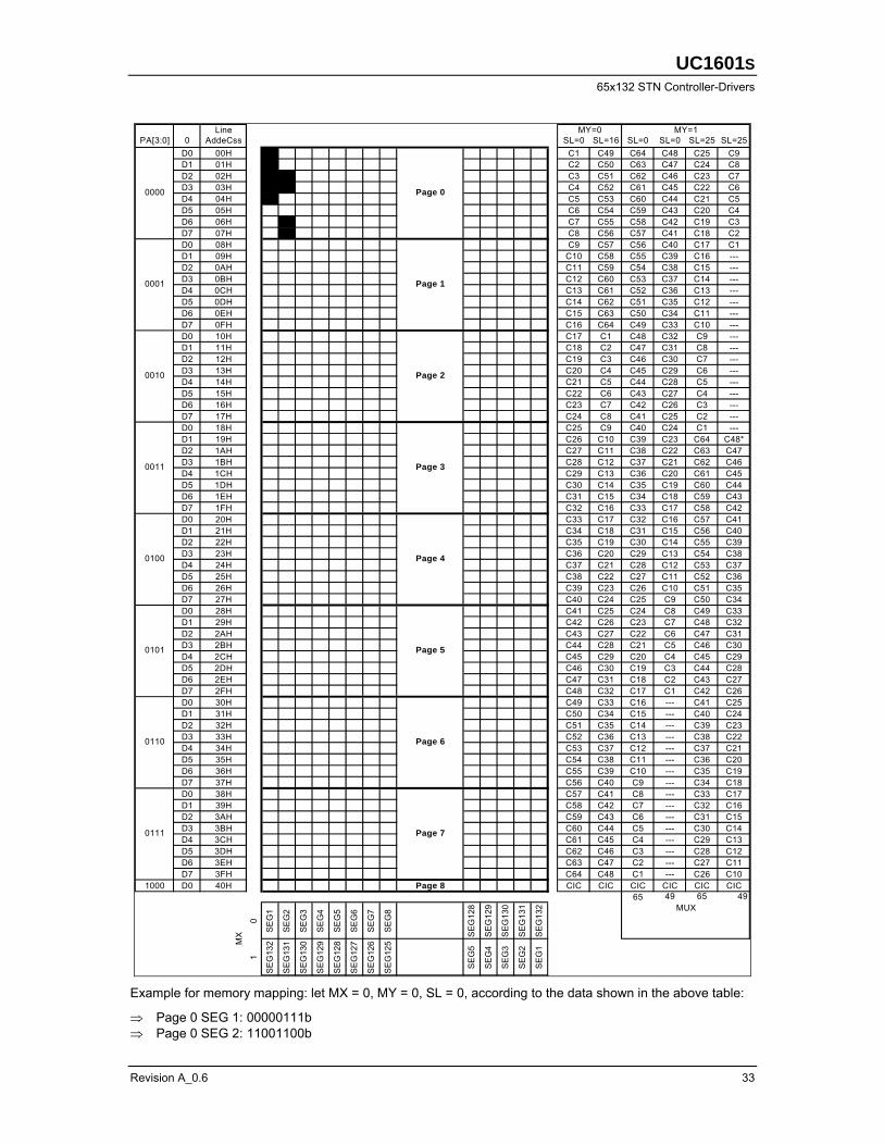
LinePA[3:0] 0 AddeCss SL=0 SL=16 SL=0 SL=0 SL=25 SL=25
D0 00H C1 C49 C64 C48 C25 C9D1 01H C2 C50 C63 C47 C24 C8D2 02H C3 C51 C62 C46 C23 C7D3 03H C4 C52 C61 C45 C22 C6D4 04H C5 C53 C60 C44 C21 C5D5 05H C6 C54 C59 C43 C20 C4D6 06H C7 C55 C58 C42 C19 C3D7 07H C8 C56 C57 C41 C18 C2D0 08H C9 C57 C56 C40 C17 C1D1 09H C10 C58 C55 C39 C16 ---D2 0AH C11 C59 C54 C38 C15 ---D3 0BH C12 C60 C53 C37 C14 ---D4 0CH C13 C61 C52 C36 C13 ---D5 0DH C14 C62 C51 C35 C12 ---D6 0EH C15 C63 C50 C34 C11 ---D7 0FH C16 C64 C49 C33 C10 ---D0 10H C17 C1 C48 C32 C9 ---D1 11H C18 C2 C47 C31 C8 ---D2 12H C19 C3 C46 C30 C7 ---D3 13H C20 C4 C45 C29 C6 ---D4 14H C21 C5 C44 C28 C5 ---D5 15H C22 C6 C43 C27 C4 ---D6 16H C23 C7 C42 C26 C3 ---D7 17H C24 C8 C41 C25 C2 ---D0 18H C25 C9 C40 C24 C1 ---D1 19H C26 C10 C39 C23 C64 C48*D2 1AH C27 C11 C38 C22 C63 C47D3 1BH C28 C12 C37 C21 C62 C46D4 1CH C29 C13 C36 C20 C61 C45D5 1DH C30 C14 C35 C19 C60 C44D6 1EH C31 C15 C34 C18 C59 C43D7 1FH C32 C16 C33 C17 C58 C42D0 20H C33 C17 C32 C16 C57 C41D1 21H C34 C18 C31 C15 C56 C40D2 22H C35 C19 C30 C14 C55 C39D3 23H C36 C20 C29 C13 C54 C38D4 24H C37 C21 C28 C12 C53 C37D5 25H C38 C22 C27 C11 C52 C36D6 26H C39 C23 C26 C10 C51 C35D7 27H C40 C24 C25 C9 C50 C34D0 28H C41 C25 C24 C8 C49 C33D1 29H C42 C26 C23 C7 C48 C32D2 2AH C43 C27 C22 C6 C47 C31D3 2BH C44 C28 C21 C5 C46 C30D4 2CH C45 C29 C20 C4 C45 C29D5 2DH C46 C30 C19 C3 C44 C28D6 2EH C47 C31 C18 C2 C43 C27D7 2FH C48 C32 C17 C1 C42 C26D0 30H C49 C33 C16 --- C41 C25D1 31H C50 C34 C15 --- C40 C24D2 32H C51 C35 C14 --- C39 C23D3 33H C52 C36 C13 --- C38 C22D4 34H C53 C37 C12 --- C37 C21D5 35H C54 C38 C11 --- C36 C20D6 36H C55 C39 C10 --- C35 C19D7 37H C56 C40 C9 --- C34 C18D0 38H C57 C41 C8 --- C33 C17D1 39H C58 C42 C7 --- C32 C16D2 3AH C59 C43 C6 --- C31 C15D3 3BH C60 C44 C5 --- C30 C14D4 3CH C61 C45 C4 --- C29 C13D5 3DH C62 C46 C3 --- C28 C12D6 3EH C63 C47 C2 --- C27 C11D7 3FH C64 C48 C1 --- C26 C10
1000 D0 40H Page 8 CIC CIC CIC CIC CIC CIC65 49 65 49
0
SEG
1
SEG
2
SEG
3
SEG
4
SEG
5
SEG
6
SEG
7
SEG
8
SEG
128
SEG
129
SEG
130
SEG
131
SEG
132
1
SE
G13
2
SE
G13
1
SE
G13
0
SE
G12
9
SE
G12
8
SE
G12
7
SE
G12
6
SE
G12
5
SEG
5
SEG
4
SEG
3
SEG
2
SEG
1
MX
0110
0000
MY=1
Page 7
Page 6
MY=0
Page 4
Page 5
MUX
Page 0
Page 1
Page 2
Page 3
0111
0001
0010
0011
0100
0101
Example for memory mapping: let MX = 0, MY = 0, SL = 0, according to the data shown in the above table:
⇒ Page 0 SEG 1: 00000111b ⇒ Page 0 SEG 2: 11001100b
ULTRACHIP
High-Voltage Mixed-Signal IC ©1999~2007
34 ES Specifications
RESET & POWER MANAGEMENT
TYPES OF RESET UC1601s has two different types of Reset:
Power-ON-Reset and System-Reset.
Power-ON-Reset is performed right after VDD is connected to power. Power-On-Reset will first wait for about ~5mS, depending on the time required for VDD to stabilize, and then trigger the System Reset.
System Reset can also be activated by software command or by connecting RST pin to ground.
In the following discussions, Reset means System Reset.
RESET STATUS When UC1601s enters RESET sequence:
• Operation mode will be “Reset”
• All control registers are reset to default values. Refer to Control Registers for details of their default values.
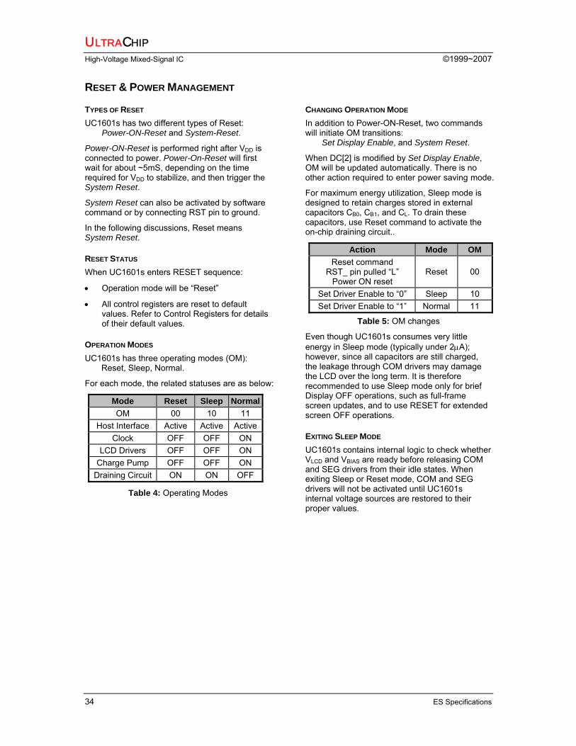
OPERATION MODES UC1601s has three operating modes (OM): Reset, Sleep, Normal.
For each mode, the related statuses are as below:
Mode Reset Sleep NormalOM 00 10 11
Host Interface Active Active ActiveClock OFF OFF ON
LCD Drivers OFF OFF ON Charge Pump OFF OFF ON
Draining Circuit ON ON OFF
Table 4: Operating Modes
CHANGING OPERATION MODE In addition to Power-ON-Reset, two commands will initiate OM transitions: Set Display Enable, and System Reset.
When DC[2] is modified by Set Display Enable, OM will be updated automatically. There is no other action required to enter power saving mode.
For maximum energy utilization, Sleep mode is designed to retain charges stored in external capacitors CB0, CB1, and CL. To drain these capacitors, use Reset command to activate the on-chip draining circuit..
Action Mode OM Reset command
RST_ pin pulled “L” Power ON reset
Reset 00
Set Driver Enable to “0” Sleep 10 Set Driver Enable to “1” Normal 11
Table 5: OM changes
Even though UC1601s consumes very little energy in Sleep mode (typically under 2µA); however, since all capacitors are still charged, the leakage through COM drivers may damage the LCD over the long term. It is therefore recommended to use Sleep mode only for brief Display OFF operations, such as full-frame screen updates, and to use RESET for extended screen OFF operations.
EXITING SLEEP MODE UC1601s contains internal logic to check whether VLCD and VBIAS are ready before releasing COM and SEG drivers from their idle states. When exiting Sleep or Reset mode, COM and SEG drivers will not be activated until UC1601s internal voltage sources are restored to their proper values.
UC1601S 65x132 STN Controller-Drivers
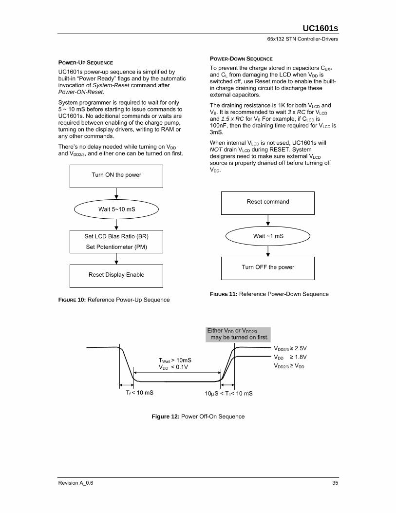
Revision A_0.6 35
POWER-UP SEQUENCE UC1601s power-up sequence is simplified by built-in “Power Ready” flags and by the automatic invocation of System-Reset command after Power-ON-Reset.
System programmer is required to wait for only 5 ~ 10 mS before starting to issue commands to UC1601s. No additional commands or waits are required between enabling of the charge pump, turning on the display drivers, writing to RAM or any other commands.
There’s no delay needed while turning on VDD and VDD2/3, and either one can be turned on first.
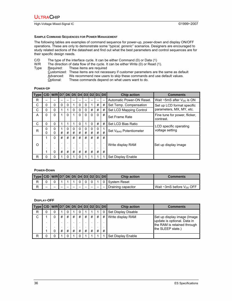
FIGURE 10: Reference Power-Up Sequence
POWER-DOWN SEQUENCE To prevent the charge stored in capacitors CBX+ and CL from damaging the LCD when VDD is switched off, use Reset mode to enable the built-in charge draining circuit to discharge these external capacitors.
The draining resistance is 1K for both VLCD and VB. It is recommended to wait 3 x RC for VLCD and 1.5 x RC for VB For example, if CLCD is 100nF, then the draining time required for VLCD is 3mS.
When internal VLCD is not used, UC1601s will NOT drain VLCD during RESET. System designers need to make sure external VLCD source is properly drained off before turning off VDD.
FIGURE 11: Reference Power-Down Sequence
Figure 12: Power Off-On Sequence
10µS < T1< 10 mS Tf < 10 mS
VDD2/3 ≥ 2.5V VDD ≥ 1.8V VDD2/3 ≥ VDD
Either VDD or VDD2/3 may be turned on first.
TWait > 10mS VDD < 0.1V
Reset command
Turn OFF the power
Wait ~1 mS
Turn ON the power
Set LCD Bias Ratio (BR)
Set Potentiometer (PM)
Reset Display Enable
Wait 5~10 mS
ULTRACHIP
High-Voltage Mixed-Signal IC ©1999~2007
36 ES Specifications
SAMPLE COMMAND SEQUENCES FOR POWER MANAGEMENT The following tables are examples of command sequence for power-up, power-down and display ON/OFF operations. These are only to demonstrate some “typical, generic” scenarios. Designers are encouraged to study related sections of the datasheet and find out what the best parameters and control sequences are for their specific design needs.
C/D The type of the interface cycle. It can be either Command (0) or Data (1) W/R The direction of data flow of the cycle. It can be either Write (0) or Read (1). Type Required: These items are required
Customized: These items are not necessary if customer parameters are the same as default Advanced: We recommend new users to skip these commands and use default values. Optional: These commands depend on what users want to do.
POWER-UP
Type C/D W/R D7 D6 D5 D4 D3 D2 D1 D0 Chip action Comments R – – – – – – – – – – Automatic Power-ON Reset. Wait ~5mS after VDD is ON C 0 0 0 0 1 0 0 1 # # Set Temp. Compensation C 0 0 1 1 0 0 0 # # # Set LCD Mapping Control
Set up LCD format specific parameters, MX, MY, etc.
A 0 0 1 0 1 0 0 0 0 # Set Frame Rate Fine tune for power, flicker, contrast.
C 0 0 1 1 1 0 1 0 # # Set LCD Bias Ratio
R 0 0
0 0
1 #
0 #
0 #
0 #
0 #
0 #
0#
1# Set VBIAS Potentiometer
LCD specific operating voltage setting
O
1 . . 1
0 . . 0
# . . #
# . . #
# . . #
# . . #
# . . #
# . . #
#..#
#..#
Write display RAM Set up display image
R 0 0 1 0 1 0 1 1 1 1 Set Display Enable
POWER-DOWN
Type C/D W/R D7 D6 D5 D4 D3 D2 D1 D0 Chip action Comments R 0 0 1 1 1 0 0 0 1 0 System Reset R – – – – – – – – – – Draining capacitor Wait ~3mS before VDD OFF
DISPLAY-OFF
Type C/D W/R D7 D6 D5 D4 D3 D2 D1 D0 Chip action Comments R 0 0 1 0 1 0 1 1 1 0 Set Display Disable C 1
.
. 1
0 . . 0
# . . #
# . . #
# . . #
# . . #
# . . #
# . . #
#..#
#..#
Write display RAM Set up display image (Image update is optional. Data in the RAM is retained through the SLEEP state.)
R 0 0 1 0 1 0 1 1 1 1 Set Display Enable
UC1601S 65x132 STN Controller-Drivers
Revision A_0.6 37
ESD CONSIDERATION UC1600 series products usually are provided in bare die format to customers. This makes the product particularly sensitive to ESD damage during handling and manufacturing process. It is, therefore, highly recommended that LCM makers strictly follow the "JESD 625-A Requirements for Handling Electrostatic-Discharge-Sensitive (ESDS) Devices" when manufacturing LCM.
The following pins in UC1601s require special "ESD Sensitivity" consideration in particular:
Machine Mode Human Body Mode Test Mode
Pins VDD VSS VDD VSS
LCD Driver 225V 250V 3.0KV 3.0KV
LCM Digital Interface 300V 300V 3.0KV 3.0KV
TST1/2/4 300V 300V 3.0KV 3.0KV
CB pins 300V 300V 3.0KV 3.0KV
VLCDIN 300V 300V 3.0KV 3.0KV LCM HV Interface
VLCDOUT 300V 300V 3.0KV 3.0KV
PWR/GND -- 300V -- 3.0KV
According to UltraChip's Mass Production experiences, the ESD tolerance conditions are believed to be very stable and can produce high yield in multiple customer sites. However, special care is still required during handling and manufacturing process to avoid unnecessary yield loss due to ESD damages.
ULTRACHIP
High-Voltage Mixed-Signal IC ©1999~2007
38 ES Specifications
ABSOLUTE MAXIMUM RATINGS In accordance with IEC134 - notes 1, 2 and 3.
Symbol Parameter Min. Max. UnitVDD Logic Supply voltage -0.3 +4.0 V
VDD2 LCD Generator Supply voltage -0.3 +4.0 V
VDD3 Analog Circuit Supply voltage -0.3 +4.0 V
VDD2/3-VDD Voltage difference between VDD and VDD2/3 -- 1.2 V
VLCD LCD Generated voltage -0.3 +13.2 V
VIN / VOUT Any input/output -0.4 VDD + 0.3 V
TOPR Operating temperature range -30 +85 oC
TSTR Storage temperature -55 +125 oC
Notes 1. VDD is based on VSS = 0V
2. Stress values listed above may cause permanent damages to the device.
UC1601S 65x132 STN Controller-Drivers
Revision A_0.6 39
SPECIFICATIONS
DC CHARACTERISTICS
Symbol Parameter Conditions Min. Typ. Max. Unit VDD Supply for digital circuit 1.65 3.3 V
VDD2/3 Supply for bias & pump 2.4 3.3 V
VLCD Charge pump output VDD2/3 2.4V, 25OC 11.5 V
VD LCD data voltage VDD2/3 2.4V, 25OC 0.80 1.32 V
VIL Input logic LOW 0.2VDD V
VIH Input logic HIGH 0.8VDD V
VOL Output logic LOW 0.2VDD V
VOH Output logic HIGH 0.8VDD V
IIL Input leakage current 1.5 µA
ISB Standby current VDD = VDD2/3 = 3.3V, Temp = 85oC 50 µA
CIN Input capacitance 5 10 PF
COUT Output capacitance 5 10 PF
R0(SEG) SEG output impedance VLCD = 11V 2000 3000 Ω
R0(COM) COM output impedance VLCD = 11V 2000 3000 Ω
FFR Average Frame Rate LC[3] = 0b -10% 80 +10% Hz
POWER CONSUMPTION VDD = 2.7V, Bias Ratio = 11b, PM =192, VLCD = 10.73 V Frame Rate = 0b, Panel Loading (PC[0]) 0 b, Mux Rate = 65, Bus mode =6800, CL =330 nF, CB = 2.2 µF Temperature = 25oC, All outputs are open circuit.
Display Pattern Conditions Typ. Max. All-OFF Bus = idle 223 (TBD)
2-pixel checker Bus = idle 239 (TBD)
- Bus = idle (standby current) - 5
ULTRACHIP
High-Voltage Mixed-Signal IC ©1999~2007
40 ES Specifications
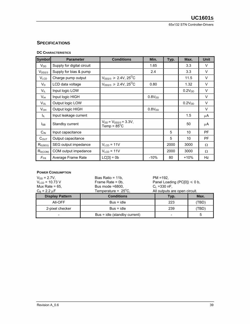
AC CHARACTERISTICS
FIGURE 13: Parallel Bus Timing Characteristics (for 8080 MCU)
(2.5V VDD < 3.3V, Ta= –30 to +85oC)
Symbol Signal Description Condition Min. Max. UnitstAS80 tAH80
CD Address setup time Address hold time
0 0
– nS
tCY80
System cycle time (read) (write)
120 80
– nS
tPWR80 WR1 Pulse width (read) 60 – nS tPWW80 WR0 Pulse width (write) 40 – nS tHPW80
WR0, WR1 High pulse width
(read) (write)
60 40
– nS
tDS80 tDH80
D0~D7 Data setup time Data hold time
30 0
– nS
tACC80 tOD80
Read access time Output disable time
CL = 100pF – 15
60 30
nS
tCSSA80 tCSH80
CS1/CS0 Chip select setup time 5 5
nS
CD tAS80 tAH80 CS0 CS1 tCSSA80 tCY80 tCSH80 tCSSD80 tPWR80, tPWW80 tHPW80 WR0 WR1
tDS80 tDH80
Write D[7:0] tACC80 tOD80 Read D[7:0]
UC1601S 65x132 STN Controller-Drivers
Revision A_0.6 41
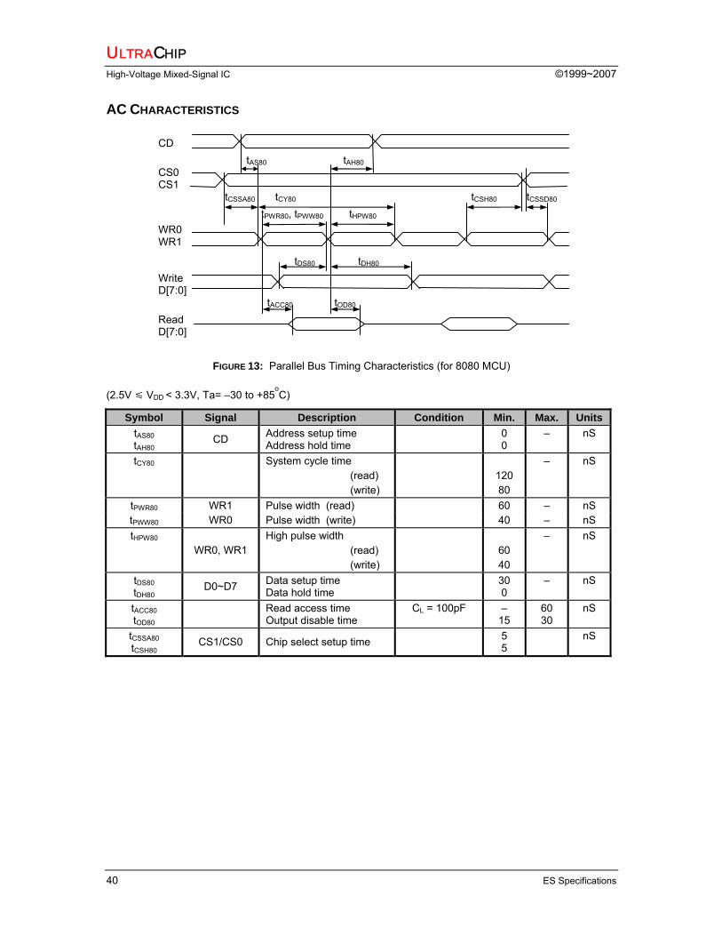
(1.65V VDD < 2.5V, Ta= –30 to +85oC)
Symbol Signal Description Condition Min. Max. UnitstAS80 tAH80
CD Address setup time Address hold time
0 0
– nS
tCY80
System cycle time (read)(write)
240 160
– nS
tPWR80 WR1 Pulse width (read) 120 – nS tPWW80 WR0 Pulse width (write) 80 – nS tHPW80
WR0, WR1 High pulse width
(read) (write)
120 80
– nS
tDS80 tDH80
D0~D7 Data setup time Data hold time
60 0
– nS
tACC80 tOD80
Read access time Output disable time
CL = 100pF – 15
60 30
nS
tCSSA80 tCSH80
CS1/CS0 Chip select setup time 5 5
nS
ULTRACHIP
High-Voltage Mixed-Signal IC ©1999~2007
42 ES Specifications
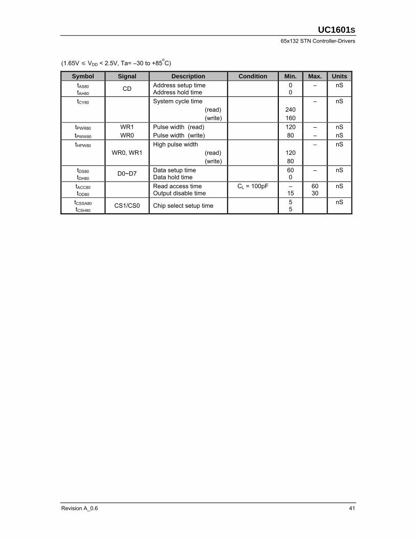
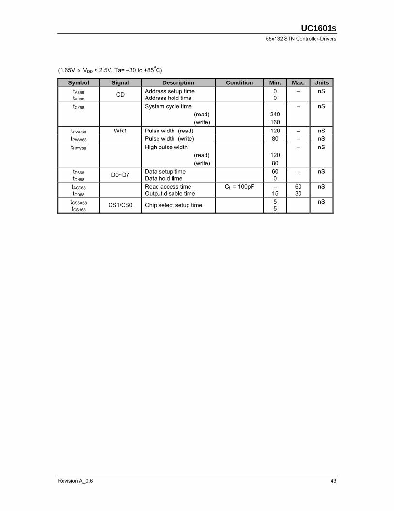
FIGURE 14: Parallel Bus Timing Characteristics (for 6800 MCU)
(2.5V VDD < 3.3V, Ta= –30 to +85oC)
Symbol Signal Description Condition Min. Max. UnitstAS68 tAH68
CD Address setup time Address hold time
0 0
– nS
tCY68
System cycle time (read)(write)
120 80
– nS
tPWR68 WR1 Pulse width (read) 60 – nS tPWW68 Pulse width (write) 40 – nS tHPW68
High pulse width
(read) (write)
60 40
– nS
tDS68 tDH68
D0~D7 Data setup time Data hold time
30 0
– nS
tACC68 tOD68
Read access time Output disable time
CL = 100pF – 15
60 30
nS
tCSSA68 tCSH68
CS1/CS0 Chip select setup time 5 5
nS
CD tAS68 tAH68 CS0 CS1
tCSSA68 tCY68 tCSH68 tCSSD68 tPWR68, tPWW68 tLPW68 WR1
tDS68 tDH68
Write D[7:0] tACC68 tOD68 Read D[7:0]
UC1601S 65x132 STN Controller-Drivers
Revision A_0.6 43
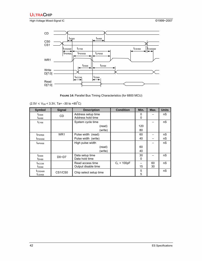
(1.65V VDD < 2.5V, Ta= –30 to +85oC)
Symbol Signal Description Condition Min. Max. UnitstAS68 tAH68
CD Address setup time Address hold time
0 0
– nS
tCY68
System cycle time (read)(write)
240 160
– nS
tPWR68 WR1 Pulse width (read) 120 – nS tPWW68 Pulse width (write) 80 – nS tHPW68
High pulse width
(read)(write)
120 80
– nS
tDS68 tDH68
D0~D7 Data setup time Data hold time
60 0
– nS
tACC68 tOD68
Read access time Output disable time
CL = 100pF – 15
60 30
nS
tCSSA68 tCSH68
CS1/CS0 Chip select setup time 5 5
nS
ULTRACHIP
High-Voltage Mixed-Signal IC ©1999~2007
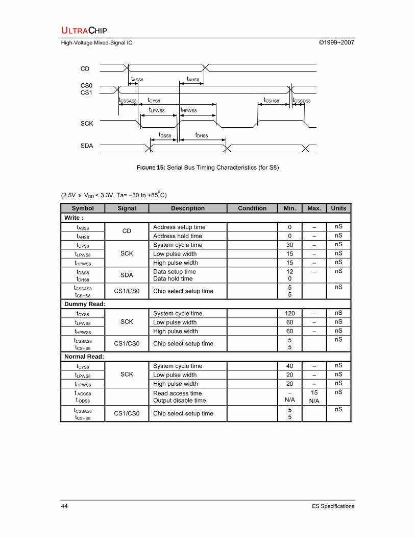
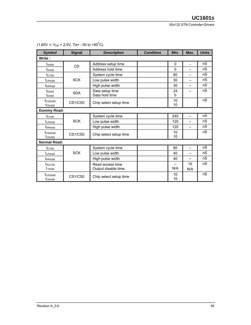
44 ES Specifications
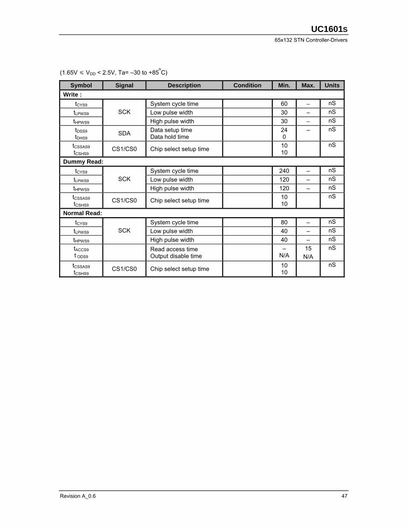
FIGURE 15: Serial Bus Timing Characteristics (for S8)
(2.5V VDD < 3.3V, Ta= –30 to +85oC)
Symbol Signal Description Condition Min. Max. UnitsWrite :
tASS8 Address setup time 0 – nS tAHS8
CD Address hold time 0 – nS
tCYS8 System cycle time 30 – nS tLPWS8 Low pulse width 15 – nS tHPWS8
SCK High pulse width 15 – nS
tDSS8 tDHS8
SDA Data setup time Data hold time
12 0
– nS
tCSSAS8 tCSHS8
CS1/CS0 Chip select setup time 5 5
nS
Dummy Read: tCYS8 System cycle time 120 – nS tLPWS8 Low pulse width 60 – nS tHPWS8
SCK High pulse width 60 – nS
tCSSAS8 tCSHS8
CS1/CS0 Chip select setup time 5 5
nS
Normal Read: tCYS8 System cycle time 40 – nS tLPWS8 Low pulse width 20 – nS tHPWS8
SCK High pulse width 20 – nS
t ACCS8 t ODS8 Read access time
Output disable time
– N/A
15 N/A
nS
tCSSAS8 tCSHS8
CS1/CS0 Chip select setup time 5 5
nS
CD tASS8 tAHS8 CS0 CS1 tCSSAS8 tCYS8 tCSHS8 tCSSDS8 tLPWS8 tHPWS8 SCK
tDSS8 tDHS8
SDA
UC1601S 65x132 STN Controller-Drivers
Revision A_0.6 45
(1.65V VDD < 2.5V, Ta= –30 to +85oC)
Symbol Signal Description Condition Min. Max. UnitsWrite :
tASS8 Address setup time 0 – nS tAHS8
CD Address hold time 0 – nS
tCYS8 System cycle time 60 – nS tLPWS8 Low pulse width 30 – nS tHPWS8
SCK High pulse width 30 – nS
tDSS8 tDHS8
SDA Data setup time Data hold time
24 0
– nS
tCSSAS8 tCSHS8
CS1/CS0 Chip select setup time 10 10
nS
Dummy Read: tCYS8 System cycle time 240 – nS tLPWS8 Low pulse width 120 – nS tHPWS8
SCK High pulse width 120 – nS
tCSSAS8 tCSHS8
CS1/CS0 Chip select setup time 10 10
nS
Normal Read: tCYS8 System cycle time 80 – nS tLPWS8 Low pulse width 40 – nS tHPWS8
SCK High pulse width 40 – nS
tACCS8 t ODS8 Read access time
Output disable time
– N/A
15 N/A
nS
tCSSAS8 tCSHS8
CS1/CS0 Chip select setup time 10 10
nS
ULTRACHIP
High-Voltage Mixed-Signal IC ©1999~2007
46 ES Specifications
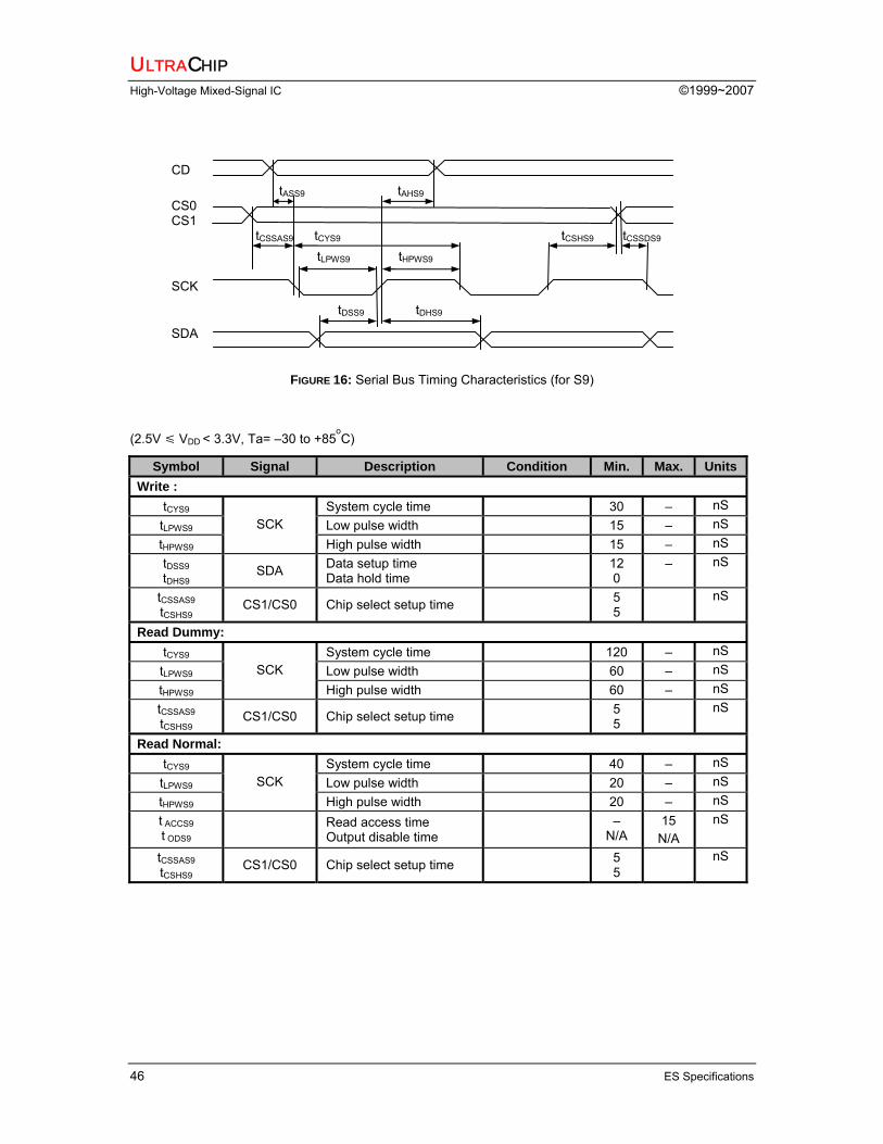
FIGURE 16: Serial Bus Timing Characteristics (for S9)
(2.5V VDD < 3.3V, Ta= –30 to +85oC)
Symbol Signal Description Condition Min. Max. UnitsWrite :
tCYS9 System cycle time 30 – nS tLPWS9 Low pulse width 15 – nS tHPWS9
SCK High pulse width 15 – nS
tDSS9 tDHS9
SDA Data setup time Data hold time
12 0
– nS
tCSSAS9 tCSHS9
CS1/CS0 Chip select setup time 5 5
nS
Read Dummy: tCYS9 System cycle time 120 – nS tLPWS9 Low pulse width 60 – nS tHPWS9
SCK High pulse width 60 – nS
tCSSAS9 tCSHS9
CS1/CS0 Chip select setup time 5 5
nS
Read Normal: tCYS9 System cycle time 40 – nS tLPWS9 Low pulse width 20 – nS tHPWS9
SCK High pulse width 20 – nS
t ACCS9 t ODS9 Read access time
Output disable time
– N/A
15 N/A
nS
tCSSAS9 tCSHS9
CS1/CS0 Chip select setup time 5 5
nS
CD tASS9 tAHS9 CS0 CS1 tCSSAS9 tCYS9 tCSHS9 tCSSDS9 tLPWS9 tHPWS9 SCK
tDSS9 tDHS9
SDA
UC1601S 65x132 STN Controller-Drivers
Revision A_0.6 47
(1.65V VDD < 2.5V, Ta= –30 to +85oC)
Symbol Signal Description Condition Min. Max. UnitsWrite :
tCYS9 System cycle time 60 – nS tLPWS9 Low pulse width 30 – nS tHPWS9
SCK High pulse width 30 – nS
tDSS9 tDHS9
SDA Data setup time Data hold time
24 0
– nS
tCSSAS9 tCSHS9
CS1/CS0 Chip select setup time 10 10
nS
Dummy Read: tCYS9 System cycle time 240 – nS tLPWS9 Low pulse width 120 – nS tHPWS9
SCK High pulse width 120 – nS
tCSSAS9 tCSHS9
CS1/CS0 Chip select setup time 10 10
nS
Normal Read: tCYS9 System cycle time 80 – nS tLPWS9 Low pulse width 40 – nS tHPWS9
SCK High pulse width 40 – nS
tACCS9 t ODS9 Read access time
Output disable time
– N/A
15 N/A
nS
tCSSAS9 tCSHS9
CS1/CS0 Chip select setup time 10 10
nS
ULTRACHIP
High-Voltage Mixed-Signal IC ©1999~2007
48 ES Specifications
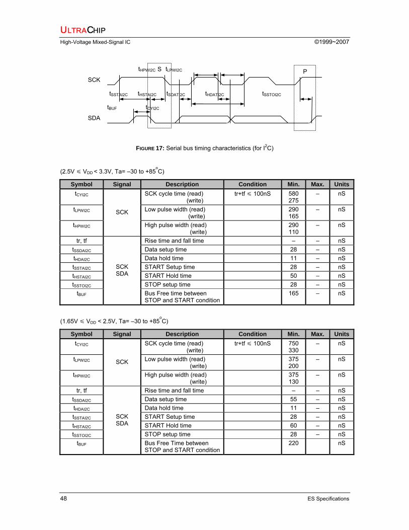
FIGURE 17: Serial bus timing characteristics (for I2C)
(2.5V VDD < 3.3V, Ta= –30 to +85oC)
Symbol Signal Description Condition Min. Max. UnitstCYI2C SCK cycle time (read)
(write) tr+tf 100nS 580
275 – nS
tLPWI2C Low pulse width (read) (write)
290 165
– nS
tHPWI2C
SCK
High pulse width (read) (write)
290 110
– nS
tr, tf Rise time and fall time – – nS tSSDAI2C Data setup time 28 – nS tHDAI2C Data hold time 11 – nS tSSTAI2C START Setup time 28 – nS tHSTAI2C START Hold time 50 – nS tSSTOI2C STOP setup time 28 – nS
tBUF
SCK SDA
Bus Free time between STOP and START condition
165 – nS
(1.65V VDD < 2.5V, Ta= –30 to +85oC)
Symbol Signal Description Condition Min. Max. UnitstCYI2C SCK cycle time (read)
(write) tr+tf 100nS 750
330 – nS
tLPWI2C Low pulse width (read) (write)
375 200
– nS
tHPWI2C
SCK
High pulse width (read) (write)
375 130
– nS
tr, tf Rise time and fall time – – nS tSSDAI2C Data setup time 55 – nS tHDAI2C Data hold time 11 – nS tSSTAI2C START Setup time 28 – nS tHSTAI2C START Hold time 60 – nS tSSTOI2C STOP setup time 28 – nS
tBUF
SCK SDA
Bus Free Time between STOP and START condition
220 nS
S tHPWI2C tLPWI2C
SCK
tSSTAI2C tHSTAI2C tSDATI2C tHDATI2C tSSTOI2C
tBUF tCYI2C
SDA
P
UC1601S 65x132 STN Controller-Drivers
Revision A_0.6 49
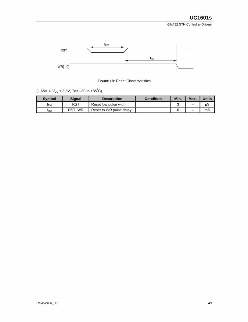
RST
tRW
WR[1:0]
tRD
FIGURE 18: Reset Characteristics
(1.65V VDD < 3.3V, Ta= –30 to +85oC)
Symbol Signal Description Condition Min. Max. UnitstRW RST Reset low pulse width 3 – µS tRD RST, WR Reset to WR pulse delay 6 – mS
ULTRACHIP
High-Voltage Mixed-Signal IC ©1999~2007
50 ES Specifications
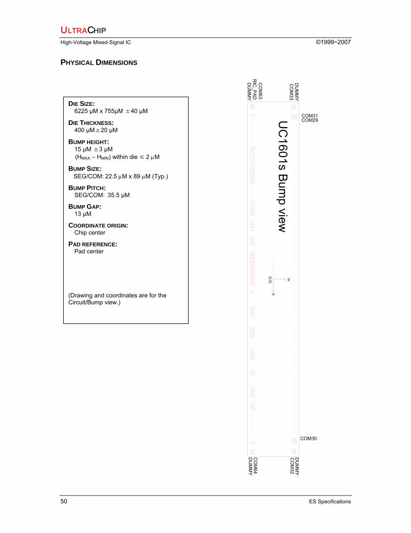
PHYSICAL DIMENSIONS
DU
MM
Y
COM31COM29
CO
M63
CO
M33
UC
1601s Bum
p view
DU
MM
Y
RIC
_PA
D
Y(0,0)X
COM30
DU
MM
Y
CO
M32
DU
MM
YC
OM
64
DIE SIZE: 6225 µM x 755µM ±40 µM
DIE THICKNESS: 400 µM±20 µM
BUMP HEIGHT: 15 µM ±3 µM
(HMAX – HMIN) within die 2 µM
BUMP SIZE: SEG/COM: 22.5 µM x 89 µM (Typ.)
BUMP PITCH: SEG/COM: 35.5 µM
BUMP GAP: 13 µM
COORDINATE ORIGIN: Chip center
PAD REFERENCE: Pad center
(Drawing and coordinates are for the Circuit/Bump view.)
UC1601S 65x132 STN Controller-Drivers
Revision A_0.6 51
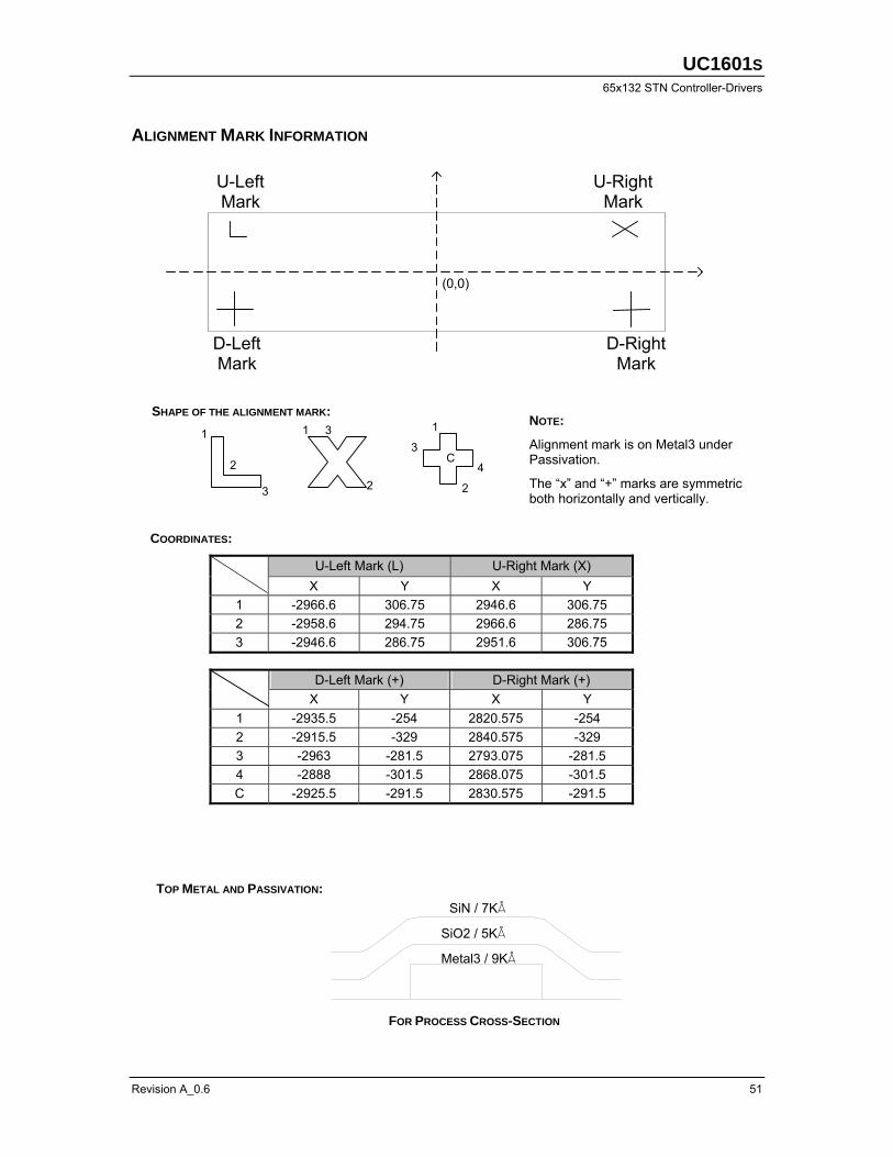
ALIGNMENT MARK INFORMATION
SHAPE OF THE ALIGNMENT MARK:
TOP METAL AND PASSIVATION:
FOR PROCESS CROSS-SECTION
Metal3 / 9KÅ
SiO2 / 5KÅ
SiN / 7KÅ
NOTE:
Alignment mark is on Metal3 under Passivation.
The “x” and “+” marks are symmetric both horizontally and vertically.
COORDINATES:
U-Left Mark (L) U-Right Mark (X) X Y X Y
1 -2966.6 306.75 2946.6 306.75 2 -2958.6 294.75 2966.6 286.75 3 -2946.6 286.75 2951.6 306.75
D-Left Mark (+) D-Right Mark (+)
X Y X Y 1 -2935.5 -254 2820.575 -254 2 -2915.5 -329 2840.575 -329 3 -2963 -281.5 2793.075 -281.5 4 -2888 -301.5 2868.075 -301.5 C -2925.5 -291.5 2830.575 -291.5
Mark Mark
(0,0)
D-Left D-Right
U-Left Mark
U-Right Mark
1
2
3
1
2
3 1
2
3
4C
ULTRACHIP
High-Voltage Mixed-Signal IC ©1999~2007
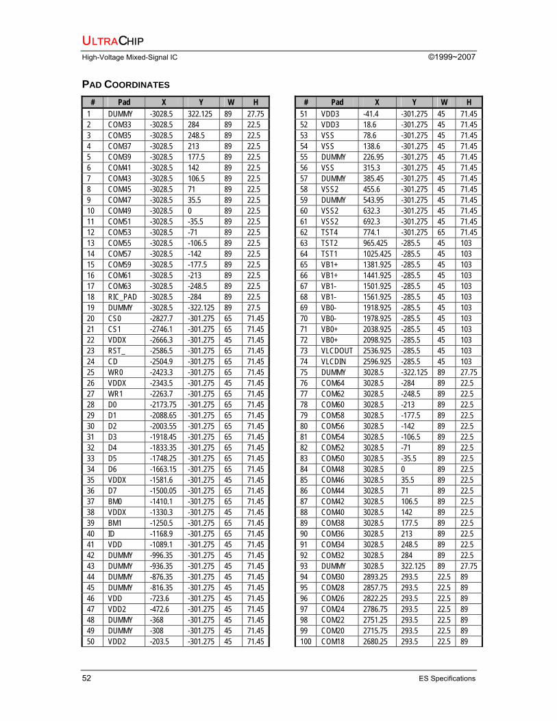
52 ES Specifications
PAD COORDINATES # Pad X Y W H
1 DUMMY -3028.5 322.125 89 27.75 2 COM33 -3028.5 284 89 22.5 3 COM35 -3028.5 248.5 89 22.5 4 COM37 -3028.5 213 89 22.5 5 COM39 -3028.5 177.5 89 22.5 6 COM41 -3028.5 142 89 22.5 7 COM43 -3028.5 106.5 89 22.5 8 COM45 -3028.5 71 89 22.5 9 COM47 -3028.5 35.5 89 22.5 10 COM49 -3028.5 0 89 22.5 11 COM51 -3028.5 -35.5 89 22.5 12 COM53 -3028.5 -71 89 22.5 13 COM55 -3028.5 -106.5 89 22.5 14 COM57 -3028.5 -142 89 22.5 15 COM59 -3028.5 -177.5 89 22.5 16 COM61 -3028.5 -213 89 22.5 17 COM63 -3028.5 -248.5 89 22.5 18 RIC_PAD -3028.5 -284 89 22.5 19 DUMMY -3028.5 -322.125 89 27.5 20 CS0 -2827.7 -301.275 65 71.45 21 CS1 -2746.1 -301.275 65 71.45 22 VDDX -2666.3 -301.275 45 71.45 23 RST_ -2586.5 -301.275 65 71.45 24 CD -2504.9 -301.275 65 71.45 25 WR0 -2423.3 -301.275 65 71.45 26 VDDX -2343.5 -301.275 45 71.45 27 WR1 -2263.7 -301.275 65 71.45 28 D0 -2173.75 -301.275 65 71.45 29 D1 -2088.65 -301.275 65 71.45 30 D2 -2003.55 -301.275 65 71.45 31 D3 -1918.45 -301.275 65 71.45 32 D4 -1833.35 -301.275 65 71.45 33 D5 -1748.25 -301.275 65 71.45 34 D6 -1663.15 -301.275 65 71.45 35 VDDX -1581.6 -301.275 45 71.45 36 D7 -1500.05 -301.275 65 71.45 37 BM0 -1410.1 -301.275 65 71.45 38 VDDX -1330.3 -301.275 45 71.45 39 BM1 -1250.5 -301.275 65 71.45 40 ID -1168.9 -301.275 65 71.45 41 VDD -1089.1 -301.275 45 71.45 42 DUMMY -996.35 -301.275 45 71.45 43 DUMMY -936.35 -301.275 45 71.45 44 DUMMY -876.35 -301.275 45 71.45 45 DUMMY -816.35 -301.275 45 71.45 46 VDD -723.6 -301.275 45 71.45 47 VDD2 -472.6 -301.275 45 71.45 48 DUMMY -368 -301.275 45 71.45 49 DUMMY -308 -301.275 45 71.45 50 VDD2 -203.5 -301.275 45 71.45
# Pad X Y W H 51 VDD3 -41.4 -301.275 45 71.45 52 VDD3 18.6 -301.275 45 71.45 53 VSS 78.6 -301.275 45 71.45 54 VSS 138.6 -301.275 45 71.45 55 DUMMY 226.95 -301.275 45 71.45 56 VSS 315.3 -301.275 45 71.45 57 DUMMY 385.45 -301.275 45 71.45 58 VSS2 455.6 -301.275 45 71.45 59 DUMMY 543.95 -301.275 45 71.45 60 VSS2 632.3 -301.275 45 71.45 61 VSS2 692.3 -301.275 45 71.45 62 TST4 774.1 -301.275 65 71.45 63 TST2 965.425 -285.5 45 103 64 TST1 1025.425 -285.5 45 103 65 VB1+ 1381.925 -285.5 45 103 66 VB1+ 1441.925 -285.5 45 103 67 VB1- 1501.925 -285.5 45 103 68 VB1- 1561.925 -285.5 45 103 69 VB0- 1918.925 -285.5 45 103 70 VB0- 1978.925 -285.5 45 103 71 VB0+ 2038.925 -285.5 45 103 72 VB0+ 2098.925 -285.5 45 103 73 VLCDOUT 2536.925 -285.5 45 103 74 VLCDIN 2596.925 -285.5 45 103 75 DUMMY 3028.5 -322.125 89 27.75 76 COM64 3028.5 -284 89 22.5 77 COM62 3028.5 -248.5 89 22.5 78 COM60 3028.5 -213 89 22.5 79 COM58 3028.5 -177.5 89 22.5 80 COM56 3028.5 -142 89 22.5 81 COM54 3028.5 -106.5 89 22.5 82 COM52 3028.5 -71 89 22.5 83 COM50 3028.5 -35.5 89 22.5 84 COM48 3028.5 0 89 22.5 85 COM46 3028.5 35.5 89 22.5 86 COM44 3028.5 71 89 22.5 87 COM42 3028.5 106.5 89 22.5 88 COM40 3028.5 142 89 22.5 89 COM38 3028.5 177.5 89 22.5 90 COM36 3028.5 213 89 22.5 91 COM34 3028.5 248.5 89 22.5 92 COM32 3028.5 284 89 22.5 93 DUMMY 3028.5 322.125 89 27.75 94 COM30 2893.25 293.5 22.5 89 95 COM28 2857.75 293.5 22.5 89 96 COM26 2822.25 293.5 22.5 89 97 COM24 2786.75 293.5 22.5 89 98 COM22 2751.25 293.5 22.5 89 99 COM20 2715.75 293.5 22.5 89 100 COM18 2680.25 293.5 22.5 89
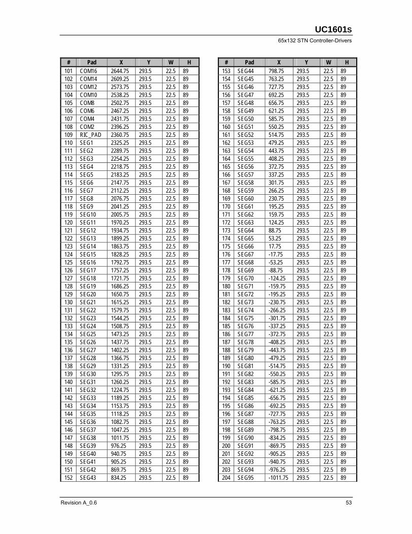
UC1601S 65x132 STN Controller-Drivers
Revision A_0.6 53
# Pad X Y W H 101 COM16 2644.75 293.5 22.5 89 102 COM14 2609.25 293.5 22.5 89 103 COM12 2573.75 293.5 22.5 89 104 COM10 2538.25 293.5 22.5 89 105 COM8 2502.75 293.5 22.5 89 106 COM6 2467.25 293.5 22.5 89 107 COM4 2431.75 293.5 22.5 89 108 COM2 2396.25 293.5 22.5 89 109 RIC_PAD 2360.75 293.5 22.5 89 110 SEG1 2325.25 293.5 22.5 89 111 SEG2 2289.75 293.5 22.5 89 112 SEG3 2254.25 293.5 22.5 89 113 SEG4 2218.75 293.5 22.5 89 114 SEG5 2183.25 293.5 22.5 89 115 SEG6 2147.75 293.5 22.5 89 116 SEG7 2112.25 293.5 22.5 89 117 SEG8 2076.75 293.5 22.5 89 118 SEG9 2041.25 293.5 22.5 89 119 SEG10 2005.75 293.5 22.5 89 120 SEG11 1970.25 293.5 22.5 89 121 SEG12 1934.75 293.5 22.5 89 122 SEG13 1899.25 293.5 22.5 89 123 SEG14 1863.75 293.5 22.5 89 124 SEG15 1828.25 293.5 22.5 89 125 SEG16 1792.75 293.5 22.5 89 126 SEG17 1757.25 293.5 22.5 89 127 SEG18 1721.75 293.5 22.5 89 128 SEG19 1686.25 293.5 22.5 89 129 SEG20 1650.75 293.5 22.5 89 130 SEG21 1615.25 293.5 22.5 89 131 SEG22 1579.75 293.5 22.5 89 132 SEG23 1544.25 293.5 22.5 89 133 SEG24 1508.75 293.5 22.5 89 134 SEG25 1473.25 293.5 22.5 89 135 SEG26 1437.75 293.5 22.5 89 136 SEG27 1402.25 293.5 22.5 89 137 SEG28 1366.75 293.5 22.5 89 138 SEG29 1331.25 293.5 22.5 89 139 SEG30 1295.75 293.5 22.5 89 140 SEG31 1260.25 293.5 22.5 89 141 SEG32 1224.75 293.5 22.5 89 142 SEG33 1189.25 293.5 22.5 89 143 SEG34 1153.75 293.5 22.5 89 144 SEG35 1118.25 293.5 22.5 89 145 SEG36 1082.75 293.5 22.5 89 146 SEG37 1047.25 293.5 22.5 89 147 SEG38 1011.75 293.5 22.5 89 148 SEG39 976.25 293.5 22.5 89 149 SEG40 940.75 293.5 22.5 89 150 SEG41 905.25 293.5 22.5 89 151 SEG42 869.75 293.5 22.5 89 152 SEG43 834.25 293.5 22.5 89
# Pad X Y W H 153 SEG44 798.75 293.5 22.5 89 154 SEG45 763.25 293.5 22.5 89 155 SEG46 727.75 293.5 22.5 89 156 SEG47 692.25 293.5 22.5 89 157 SEG48 656.75 293.5 22.5 89 158 SEG49 621.25 293.5 22.5 89 159 SEG50 585.75 293.5 22.5 89 160 SEG51 550.25 293.5 22.5 89 161 SEG52 514.75 293.5 22.5 89 162 SEG53 479.25 293.5 22.5 89 163 SEG54 443.75 293.5 22.5 89 164 SEG55 408.25 293.5 22.5 89 165 SEG56 372.75 293.5 22.5 89 166 SEG57 337.25 293.5 22.5 89 167 SEG58 301.75 293.5 22.5 89 168 SEG59 266.25 293.5 22.5 89 169 SEG60 230.75 293.5 22.5 89 170 SEG61 195.25 293.5 22.5 89 171 SEG62 159.75 293.5 22.5 89 172 SEG63 124.25 293.5 22.5 89 173 SEG64 88.75 293.5 22.5 89 174 SEG65 53.25 293.5 22.5 89 175 SEG66 17.75 293.5 22.5 89 176 SEG67 -17.75 293.5 22.5 89 177 SEG68 -53.25 293.5 22.5 89 178 SEG69 -88.75 293.5 22.5 89 179 SEG70 -124.25 293.5 22.5 89 180 SEG71 -159.75 293.5 22.5 89 181 SEG72 -195.25 293.5 22.5 89 182 SEG73 -230.75 293.5 22.5 89 183 SEG74 -266.25 293.5 22.5 89 184 SEG75 -301.75 293.5 22.5 89 185 SEG76 -337.25 293.5 22.5 89 186 SEG77 -372.75 293.5 22.5 89 187 SEG78 -408.25 293.5 22.5 89 188 SEG79 -443.75 293.5 22.5 89 189 SEG80 -479.25 293.5 22.5 89 190 SEG81 -514.75 293.5 22.5 89 191 SEG82 -550.25 293.5 22.5 89 192 SEG83 -585.75 293.5 22.5 89 193 SEG84 -621.25 293.5 22.5 89 194 SEG85 -656.75 293.5 22.5 89 195 SEG86 -692.25 293.5 22.5 89 196 SEG87 -727.75 293.5 22.5 89 197 SEG88 -763.25 293.5 22.5 89 198 SEG89 -798.75 293.5 22.5 89 199 SEG90 -834.25 293.5 22.5 89 200 SEG91 -869.75 293.5 22.5 89 201 SEG92 -905.25 293.5 22.5 89 202 SEG93 -940.75 293.5 22.5 89 203 SEG94 -976.25 293.5 22.5 89 204 SEG95 -1011.75 293.5 22.5 89
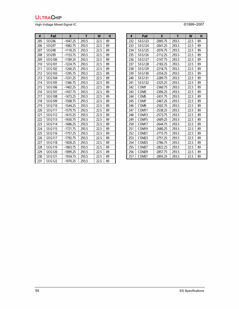
ULTRACHIP
High-Voltage Mixed-Signal IC ©1999~2007
54 ES Specifications
# Pad X Y W H 205 SEG96 -1047.25 293.5 22.5 89 206 SEG97 -1082.75 293.5 22.5 89 207 SEG98 -1118.25 293.5 22.5 89 208 SEG99 -1153.75 293.5 22.5 89 209 SEG100 -1189.25 293.5 22.5 89 210 SEG101 -1224.75 293.5 22.5 89 211 SEG102 -1260.25 293.5 22.5 89 212 SEG103 -1295.75 293.5 22.5 89 213 SEG104 -1331.25 293.5 22.5 89 214 SEG105 -1366.75 293.5 22.5 89 215 SEG106 -1402.25 293.5 22.5 89 216 SEG107 -1437.75 293.5 22.5 89 217 SEG108 -1473.25 293.5 22.5 89 218 SEG109 -1508.75 293.5 22.5 89 219 SEG110 -1544.25 293.5 22.5 89 220 SEG111 -1579.75 293.5 22.5 89 221 SEG112 -1615.25 293.5 22.5 89 222 SEG113 -1650.75 293.5 22.5 89 223 SEG114 -1686.25 293.5 22.5 89 224 SEG115 -1721.75 293.5 22.5 89 225 SEG116 -1757.25 293.5 22.5 89 226 SEG117 -1792.75 293.5 22.5 89 227 SEG118 -1828.25 293.5 22.5 89 228 SEG119 -1863.75 293.5 22.5 89 229 SEG120 -1899.25 293.5 22.5 89 230 SEG121 -1934.75 293.5 22.5 89 231 SEG122 -1970.25 293.5 22.5 89
# Pad X Y W H 232 SEG123 -2005.75 293.5 22.5 89 233 SEG124 -2041.25 293.5 22.5 89 234 SEG125 -2076.75 293.5 22.5 89 235 SEG126 -2112.25 293.5 22.5 89 236 SEG127 -2147.75 293.5 22.5 89 237 SEG128 -2183.25 293.5 22.5 89 238 SEG129 -2218.75 293.5 22.5 89 239 SEG130 -2254.25 293.5 22.5 89 240 SEG131 -2289.75 293.5 22.5 89 241 SEG132 -2325.25 293.5 22.5 89 242 COM1 -2360.75 293.5 22.5 89 243 COM3 -2396.25 293.5 22.5 89 244 COM5 -2431.75 293.5 22.5 89 245 COM7 -2467.25 293.5 22.5 89 246 COM9 -2502.75 293.5 22.5 89 247 COM11 -2538.25 293.5 22.5 89 248 COM13 -2573.75 293.5 22.5 89 249 COM15 -2609.25 293.5 22.5 89 250 COM17 -2644.75 293.5 22.5 89 251 COM19 -2680.25 293.5 22.5 89 252 COM21 -2715.75 293.5 22.5 89 253 COM23 -2751.25 293.5 22.5 89 254 COM25 -2786.75 293.5 22.5 89 255 COM27 -2822.25 293.5 22.5 89 256 COM29 -2857.75 293.5 22.5 89 257 COM31 -2893.25 293.5 22.5 89
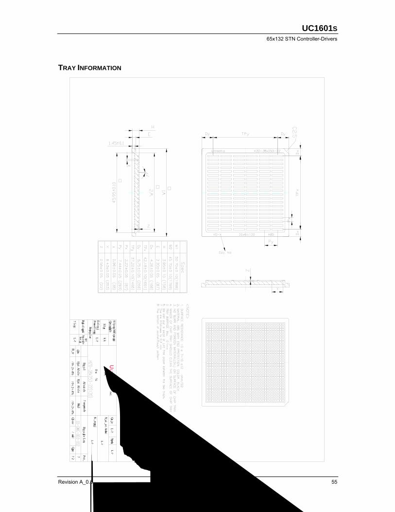
UC1601S 65x132 STN Controller-Drivers
Revision A_0.6 55
TRAY INFORMATION
N/A
Rev.
A4
A
Proj.
N/A
N/A
N/A
Drawing N
o.Approved
Material
Package C
ode
Scale
1 of 1Sheet
Joan
Size
Drawn 2 吋單面萃
mm
drawing
detail
see
N/A
12-04-06'Date
N/A
Jack Chung
By
Unit
Angle
General
Tolerance
Dimension
Roughness
Unless O
therwise
Specified
Jack Chung
Checked
ULT
RAC
HIP
INC.
晶 宏 半 導 體
12-04-06'12-04-06'
ULTRACHIP
High-Voltage Mixed-Signal IC ©1999~2007
56 ES Specifications
REVISION HISTORY Revision Contents Date of Rev.
0.1 Origin: UC1601(D) v1.1 Nov. 10, 20060.6 First release Jan. 30, 2007