Embed Size (px)
Citation preview
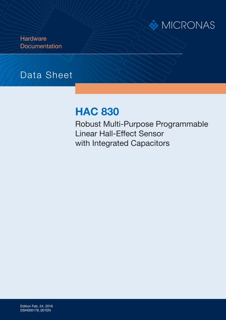
Hardware Documentation
Robust Multi-Purpose ProgrammableLinear Hall-Effect Sensorwith Integrated Capacitors
HAC 830
Hardware Documentation
DSH000178_001ENFeb. 22, 2016
Approval Document
Edition July 23, 2014AI000216_001EN
Advance Informat ion
Edition Feb. 12, 2015PD000216-002EN
Prel iminary Data Sheet
Edition Feb. 24, 2016DSH000178_001EN
Data Sheet
DATA SHEET HAC 830
Micronas Feb. 24, 2016; DSH000178_001EN 2
Copyright, Warranty, and Limitation of Liability
The information and data contained in this document are believed to be accurate andreliable. The software and proprietary information contained therein may be protectedby copyright, patent, trademark and/or other intellectual property rights of Micronas. Allrights not expressly granted remain reserved by Micronas.
Micronas assumes no liability for errors and gives no warranty representation orguarantee regarding the suitability of its products for any particular purpose due tothese specifications.
By this publication, Micronas does not assume responsibility for patent infringements orother rights of third parties which may result from its use. Commercial conditions,product availability and delivery are exclusively subject to the respective order confirma-tion.
Any information and data which may be provided in the document can and do vary indifferent applications, and actual performance may vary over time.
All operating parameters must be validated for each customer application by customers’technical experts. Any new issue of this document invalidates previous issues.Micronas reserves the right to review this document and to make changes to the docu-ment’s content at any time without obligation to notify any person or entity of suchrevision or changes. For further advice please contact us directly.
Do not use our products in life-supporting systems, military, aviation, or aerospaceapplications! Unless explicitly agreed to otherwise in writing between the parties,Micronas’ products are not designed, intended or authorized for use as components insystems intended for surgical implants into the body, or other applications intended tosupport or sustain life, or for any other application in which the failure of the productcould create a situation where personal injury or death could occur.
No part of this publication may be reproduced, photocopied, stored on a retrievalsystem or transmitted without the express written consent of Micronas.
Micronas Patents
EP0 953 848, EP 1 039 357, EP 1 575 013
Third-Party Trademarks
All other brand and product names or company names may be trademarks of theirrespective companies.

DATA SHEET HAC 830
Micronas Feb. 24, 2016; DSH000178_001EN 3
Contents, continued
Page Section Title
4 1. Introduction5 1.1. General Features5 1.2. Applications
6 2. Ordering Information6 2.1. Device-Specific Ordering Codes
8 3. Functional Description8 3.1. General Function11 3.2. Digital Signal Processing and EEPROM18 3.3. Calibration Procedure18 3.3.1. General Procedure
22 4. Specifications22 4.1. Outline Dimensions24 4.2. Soldering, Welding and Assembly24 4.3. Pin Connections and Short Descriptions25 4.4. Sensitive Area25 4.4.1. Dimension25 4.4.2. Position26 4.5. Absolute Maximum Ratings26 4.5.1. Storage and Shelf Life27 4.6. Recommended Operating Conditions28 4.7. Characteristics30 4.7.1. Definition of Sensitivity Error ES31 4.7.2. Power-On Operation32 4.8. Diagnostics and Safety Features32 4.8.1. Overvoltage and Undervoltage Detection32 4.8.2. Open-Circuit Detection33 4.8.3. Overtemperature and Short-Circuit Protection33 4.8.4. EEPROM Redundancy33 4.8.5. ADC Diagnostic
34 5. Application Notes34 5.1. Application Circuit35 5.2. Use of two HAC 830 in Parallel36 5.3. Temperature Compensation38 5.4. Ambient Temperature38 5.5. EMC and ESD
39 6. Programming39 6.1. Definition of Programming Pulses39 6.2. Definition of the Telegram42 6.3. Telegram Codes43 6.4. Number Formats44 6.5. Register Information48 6.6. Programming Information
49 7. Data Sheet History

DATA SHEET HAC 830
Robust Multi-Purpose Programmable Linear Hall-Effect Sensor with IntegratedCapacitors
1. Introduction
HAC 830 is a programmable linear Hall sensor from Micronas. It offers optimal Electro-magnetic Compatibility (EMC) protection as it integrates the HAL 830 robust multipur-pose device as well as decoupling capacitors within a single 3-pin package.
With its integrated capacitors, the HAC 830 meets the stringent ESD and EMC require-ments and eliminates the need for a PCB, thus reducing the total system size and cost.
The HAC 830 is a magnetic field sensor based on the Hall effect featuring a linear out-put. The IC can be used for angle or distance measurements when combined with arotating or moving magnet. There is no need either to add a load capacitor betweenground and the analog output or any blocking capacitor to suppress noise on the supplyline of the device.
The major characteristics like magnetic field range, sensitivity, output quiescent voltage(output voltage at B = 0 mT), and output voltage range are programmable in a non-vola-tile memory. The sensors have a ratiometric output characteristic, which means that theoutput voltage is proportional to the magnetic flux and the supply voltage.
The HAC 830 features a temperature-compensated Hall plate with spinning-current off-set compensation, an A/D converter, digital signal processing, a D/A converter with out-put driver, an EEPROM memory with redundancy and lock function for the calibrationdata, an EEPROM for customer serial number, a serial interface for programming theEEPROM, protection devices at all pins and decoupling capacitors.
The HAC 830 is programmable by modulating the supply voltage. No additional pro-gramming pin is needed. The easy programmability allows a 2-point calibration byadjusting the output voltage directly to the input signal (like mechanical angle, distance,or current). Individual adjustment of each sensor during the customer’s manufacturingprocess is possible. With this calibration procedure, the tolerances of the sensor, themagnet, and the mechanical positioning can be compensated in the final assembly. It ispossible to program several devices connected to the same supply and ground line.
In addition, the temperature compensation of the Hall IC can be fit to common magneticmaterials by programming first- and second-order temperature coefficients of the Hallsensor sensitivity. This enables operation over the full temperature range with highaccuracy.
The calculation of the individual sensor characteristics and the programming of theEEPROM memory can easily be done with a PC and the application kit from Micronas.
Micronas Feb. 24, 2016; DSH000178_001EN 4

DATA SHEET HAC 830
The sensor is designed for hostile industrial and automotive applications and isAECQ100 qualified. It operates with typically 5 V supply voltage in the ambient tem-perature range from 40 °C up to 150 °C. It is available in the very small 3-pin pack-age TO92UP-2.
1.1. General Features
– High-precision linear Hall-effect sensor with 12 bit ratiometric analog output and digital signal processing
– Multiple programmable magnetic characteristics in a non-volatile memory (EEPROM) with redundancy and lock function
– Integrated capacitors for improved Electromagnetic Compatibility (EMC) and PCB-less applications
– Operates from 40 °C up to 150 °C ambient temperature
– Operates from 4.5 V up to 5.5 V supply voltage in specification and functions up to 8.5 V
– Operates with static magnetic fields and dynamic magnetic fields up to 2 kHz
– Programmable magnetic field range from 30 mT up to 150 mT
– Open-circuit (ground and supply line break detection) with 5 k pull-up and pull-down resistor, overvoltage and undervoltage detection
– For programming an individual sensor within several sensors in parallel to the same supply voltage, a selection can be done via the output pin
– Temperature characteristics are programmable for matching common magnetic mate-rials
– Programmable clamping function
– Programming via modulation of the supply voltage
– Overvoltage- and reverse-voltage protection at all pins
– Magnetic characteristics extremely robust against mechanical stress
– Short-circuit protected push-pull output
– EMC and ESD optimized design
1.2. Applications
Due to the sensor’s versatile programming characteristics and low temperature drift, theHAC 830 is the optimal system solution for PCB-less applications such as:
– Pedal, turbo-charger, throttle and EGR systems
– Distance measurements
Micronas Feb. 24, 2016; DSH000178_001EN 5
DATA SHEET HAC 830
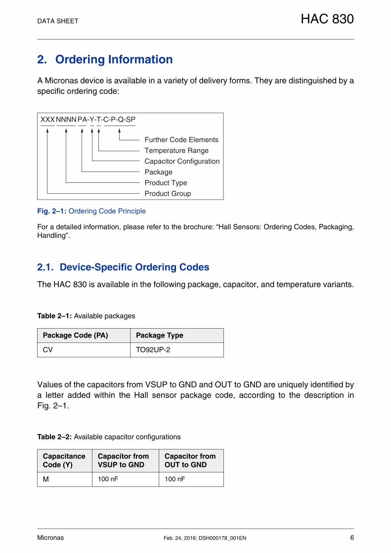
2. Ordering Information
A Micronas device is available in a variety of delivery forms. They are distinguished by aspecific ordering code:
Fig. 2–1: Ordering Code Principle
For a detailed information, please refer to the brochure: “Hall Sensors: Ordering Codes, Packaging,Handling”.
2.1. Device-Specific Ordering Codes
The HAC 830 is available in the following package, capacitor, and temperature variants.
Values of the capacitors from VSUP to GND and OUT to GND are uniquely identified bya letter added within the Hall sensor package code, according to the description inFig. 2–1.
Table 2–1: Available packages
Package Code (PA) Package Type
CV TO92UP-2
Table 2–2: Available capacitor configurations
Capacitance Code (Y)
Capacitor from VSUP to GND
Capacitor from OUT to GND
M 100 nF 100 nF
XXX NNNN PA-Y-T-C-P-Q-SP
Further Code Elements
Temperature Range
Capacitor Configuration
Package
Product Type
Product Group
Micronas Feb. 24, 2016; DSH000178_001EN 6
DATA SHEET HAC 830
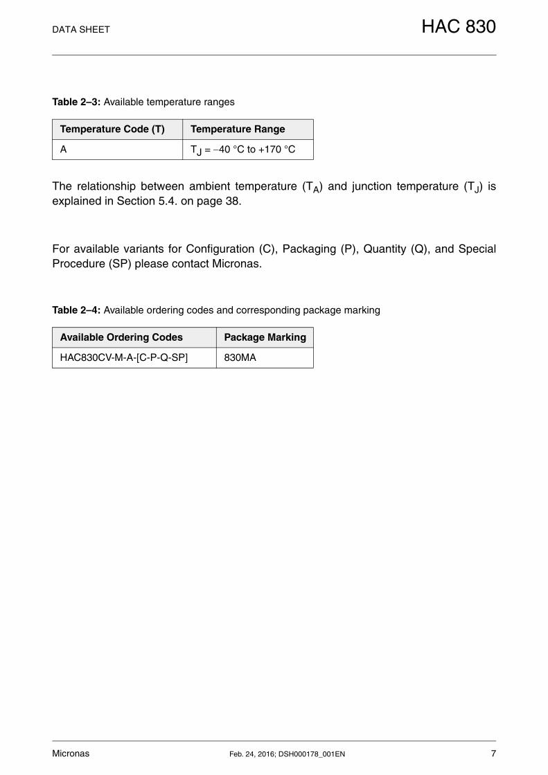
The relationship between ambient temperature (TA) and junction temperature (TJ) isexplained in Section 5.4. on page 38.
For available variants for Configuration (C), Packaging (P), Quantity (Q), and SpecialProcedure (SP) please contact Micronas.
Table 2–3: Available temperature ranges
Temperature Code (T) Temperature Range
A TJ = 40 °C to +170 °C
Table 2–4: Available ordering codes and corresponding package marking
Available Ordering Codes Package Marking
HAC830CV-M-A-[C-P-Q-SP] 830MA
Micronas Feb. 24, 2016; DSH000178_001EN 7

DATA SHEET HAC 830
3. Functional Description
3.1. General Function
The HAC 830 programmable linear Hall-Effect sensor provides an output signal propor-tional to the magnetic flux through the Hall plate and proportional to the supply voltage(ratiometric behavior) as long as the analog output mode is selected.
The external magnetic field component perpendicular to the branded side of the pack-age generates a Hall voltage. The Hall ICs are sensitive to magnetic north and southpolarity. The Hall voltage is converted to a digital value, processed in the Digital SignalProcessing Unit (DSP) according to the settings of the EEPROM registers, converted toan output signal. The function and parameters for the DSP are explained in Section 3.2.on page 11.
The setting of the LOCK register disables the programming of the EEPROM memory forall time. It also disables the reading of the memory. This register cannot be reset.
As long as the LOCK register is not set, the output characteristic can be adjusted byprogramming the EEPROM registers. The IC is addressed by modulating the supplyvoltage (see Fig. 3–1). After detecting a command, the sensor reads or writes the mem-ory and answers with a digital signal on the output pin. The output is switched off duringthe communication. Several sensors in parallel to the same supply and ground line canbe programmed individually. The selection of each sensor is done via its output pin.
The open-circuit detection function provides a defined output voltage for the analog out-put if the VSUP or GND lines are broken.
Internal temperature compensation circuitry and spinning-current offset compensationenable operation over the full temperature range with minimal changes in accuracy andhigh offset stability. The circuitry also reduces offset shifts due to mechanical stressfrom the package.
The non-volatile memory consists of redundant and non-redundant EEPROM cells. Thenon-redundant EEPROM cells are only used to store production information inside thesensor.
In addition, the sensor IC is equipped with devices for overvoltage and reverse-voltageprotection at all pins.
To improve EMC performance HAC 830 devices integrate two capacitors within thepackage, between VSUP and GND and OUT and GND respectively.
Micronas Feb. 24, 2016; DSH000178_001EN 8

DATA SHEET HAC 830
Fig. 3–1: Programming with VSUP modulation
Fig. 3–2: HAC 830 block diagram
VO
UT (
V)
5
6
7
8
VS
UP (
V)
HAC830
VSUPGND
OUT
VSUP
InternallyTemperature
Oscillator
Switched50 Digital
D/A Analog
GND
SupplyEEPROM Memory
Lock Control
Digital
StabilizedSupply andProtectionDevices
DependentBias
ProtectionDevices
Hall PlateSignalProcessing
Converter Output
LevelDetection
Output
A/DConverter
Open-Circuit, Overvoltage,UndervoltageDetection
50
Open-CircuitDetection
OUT
VSUP
CSUP
COUT
Micronas Feb. 24, 2016; DSH000178_001EN 9

DATA SHEET HAC 830
Fig. 3–3: Details of EEPROM registers and digital signal processing
Mode RegisterFilter
TC
5 bit
TCSQ
3 bit
Sensitivity
14 bit
VOQ
11 bit
Clamp Lock
1 bit
Micronas
Register2 bitRange3 bit
Clamp
EEPROM Memory
A/DConverter
DigitalFilter
Multiplier Adder Limiter D/AConverter
Digital Signal Processing
ADC-Readout Register14 bit
Lock
Control
14 bit
Digital Output
TC Range Select 2 bit
low high
Other: 8 bit
9 bit8 bit
Micronas Feb. 24, 2016; DSH000178_001EN 10
DATA SHEET HAC 830
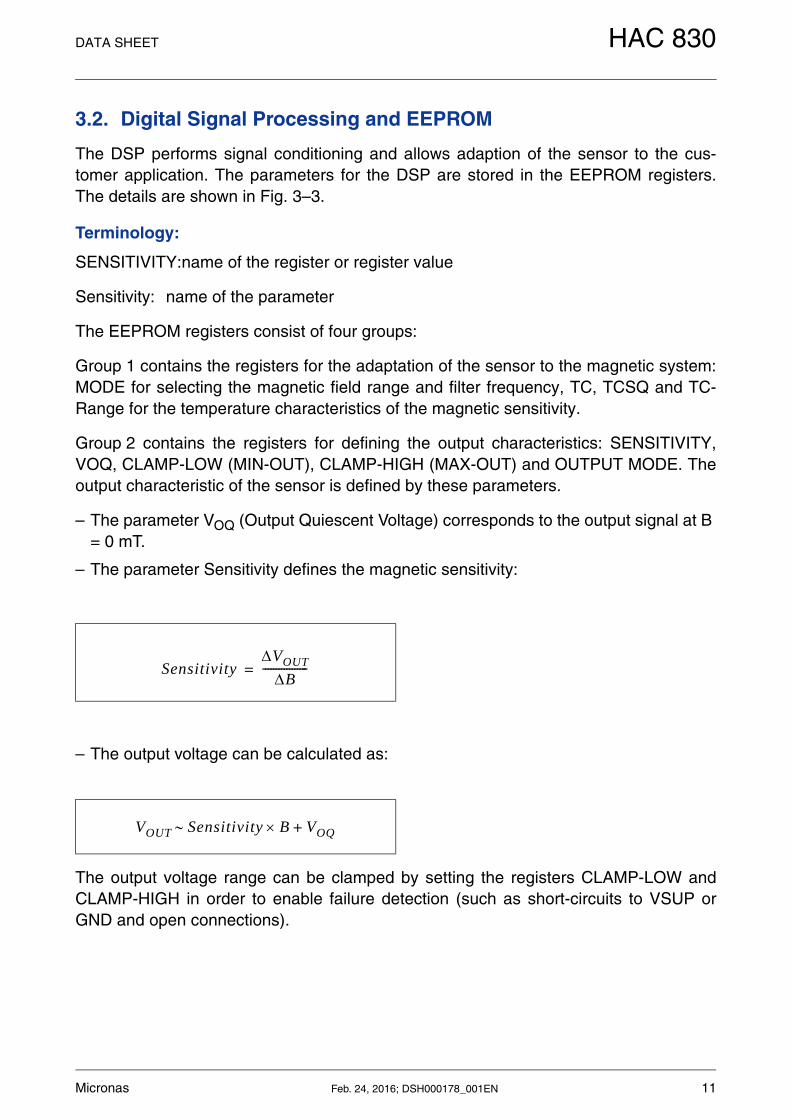
3.2. Digital Signal Processing and EEPROM
The DSP performs signal conditioning and allows adaption of the sensor to the cus-tomer application. The parameters for the DSP are stored in the EEPROM registers.The details are shown in Fig. 3–3.
Terminology:
SENSITIVITY:name of the register or register value
Sensitivity: name of the parameter
The EEPROM registers consist of four groups:
Group 1 contains the registers for the adaptation of the sensor to the magnetic system:MODE for selecting the magnetic field range and filter frequency, TC, TCSQ and TC-Range for the temperature characteristics of the magnetic sensitivity.
Group 2 contains the registers for defining the output characteristics: SENSITIVITY,VOQ, CLAMP-LOW (MIN-OUT), CLAMP-HIGH (MAX-OUT) and OUTPUT MODE. Theoutput characteristic of the sensor is defined by these parameters.
– The parameter VOQ (Output Quiescent Voltage) corresponds to the output signal at B = 0 mT.
– The parameter Sensitivity defines the magnetic sensitivity:
– The output voltage can be calculated as:
The output voltage range can be clamped by setting the registers CLAMP-LOW andCLAMP-HIGH in order to enable failure detection (such as short-circuits to VSUP orGND and open connections).
SensitivityVOUT
B-----------------=
VOUT Sensitivity B VOQ+
Micronas Feb. 24, 2016; DSH000178_001EN 11

DATA SHEET HAC 830
Group 3 contains the general purpose register GP. The GP Register can be used tostore customer information, like a serial number after manufacturing. Micronas will usethis GP REGISTER to store informations like, lot number, wafer number, x and y posi-tion of the die on the wafer, etc. This information can be read by the customer andstored in it’s own data base or it can stay in the sensor as is.
Group 4 contains the Micronas registers and LOCK for the locking of all registers. TheMICRONAS registers are programmed and locked during production. These registersare used for oscillator frequency trimming, A/D converter offset compensation, and sev-eral other special settings.
An external magnetic field generates a Hall voltage on the Hall plate. The ADC convertsthe amplified positive or negative Hall voltage (operates with magnetic north and southpoles at the branded side of the package) to a digital value. This value can be read bythe A/D-READOUT register to ensure that the suitable converter modulation isachieved. The digital signal is filtered in the internal low-pass filter and manipulatedaccording to the settings stored in the EEPROM. The digital value after signal process-ing is readable in the D/A-READOUT register. The operating range of the A/D converteris from 30 mT up to 150 mT.
During further processing, the digital signal is multiplied with the sensitivity factor,added to the quiescent output voltage level and limited according to the clamping volt-age levels. The result is converted to an analog signal and stabilized by a push-pull out-put transistor stage.
The D/A-READOUT at any given magnetic field depends on the programmed magneticfield range, the low-pass filter, TC values and CLAMP-LOW and CLAMP-HIGH. TheD/A-READOUT range is min. 0 and max. 16383.
Note During application design, it should be taken into consideration that the maximum and minimum D/A-READOUT should not violate the error band of the operational range.
Micronas Feb. 24, 2016; DSH000178_001EN 12
DATA SHEET HAC 830
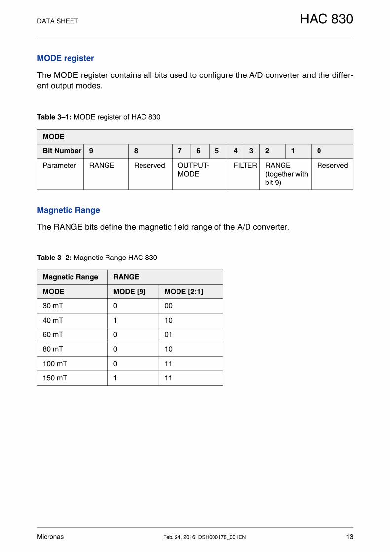
MODE register
The MODE register contains all bits used to configure the A/D converter and the differ-ent output modes.
Magnetic Range
The RANGE bits define the magnetic field range of the A/D converter.
Table 3–1: MODE register of HAC 830
MODE
Bit Number 9 8 7 6 5 4 3 2 1 0
Parameter RANGE Reserved OUTPUT-MODE
FILTER RANGE(together with bit 9)
Reserved
Table 3–2: Magnetic Range HAC 830
Magnetic Range RANGE
MODE MODE [9] MODE [2:1]
30 mT 0 00
40 mT 1 10
60 mT 0 01
80 mT 0 10
100 mT 0 11
150 mT 1 11
Micronas Feb. 24, 2016; DSH000178_001EN 13

DATA SHEET HAC 830
Filter
The FILTER bits define the 3 dB frequency of the digital low pass filter.
Output Format
The OUTPUTMODE bits define the different output modes of HAC 830.
In Analog Output mode the sensor provides an ratiometric 12 bit analog output voltagebetween 0 V and 5 V.
In Multiplex Analog Output mode the sensor transmits two analog 7-bit values, theLSB (least significant bits) and the MSB (most significant bits) of the output value sepa-rately. This enables the sensor to transmit a 14 bit signal.
– In external trigger mode the ECU can switch the output of the sensor between LSB and MSB by changing current flow direction through sensor output. In case the output is pulled up by a 10 k resistor the sensor sends the MSB. If the output is pulled down the sensor will send the LSB. Maximum refresh rate is about 500 Hz (2 ms).
– In continuous mode the sensor transmits first LSB and then MSB continuously and the ECU must listen to the data stream sent by the sensor.
In the Multiplex Analog Output mode 1 LSB is represented by a voltage level change of39 mV. In Analog Output mode with14 bit 1 LSB would be 0.31 mV.
In Burn-In Mode the signal path of the sensor’s DSP is stimulated internally withoutapplied magnetic field. In this mode the sensor provides a “saw tooth” shape output sig-nal. Shape and frequency of the saw tooth signal depend on the programming of thesensor.This mode can be used for Burn-In test in the customers production line.
Table 3–3: FILTER bits defining the 3 dB frequency
3 dB Frequency MODE [4:3]
80 Hz 00
500 Hz 10
1 kHz 11
2 kHz 01
Table 3–4: OUTPUTMODE for HAC 830
Output Format MODE [7:5]
Analog Output (12 bit) 000
Micronas Feb. 24, 2016; DSH000178_001EN 14
DATA SHEET HAC 830
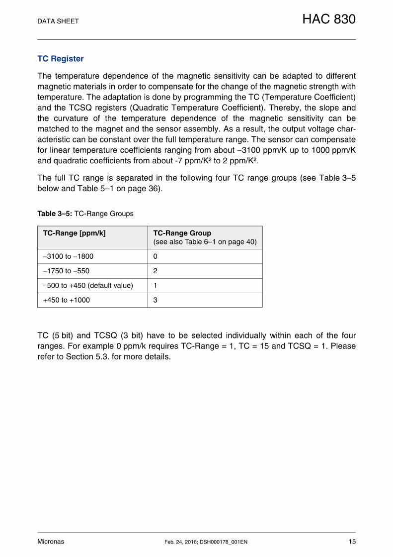
TC Register
The temperature dependence of the magnetic sensitivity can be adapted to differentmagnetic materials in order to compensate for the change of the magnetic strength withtemperature. The adaptation is done by programming the TC (Temperature Coefficient)and the TCSQ registers (Quadratic Temperature Coefficient). Thereby, the slope andthe curvature of the temperature dependence of the magnetic sensitivity can bematched to the magnet and the sensor assembly. As a result, the output voltage char-acteristic can be constant over the full temperature range. The sensor can compensatefor linear temperature coefficients ranging from about 3100 ppm/K up to 1000 ppm/Kand quadratic coefficients from about -7 ppm/K² to 2 ppm/K².
The full TC range is separated in the following four TC range groups (see Table 3–5below and Table 5–1 on page 36).
TC (5 bit) and TCSQ (3 bit) have to be selected individually within each of the fourranges. For example 0 ppm/k requires TC-Range = 1, TC = 15 and TCSQ = 1. Pleaserefer to Section 5.3. for more details.
Table 3–5: TC-Range Groups
TC-Range [ppm/k] TC-Range Group(see also Table 6–1 on page 40)
3100 to 1800 0
1750 to 550 2
500 to +450 (default value) 1
+450 to +1000 3
Micronas Feb. 24, 2016; DSH000178_001EN 15
DATA SHEET HAC 830
Sensitivity
The SENSITIVITY register contains the parameter for the multiplier in the DSP. TheSensitivity is programmable between 4 and 4. For VSUP = 5 V, the register can bechanged in steps of 0.00049.
For all calculations, the digital value from the magnetic field of the D/A converter isused. This digital information is readable from the D/A-READOUT register.
VOQ
The VOQ register contains the parameter for the adder in the DSP. VOQ is the outputsignal without external magnetic field (B = 0 mT) and programmable from VSUP (100% duty-cycle) up to VSUP (100% duty-cycle). For VSUP = 5 V, the register can bechanged in steps of 4.9 mV (0.05% duty-cycle).
Note: If VOQ is programmed to a negative value, the maximum output signal is limitedto:
Clamping Levels
The output signal range can be clamped in order to detect failures like shorts to VSUPor GND or an open circuit.
The CLAMP-LOW register contains the parameter for the lower limit. The lower clamp-ing limit is programmable between 0 V (min. duty-cycle) and VSUP/2 (50% duty-cycle).For VSUP = 5 V, the register can be changed in steps of 9.77 mV (0.195% duty-cycle).
The CLAMP-HIGH register contains the parameter for the upper limit. The upper clamp-ing voltage is programmable between 0 V (min. duty-cycle) and VSUP (max. duty-cycle).For VSUP = 5 V, in steps of 9.77 mV (0.195% duty-cycle).
VOUTmax VOQ VSUP+=
SENSITIVITYVOUT 16383
DA Readout VDD– -------------------------------------------------------------- SensINITIAL=
Micronas Feb. 24, 2016; DSH000178_001EN 16

DATA SHEET HAC 830
GP Register
This register can be used to store some information, like production date or customerserial number. Micronas will store production lot number, wafer number and x,y coordi-nates in registers GP1 to GP3. The total register contains four blocks with a length of13 bit each. The customer can read out this information and store it in his productiondata base for reference or he can store own production information instead.
Note This register is not a guarantee for traceability.
To read/write this register it is mandatory to read/write all GP register one after the other starting with GP0. In case of writing the registers it is neces-sary to first write all registers followed by one store sequence at the end. Even if only GP0 should be changed all other GP registers must first be read and the read out data must be written again to these registers.
LOCKR
By setting the 1-bit register all registers will be locked, and the sensor will no longerrespond to any supply voltage modulation. This bit is active after the first power-off andpower-on sequence after setting the LOCK bit.
Warning This register cannot be reset!
D/A-READOUT
This 14-bit register delivers the actual digital value of the applied magnetic field after thesignal processing. This register can be read out and is the basis for the calibration pro-cedure of the sensor in the system environment.
Note The MSB and LSB are reversed compared to all the other registers. Please reverse this register after readout.
Micronas Feb. 24, 2016; DSH000178_001EN 17

DATA SHEET HAC 830
3.3. Calibration Procedure
3.3.1. General Procedure
For calibration in the system environment, the application kit from Micronas is recom-mended. It contains the hardware for generation of the serial telegram for programming(Programmer Board Version 5.1) and the corresponding software (PC83x) for the inputof the register values.
For the individual calibration of each sensor in the customer application, a two pointadjustment is recommended. The calibration shall be done as follows:
Step 1: Input of the registers which are not required to be adjusted individually
The magnetic circuit, the magnetic material with its temperature characteristics, the filterfrequency, the output mode and the GP Register value are given for this application.Therefore, the values of the following registers should be identical for all sensors of thecustomer application.
– FILTER (according to the maximum signal frequency)
– RANGE(according to the maximum magnetic field at the sensor position)
– OUTPUTMODE
– TC, TCSQ and TC-RANGE(depends on the material of the magnet and the other temperature dependencies of the application)
– GP(if the customer wants to store own production information. It is not necessary to change this register)
As the clamping levels are given. They have an influence on the D/A-Readout valueand have to be set therefore after the adjustment process.
Write the appropriate settings into the HAC 830 registers.
Micronas Feb. 24, 2016; DSH000178_001EN 18
DATA SHEET HAC 830
Step 2: Initialize DSP
As the D/A-READOUT register value depends on the settings of SENSITIVITY,VOQ and CLAMP-LOW/HIGH, these registers have to be initialized with defined val-ues, first:
– VOQINITIAL = 2.5 V
– Clamp-Low = 0 V
– Clamp-High = 4.999 V
– SensINITIAL (see table 3-1.)
Step 3: Define Calibration Points
The calibration points 1 and 2 can be set inside the specified range. The correspondingvalues for VOUT1 and VOUT2 result from the application requirements.
For highest accuracy of the sensor, calibration points near the minimum and maximuminput signal are recommended. The difference of the output voltage between calibrationpoint 1 and calibration point 2 should be more than 3.5 V.
Table 3–1:
3dB Filter frequency SensINITIAL
80 Hz 0.6
500 Hz 0.39
1 kHz 0.42
2 kHz 0.83
Lowclampingvoltage VOUT1,2 Highclampingvoltage
Micronas Feb. 24, 2016; DSH000178_001EN 19

DATA SHEET HAC 830
Step 4: Calculation of VOQ and Sensitivity
Set the system to calibration point 1 and read the register D/A-READOUT. The result isthe value D/A-READOUT1.
Now, set the system to calibration point 2, read the register D/A-READOUT again, andget the value D/A-READOUT2.
With these values and the target values VOUT1 and VOUT2, for the calibration points 1and 2, respectively, the values for Sensitivity and VOQ are calculated as:
This calculation has to be done individually for each sensor.
Next, write the calculated values for Sensitivity and VOQ into the IC for adjusting thesensor. At that time it is also possible to store the application specific values for Clamp-Low and Clamp-High into the sensor’s EEPROM.The sensor is now calibrated for thecustomer application. However, the programming can be changed again and again ifnecessary.
Note For a recalibration, the calibration procedure has to be started at the begin-ning (step 1). A new initialization is necessary, as the initial values from step 1 are overwritten in step 4.
Sensitivity SensINITIALVout2 Vout1–
D/A-Readout2 D/A-Readout1– ---------------------------------------------------------------------------------
163845
---------------
=
VOQ116------ Vout2 16384
5-------------------------------------
D/A-Readout2 8192– Sensitivity 1SensINITIAL---------------------------------
–
51024------------
=
Micronas Feb. 24, 2016; DSH000178_001EN 20

DATA SHEET HAC 830
Step 5: Locking the Sensor
The last step is activating the LOCK function by programming the LOCK bit. Pleasenote that the LOCK function becomes effective after power-down and power-up of theHall IC. The sensor is now locked and does not respond to any programming or readingcommands.
Warning This register can not be reset!
Micronas Feb. 24, 2016; DSH000178_001EN 21

DATA SHEET HAC 830
4. Specifications
4.1. Outline Dimensions
Fig. 4–1:TO92UP-2: Plastic Transistor Standard UP package, 3 pinsWeight approximately 0.212 g
© Copyright 2009 Micronas GmbH, all rights reserved
DRAWING-NO.
06703.0001.4
A4, Bd, x, y= these dimensions are different for each sensor type and are specified in the data sheet.
0.36mm1.551.45
0.85 0.42
JEDEC STANDARD
ISSUE
-
ITEM NO.
-
A3UNIT A2 b c
5.605.50
5.385.28
0.600.42
1.90515.0max
ANSI
13-07-01
ISSUE DATEYY-MM-DD
D1 e E1 F2 L
0.3x45°
ZG-NO.
2.50
scale
5 mm
D1
L
e
b
F2
1
c
BdCenter ofsensitive area
E1
y
A2
A3
physical dimensions do not include moldflash.
1.200.80
F1
F1
x
ZG001100_001_02
3
P
P
solderability is guaranteed between end of pin and distance F1.
A4
2
Sn-thickness might be reduced by mechanical handling.
Micronas Feb. 24, 2016; DSH000178_001EN 22
DATA SHEET HAC 830
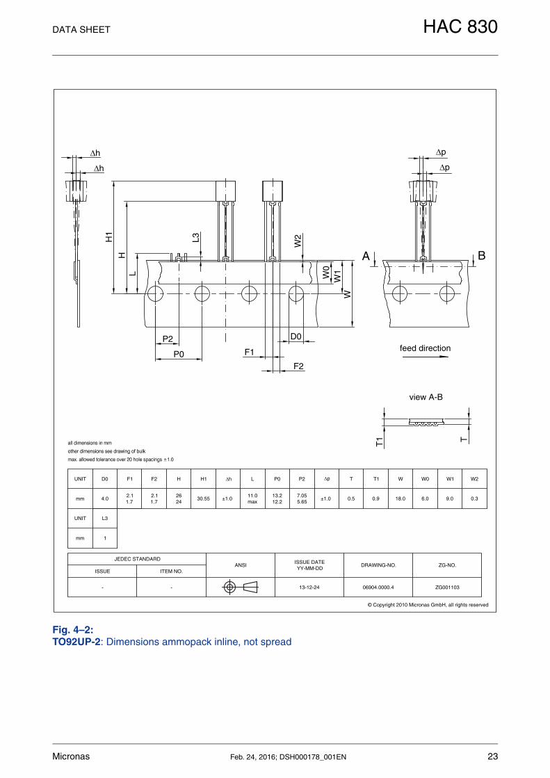
Fig. 4–2:TO92UP-2: Dimensions ammopack inline, not spread
© Copyright 2010 Micronas GmbH, all rights reserved
Δp
Δp
feed direction
T1
ITEM NO.
-
ISSUE
-
JEDEC STANDARDANSI
ISSUE DATEYY-MM-DD
13-12-24 06904.0000.4
DRAWING-NO.
view A-B
F1
HL
P0
P2W
W1
A
D0
ZG-NO.
T
B
H1
W2
W0
Δh
Δh
F2
mm
UNIT P0
13.212.2
2.11.7
4.02624
±1.011.0max
F1D0 H Δh L
7.055.65
±1.0 0.5 18.00.9 6.0
P2 Δp T T1 W W0
9.0
W1
30.55
H1
1
L3
mm
UNIT
L3
0.3
W2F2
2.11.7
ZG001103
Micronas Feb. 24, 2016; DSH000178_001EN 23

DATA SHEET HAC 830
4.2. Soldering, Welding and Assembly
Note Micronas recommends to weld the HAC 830 using resistance or laser beam welding. Reflow soldering is not permitted. Contact your Micronas sales representative for more information.
Further information related to solderability, welding, assembly, and second-level pack-aging is included in the document “Guidelines for the Assembly of Micronas Packages”. It is available on the Micronas website (http://www.micronas.com/en/service-center/downloads) or on the service portal (http://service.micronas.com).
4.3. Pin Connections and Short Descriptions
Fig. 4–3: Pin configuration
Pin No. Pin Name
Type Short Description
1 VSUP Supply Supply Voltage andProgramming Pin
2 GND GND Ground
3 OUT I/O Push-Pull Output and Selection Pin
1
2
3
VSUP
OUT
GND
CSUPCOUT
Micronas Feb. 24, 2016; DSH000178_001EN 24
DATA SHEET HAC 830
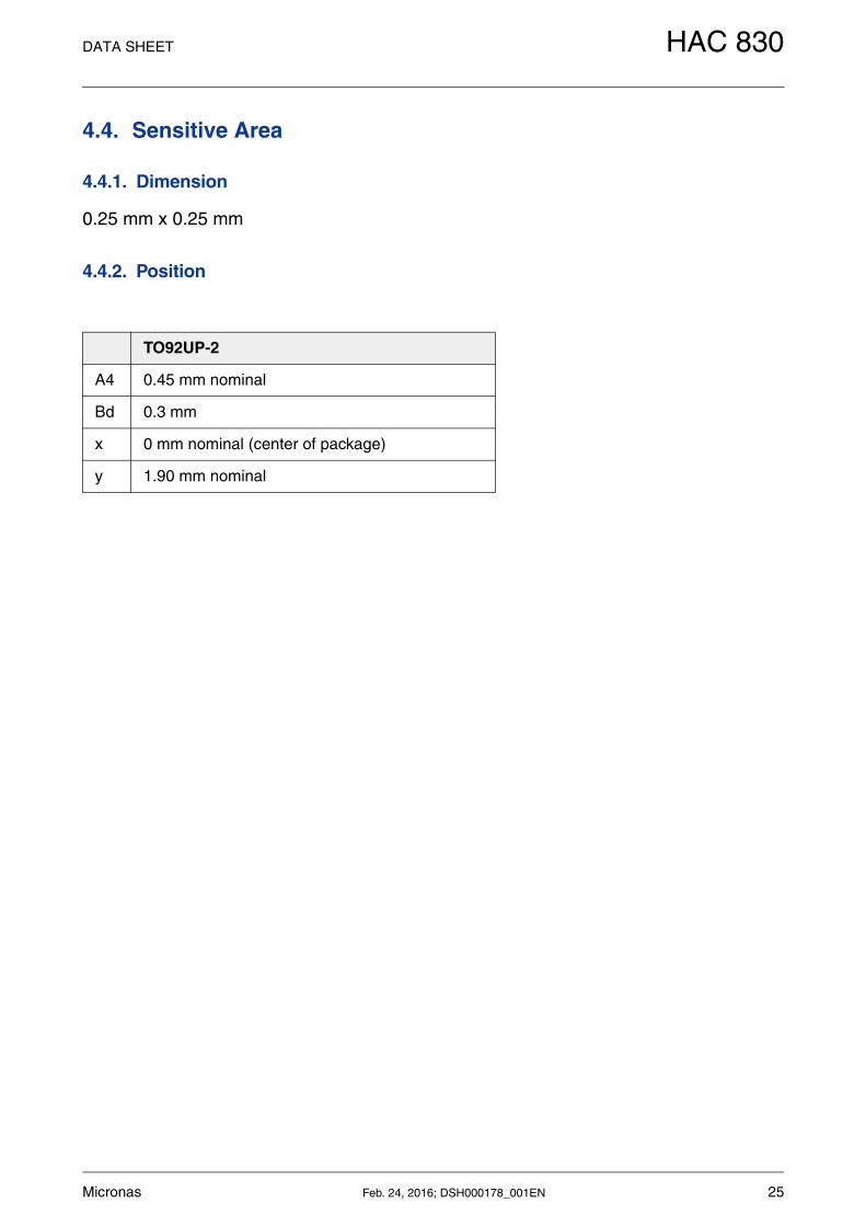
4.4. Sensitive Area
4.4.1. Dimension
0.25 mm x 0.25 mm
4.4.2. Position
TO92UP-2
A4 0.45 mm nominal
Bd 0.3 mm
x 0 mm nominal (center of package)
y 1.90 mm nominal
Micronas Feb. 24, 2016; DSH000178_001EN 25

DATA SHEET HAC 830
4.5. Absolute Maximum Ratings
Stresses beyond those listed in the “Absolute Maximum Ratings” may cause permanentdamage to the device. This is a stress rating only. Functional operation of the device atthese conditions is not implied. Exposure to absolute maximum rating conditions forextended periods will affect device reliability.
This device contains circuitry to protect the inputs and outputs against damage due tohigh static voltages or electric fields; however, it is advised that normal precautions betaken to avoid application of any voltage higher than absolute maximum-rated voltagesto this circuit.
All voltages listed are referenced to ground (GND).
4.5.1. Storage and Shelf Life
Information related to storage conditions of Micronas sensors is included in the docu-ment “Guidelines for the Assembly of Micronas Packages”. It gives recommendationslinked to moisture sensitivity level and long-term storage. It is available on the Micronas website (http://www.micronas.com/en/service-center/downloads) or on the service portal (http://service.micronas.com).
Symbol Parameter Pin No. Min. Max. Unit Condition
VSUP Supply Voltage 1 8.5 8.5 V t < 96 h3)
VSUP Supply Voltage 1 16 16 V t < 1 h3)
VOUT Output Voltage 3 5 16 V
VOUT VSUP
Excess of Output Voltage over Supply Voltage
3,1 2 V
IOUT Continuous Output Cur-rent
3 10 10 mA
tSh Output Short Circuit Dura-tion
3 10 min
VESD ESD Protection1) 13
87.5
87.5
kV
TJ Junction Temperature under bias2)
50 190 °C
1) AEC-Q100-002 (100 pF and 1.5 k)2) For 96 h - Please contact Micronas for other temperature requirements
3) No cumulated stress
Micronas Feb. 24, 2016; DSH000178_001EN 26
DATA SHEET HAC 830
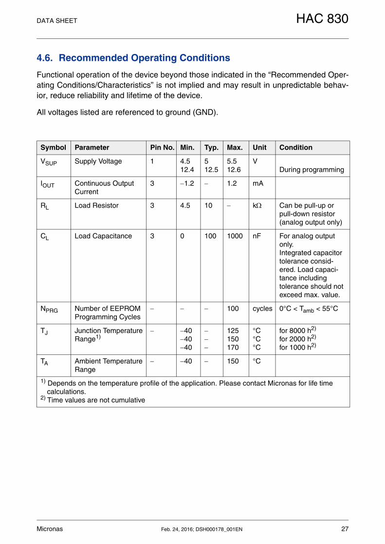
4.6. Recommended Operating Conditions
Functional operation of the device beyond those indicated in the “Recommended Oper-ating Conditions/Characteristics” is not implied and may result in unpredictable behav-ior, reduce reliability and lifetime of the device.
All voltages listed are referenced to ground (GND).
Symbol Parameter Pin No. Min. Typ. Max. Unit Condition
VSUP Supply Voltage 1 4.512.4
512.5
5.512.6
VDuring programming
IOUT Continuous Output Current
3 1.2 1.2 mA
RL Load Resistor 3 4.5 10 k Can be pull-up or pull-down resistor (analog output only)
CL Load Capacitance 3 0 100 1000 nF For analog output only.Integrated capacitor tolerance consid-ered. Load capaci-tance including tolerance should not exceed max. value.
NPRG Number of EEPROMProgramming Cycles
100 cycles 0°C < Tamb < 55°C
TJ Junction Temperature Range1)
404040
125150170
°C°C°C
for 8000 h2) for 2000 h2)
for 1000 h2)
TA Ambient Temperature Range
40 150 °C
1) Depends on the temperature profile of the application. Please contact Micronas for life timecalculations.
2) Time values are not cumulative
Micronas Feb. 24, 2016; DSH000178_001EN 27

DATA SHEET HAC 830
4.7. Characteristics
at TJ = 40 °C to +170 °C, VSUP = 4.5 V to 5.5 V, GND = 0 V after programming and locking, at Rec-ommended Operation Conditions if not otherwise specified in the column “Conditions”.Typical Characteristics for TJ = 25 °C and VSUP = 5 V.
Symbol Parameter Pin No.
Min. Typ. Max. Unit Conditions
ISUP Supply Current over Temperature Range
1 5 7 10 mA
CSUP Integrated Supply Capaci-tor Tolerance
1 10 +10 % @ 25 °C and VSUP=5 VVariation is given relative to nominal value. For typical val-ues see Table 2–2 on page 6COUT Integrated Output Capacitor
Tolerance3
ES Error in Magnetic Sensitivity over Temperature Range5)
3 4 0 4 % VSUP = 5 V; 60 mT range, 3 dB frequency = 500 Hz, TC & TCSQ for linearized temper-ature coefficients(see Section 4.7.1. on page 30)
Analog Output
Resolution 3 12 bit ratiometric to VSUP 1)
DNL Differential Non-Linearity of D/A converter2)
3 2.0 0 2.0 LSB Only @ 25 °C ambient tem-perature
INL Non-Linearity of Output Volt-age over Temperature
3 0.5 0 0.5 % % of supply voltage3)
For VOUT = 0.35 V...4.65 V;VSUP = 5 V, Sensitivity 0.95
ER Ratiometric Error of Output over Temperature (Error in VOUT / VSUP)
3 0.25 0 0.25 % VOUT1 VOUT2> 2 Vduring calibration procedure
VOffset Offset Drift over Tempera-ture RangeVOUT(B=0 mT)25°C VOUT(B=0 mT)max
5)
3 0.6 0.25 0.6 % VSU
P
VSUP = 5 V; 60 mT range,3 dB frequency = 500 Hz, TC = 15, TCSQ = 1, TC-Range = 10.65 < sensitivity < 0.65
1) Output DAC full scale = 5 V ratiometric, Output DAC offset = 0 V, Output DAC LSB = VSUP/40962) Only tested at 25°C. The specified values are test limits only. Overmolding and packaging might influence
this parameter3) If more than 50% of the selected magnetic field range is used (Sensitivity 0.5) and the temperature com-
pensation is suitable. INL = VOUT VOUTLSF=Least Square Fit Line voltage based on VOUT measurements at a fixed temperature.
4)Signal Band Area with full accuracy is located between VOUTL and VOUTH. The sensor accuracy is reduced below VOUTL and above VOUTH
5) Tambient = 150 °C
Micronas Feb. 24, 2016; DSH000178_001EN 28

DATA SHEET HAC 830
VOUTCL Accuracy of Output Voltage at Clamping Low Voltage over Temperature Range
3 15 0 15 mV RL = 5 k, VSUP = 5 VSpec values are derived from resolutions of the registers Clamp-Low/Clamp-High and the parameter VoffsetVOUTCH Accuracy of Output Voltage
at Clamping High Voltage over Temperature Range
3 15 0 15 mV
VOUTH Upper Limit of Signal Band4) 3 4.65 4.8 V VSUP = 5 V,1 mA IOUT 1 mA
VOUTL Lower Limit of Signal Band4) 3 0.2 0.35 V VSUP = 5 V, 1 mA IOUT 1 mA
ROUT Output Resistance over Recommended Operating Range
3 1 10 VOUTLmax VOUT VOUTHmin
tr(O) Step Response Time of Output6)
3 30.90.60.4
131.20.80.5
ms 3 dB Filter frequency=80 Hz3 dB Filter frequency=500 Hz3 dB Filter frequency=1 kHz3 dB Filter frequency=2 kHztime from 10% to 90% of final output voltage for a steplike signal Bstep from 0 mT to Bmax
tPOD Power-Up Time (Time to reach stable Output Voltage)
1.5 1.7 1.9 ms 90% of VOUT
BW Small Signal Bandwidth (3 dB)
3 2 kHz BAC < 10 mT;3 dB Filter frequency=2 kHz
VOUTn Noise Output VoltageRMS 3 1 5 mV magnetic range=60 mT3 dB Filter frequency=500 HzSensitivity 0.7 6)
DACGE D/A-Converter Glitch Energy
3 40 nVs 7)
TO92UP-2 Package
Rthja
Rthjc
Thermal Resistance
junction to air
junction to case
1981465338
K/W Measured with a 1s0p boardMeasured with a 1s1p boardMeasured with a 1s0p boardMeasured with a 1s1p board
4) Signal Band Area with full accuracy is located between VOUTL and VOUTH. The sensor accuracyis reduced below VOUTL and above VOUTH
6) Guaranteed by design7) The energy of the impulse injected into the analog output when the code in the D/A-Converter
register changes state. This energy is normally specified as the area of the glitch in nVs.
Symbol Parameter Pin No.
Min. Typ. Max. Unit Conditions
Micronas Feb. 24, 2016; DSH000178_001EN 29
DATA SHEET HAC 830
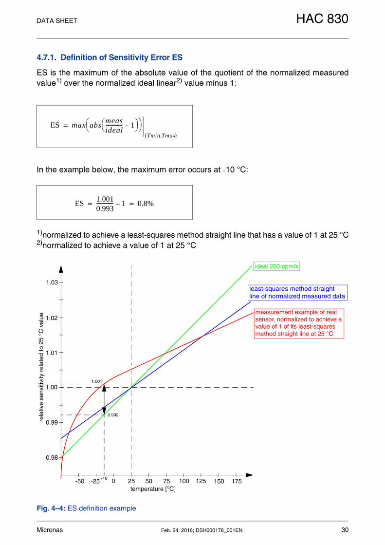
4.7.1. Definition of Sensitivity Error ES
ES is the maximum of the absolute value of the quotient of the normalized measuredvalue1) over the normalized ideal linear2) value minus 1:
In the example below, the maximum error occurs at 10 °C:
1)normalized to achieve a least-squares method straight line that has a value of 1 at 25 °C2)normalized to achieve a value of 1 at 25 °C
Fig. 4–4: ES definition example
ES max absmeasideal------------- 1–
Tmin Tmax{ , }
=
ES1.0010.993------------- 1– 0.8%= =
50 75 100 125 150 175250-25-50
0.98
0.99
1.00
1.01
1.02
1.03
-10
0.992
1.001
temperature [°C]
rela
tive
sens
itivi
ty r
elat
ed to
25
°C v
alue
ideal 200 ppm/k
measurement example of realsensor, normalized to achieve avalue of 1 of its least-squaresmethod straight line at 25 °C
least-squares method straight line of normalized measured data
Micronas Feb. 24, 2016; DSH000178_001EN 30
DATA SHEET HAC 830
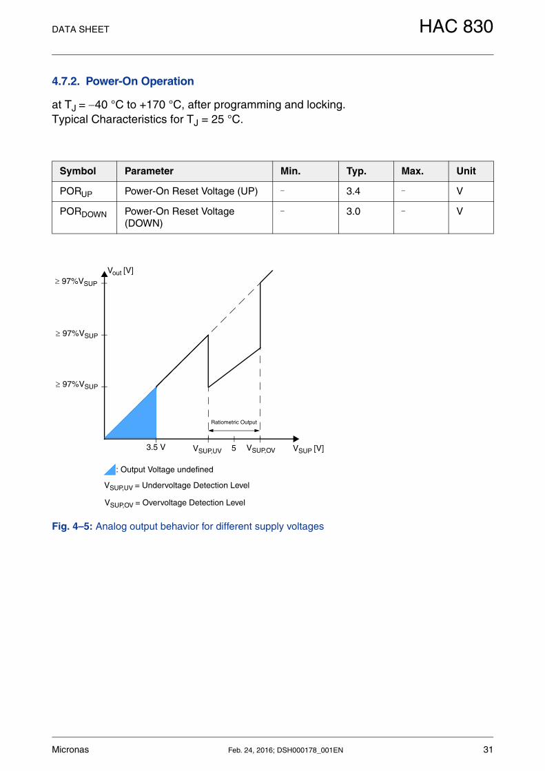
4.7.2. Power-On Operation
at TJ = 40 °C to +170 °C, after programming and locking. Typical Characteristics for TJ = 25 °C.
Fig. 4–5: Analog output behavior for different supply voltages
Symbol Parameter Min. Typ. Max. Unit
PORUP Power-On Reset Voltage (UP) 3.4 V
PORDOWN Power-On Reset Voltage (DOWN)
3.0 V
VSUP,UV 5 VSUP,OV VSUP [V]
Vout [V]
97%VSUP
97%VSUP
: Output Voltage undefined
3.5 V
97%VSUP
Ratiometric Output
VSUP,UV = Undervoltage Detection Level
VSUP,OV = Overvoltage Detection Level
Micronas Feb. 24, 2016; DSH000178_001EN 31

DATA SHEET HAC 830
4.8. Diagnostics and Safety Features
4.8.1. Overvoltage and Undervoltage Detection
at TJ = 40 °C to +170 °C, Typical Characteristics for TJ = 25 °C, after programming and locking
Note The over- and undervoltage detection is activated only after locking the sensor!
4.8.2. Open-Circuit Detection
at TJ = 40 °C to +170 °C, Typical Characteristics for TJ = 25 °C, after locking the sensor.
Symbol Parameter Pin No.
Min. Typ. Max. Unit Test Conditions
VSUP,UV Undervoltage detec-tion level
1 4.2 4.5 V 1)
VSUP,OV Overvoltage detec-tion level
1 8.5 8.9 10.0 V 1)
1) If the supply voltage drops below VSUP,UV or rises above VSUP,OV, the output voltage is switched to VSUP (97% of VSUP at RL = 10 k to GND).
Symbol Parameter Pin No. Min. Typ. Max. Unit Comment
VOUT Output Voltage at open VSUP line
3 0 0 0.15 V VSUP = 5 VRL = 10 kto 200k
0 0 0.2 V VSUP = 5 V5 kRL < 10 k
0 0 0.25 V VSUP = 5 V4.5 kRL < 10 k1)
VOUT Output Voltage at open GND line
3 4.85 4.9 5.0 V VSUP = 5 VRL = 10 kto 200k
4.8 4.9 5.0 V VSUP = 5 V5 kRL < 10 k
4.75 4.9 5.0 V VSUP = 5 V4.5 kRL < 10 k1)
1) not tested
Micronas Feb. 24, 2016; DSH000178_001EN 32
DATA SHEET HAC 830
4.8.3. Overtemperature and Short-Circuit Protection
If overtemperature TJ>180 °C or a short-circuit occurs, the output will go into tri-statecondition.
4.8.4. EEPROM Redundancy
The non-volatile memory uses the Micronas Fail Safe Redundant Cell technology wellproven in automotive applications.
4.8.5. ADC Diagnostic
The A/D-READOUT register can be used to avoid under/overrange effects in the A/Dconverter.
Micronas Feb. 24, 2016; DSH000178_001EN 33
DATA SHEET HAC 830
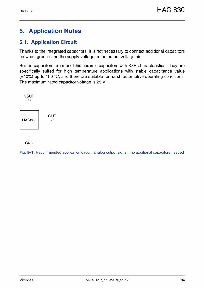
5. Application Notes
5.1. Application Circuit
Thanks to the integrated capacitors, it is not necessary to connect additional capacitorsbetween ground and the supply voltage or the output voltage pin.
Built-in capacitors are monolithic ceramic capacitors with X8R characteristics. They arespecifically suited for high temperature applications with stable capacitance value(±10%) up to 150 °C, and therefore suitable for harsh automotive operating conditions.The maximum rated capacitor voltage is 25 V.
Fig. 5–1: Recommended application circuit (analog output signal), no additional capacitors needed
OUT
VSUP
GND
HAC830
Micronas Feb. 24, 2016; DSH000178_001EN 34

DATA SHEET HAC 830
5.2. Use of two HAC 830 in Parallel
Two different HAC 830 sensors which are operated in parallel to the same supply andground line can be programmed individually. In order to select the IC which should beprogrammed, both Hall ICs are inactivated by the “Deactivate” command on the com-mon supply line. Then, the appropriate IC is activated by an “Activate” pulse on its out-put. Only the activated sensor will react to all following read, write, and program com-mands. If the second IC has to be programmed, the “Deactivate” command is sentagain, and the second IC can be selected.
Note The multi-programming of two sensors requires a 10 k pull-down resistor on the sensors’ output pins.
Fig. 5–2: Recommended application circuit (parallel operation of two HAC 830), no additional capacitors needed
HAC830
GND
HAC830Sensor A Sensor B
VSUP
OUT B & Select B
OUT A & Select A
Micronas Feb. 24, 2016; DSH000178_001EN 35
DATA SHEET HAC 830
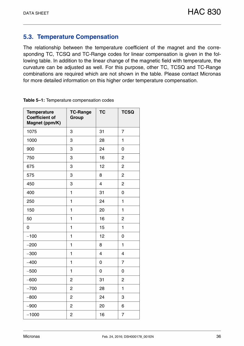
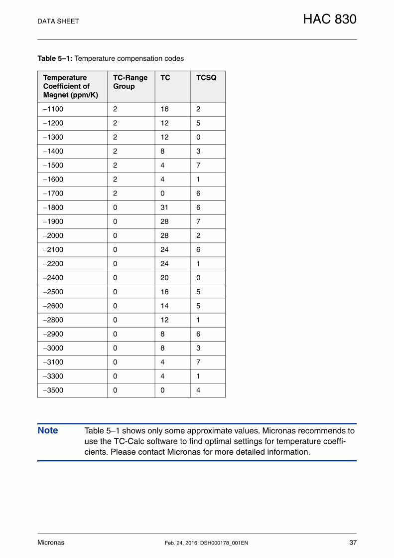
5.3. Temperature Compensation
The relationship between the temperature coefficient of the magnet and the corre-sponding TC, TCSQ and TC-Range codes for linear compensation is given in the fol-lowing table. In addition to the linear change of the magnetic field with temperature, thecurvature can be adjusted as well. For this purpose, other TC, TCSQ and TC-Rangecombinations are required which are not shown in the table. Please contact Micronasfor more detailed information on this higher order temperature compensation.
Table 5–1: Temperature compensation codes
Temperature Coefficient of Magnet (ppm/K)
TC-Range Group
TC TCSQ
1075 3 31 7
1000 3 28 1
900 3 24 0
750 3 16 2
675 3 12 2
575 3 8 2
450 3 4 2
400 1 31 0
250 1 24 1
150 1 20 1
50 1 16 2
0 1 15 1
100 1 12 0
200 1 8 1
300 1 4 4
400 1 0 7
500 1 0 0
600 2 31 2
700 2 28 1
800 2 24 3
900 2 20 6
1000 2 16 7
Micronas Feb. 24, 2016; DSH000178_001EN 36
DATA SHEET HAC 830
Note Table 5–1 shows only some approximate values. Micronas recommends to use the TC-Calc software to find optimal settings for temperature coeffi-cients. Please contact Micronas for more detailed information.
1100 2 16 2
1200 2 12 5
1300 2 12 0
1400 2 8 3
1500 2 4 7
1600 2 4 1
1700 2 0 6
1800 0 31 6
1900 0 28 7
2000 0 28 2
2100 0 24 6
2200 0 24 1
2400 0 20 0
2500 0 16 5
2600 0 14 5
2800 0 12 1
2900 0 8 6
3000 0 8 3
3100 0 4 7
3300 0 4 1
3500 0 0 4
Table 5–1: Temperature compensation codes
Temperature Coefficient of Magnet (ppm/K)
TC-Range Group
TC TCSQ
Micronas Feb. 24, 2016; DSH000178_001EN 37

DATA SHEET HAC 830
5.4. Ambient Temperature
Due to the internal power dissipation, the temperature on the silicon chip (junction tem-perature TJ) is higher than the temperature outside the package (ambient temperatureTA).
TJ = TA + T
At static conditions and continuous operation, the following equation applies:
T = ISUP * VSUP * RthjX
The X represents junction-to-air or junction-to-case.
In order to estimate the temperature difference T between the junction and the respec-tive reference (e.g. air, case, or solder point) use the max. parameters for ISUP, RthX,and the max. value for VSUP from the application.
The following example shows the result for junction-to -air conditions. VSUP = 5.5 V,Rthja = 250 K/W and ISUP = 10 mA the temperature difference T = 13.75 K.
The junction temperature TJ is specified. The maximum ambient temperature TAmax canbe estimated as:
TAmax = TJmax T
5.5. EMC and ESD
Please contact Micronas for the detailed investigation reports with the EMC andESD results.
Micronas Feb. 24, 2016; DSH000178_001EN 38
DATA SHEET HAC 830
6. Programming
6.1. Definition of Programming Pulses
The sensor is addressed by modulating a serial telegram on the supply voltage. Thesensor answers with a serial telegram on the output pin.
The bits in the serial telegram have a different bit time for the VSUP-line and the output.The bit time for the VSUP-line is defined through the length of the Sync Bit at the begin-ning of each telegram. The bit time for the output is defined through the AcknowledgeBit.
A logical “0” is coded as no voltage change within the bit time. A logical “1” is coded asa voltage change between 50% and 80% of the bit time. After each bit, a voltagechange occurs.
6.2. Definition of the Telegram
Each telegram starts with the Sync Bit (logical 0), 3 bits for the Command (COM), theCommand Parity Bit (CP), 4 bits for the Address (ADR), and the Address Parity Bit (AP).
There are 4 kinds of telegrams:
– Write a register (see Fig. )After the AP Bit, follow 14 Data Bits (DAT) and the Data Parity Bit (DP). If the telegramis valid and the command has been processed, the sensor answers with an Acknowl-edge Bit (logical 0) on the output.
– Read a register (see Fig. 6–3)After evaluating this command, the sensor answers with the Acknowledge Bit, 14Data Bits, and the Data Parity Bit on the output.
– Programming the EEPROM cells (see Fig. 6–4)After evaluating this command, the sensor answers with the Acknowledge Bit. Afterthe delay time tw, the supply voltage rises up to the programming voltage.
– Activate a sensor (see Fig. 6–4)If more than one sensor is connected to the supply line, selection can be done by firstdeactivating all sensors. The output of all sensors have to be pulled to ground. Withan Activate pulse on the appropriate output pin, an individual sensor can be selected.All following commands will only be accepted from the activated sensor.
Micronas Feb. 24, 2016; DSH000178_001EN 39
DATA SHEET HAC 830
Fig. 6–1: Definition of logical 0 and 1 bit
Table 6–1: Telegram parameters
Symbol Parameter Pin Min. Typ. Max. Unit Remarks
VSUPL Supply Voltage for Low Levelduring Programming
1 5 5.6 6 V
VSUPH Supply Voltage for High Levelduring Programming
1 6.8 8.0 8.5 V
tr Rise time 1 0.05 ms see Fig. 6–1 on page 40
tf Fall time 1 0.05 ms see Fig. 6–1 on page 40
tp0 Bit time on VSUP 1 1.7 1.75 1.9 ms tp0 is defined through the Sync Bit
tpOUT Bit time on output pin 3 2 3 4 ms tpOUT is defined through the Acknowledge Bit
tp1 Duty-Cycle Change for logical 1 1, 3
50 65 80 % % of tp0 or tpOUT
VSUP-
PROG
Supply Voltage for Programming the EEPROM
1 12.4 12.5 12.6 V
tPROG Programming Time for EEPROM 1 95 100 105 ms
trp Rise time of programming voltage 1 0.2 0.5 1 ms see Fig. 6–1 on page 40
tfp Fall time of programming voltage 1 0 1 ms see Fig. 6–1 on page 40
tw Delay time of programming volt-age after Acknowledge
1 0.5 0.7 1 ms
Vact Voltage for an Activate pulse 3 3 4 5 V
tact Duration of an Activate pulse 3 0.05 0.1 0.2 ms
Vout,deact
Output voltage after deactivate command
3 0 0.1 0.2 V
tr tf
tp0 tp0logical 0
VSUPH
VSUPL
or
tp0logical 1
VSUPH
VSUPL
ortp0
tp1
tp1
Micronas Feb. 24, 2016; DSH000178_001EN 40

DATA SHEET HAC 830
Fig. 6–2: Telegram for coding a Write command
Fig. 6–3: Telegram for coding a Read command
Fig. 6–4: Telegram for coding the EEPROM programming
Fig. 6–5: Activate pulse
Sync COM CP ADR AP DAT DP
Acknowledge
VSUP
VOUT
WRITE
Sync COM CP ADR AP
DAT DPAcknowledge
VSUP
VOUT
READ
Sync COM CP ADR AP
tPROG
Acknowledge
VSUP
VOUT
ERASE, PROM, and LOCK
trp tfp
tw
VSUPPROG
tACT
VOUT
tr tfVACT
Micronas Feb. 24, 2016; DSH000178_001EN 41
DATA SHEET HAC 830
6.3. Telegram Codes
Sync Bit
Each telegram starts with the Sync Bit. This logical “0” pulse defines the exact timing fortp0.
Command Bits (COM)
The Command code contains 3 bits and is a binary number. Table 6–2 shows the avail-able commands and the corresponding codes for the HAC 830.
Command Parity Bit (CP)
This parity bit is “1” if the number of zeros within the 3 Command Bits is uneven. Theparity bit is “0”, if the number of zeros is even.
Address Bits (ADR)
The Address code contains 4 bits and is a binary number. Table 6–3 shows the avail-able addresses for the HAC 830 registers.
Address Parity Bit (AP)
This parity bit is “1” if the number of zeros within the 4 Address bits is uneven. The par-ity bit is “0” if the number of zeros is even.
Data Bits (DAT)
The 14 Data Bits contain the register information.
The registers use different number formats for the Data Bits. These formats areexplained in Section 6.4.
In the Write command, the last bits are valid. If, for example, the TC register (10 bits) iswritten, only the last 10 bits are valid.
In the Read command, the first bits are valid. If, for example, the TC register (10 bits) isread, only the first 10 bits are valid.
Data Parity Bit (DP)
This parity bit is “1” if the number of zeros within the binary number is even. The paritybit is “0” if the number of zeros is uneven.
Micronas Feb. 24, 2016; DSH000178_001EN 42

DATA SHEET HAC 830
Acknowledge
After each telegram, the output answers with the Acknowledge signal. This logical “0”pulse defines the exact timing for tpOUT.
6.4. Number Formats
Binary number:
The most significant bit is given as first, the least significant bit as last digit.
Example: 101001 represents 41 decimal.
Signed binary number:
The first digit represents the sign of the following binary number (1 for negative, 0 forpositive sign).
Example: 0101001 represents +41 decimal1101001 represents 41 decimal
Two’s-complement number:
The first digit of positive numbers is “0”, the rest of the number is a binary number. Neg-ative numbers start with “1”. In order to calculate the absolute value of the number, cal-culate the complement of the remaining digits and add “1”.
Example: 0101001 represents +41 decimal1010111 represents 41 decimal
Table 6–2: Available commands
Command Code Explanation
READ 2 read a register
WRITE 3 write a register
PROM 4 program all non-volatile registers
ERASE 5 erase all non-volatile registers
Micronas Feb. 24, 2016; DSH000178_001EN 43
DATA SHEET HAC 830
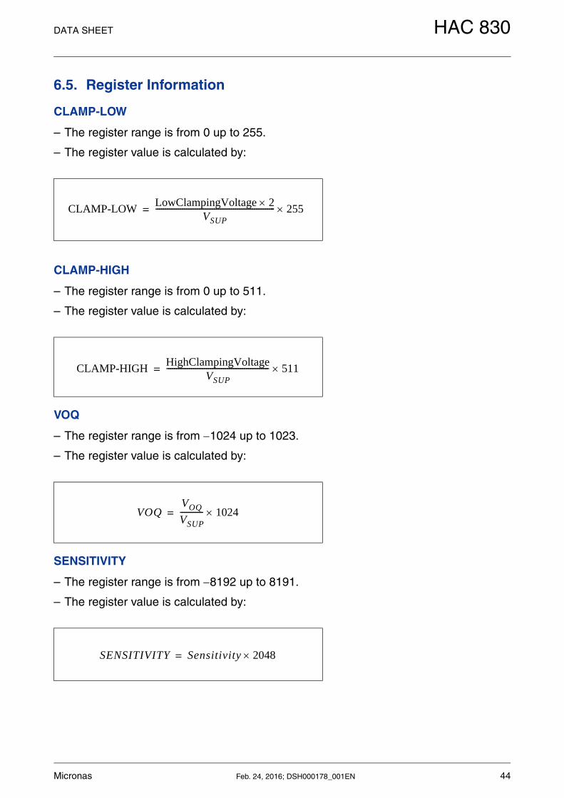
6.5. Register Information
CLAMP-LOW
– The register range is from 0 up to 255.
– The register value is calculated by:
CLAMP-HIGH
– The register range is from 0 up to 511.
– The register value is calculated by:
VOQ
– The register range is from 1024 up to 1023.
– The register value is calculated by:
SENSITIVITY
– The register range is from 8192 up to 8191.
– The register value is calculated by:
CLAMP-LOWLowClampingVoltage 2
VSUP--------------------------------------------------------------- 255=
CLAMP-HIGHHighClampingVoltage
VSUP------------------------------------------------------ 511=
VOQVOQ
VSUP------------ 1024=
SENSITIVITY Sensitivity 2048=
Micronas Feb. 24, 2016; DSH000178_001EN 44
DATA SHEET HAC 830
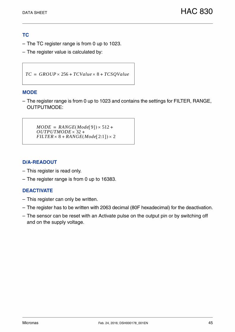
TC
– The TC register range is from 0 up to 1023.
– The register value is calculated by:
MODE
– The register range is from 0 up to 1023 and contains the settings for FILTER, RANGE, OUTPUTMODE:
D/A-READOUT
– This register is read only.
– The register range is from 0 up to 16383.
DEACTIVATE
– This register can only be written.
– The register has to be written with 2063 decimal (80F hexadecimal) for the deactivation.
– The sensor can be reset with an Activate pulse on the output pin or by switching off and on the supply voltage.
TC GROUP 256 TCValue 8 TCSQValue++=
MODE RANGE Mode 9 512OUTPUTMODE
+32
FILTER 8 RANGE Mode 2:1 2++
=
Micronas Feb. 24, 2016; DSH000178_001EN 45
DATA SHEET HAC 830
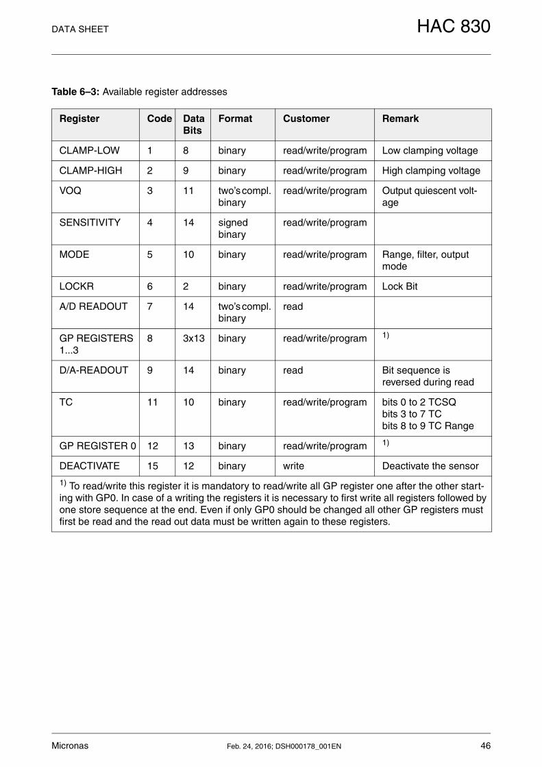
Table 6–3: Available register addresses
Register Code Data Bits
Format Customer Remark
CLAMP-LOW 1 8 binary read/write/program Low clamping voltage
CLAMP-HIGH 2 9 binary read/write/program High clamping voltage
VOQ 3 11 two’s compl. binary
read/write/program Output quiescent volt-age
SENSITIVITY 4 14 signed binary
read/write/program
MODE 5 10 binary read/write/program Range, filter, output mode
LOCKR 6 2 binary read/write/program Lock Bit
A/D READOUT 7 14 two’s compl. binary
read
GP REGISTERS 1...3
8 3x13 binary read/write/program 1)
D/A-READOUT 9 14 binary read Bit sequence is reversed during read
TC 11 10 binary read/write/program bits 0 to 2 TCSQbits 3 to 7 TCbits 8 to 9 TC Range
GP REGISTER 0 12 13 binary read/write/program 1)
DEACTIVATE 15 12 binary write Deactivate the sensor
1) To read/write this register it is mandatory to read/write all GP register one after the other start-ing with GP0. In case of a writing the registers it is necessary to first write all registers followed by one store sequence at the end. Even if only GP0 should be changed all other GP registers must first be read and the read out data must be written again to these registers.
Micronas Feb. 24, 2016; DSH000178_001EN 46
DATA SHEET HAC 830
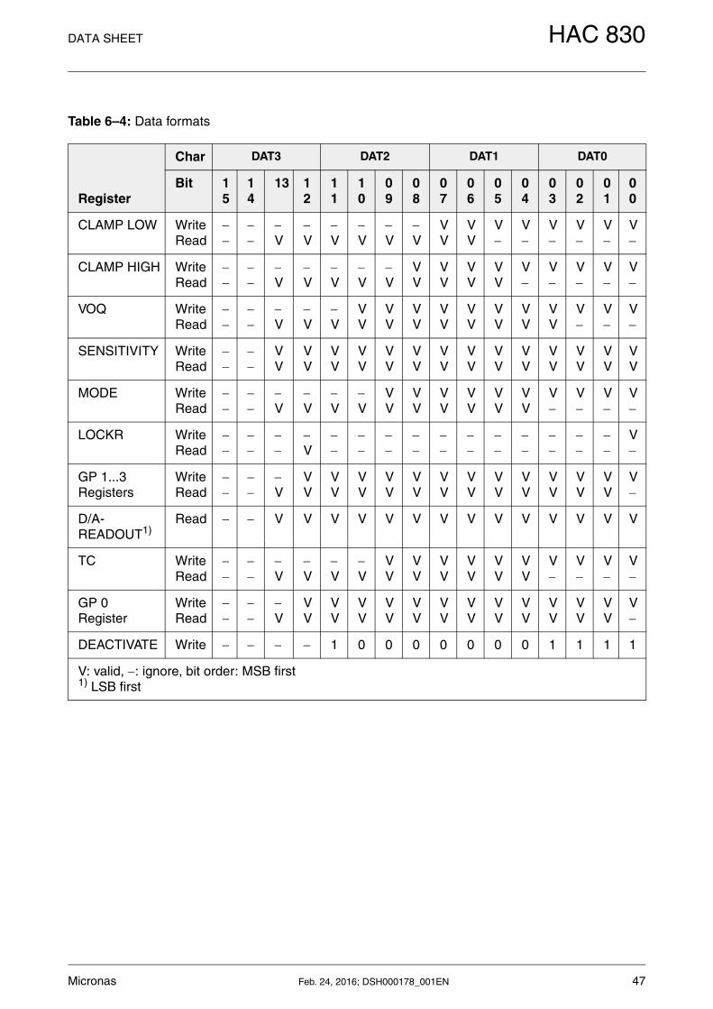
Table 6–4: Data formats
Register
Char DAT3 DAT2 DAT1 DAT0
Bit 15
14
13 12
11
10
09
08
07
06
05
04
03
02
01
00
CLAMP LOW WriteRead
V
V
V
V
V
V
VV
VV
V
V
V
V
V
V
CLAMP HIGH WriteRead
V
V
V
V
V
VV
VV
VV
VV
V
V
V
V
V
VOQ WriteRead
V
V
V
VV
VV
VV
VV
VV
VV
VV
VV
V
V
V
SENSITIVITY WriteRead
VV
VV
VV
VV
VV
VV
VV
VV
VV
VV
VV
VV
VV
VV
MODE WriteRead
V
V
V
V
VV
VV
VV
VV
VV
VV
V
V
V
V
LOCKR WriteRead
V
V
GP 1...3Registers
WriteRead
V
VV
VV
VV
VV
VV
VV
VV
VV
VV
VV
VV
VV
V
D/A-READOUT1)
Read V V V V V V V V V V V V V V
TC WriteRead
V
V
V
V
VV
VV
VV
VV
VV
VV
V
V
V
V
GP 0Register
WriteRead
V
VV
VV
VV
VV
VV
VV
VV
VV
VV
VV
VV
VV
V
DEACTIVATE Write 1 0 0 0 0 0 0 0 1 1 1 1
V: valid, : ignore, bit order: MSB first1) LSB first
Micronas Feb. 24, 2016; DSH000178_001EN 47

DATA SHEET HAC 830
6.6. Programming Information
If the content of any register (except the lock registers) is to be changed, the desiredvalue must first be written into the corresponding RAM register. Before reading out theRAM register again, the register value must be permanently stored in the EEPROM.
Permanently storing a value in the EEPROM is done by first sending an ERASE com-mand followed by sending a PROM command. The address within the ERASE andPROM commands must be zero. ERASE and PROM act on all registers in parallel.
If all HAC 830 registers are to be changed, all writing commands can be sent one afterthe other, followed by sending one ERASE and PROM command at the end.
During all communication sequences, the customer has to check if the communicationwith the sensor was successful. This means that the acknowledge and the parity bitssent by the sensor have to be checked by the customer. If the Micronas programmerboard is used, the customer has to check the error flags sent from the programmerboard.
Note For production and qualification tests, it is mandatory to set the LOCK bit after final adjustment and programming of HAC 830. The LOCK function is active after the next power-up of the sensor. The success of the lock process must be checked by reading at least one sensor register after locking and/or by an analog check of the sensor’s out-put signal.Electrostatic discharges (ESD) may disturb the programming pulses. Please take precautions against ESD.
Micronas Feb. 24, 2016; DSH000178_001EN 48
DATA SHEET HAC 830
Micronas Feb. 24, 2016; DSH000178_001EN 49
Micronas GmbHHans-Bunte-Strasse 19 D-79108 Freiburg P.O. Box 840 D-79008 Freiburg, Germany
Tel. +49-761-517-0 Fax +49-761-517-2174 E-mail: [email protected] Internet: www.micronas.com
7. Data Sheet History
1. Data Sheet: “HAC 830 Robust Multi-Purpose Programmable Linear Hall-Effect Sen-sor with Integrated Capacitors”, Feb. 24, 2016, DSH000178_001EN. First release of the data sheet.