Embed Size (px)
Citation preview

Handheld Devices(portable but still explicit
usage)
• Laptops• Personal Digital Assistants
(Palm, PocketPC)• TabletPC• Smart Phones

Palm VIIx
• Size: 5.25" x 3.25" x 0.75" • Weight: 6.7 oz. • Batteries: 2 AAA • Processor: 16 MHz Motorola Dragonball EZ • Memory: 8 MB • PalmOS Version: 3.5 • Flash ROM: Yes • Expandability: None • Price: $449 • Additional Features: Wireless Internet
Access

DaVinci

Palm IIIx
• Motorola MC68EZ328 Dragonball processor. On a single chip includes– 68000 CPU– Real-time clock– PLL clock generator– Interrupt controller– General purpose I/O ports, DRAM
controller, UART, Audio output, LCD controller

Palm IIIx (contd.)
• 68000 CPU– CISC core (1978 design)– 4 cycles per instruction typical– No MMU (no protection!)
• DRAM Memory– 4MB, implemented as two 2MB
chips– 60ns access latency

Palm IIIx (contd.)
• Flash Memory– One Fujitsu 29LV160B-90 2MB flash
chip– Divided into 35 sectors that can be
individuall erased– 90 cycles for reads– Stores the boot code, Palm OS, and
the non-volatile storage needed by applications

Palm IIIx (contd.)
• Peripherals on Dragonball chip– LCD controller
• Has a 4-bit interface to screen• Screen is 160*160 pixels• 1 is black and 0 is white
– UART• For serial cradle connector or IRDAs
– SPI (Serial Peripheral Interface)• Synchronous port for interaction with touch-
screen A/D converter– PWM
• Drives a transistor audio amplifier and in turn a piezoelectric speaker (8 bit audio streams)

iPAQ H3600 Hardware
• Intel StrongArm SA-1110 (206 MHz)
• 32 MB of SDRAM• 32 MB of Flash ROM• 4096 color reflective LCD• Touch panel input• Stereo audio output (to a jack)• RS-232 port, USB port,
expansion pack interface
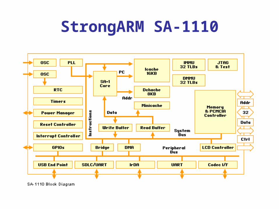
StrongARM SA-1110
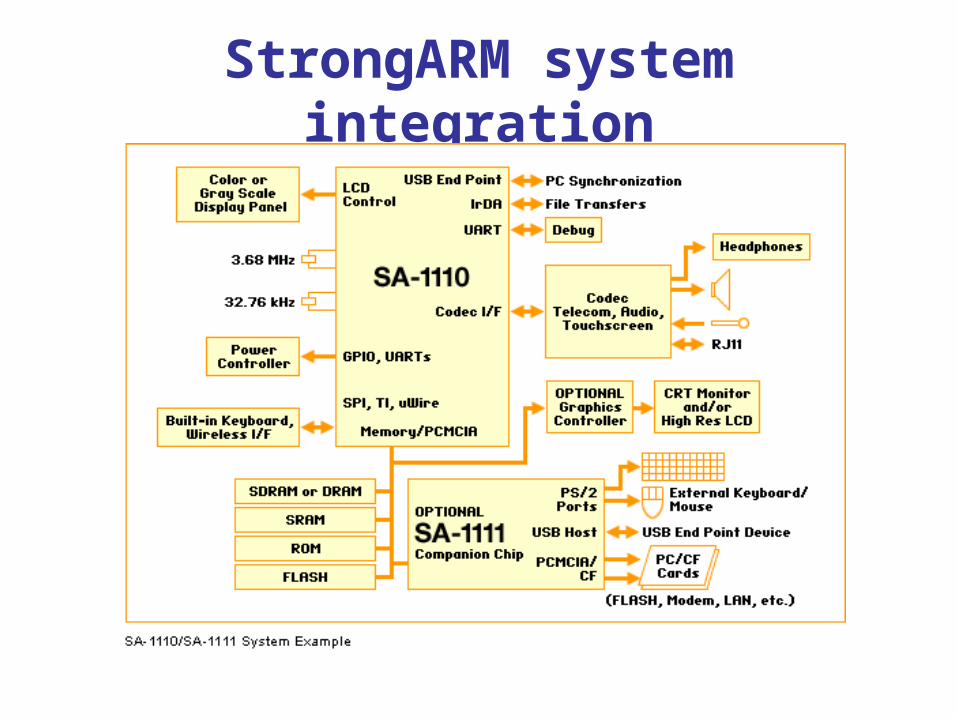
StrongARM system integration

StrongARM SA-1110
• 2.1 MIPS, 206 Mhz• Normal Mode 240 mW @ 1.55V/133
Mhz, 400 mW @ 1.75V/206 MHz• 32 way set associatve caches• 16 KB I-cache, 8 KB write-back D-
cache• 32 entry I and D MMUs• Read/Write buffer

Additional features in chipset
• Memory controller for ROM, flash, DRAM (SDRAM), SRAM
• LCD controller (1/2/4 bit gray scale or 8/12/16 bit color)
• UART, IrDA• Touch-screen, audio port• 6 channel DMA controller• 2-slot PCMCIA controller, 12 Mbps USB
controller• 28 general purpose I/O ports, Interrupt
controller• Real-time clock with interrupt capability• Power modes: Normal, Idle, Sleep
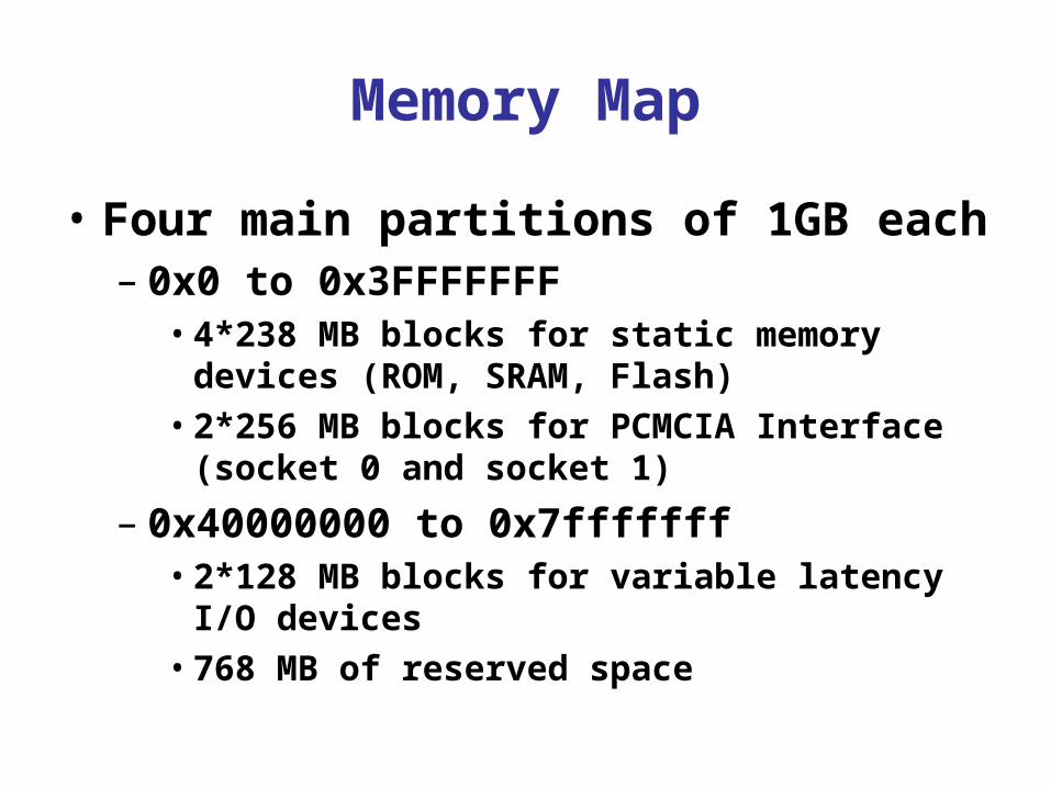
Memory Map
• Four main partitions of 1GB each– 0x0 to 0x3FFFFFFF
•4*238 MB blocks for static memory devices (ROM, SRAM, Flash)
•2*256 MB blocks for PCMCIA Interface (socket 0 and socket 1)
– 0x40000000 to 0x7fffffff•2*128 MB blocks for variable latency
I/O devices•768 MB of reserved space

Memory Map (contd.)
• 0x80000000 to 0xbfffffff– Contains all on-chip registers
(peripherals regs, sys control regs, memory regs, LCD and DMA regs)
• 0xc0000000 to 0xffffffff– 4*128MB of DRAM– 1*128MB mapped within memory
controller.– 384MB of reserved space
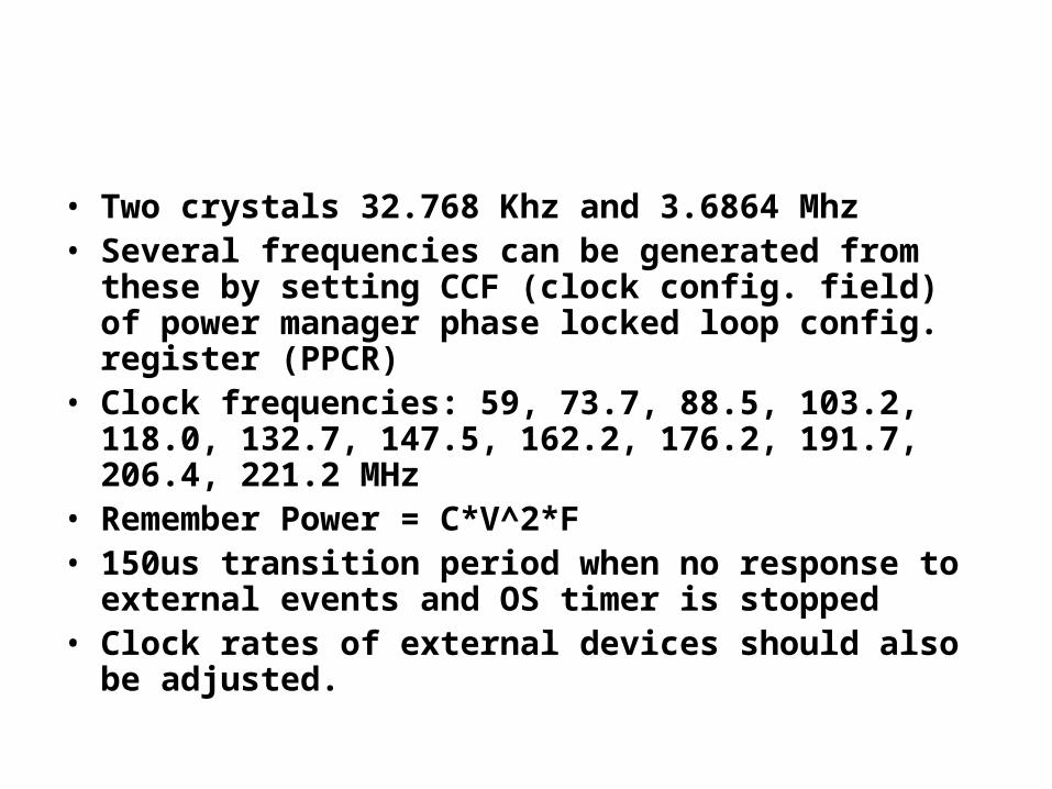
• Two crystals 32.768 Khz and 3.6864 Mhz• Several frequencies can be generated from
these by setting CCF (clock config. field) of power manager phase locked loop config. register (PPCR)
• Clock frequencies: 59, 73.7, 88.5, 103.2, 118.0, 132.7, 147.5, 162.2, 176.2, 191.7, 206.4, 221.2 MHz
• Remember Power = C*V^2*F• 150us transition period when no response to
external events and OS timer is stopped• Clock rates of external devices should also be
adjusted.
Memory Management
• Separate TLBs for instruction and data• Each has 32 entries that can each map
– Segment (1 MB)– Large page (8 KB)– Small Page (4 KB)
• Round-robin TLB replacement• Data TLB Support (Flush all, Flush entry)• Instruction TLB Support (Flush all)

Instruction Cache
• 16 KB, 32-way associative with 32 byte blocks
• Replacement is round robin within set
• I-cache operates with virtual addresses (both index and tag)
• Supports flush-all function

Data Cache
• 8KB, 32-way associative with 32 byte blocks. Round robin replacement in set
• Allocate only on loads• Flush all, flush entry and copyback
entry functions• Works with virtual addresses• 2 dirty bits per block for write-backs• In addition, a mini-data cache, which
can be used to hold data that can thrash in main data cache
• Mini data cache: 512 byte, 2-way

Data Cache vs Mini Data Cache
• Data can reside only in one of them and are searched in parallel
• Operation of load/store depends on B (bufferable) and C (cacheable) bits in MMU
• If C=1, data can be placed in either Normal or mini based on B bit for a load
• If B=0 (and C=1), load miss places block in mini cache
• If B=1 (and C=1), load miss places block in normal cache.

Write Buffer
• Can avoid stalling on writes• Upto 8 blocks of data of 1 to 16
bytes at different addresses• In the common case, writes are
not merged in the write buffer
Read Buffer
• Four entry read buffer capable of loading 1,4 or 8 words per entry
• Allows software to preload data into them for use at a later time without blocking the processor
• Software can also specify which entry to use. Portion of a block can be in one entry while rest can be in another entry – but a word can be in only one entry.
• Data can be simultaneously present in D-cache and Read buffer. Data is returned from Read buffer and software has to handle coherence issues.