Embed Size (px)
Citation preview

Radiation Detectors 1
Radiation Detectors
Outline
• Energy Resolution• Detection Efficiency• Dead Time• Scintillation Detector• Solid State Detectors• Germanium Gamma‐Ray Detectors
2
Energy Resolution
Energy Resolution
• For many applications it is important to measure the energy distribution of the incident radiation.
• These efforts are generally called “radiation spectroscopy”.
• One important property for spectroscopy can be seen in the detector response to a monoenergetic source of radiation.
• The differential pulse height distribution produced by a detector under these conditions is called the “response function” of the detector.
4
Radiation Detectors 2
Energy Resolution
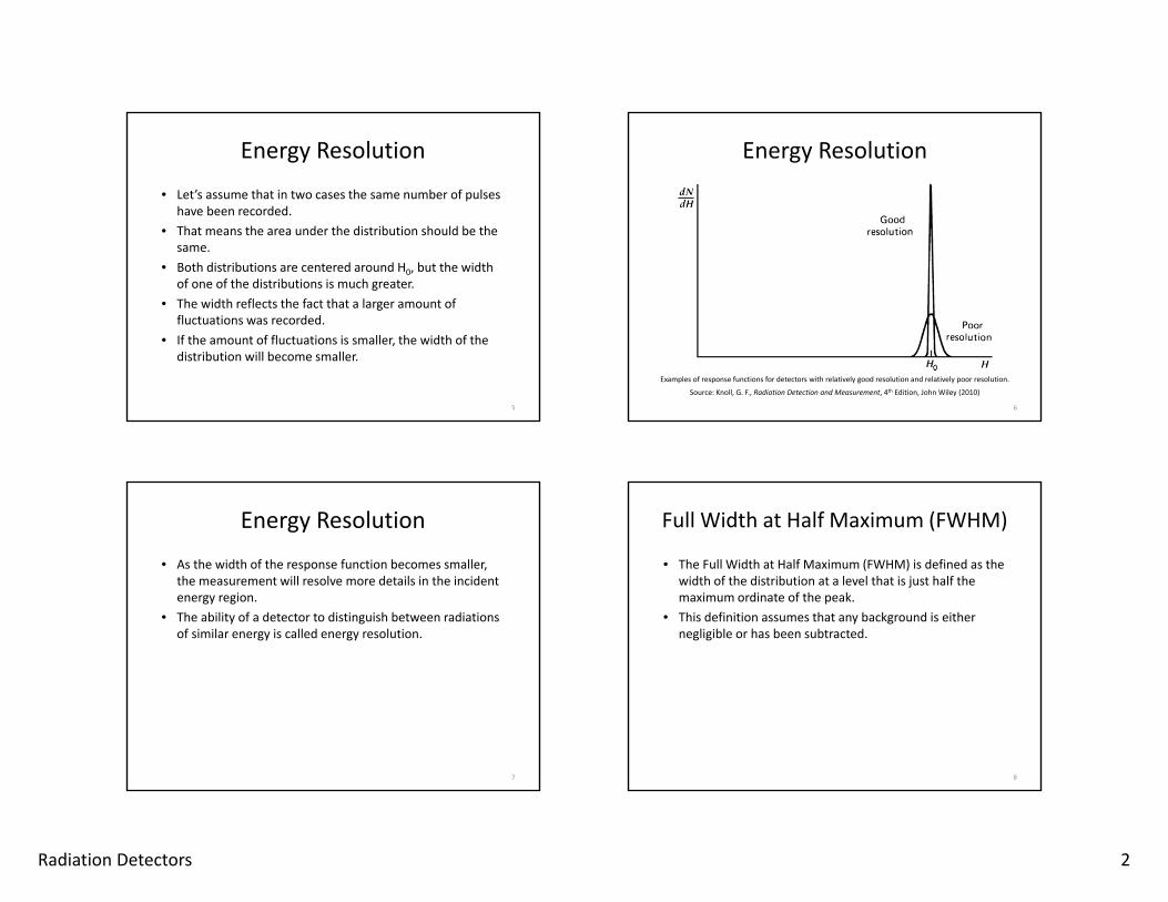
• Let’s assume that in two cases the same number of pulses have been recorded.
• That means the area under the distribution should be the same.
• Both distributions are centered around H0, but the width of one of the distributions is much greater.
• The width reflects the fact that a larger amount of fluctuations was recorded.
• If the amount of fluctuations is smaller, the width of the distribution will become smaller.
5
Energy Resolution
6
Examples of response functions for detectors with relatively good resolution and relatively poor resolution.
Source: Knoll, G. F., Radiation Detection and Measurement, 4th Edition, John Wiley (2010)
Energy Resolution
• As the width of the response function becomes smaller, the measurement will resolve more details in the incident energy region.
• The ability of a detector to distinguish between radiations of similar energy is called energy resolution.
7
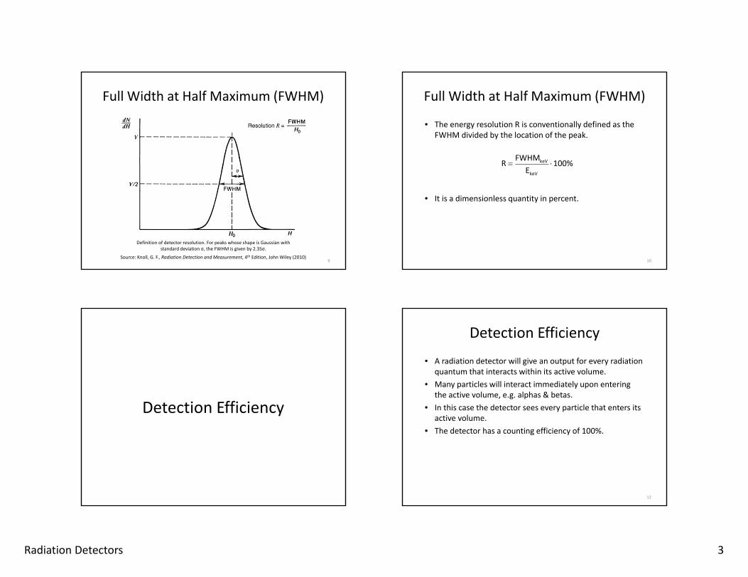
Full Width at Half Maximum (FWHM)
• The Full Width at Half Maximum (FWHM) is defined as the width of the distribution at a level that is just half the maximum ordinate of the peak.
• This definition assumes that any background is either negligible or has been subtracted.
8
Radiation Detectors 3
Full Width at Half Maximum (FWHM)
9
Definition of detector resolution. For peaks whose shape is Gaussian withstandard deviation σ, the FWHM is given by 2.35σ.
Source: Knoll, G. F., Radiation Detection and Measurement, 4th Edition, John Wiley (2010)
Full Width at Half Maximum (FWHM)
• The energy resolution R is conventionally defined as the FWHM divided by the location of the peak.
• It is a dimensionless quantity in percent.
100%E
FWHMR
keV
keV
10
Detection Efficiency
Detection Efficiency
• A radiation detector will give an output for every radiation quantum that interacts within its active volume.
• Many particles will interact immediately upon entering the active volume, e.g. alphas & betas.
• In this case the detector sees every particle that enters its active volume.
• The detector has a counting efficiency of 100%.
12

Radiation Detectors 4
Detection Efficiency
• On the other hand some radiations, e.g. photons and neutrons, must undergo a significant interaction before detection becomes possible.
• These types of radiation can travel large distances between interactions.
• As a result the detector may not see every particle that enters its active volume.
• In this case the detector efficiency will be less than 100%.
13
Detection Efficiency
• It is important to distinguish between two classes of counting efficiencies.
• The absolute efficiency is defined as:
• The intrinsic efficiency is defined as:
source by emitted quanta radiationof Numberrecorded pulsesof Number
ε
detector the entering quanta radiationof Numberrecorded pulsesof Number
ε
14
Dead Time
Dead Time• In most detector systems there is a minimum amount of
time necessary so that two separate events are recorded as two separate pulses.
• This limit is either due to processes in the detector or due to the response time of the electronics.
• The minimum time separation required is called the “dead time”.
• Because of the random nature of radioactive decay, there is always a chance that a true event is lost because it occurs to quickly after another.
16
Radiation Detectors 5
Dead Time
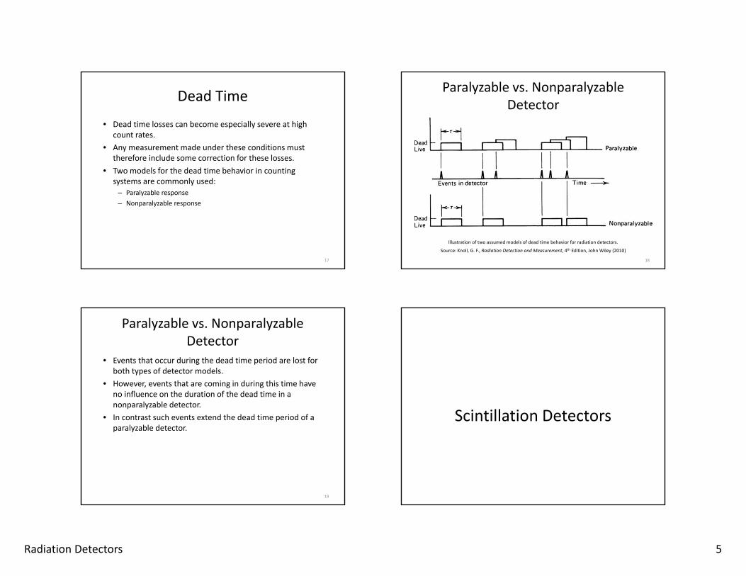
• Dead time losses can become especially severe at high count rates.
• Any measurement made under these conditions must therefore include some correction for these losses.
• Two models for the dead time behavior in counting systems are commonly used:
– Paralyzable response– Nonparalyzable response
17
Paralyzable vs. NonparalyzableDetector
18
Illustration of two assumed models of dead time behavior for radiation detectors.
Source: Knoll, G. F., Radiation Detection and Measurement, 4th Edition, John Wiley (2010)
Paralyzable vs. Nonparalyzable Detector
• Events that occur during the dead time period are lost for both types of detector models.
• However, events that are coming in during this time have no influence on the duration of the dead time in a nonparalyzable detector.
• In contrast such events extend the dead time period of a paralyzable detector.
19
Scintillation Detectors

Radiation Detectors 6
Introduction
• The detection of ionizing radiation by scintillation light is one of the oldest techniques known.
• It still remains one of the most useful methods for radiation detection and spectroscopy.
• It is widely used in gamma‐ray spectroscopy(NaI, LaBr3, BGO) and in beta, alpha and neutron counting (LSC).
• It can even be used for particle identification based on pulse shape analysis of the light pulse emitted.
21
Introduction
• Inorganic scintillators (high Z) are useful for gamma‐ray detection and spectroscopy as well as for detection of alpha and charged particles.
• They have the best light output and linearity, but they have a slow response time.
• Examples of inorganic scintillators are:– NaI CsI– BaF ZnS– BGO many, many more…
22
Introduction
• Organic scintillators (low Z) are useful for beta spectroscopy and fast neutron detection.
• They have a fast response time but yield less light.• Examples of organic scintillators are:
– Plastics– Liquid scintillators
23
Emission Processes
• Fluorescence is the prompt emission of visible radiation following excitation.
• Phosphorescence corresponds to emission at a longer wavelength over a longer period of time.
• Delayed fluorescence has the same emission as prompt fluorescence, but occurs over a much longer time period as well.
24

Radiation Detectors 7
Introduction
• A good scintillator should maximize the conversion of radiation to fluorescence.
• At the same time it should minimize the occurring phosphorescence and delayed fluorescence.
25
Organic ScintillatorsScintillation Mechanism
Organic Scintillators
• The fluorescence of organic scintillators is based on electron transitions between different energy levels.
• It is a molecular property and not a bulk property.• It can therefore be observed independent of the physical
state. • Many organic scintillators are based on molecules with π‐
bonds.
27
Organic Scintillators
• These are covalent chemical bonds involving p‐orbitals(double bonds, aromatic rings).
• Energy can be absorbed by exciting an electron into a number of different excited energy states.
28

Radiation Detectors 8
Electronic States
• Electronic states can be divided into singlet states S (spin 0) and triplet states T (spin 1).
• A series of singlet states is labeled as S0, S1, S2,…• The typical spacing between S0 and S1 is 3 – 4 eV.• Each singlet state is further divided into a number of
vibrational states. • S00 represents the lowest vibrational state.• At room temperature nearly all electrons are in the S00
state.
29
Electronic States
Energy levels of an organic molecule with π–electron structure.
Source: Knoll, G. F., Radiation Detection and Measurement, 4th Edition, John Wiley (2010)
30
Fluorescence
• Higher singlet states de‐excite quickly to S1 through radiationless internal conversion.
• After a short amount of time, a population of excited molecules in the S1 state is produced as result of the excitation through ionizing radiation.
• Scintillation light is emitted in transitions between S1 and one of the vibrational states of the ground state.
• This transition is the basis for fluorescence.
31
Phosphorescence
• Electrons from an excited singlet state can transfer to a triplet state through intersystem crossing.
• The lifetime for the first triplet state is much longer then that of the singlet state.
• Emission of light from a triplet state is therefore delayed. This is the basis for phosphorescence.
• T1 lies below S1, therefore the wavelength for phosphorescence is longer than for fluorescence.
32

Radiation Detectors 9
Delayed Fluorescence
• Some molecules in the T1 state may be thermally excited back into the S1 state and decay through fluorescence.
• This process gives rise to delayed fluorescence.
33
Wavelength & Absorption
The optical absorption and emission spectra for a typical organic scintillator with the level structure shown inthe previous figure.
Source: Knoll, G. F., Radiation Detection and Measurement, 4th Edition, John Wiley (2010) 34
Multi‐Component Scintillators
• In most organic materials, the excitation energy can be transferred to other molecules through collisions before de‐excitation occurs.
• This transfer is especially important for organic scintillators that involve more than one species of molecules.
• Let’s assume that a small concentration of an efficient scintillator is added to a bulk solvent.
• Then energy taken up by the solvent molecules can be transferred to the scintillator molecules through collisions between the molecules.
35
Multi‐Component Scintillators
• Once the energy has been transferred to a scintillator molecule, it can be emitted as light.
• Such binary organic scintillators are widely used both as liquid and plastic solutions.
• A third component is sometimes added to these mixtures to serve as a “waveshifter”.
• It works by absorbing the light from the primary scintillantand reradiating at a longer wavelength.
• This can be useful to match the emission spectrum closer to a photomultiplier tube.
36

Radiation Detectors 10
Quenching
• Scintillation efficiency is defined as the fraction of all incident particle energy that is converted to light.
• It should be as large as possible.• Any process that reduces the efficiency of the conversion
of particle energy into light is called “quenching”.• There are two types of quenching:
– Chemical quenching– Color quenching
37
Quenching
38
Source: Thomson, J., Use and Preparation of Quench Curves, Liquid Scintillation Counting Application NoteP11399, PerkinElmer (2002)
Quenching
• Chemical quenching is caused if the excited molecules have alternate de‐excitation modes available that do not involve the emission of light.
• In these cases the excitation energy is mainly converted to heat.
• Color quenching is caused if the photons emitted are prevented from being detected by the PMT.
• The photon may be absorbed or its wavelength could be changed so that the PMT is not sensitive to it anymore.
39
Inorganic ScintillatorsScintillation Mechanism

Radiation Detectors 11
Scintillation Mechanism
• Scintillation in inorganic materials is based on transitions between energy levels determined by the crystal lattice of the material.
• This is not a molecular process, it is instead based on the properties of the bulk material.
• In insulators, only discrete bands of energy are available to electrons.
41
Scintillation Mechanism
• The lower band is called the valence band.• It represents those electrons that are bound at lattice
sites.• The upper band is called the conduction band.• It represents the electrons that have enough energy to
move through the crystal.• The region between these to bands is called the forbidden
band.• In pure crystals electrons can not exist in this band.
42
Scintillation Mechanism
Energy band structure of a pure crystalline scintillator.
Source: Knoll, G. F., Radiation Detection and Measurement, 4th Edition, John Wiley (2010)
43
Scintillation Mechanism
• Absorption of energy results in the transfer of an electron from the valance to the conductive band.
• As a result a hole is created in the valence band.• In a pure crystal, return of the electron with emission of a
photon is an inefficient process.• Furthermore, the photon emitted would not be in the
visible range, because the width of the gap is generally to wide.
44
Radiation Detectors 12
Scintillation Mechanism
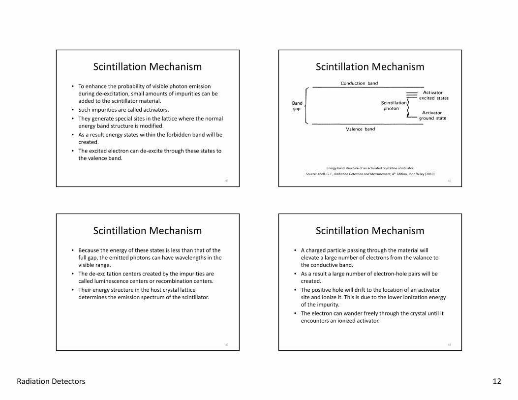
• To enhance the probability of visible photon emission during de‐excitation, small amounts of impurities can be added to the scintillator material.
• Such impurities are called activators.• They generate special sites in the lattice where the normal
energy band structure is modified.• As a result energy states within the forbidden band will be
created.• The excited electron can de‐excite through these states to
the valence band.
45
Scintillation Mechanism
Energy band structure of an activiated crystalline scintillator.
Source: Knoll, G. F., Radiation Detection and Measurement, 4th Edition, John Wiley (2010)
46
Scintillation Mechanism
• Because the energy of these states is less than that of the full gap, the emitted photons can have wavelengths in the visible range.
• The de‐excitation centers created by the impurities are called luminescence centers or recombination centers.
• Their energy structure in the host crystal lattice determines the emission spectrum of the scintillator.
47
Scintillation Mechanism
• A charged particle passing through the material will elevate a large number of electrons from the valance to the conductive band.
• As a result a large number of electron‐hole pairs will be created.
• The positive hole will drift to the location of an activator site and ionize it. This is due to the lower ionization energy of the impurity.
• The electron can wander freely through the crystal until it encounters an ionized activator.
48
Radiation Detectors 13
Scintillation Mechanism
• At this point the electron can drop into the activator site and form a neutral atom again.
• The electron is now in an excited state of an atom with its own set of excited energy states.
• If the excited state has an allowed transition to the ground state, de‐excitation will occur quickly through emission of a photon.
• If the activator is chosen properly, this transition can be in the visible range.
49
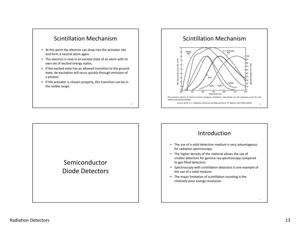
Scintillation Mechanism
The emission spectra of several common inorganic scintillators. Also shown are the response curves for twowidely used photocathodes.
Source: Knoll, G. F., Radiation Detection and Measurement, 4th Edition, John Wiley (2010) 50
SemiconductorDiode Detectors
Introduction
• The use of a solid detection medium is very advantageous for radiation spectroscopy.
• The higher density of the material allows the use of smaller detectors for gamma‐ray spectroscopy compared to gas‐filled detectors.
• Spectroscopy with scintillation detectors is one example of the use of a solid medium.
• The major limitation of scintillation counting is the relatively poor energy resolution.
52

Radiation Detectors 14
Introduction
• A series of events needs to occur to convert the incident radiation energy into light and finally into an electrical signal.
• This chain of events involves many inefficient steps.• The energy to produce one information carrier is on the
order of 100 eV or more.• Not more than a thousand carriers are created for a
typical interaction.
53
Introduction
• The statistical fluctuation in such a small number of carriers limits the energy resolution that can be achieved.
• It is impossible to improve the resolution beyond the limits set by statistics.
• The only way to improve the statistics limit is to increase the number of information carriers.
• The use of semiconductor materials as radiation detectors can result in a much larger number of information carriers for a given incident radiation.
54
Introduction
• Consequently, semiconductor detectors can achieve the best energy resolution of all detectors used for radiation spectroscopy.
• The information carriers created in the detector are electron‐hole pairs that are formed along the path of the incident radiation.
• The electron‐hole pair fulfills a purpose similar to an ion pair in gas‐filled detectors.
• The motion of the electron‐hole pairs in an electric field generates the basic electric signal.
55
Introduction
Semiconductor detectors have also several disadvantages:• Need to operate at low temperatures (liquid N2)
‐ True for GeLi and Ge detectors, but not for Si
• Lower intrinsic efficiency compared to NaI(Tl)‐ This is due to the lower Z of the detector material‐ Bigger crystals need to be fabricated
• Higher cost‐ Rough cost estimate: Efficiency x $1,000
• Susceptible to radiation damage
56

Radiation Detectors 15
Semiconductor Properties
Band Structure
• The lattice structure of crystalline materials creates allowed energy bands for the electrons in the solid.
• The energy of an electron in the pure material must be confined to one of these bands.
• The bands can be separated by gaps or ranges of forbidden energies.
58
Band Structure
• The lower band is called the valence band.• It represents those outer shell electrons that are bound to
lattice sites in the crystal.• In the case of Si or Ge, the electrons are part of a covalent
bond that constitutes the interatomic force in the crystal.• The upper band is called the conduction band.• It represents the electrons that are free to move through
the crystal.
59
Band Structure
60
Band structure for electron energies in insulators and semiconductors.
Source: Knoll, G. F., Radiation Detection and Measurement, 4th Edition, John Wiley (2010)

Radiation Detectors 16
Band Structure
• Electrons in the conduction band cause the electric conductivity of the material.
• The two bands are separated by the band gap or the forbidden band.
• A material is characterized as an insulator or a semiconductor based on the size of this band gap.
• For insulators the band gap is usually 5 eV or more. • For semiconductors it is considerably less (~ 1 eV).
61
Band Structure
• The number of electrons in the crystal band is just sufficient to fill all available sites in the valence band.
• In the absence of thermal excitation both insulators and semiconductors will have a full valence band and an empty conduction band.
• Under these conditions neither material shows any electric conductivity.
• The electron would have to cross the band gap to induce conductivity.
62
Band Structure
• In a metal the highest occupied energy band is not completely filled.
• Electrons can therefore easily migrate throughout the material.
• They only need to obtain a small amount of additional energy to be above the occupied states.
• Metals therefore always show a very high electrical conductivity.
63
Charge Carriers
• At any temperature above absolute zero, the electrons will have a certain thermal energy.
• In some cases this energy can be sufficient to elevate an electron from the valence band to the conduction band.
• Physically, this process means that an electron that is part of a covalent bond becomes excited.
• It is able to leave its bonding site in the lattice and drift through the crystal.
64

Radiation Detectors 17
Charge Carriers
• The excitation process creates an electron in the otherwise empty conduction band.
• As a result a vacancy is left in the otherwise full valence band.
• This vacancy is called a hole.• The combination of the two is called an electron‐hole pair.• It is the solid‐state analogue of an ion pair created in a gas.
65
Charge Carriers
• The electron in the conduction band will move if an electric field is applied.
• The hole, representing a net positive charge, will move as well.
• The hole will move in the opposite direction of the electron.
• The motion of these two charges contributes to the observed conductivity of the material.
66
Charge Carriers
• The probability per unit time of thermally creating an electron‐hole pair is given by:
where T = Absolute temperatureEg = Bandgap energyk = Boltzmann constantC = Proportionality constant characteristic of material
Tk2
EexpTCp(T) g2
3
67
Charge Carriers
• The probability for thermal excitation depends critically on the ratio of the band gap energy to the temperature.
• Materials with a large band gap have a low probability for thermal excitation and will exhibit the behavior of an insulator.
• If the band gap is small, thermal excitation will cause the material to behave like a semiconductor.
• If no electric field is applied, the thermally created pairs will recombine and an equilibrium will be established.
68

Radiation Detectors 18
Charge Carriers
• As T decreases, the factor exp(‐Eg / 2kT) becomes much smaller and thermal excitation decreases significantly.
• The band gap for Si is 1.115 eV.– For large energy deposition (heavy charged particles), the
detector can be used without cooling.– For small energy deposition (X‐ray or electron spectroscopy), the
detector needs to be cooled.
• Ge has a band gap of 0.665 eV. – The band gap is so small that the detector must always be cooled
to 77 K (liquid N2) to be used.
69
Migration of Charge Carriers
• If an electric field is applied to the semiconductor, both the electrons and the holes will start to migrate.
• The motion will be a combination of their random thermal velocity and a drift velocity parallel to the direction of the electric field.
• It is easy to visualize the motion of the electrons.• The fact that moving holes contribute to the conductivity
as well is less obvious.
70
Migration of Charge Carriers
• For a hole to move from one position to another, the remaining positive charge caused by the excited electron has to move.
• This is achieved if an electron moves from a different binding site to the vacancy to fill the hole.
• In this case the vacancy will now exist at the binding site from which the new electron moved.
• The hole has switched positions.
71
Migration of Charge Carriers
• In gases the mobility of the electron is much higher than that of the positive ion.
• In contrast, the mobility of electrons and holes in semiconductors are of the same order.
• At higher electric field values, the drift velocity increases more slowly with the field.
• Eventually, it becomes independent of increases in the electric field strength.
• At this point a saturated drift velocity is reached.
72

Radiation Detectors 19
Migration of Charge Carriers
73
Drift velocity as a function of electric field applied parallel to the {111} crystallographic direction. Absolutetemperature is the parameter for the different curves. (a) Electrons in silicon; (b) holes in silicon; (c) electronsin germanium; (d) holes in germanium.
Source: Knoll, G. F., Radiation Detection and Measurement, 4th Edition, John Wiley (2010)
Migration of Charge Carriers
• Semiconductor detectors are generally operated with a field strength high enough to reach a saturated drift velocity.
• The resulting drift velocity is on the order of 107 cm/s.• The time required to collect charge carriers over typical
dimensions of 0.1 cm or less will be under 10 ns.• Semiconductor detectors belong therefore to the fastest‐
responding radiation detector types.
74
Migration of Charge Carriers
75Source: Knoll, G. F., Radiation Detection and Measurement, 4th Edition, John Wiley (2010)
Effect of Impurities
• In a completely pure semiconductor, all electrons in the conduction band and all holes in the valence band would be caused by thermal excitation.
• In this case the number of electrons in the conduction band would be exactly the same as the number of holes in the valence band.
• This is due to the fact that each electron thermally elevated must leave a hole behind.
• Such a material is called an intrinsic semi‐conductor.
76

Radiation Detectors 20
Effect of Impurities
• The properties of such a material can be described theoretically.
• However, it is impossible to create such a material in reality.
• The electronic properties of real materials are typically dominated by the residual small levels of impurities in the material.
• This is true even for Si and Ge, the semiconductors with the highest purity available.
77
Effect of Impurities
• Let n represent the number of electrons present in the conduction band.
• Let p represent the number of holes present in the valence band.
• Then the equilibrium existing in an intrinsic semiconductor can be described as:
• The quantities ni and pi are called the intrinsic carrier densities.
ii pn
78
Effect of Impurities
• The densities will be lowest for materials with large band gap energy.
• The densities will also decrease with decreasing temperature.
• Intrinsic hole or electron density at room temperature:– Si: 1.5 x 1010 cm‐3
– Ge: 1.5 x 1013 cm‐3
79
n‐Type Semiconductors
• We will use Si as an example to describe the effect of doping on semiconductor properties.
• The behavior of Ge and other semiconductor materials is similar.
• Si is tetravalent.• It forms covalent bonds with the four closest neighboring
silicon atoms in the normal crystal.• Thermal excitation consists of breaking one of these
covalent bonds and leaving behind a hole.
80
Radiation Detectors 21
n‐Type Semiconductors
• However, there will be a small amount of impurities present in the material.
• These impurities can be residues remaining after the best available purification step.
• Or they could have been added intentionally to tailor the properties of the material.
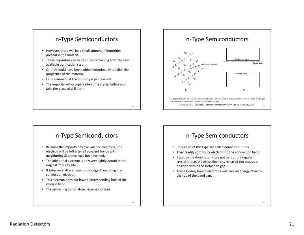
• Let’s assume that the impurity is pentavalent.• The impurity will occupy a site in the crystal lattice and
take the place of a Si atom.
81
n‐Type Semiconductors
82
(a) Representation of a donor impurity (phosphorus) occupying a substitutional site in a silicon crystal (b)Corresponding donor levels created in the silicon bandgap.
Source: Knoll, G. F., Radiation Detection and Measurement, 4th Edition, John Wiley (2010)
n‐Type Semiconductors
• Because the impurity has five valence electrons, one electron will be left after all covalent bonds with neighboring Si atoms have been formed.
• The additional electron is only very lightly bound to the original impurity site.
• It takes very little energy to dislodge it, resulting in a conduction electron.
• This electron does not have a corresponding hole in the valence band.
• The remaining donor atom becomes ionized.
83
n‐Type Semiconductors
• Impurities of this type are called donor impurities.• They readily contribute electrons to the conduction band.• Because the donor atoms are not part of the regular
crystal lattice, the extra electrons released can occupy a position within the forbidden gap.
• These loosely bound electrons will have an energy close to the top of the band gap.
84
Radiation Detectors 22
n‐Type Semiconductors
• The spacing between the valence band and the donor levels is small enough to ensure that a large fraction of the donor impurities are thermally excited.
• The concentration of impurities ND is normally always large compared with the number of intrinsic electrons in the conduction band.
• Therefore, the number of conduction electrons is dominated by the contribution from donor atoms.
DNn
85
n‐Type Semiconductors
• The added concentration of electrons in the conduction band shifts the equilibrium between electrons and holes through recombination.
• This means the equilibrium concentration of holes is decreased, so that the product of n and p is the same as for the intrinsic material.
ii pnpn
86
Example
• Intrinsic carrier density for Si: 1.5 x 1010 cm‐3
• Concentration of donor impurity: 1.0 x 1017 cm‐3
npnp ii
2250101.0
101.5101.5p 17
1010
87
n‐Type Semiconductors
• The total number of charge carriers is now much greater (1 x 1017 cm‐3 vs. 3 x 1010 cm‐3).
• The electrical conductivity of a doped material is therefore always significantly larger than that of pure material.
• Even though the conduction electrons greatly outnumber the holes, the material itself is still charge neutral.
• This is due to the presence of ionized donor atoms.
88
Radiation Detectors 23
n‐Type Semiconductors
• These lattice sites represent net positive charges that exactly balance the excess electrons.
• These positive lattice sites should, however, not be confused with holes.
• They are fixed in the lattice and cannot migrate.• The net effect of an n‐type material is to create a situation
in which the number of conduction electrons is much greater and the number of holes much smaller than in a pure material.
89
p‐Type Semiconductors
• The addition of a trivalent impurity to the material results in a very different situation.
• The impurity occupying a lattice site has one valence electron less than the neighboring atoms.
• This means one covalent bond with a neighbor cannot be formed.
• This vacancy represents a hole similar to that left behind when an electron is excited into the conduction band.
• It’s energy characteristics are slightly different.
90
p‐Type Semiconductors
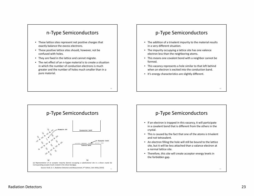
91
(a) Representation of an acceptor impurity (boron) occupying a substitutional site in a silicon crystal (b)Corresponding acceptor levels created in the silicon bandgap.
Source: Knoll, G. F., Radiation Detection and Measurement, 4th Edition, John Wiley (2010)
p‐Type Semiconductors
• If an electron is trapped in this vacancy, it will participate in a covalent bond that is different from the others in the crystal.
• This is caused by the fact that one of the atoms is trivalent and not tetravalent.
• An electron filling the hole will still be bound to the lattice site, but it will be less attached than a valance electron at a normal lattice site.
• Therefore, this site will create acceptor energy levels in the forbidden gap.
92
Radiation Detectors 24
p‐Type Semiconductors
• The new acceptor level will lie near the bottom of the gap, because the properties are similar to that of normal lattice sites.
• An impurity causing this type of energy levels in the forbidden gap is called an acceptor impurity.
• Because the energy difference between the valence band and the acceptor site is small, a large fraction of the acceptor sites will be filled with thermally excited electrons.
• These electrons come from normal sites in the lattice and will leave holes behind.
93
p‐Type Semiconductors
• Approximately one additional hole is created for every acceptor impurity added.
• If the concentrations of acceptor impurities NA is large compared to the concentration of intrinsic holes, then the number of holes will be dominated by the concentration of acceptors.
• The increased availability of holes increases the probability for recombination between electrons and holes.
ANp
94
p‐Type Semiconductors
• Therefore the number of equilibrium conduction electrons will be decreased.
• As a result, the electrical conductivity of a p‐type semiconductor is dominated by holes.
• Holes are the majority carriers and electrons are the minority carriers.
• The filled acceptor sites represent fixed negative charges.• They balance the positive charge of the additional holes.
95
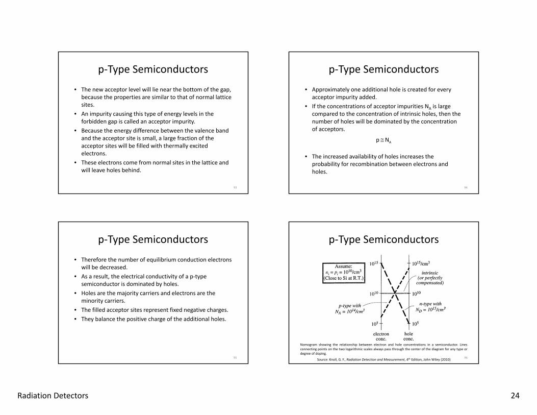
p‐Type Semiconductors
96
Nomogram showing the relationship between electron and hole concentrations in a semiconductor. Linesconnecting points on the two logarithmic scales always pass through the center of the diagram for any type ordegree of doping.
Source: Knoll, G. F., Radiation Detection and Measurement, 4th Edition, John Wiley (2010)
Radiation Detectors 25
Action of Ionizing Radiationin Semiconductors
Ionization Energy
• When a charged particle passes through a semi‐conductor, it will produce many electron‐hole pairs along its track.
• The amount of energy spent by the charged particle to create an electron‐hole pair is a very important quantity for detector applications.
• This quantity is often referred to as the ionization energy ε.
• It is largely independent of the energy and type of the incident radiation.
98
Ionization Energy
• This simplification allows to interpret the energy of the incident radiation in terms of the number of electron‐hole pairs produced.
• This only holds true if the radiation is completely stopped in the active volume of the detector.
• Interaction of radiation with a semiconductor always leads to the creation of the same number of electrons and holes.
• This is independent of the nature of the semi‐conductor (intrinsic, p‐ or n‐type).
99
Ionization Energy
• The same way equal numbers of electrons and positive ions are created in a gas, every conduction electron produced must leave behind a hole in the valence band.
• The concentration of doping materials are so low that they play no role in determining the photon interaction.
• p‐ and n‐type detectors of equal thickness have identical probabilities for gamma‐ray interaction.
• The range of particles will be the same in either type as well.
100
Radiation Detectors 26
Ionization Energy
• The great advantage of semiconductor detectors lies in their small ionization energy (~ 3 eV).
• For comparison, about 30 eV are required to produce an ion pair in gas‐filled detectors.
• The number of charge carriers produced for a given energy is therefore ten time greater in a semiconductor.
• The greater amount of charge carriers reduces the statistical fluctuations in the number of carriers.
• The greater charge per pulse also improves the signal‐to‐noise ratio for low energies.
101
Semiconductors asRadiation Detectors
Electrical Contacts
• In a radiation detector the charge produced must be collected at either boundary of the semiconductor material.
• This is usually done by applying some type of contact to the material.
• An ohmic contact is a non‐correcting electrode through which charges of either sign can flow.
• Typical ohmic contacts on semiconductors are sputtered or evaporated metal pads that are patterned using photolithography.
103
Electrical Contacts
• Lets assume a semiconductor with two ohmic contact fitted on opposite sides that are connected to a circuit.
• For each electron or hole collected at one electrode, the same species will be introduced at the other electrode.
• As a result, the equilibrium charge carrier concentration in the material will be maintained.
• Use of ohmic contacts causes leakage currents that are much too high to allow for their use in Si or Ge detectors.
104

Radiation Detectors 27
Electrical Contacts
• Instead, non‐injecting or blocking contacts are typically used to reduce leakage current.
• In this case the charge carriers initially removed by the application of an electric field are not replaced at the opposite electrode.
• Their overall concentration will therefore drop after application of an electric field.
• The leakage current can thus be reduced to a value that allows detection of the electron‐hole pairs created by ionizing radiation.
105
Electrical Contacts
• The best type of blocking contact are the two sides of a p‐n semiconductor junction.
• Holes are the majority carrier on the p‐side of the junction and free electrons are rare.
• This makes it very difficult to inject electrons from this side.
• On the opposite side, electrons are the majority carrier and holes are few.
• It is very difficult to inject holes from this side.
106
Electrical Contacts
• In this lecture we will concentrate on detectors created by placing a p‐type material in direct contact with a n‐type material.
• This is called a p‐n junction.
• In other detectors the p‐ and n‐type regions are separated by an intrinsic region (i‐region).
107
Semiconductor Junction
• The detectors described in this lecture are based on the properties created near a p‐n junction in semiconductors.
• If the regions are brought in good contact, then charge carriers are able to migrate across the junction.
• The junction cannot be created by just bringing together two pieces of p‐type and n‐type material.
• There would be gaps between them that are large compared with the interatomic lattice spacing.
108

Radiation Detectors 28
Semiconductor Junction
• Instead the junction is normally formed in a single crystal.• A change in impurity content is caused from one side of
the junction to the other.• Lets assume the process starts with a p‐type crystal that
has been doped with a uniform concentration of an acceptor impurity.
• The surface of the crystal is exposed to the vapor of an n‐type impurity that diffuses some distance into the crystal.
109
Semiconductor Junction
110
The assumed concentration profiles for the n‐p junction shown at the top are explained in the text. The effectsof carrier diffusion across the junction gives rise to the illustrated profiles for space charge p(x), electricpotential φ(x), and electric field ε(x).
Source: Knoll, G. F., Radiation Detection and Measurement, 4th Edition, John Wiley (2010)
Semiconductor Junction
• The resulting donor impurity concentration ND in the crystal decreases with distance from the surface.
• Near the surface, the concentration of donor atoms will be higher than that of acceptor atoms.
• This means this side of the crystal will become an n‐type material.
111
Semiconductors Detector Configurations

Radiation Detectors 29
Diffused Junction Detectors
• Fabrication of this type of detector starts with a homogenous crystal of a p‐type semiconductor.
• One surface of the material is exposed to the vapor of an n‐type impurity (typically P).
• This converts the region close to the surface to from a p‐type to an n‐type material.
• As a result a p‐n junction is formed some distance from the surface.
• The depth of the n‐type layer ranges from 0.1‐2.0 μm.
113
Diffused Junction Detectors
• Because the impurity concentration in the n‐type region is much higher than that in the p‐type region, the depletion region will extend mainly into the p‐side of the junction.
• This results in a surface layer that is not depleted and does not act as an active volume.
• It represents a dead layer through which the radiation must pass before it can be detected.
• This dead layer can cause a real disadvantage for charged particle spectroscopy.
114
Diffused Junction Detectors
• Part of the particle energy will be lost before the particle reaches the active detector volume.
• For this reason diffused junction detectors have been replaced in most applications.
• They are commercially still available and offer one advantage over surface barrier detectors.
• They are more rugged and are less affected by accumulation of impurities, e.g. oil, on the detector surface.
115
Surface Barrier Detectors
• Instead of using a p‐type material, a high density electron trap layer can be placed on the surface of an n‐type material.
• This results in a depletion region that behaves very much like that of a regular p‐n junction.
• The process to fabrication the electron trapping layer is mainly based on empirical observations.
• The procedure usually starts with etching the surface of the semiconductor.
116

Radiation Detectors 30
Surface Barrier Detectors
117
Source: ORTEC Advanced Measurement Technology, Inchttp://www.ortec‐online.com/download/Introduction‐Charged‐Particle‐Detectors.pdfretrieved April 24, 2012
Surface Barrier Detectors
• Afterwards a thin layer of gold is evaporated on the surface for electrical contact.
• The evaporation is carried out under conditions that promote oxidation of the surface layer.
• The resulting oxide layer between the gold and silicon plays an important role in determining the properties of the surface layer.
• Surface barrier detectors can also be produced by starting with a p‐type crystal and evaporating a layer of aluminum on the surface.
118
Surface Barrier Detectors
119
Construction and mounting of silicon junction detectors shown in cross‐sectional view. (a) Surface barriermount with coaxial connector (M) at rear. The silicon wafer (S) is mounted in a ceramic ring (I) with electricalcontact made between either side of the junction and opposite metalized surfaces of the ring. The frontsurface is connected to the outer case (C) and grounded, whereas the back surface is connected to the centerconductor of the coaxial connector. (b) Cutaway view of a transmission mount, in which both surfaces of thesilicon wafer are accessible. The coaxial connector is placed at the edge of the ceramic ring.
Source: Knoll, G. F., Radiation Detection and Measurement, 4th Edition, John Wiley (2010)
Surface Barrier Detectors
• The surface barrier detectors produced in this way have a very thin dead layer.
• Surface barrier detectors are sensitive to light.• Light photons striking the detector surface can reach the
active volume.• Light in the visible range has an energy of 2‐4 eV.• This is sufficient to create electron‐ hole pairs.• Exposure to normal room lighting would result in a very
high noise level in the detector.
120
Radiation Detectors 31
Surface Barrier Detectors
• Fortunately the vacuum enclosure necessary for most applications provides sufficient protection from light.
• Due to the thin entrance window the detector is also sensitive to damage from vapor exposure.
• The surface of this type of detector should never be handled directly.
• Because surface barrier detectors are usually created using n‐type crystals, a positive voltage has to be applied to achieve reverse biasing.
121
Ion Implanted Detectors
• Instead of exposing the surface of the detector to the vapor of a doping material, the material can be introduced through ion implantation.
• To produce n+ or p+ layers, the semiconductor is irradiated with accelerated ions, such as P or B.
• A fixed‐voltage accelerator produces mono‐energetic ions that have a well defined range in the material.
• By changing the accelerator voltage and the energy of the ions, the concentration profile of the impurity introduced can be controlled.
122
Ion Implanted Detectors
• After exposure to the ion beam the detector is usually annealed at elevated temperatures.
• This reduces the effect of radiation damage on the detector.
• The temperature needed to anneal the detector (< 500 °C) is significantly lower than the temperature required for thermal vapor diffusion.
• Ion implantation therefore results in less disturbance to the crystal structure.
123
Ion Implanted Detectors
124
Source: ORTEC Advanced Measurement Technology, Inchttp://www.ortec‐online.com/download/Introduction‐Charged‐Particle‐Detectors.pdfretrieved April 24, 2012

Radiation Detectors 32
Ion Implanted Detectors
• Ion implanted detectors tend to be more stable than surface barrier detectors.
• They are also less affected by ambient conditions.• Detectors are available with entrance windows as thin as
34 nm.
125
Passivated Planar Detectors
• The best currently available technique for the fabrication of silicon junction detectors combines the techniques of ion implantation and photo‐lithography.
• The technique is applied to a large‐area silicon waver.• This allows for the batch production of multiple detectors
simultaneously.• The process starts with a silicon waver that is slightly n‐
type due to residual impurities.
126
Passivated Planar Detectors
• The wafer is first cleaned and polished.• Then the surface is passified through creation of an oxide
layer at elevated temperatures.• Next photolithography is used to selectively remove areas
of the oxide layer where the entrance windows of the detectors will be located.
• A very thin layer inside the windows is converted into a p‐type material through boron ion implantation.
127
Passivated Planar Detectors
• The rear surface of the waver is converted into an n‐type material through implantation of a donor (As).
• This creates a blocking electrical contact.• Afterwards the waver is annealed at elevated temperature
to reduce radiation damage.• Finally aluminum is evaporated and patterned by photo
lithography to serve as a thin electrical contacts on the front and rear surfaces.
• Then the individual detectors are separated and encapsulated.
128

Radiation Detectors 33
Passivated Planar Detectors
129
Steps in the fabrication of passivated planar silicon diode detectors.
Source: Knoll, G. F., Radiation Detection and Measurement, 4th Edition, John Wiley (2010)
Passivated Planar Detectors
• The detectors produced have a very low leakage current and excellent operational characteristics.
• The junction edges are defined by the implantation process and are contained within the bulk wafer.
• In surface barrier detectors the junction will extend all the way to the edge of the wafer.
• The oxidation layer keeps leakage current much lower than with in surface barrier detectors.
130
Passivated Planar Detectors
• Leakage only occurs at the spots where the wafer is encapsulated in epoxy.
• Doping through ion implantation provides the detector with a very thin and uniform entrance window.
• This is important for good energy resolution.• The evaporated aluminum surface makes the detector
more rugged and it is less sensitive to damage.
131
Passivated Planar Detectors
www.canberra.com
132
Source: Canberra Industries, Inc. http://www.canberra.com/products/505.aspretrieved April 24, 2012

Radiation Detectors 34
GermaniumGamma‐Ray Detectors
Introduction
• The types of semiconductor detectors discussed previously are widely used for the detection of charged particle radiations.
• However, junction barrier detectors are not well suited for the detection of penetrating radiation.
• This is mainly due to the maximum depletion depth or active volume that can be achieved for such detectors.
• It is difficult to achieve a depletion depth of more than 2‐3 mm using semiconductor grade Si or Ge.
134
Introduction
• Detectors for gamma‐ray spectroscopy require a much larger active volume.
• This goal can be achieved through two different approaches.
• One approach is to purify the semiconductor material further to reach impurity concentrations of ~ 1010atoms/cm2.
• This would correspond to an impurity level of less than 1 part in 1012.
135
Introduction
• At this impurity level a depletion depth of 10 mm could be achieved with a bias of less than 1000 V.
• Production of material with this purity requires completely new refining techniques.
• Ultrapure crystals have been successfully created for Gebut not for Si.
• Detectors made from this ultrapure Ge are called High Purity Germanium Detectors (HPGe).
136
Radiation Detectors 35
Germanium Detector Configurations
HPGe Detector Fabrication
• The techniques for the production of ultrapure Ge were first developed in the 1970s.
• The process starts with bulk Ge intended for semiconductor production.
• This already very pure material is further processed using zone refining.
• A narrow zone of the material is locally heated and melts.• The wafer is then moved so that the molten zone passes
from one end of the crystal to the other.
138
HPGe Detector Fabrication
• The impurities are typically more soluble in the molten Gethan in the solid material.
• They therefore tend to accumulate in the molten zone and follow it through the crystal.
• The molten zone is allowed to solidify at one end of the wafer.
• It is then separated from the remaining crystal and discarded.
• By repeating this process impurity levels as low as 109atoms/cm3 have been achieved.
139
HPGe Detector Fabrication
3‐Coil Zone Refiner Zone‐Refined Ingot
140
Source: ORTEC Advanced Measurement Technology, Inchttp://www.ortec‐online.com/download/High‐Purity‐Germanium‐HPGe‐Detector‐Manufacturing.pdfretrieved April 28, 2012

Radiation Detectors 36
HPGe Detector Fabrication
• Large single crystals of germanium are grown using the Czochralski technique.
• A precisely cut seed crystal is dipped into the molten germanium and then withdrawn slowly.
• The temperature of the melt is maintained just above the freezing point during this process.
• The rate of crystal withdrawal and temperature of the melt are adjusted to control the growth of the crystal.
141
HPGe Detector Fabrication
Germanium CrystalBeing Grown
142
Source: ORTEC Advanced Measurement Technology, Inchttp://www.ortec‐online.com/download/High‐Purity‐Germanium‐HPGe‐Detector‐Manufacturing.pdfretrieved April 28, 2012
HPGe Detector Fabrication
• High‐purity germanium crystals suitable for detector fabrication are almost always grown in a quartz crucible under a hydrogen atmosphere.
• Near the completion of the growth process, the crystal is tapered gradually at the tail to minimize thermal strain.
• The crystal has to be grown to the exhaustion of the melt, because germanium both wets quartz and expands on freezing.
• The quartz crucible might be fractured if any Ge were left after completion of the crystal growth.
143
HPGe Detector Fabrication
• If the impurities remaining in the material are acceptors, the electrical properties of the material will be mildly p‐type.
• This material is often referred to as π–type.• Alternative, if donor impurities remain, the material will
be mildly n‐type.• Such a material is called υ–type.
144

Radiation Detectors 37
HPGe Detector Fabrication
• After the crystal is grown and cooled, it is mounted for slicing.
• The completed crystal is cut by a string saw that causes virtually no damage to the crystal.
• A slurry of water and silicon carbide is pulled along by a wire, resulting in a sawing action.
• Sections of the crystal from both top and bottom are checked to determine the impurity concentration and type (n or p).
• The part of the crystal which contains detector‐grade material is carefully selected.
145
HPGe Detector Fabrication
• The rejected material is returned to the zone refining operation.
• The crystal is then ground perfectly cylindrical.• The edge at one end is beveled to a radius to improve
charge collection and timing performance.• Afterwards, a hole is machined into the unbeveled end so
that the central contact of the device may be made later.• The detector subsequently is hand lapped all over to
remove damage from the machining processes.
146
HPGe Detector Fabrication
Mounted Crystal Being Sliced Grinding the Germanium Crystal
147
Source: ORTEC Advanced Measurement Technology, Inchttp://www.ortec‐online.com/download/High‐Purity‐Germanium‐HPGe‐Detector‐Manufacturing.pdfretrieved April 28, 2012
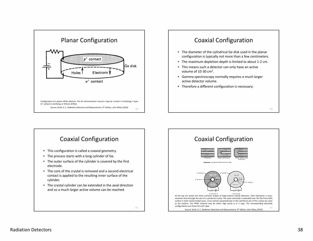
Planar Configuration
• In this configuration the electrical contacts are supplied to the two flat surfaces of a Ge disk.
• Typically a π‐material is used as starting material.• The n+ contact is created through either ion implantation
or lithium vapor diffusion of donor atoms on one surface.• The resulting n+‐p junction is reverse biased to form the
depletion region.• The contact on the opposite surface has to be non‐
injecting for the majority carriers.
148
Radiation Detectors 38
Planar Configuration
149
Configuration of a planar HPGe detector. The Ge semiconductor may be ν type (p+ contact is rectifying), π type(n+ contact is rectifying, or lithium drifted.
Source: Knoll, G. F., Radiation Detection and Measurement, 4th Edition, John Wiley (2010)
Coaxial Configuration
• The diameter of the cylindrical Ge disk used in the planar configuration is typically not more than a few centimeters.
• The maximum depletion depth is limited to about 1‐2 cm.• This means such a detector can only have an active
volume of 10‐30 cm3.• Gamma spectroscopy normally requires a much larger
active detector volume.• Therefore a different configuration is necessary.
150
Coaxial Configuration
• This configuration is called a coaxial geometry.• The process starts with a long cylinder of Ge.• The outer surface of the cylinder is covered by the first
electrode.• The core of the crystal is removed and a second electrical
contact is applied to the resulting inner surface of the cylinder.
• The crystal cylinder can be extended in the axial direction and so a much larger active volume can be reached.
151
Coaxial Configuration
152
At the top are shown the three common shapes of large‐volume coaxial detectors. Each represents a cross‐sectional view through the axis of a cylindrical crystal. The outer electrode is extended over the flat front (left)surface in both closed‐ended cases. Cross sections perpendicular to the cylindrical axis of the crystal are sownat the bottom. The HPGE material may be either high purity p or n type. The corresponding electrodeconfigurations are shown for each type.
Source: Knoll, G. F., Radiation Detection and Measurement, 4th Edition, John Wiley (2010)
Radiation Detectors 39
Coaxial Configuration
• In a closed‐ended coaxial configuration, only a part of the inner core is removed.
• In this case the outer electrode is extended over one flat surface of the crystal.
• This reduces leakage current from the front surface.• The electrode can be made very thin on the planar front
surface to serve as an entrance window for weakly penetrating radiations.
153
Coaxial Configuration
• The configuration can also be modified to allow physical access to the central bore.
• This is called a well configuration.• Small samples can be placed inside this well to be
measured.• In this geometry the source is almost completely
surrounded by the detector. • This can result in a very high detection efficiency.
154
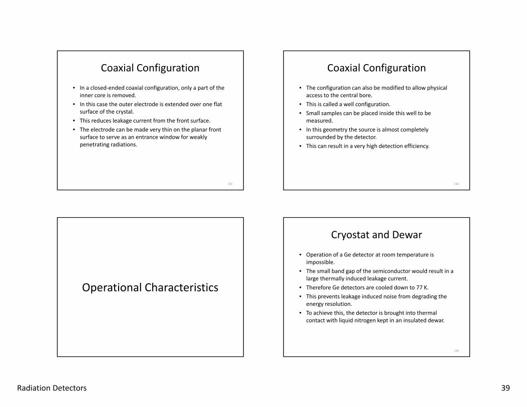
Operational Characteristics
Cryostat and Dewar
• Operation of a Ge detector at room temperature is impossible.
• The small band gap of the semiconductor would result in a large thermally induced leakage current.
• Therefore Ge detectors are cooled down to 77 K.• This prevents leakage induced noise from degrading the
energy resolution.• To achieve this, the detector is brought into thermal
contact with liquid nitrogen kept in an insulated dewar.
156
Radiation Detectors 40
Cryostat and Dewar
• The detector is housed in a vacuum‐tight cryostat to prevent thermal contact between the crystal and the surrounding air.
• The cryostat is typically evacuated and sealed by the manufacturer.
• However, a special port can be provided to allow additional pumping at a later time.
• A molecular sieve or a similar absorber is also placed into the sealed volume.
157
Cryostat and Dewar
• One end of the crystal is typically placed close to a thin end window to prevent attenuation of gamma rays.
• The cryostat can be mounted on the dewar in different configurations depending on the application.
• The most common configurations are horizontal or vertical.
• Typical dewars have a capacity of 30 L, so that the detector needs to be filled only once a week.
158
Cryostat and Dewar
• Such dewars are larger and heavier than the detector.• This makes portable operation impractical.• Many manufacturers provide smaller dewars for
applications that require a portable detector.• These dewars need to be filled much more frequently.• The latest generation of HPGe detectors uses electrical
coolers to eliminate or reduce the need for liquid nitrogen cooling.
159
Cryostat and Dewar
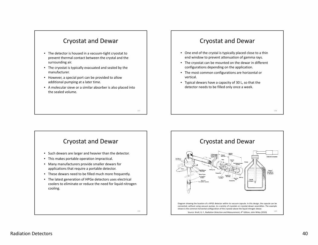
160
Diagram showing the location of a HPGE detector within its vacuum capsule. In this design, the capsule can beconnected, without using vacuum pumps, to a variety of cryostats or cryostat‐dewar assemblies. The exampleshown is the common horizontal configuration of the cryostat above the liquid nitrogen dewar.
Source: Knoll, G. F., Radiation Detection and Measurement, 4th Edition, John Wiley (2010)
Radiation Detectors 41
Energy Resolution
• As previously mentioned, the most important feature of germanium detectors is their excellent energy resolution.
• This property allows resolution of many closely spaced gamma lines that can not be resolved with scintillation detectors.
• Energy resolution is determined by:– Statistical variation in the number of charge carriers– Charge collection efficiency– Electronic noise
161
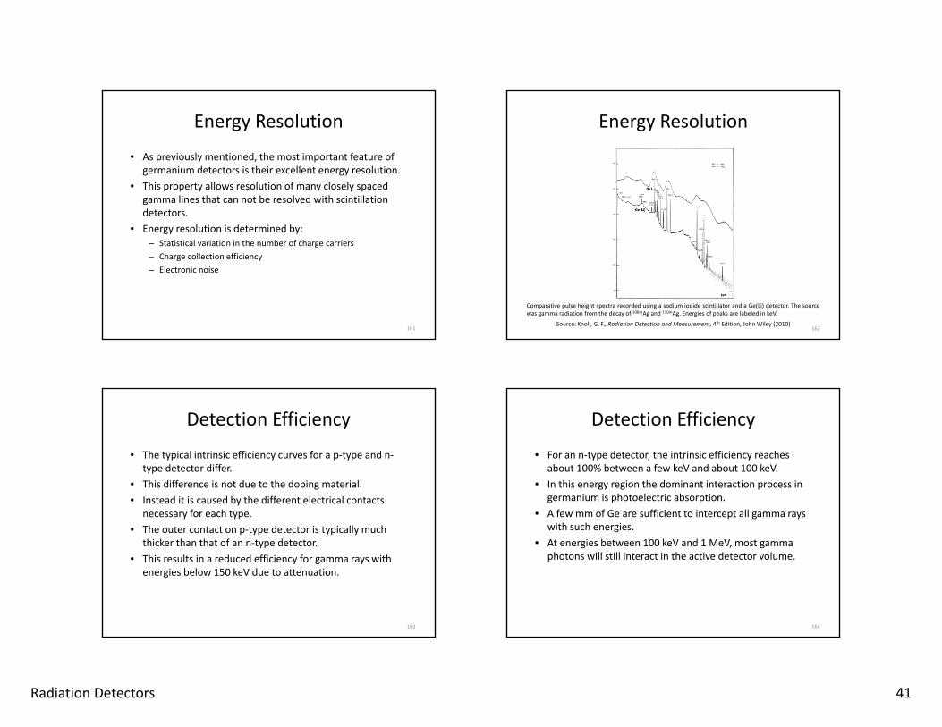
Energy Resolution
162
Comparative pulse height spectra recorded using a sodium iodide scintillator and a Ge(Li) detector. The sourcewas gamma radiation from the decay of 108mAg and 110mAg. Energies of peaks are labeled in keV.
Source: Knoll, G. F., Radiation Detection and Measurement, 4th Edition, John Wiley (2010)
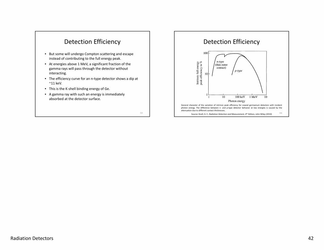
Detection Efficiency
• The typical intrinsic efficiency curves for a p‐type and n‐type detector differ.
• This difference is not due to the doping material.• Instead it is caused by the different electrical contacts
necessary for each type.• The outer contact on p‐type detector is typically much
thicker than that of an n‐type detector.• This results in a reduced efficiency for gamma rays with
energies below 150 keV due to attenuation.
163
Detection Efficiency
• For an n‐type detector, the intrinsic efficiency reaches about 100% between a few keV and about 100 keV.
• In this energy region the dominant interaction process in germanium is photoelectric absorption.
• A few mm of Ge are sufficient to intercept all gamma rays with such energies.
• At energies between 100 keV and 1 MeV, most gamma photons will still interact in the active detector volume.
164
Radiation Detectors 42
Detection Efficiency
• But some will undergo Compton scattering and escape instead of contributing to the full energy peak.
• At energies above 1 MeV, a significant fraction of the gamma rays will pass through the detector without interacting.
• The efficiency curve for an n‐type detector shows a dip at ~11 keV.
• This is the K‐shell binding energy of Ge.• A gamma ray with such an energy is immediately
absorbed at the detector surface.
165
Detection Efficiency
166
General character of the variation of intrinsic peak efficiency for coaxial germanium detectors with incidentphoton energy. The difference between n‐ and p‐type detector behavior at low energies is caused by theattenuation due to different contact thicknesses.
Source: Knoll, G. F., Radiation Detection and Measurement, 4th Edition, John Wiley (2010)