Embed Size (px)
Citation preview
Thermoreflectance imaging of electromigration evolution in asymmetric aluminumconstrictionsHao Tian, Woojin Ahn, Kerry Maize, Mengwei Si, Peide Ye, Muhammad Ashraful Alam, Ali Shakouri, and PeterBermel
Citation: Journal of Applied Physics 123, 035107 (2018);View online: https://doi.org/10.1063/1.5005938View Table of Contents: http://aip.scitation.org/toc/jap/123/3Published by the American Institute of Physics
Thermoreflectance imaging of electromigration evolution in asymmetricaluminum constrictions
Hao Tian,a) Woojin Ahn, Kerry Maize, Mengwei Si, Peide Ye, Muhammad Ashraful Alam,Ali Shakouri, and Peter BermelBirck Nanotechnology Center, Purdue University, West Lafayette, Indiana 47907, USA
(Received 20 September 2017; accepted 30 December 2017; published online 19 January 2018)
Electromigration (EM) is a phenomenon whereby the flow of current in metal wires moves the
underlying atoms, potentially inducing electronic interconnect failures. The continued decrease in
commercial lithographically defined feature sizes means that EM presents an increasing risk to the
reliability of modern electronics. To mitigate these risks, it is important to look for novel
mechanisms to extend lifetime without forfeiting miniaturization. Typically, only the overall
increase in the interconnect resistance and failure voltage are characterized. However, if the current
flows non-uniformly, spatially resolving the resulting hot spots during electromigration aging
experiments may provide better insights into the fundamental mechanisms of this process. In this
study, we focus on aluminum interconnects containing asymmetric reservoir and void pairs with
contact pads on each end. Such reservoirs are potential candidates for self-healing.
Thermoreflectance imaging was used to detect hot spots in electrical interconnects at risk of failure
as the voltage was gradually increased. It reveals differential heating with increasing voltage for
each polarity. We find that while current flow going from a constriction to a reservoir causes a
break at the void, the identical structure with the opposite polarity can sustain higher current
(J¼ 21� 106 A/cm2) and more localized joule heating and yet is more stable. Ultimately, a break
takes place at the contact pad where the current flows from narrow interconnect to larger pads. In
summary, thermoreflectance imaging with submicron spatial resolution provides valuable informa-
tion about localized electromigration evolution and the potential role of reservoirs to create more
robust interconnects. Published by AIP Publishing. https://doi.org/10.1063/1.5005938
I. INTRODUCTION
Electromigration (EM) is a phenomenon whereby strong
electric currents move the atoms in a wire, potentially induc-
ing electronic interconnect failures.1–3 As electrons move
from the cathode to the anode, they collide with metal ions
and transfer momentum to individual atoms, moving them in
the direction of the electron wind. This electron-associated
force can be so large under high current density that it will
overcome the confinement of the crystalline lattice and the
electric field in the metal wire.2,4 Gradually, the atoms in the
interconnect wires are displaced into hillocks and voids at
grain boundaries,5 which may cause severe problems in cir-
cuits, such as the fracturing of interconnects via large voids
and the formation of short circuits from hillocks. Previous
work has identified the basic phenomenology of EM failures
and mitigation strategies.6 For example, researchers have uti-
lized physical designs and optimized circuit designs to
reduce the current density,7–9 such as structures designed to
avoid current crowding and wiring topology optimization.
Some researchers have designed optimal architectures to
mitigate electromigration.10–12 For instance, when the wire
width is narrow enough, it forms bamboo-like grain bound-
ary structures which protect the atoms from moving with the
electron wind.4,6,13 For short interconnects below the so-
called Blech length (typically 10–100 lm), a mechanical
stress gradient is established along the line, helping the
atoms move against the electron wind.3,4,14,15 Copper doping
in the Al film has also been found to reduce electromigration
risk,16,17 which may retard atom transport along the grain
boundaries.16 In addition, the reservoir effect, which elon-
gates the lifetime of an interconnect by placing extra mate-
rial source near potential voids, has been studied for
electromigration mitigation.18,19
Although EM is now much better understood, the con-
tinuing decrease in commercial lithographically defined fea-
ture sizes has generally increased the current density, thus
raising the risk of more frequent EM failures.20 To mitigate
this risk, it is important to develop characterization methods
that can reveal localized current flow non-uniformities
and hot spots, as well as novel mechanisms that can extend
the lifetime without forfeiting miniaturization. Recently, the
observation of electromigration of Au nanowires in real time
has been implemented by Taychatanapat et al.21 using
scanning electron microscopy. Furthermore, the nanoscale
temperature distribution of Au nanowires during electromi-
gration has been studied by Jeong et al.,22 showing asymmet-
ric hotspot evolution and microvoid formation. In this
work, asymmetric constrictions and a potential self-healing
structure using the reservoir effect in a constant-volume line
are studied. The latter seeks to continually refill voids to
improve the reliability of interconnects. Specifically, a mate-
rial reservoir is placed near an intentionally added void on
the metal wire as shown in Fig. 1(a). The material we mainlya)Author to whom correspondence should be addressed: [email protected]
0021-8979/2018/123(3)/035107/8/$30.00 Published by AIP Publishing.123, 035107-1
JOURNAL OF APPLIED PHYSICS 123, 035107 (2018)
focus on is aluminum, which is commonly used in integrated
circuits and known to be susceptible to electromigration.23–25
Thermoreflectance imaging (TRI)26,27 is used to observe the
temperature spatial distribution and detect hot spots as the
stress level is increased. This provides a snapshot of the cur-
rent density profile in the device and the weak points that
eventually lead to breakdown. Compared with the scanning
thermal microscopy used by Jeong et al.,22 which scans point
by point, TRI possesses the advantages of being faster, thus
providing larger regions for detailed observation. Due to the
asymmetry of the designed devices, we find completely dif-
ferent electromigration failure modes for each bias polarity,
showing significantly different lifetimes. In addition, the
formation of hot spots is found to play an important role in
both the failure modes, which is related to electromigration-
induced structure degradation.
The methodology of this study is provided in Sec. II,
which includes fabrication of the test devices using photoli-
thography and lift-off processes and the thermoreflectance
imaging system used to characterize electromigration. The
results of forward polarity testing are then presented and ana-
lyzed in Sec. III, showing hotspot formation both near
the void and contact pad and the device breakdown at the
cathode contact pad. The case of reverse polarity is also
described for comparison, which is characterized by a shorter
lifetime, with failures occurring at the interconnect voids. In
Sec. IV, the reasons for asymmetry results are discussed to
help interpret the experimental results and provide guidance
for future electromigration investigation. Finally, the manu-
script concludes with Sec. V, which summarizes the main
findings of this study.
II. METHODS
The proposed asymmetric interconnect test structure is
illustrated in Fig. 1(a), which consists of an aluminum (Al)
test line with a void and reservoir pair that has the same aver-
age volume per unit length as the ordinary interconnect line
to which it is connected. Here, the interconnect line width is
5 lm, and the radius of the void and reservoir is 2 lm. It is
designed with a length of 1250 lm to provide reasonable
resistance in measurements. The device is fabricated on sili-
con dioxide (200 nm thickness), which is grown by thermal
dry oxidation on top of a standard Si wafer and serves as an
insulation layer. The fabrication procedure follows standard
photolithography and lift-off processes. A positive photore-
sist (AZ 1518) is first applied to the wafer using a G3 Wafer
Spinner, and the pattern is then transferred from the mask to
photoresist by exposing the wafer under UV light in the
mask aligner (Suss MA6 Mask Aligner, exposure of 13 s),
followed by development in the developer (AZ 340: ultra-
pure water ratio of 1:4) for 10–12 s. 110 nm Al is deposited
on the wafer using e-beam evaporation (CHA e-beam evapo-
rator) with a deposition rate of 3 A/s. Finally, the sample is
soaked in acetone until all the Al deposited on the photore-
sist is peeled off. During the soaking, the beaker containing
the wafer is placed in an ultrasonic water bath for 5–10 s,
which helps to lift-off the unwanted metal.
Figures 1(b) and 1(c) show the resulting optical micros-
copy images of the fabricated device. Since the total length
of the test line is relatively long, the actual device is rotated
as a serpentine line for better thermoreflectance imaging and
observation. Two different bias polarities are applied to the
device in this study, while the forward polarity is defined in
Fig. 1(b).
The principle of thermoreflectance imaging is illustrated
in Fig. 2(a).28,29 Electrical square wave pulses (pulse width
¼ 1 ms, duty cycle¼ 10%, and modulation frequency
¼ 100 Hz) are applied to the test line, inducing Joule heating in
the metal and a corresponding change in material reflectance.
FIG. 1. (a) Schematic of the asymmetric interconnect test structure, consist-
ing of a void and reservoir. The test line width is 5 lm, and the radius of the
void and reservoir is 2 lm. (b) Fabricated Al interconnect imaged via an
optical microscope. The definition of forward polarity is shown. (c)
Magnified view of the dashed white box from (b), showing the void and
reservoir.
FIG. 2. (a) Schematic of the principle of thermoreflectance imaging. Pulses
are applied to the device, while the reflectance of light is measured, which is
related to the temperature. The differential image between high and low
reflectance shows changes and distribution of the temperature. The inset
shows the typical temperature distribution of the whole device. (b)
Schematic of the thermoreflectance imaging system. An LED light is used to
illuminate the device, and a CCD is used to detect the reflected light from
the device. A computer synchronizes the triggering of the electrical signal
and detection of reflection. The current and voltage of the devices are moni-
tored by the oscilloscope using a four probe measurement.
035107-2 Tian et al. J. Appl. Phys. 123, 035107 (2018)
Separate experimental calibration of the aluminum temperature
coefficient of thermal reflectance (CTR) at the probe wave-
length of 780 nm yields a CTR value of 1.4 �10�4 per �C.
The spatial distribution of temperature is obtained by taking
the difference between the images acquired during the time
windows in the excitation waveform corresponding to the
device active (hot) and passive (equilibrium) states. Note that
the temperature measured is the temperature change (DT) rela-
tive to room temperature (approximately 25 �C). Figure 2(b)
shows the schematic of the Microsanj Inc. NT 210 thermore-
flectance imaging system used, which includes signal genera-
tion, probe illumination, CCD detection, and electrical
measurement systems. The sample wafer is placed on a copper
heat sink at the focal plane of a conventional reflectance
microscope. The device is electrically probed on the wafer
using a four-probe configuration. Pulsed probe light-emitting
diode (LED) illumination centered at 780 nm is coupled to the
microscope and illuminates the sample over the full field of
view. The sample reflected intensity is recorded using a 12-bit
Dalsa CCD coupled to the microscope. The device pulse wave-
form is generated by a function generator and amplified by a
current source. The device current and voltage during thermor-
eflectance excitation are monitored by an oscilloscope using a
four probe measurement. A Melles Griot 313 piezo actuator
and a custom Microsanj image registration algorithm automati-
cally correct for defocusing or image shift from thermal expan-
sion of the microscope during image averaging. All these
systems are synchronized by hardware triggers and processed
by Microsanj software. Since the device material reflectance
changes only slightly for the applied modulation, each image
is averaged over 10 min for a higher signal-to-noise ratio.
III. RESULTS AND ANALYSIS
A. Forward polarity
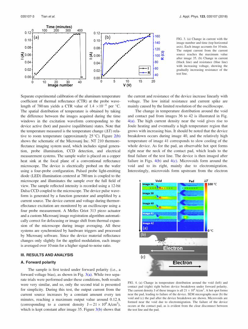
The sample is first tested under forward polarity (i.e., a
forward voltage bias), as shown in Fig. 3(a). While two sepa-
rate trials were performed under these conditions, both results
were very similar, and so, only the second trial is presented
for simplicity. During this test, the output current from the
current source increases by a constant amount every ten
minutes, reaching a maximum output value around 0.12 A
(corresponding to a current density J¼ 21� 106 A/cm2),
which is kept constant after image 35. Figure 3(b) shows that
the current and resistance of the device increase linearly with
voltage. The low initial resistance and current spike are
mainly caused by the limited resolution of the oscilloscope.
The change in temperature distribution around the void
and contact pad from images 36 to 42 is illustrated in Fig.
4(a). The high current density near the void gives rise to
Joule heating and eventually a high temperature region that
grows with increasing bias. It should be noted that the device
breakdown occurs during image 40, and the relatively high
temperature of image 41 corresponds to slow cooling of the
whole device. As for the pad, an observable hot spot forms
right near the neck of the contact pad, which leads to the
final failure of the test line. The device is then imaged after
failure in Figs. 4(b) and 4(c). Microvoids form around the
void and to its right, mainly due to electromigration.
Interestingly, microvoids form upstream from the electron
FIG. 3. (a) Change in current with the
image number and time (top horizontal
axis). Each image accounts for 10 min.
The output current from the current
source reaches the maximum value
after image 35. (b) Change in current
(black line) and resistance (blue line)
with increasing voltage, showing the
gradually increasing resistance of the
test line.
FIG. 4. (a) Change in temperature distribution around the void (left) and
contact pad (right) right before device breakdown under forward polarity.
The current density J of these images is all 21� 106 A/cm2. A hot spot forms
near the pad, leading to failure of the device. SEM micrographs near (b) the
void and (c) the pad after the device breakdown are shown. Microvoids are
formed near the void due to electromigration. The failure of the device
occurs at the contact pad, as is evident from the clear disconnect between
the test line and the pad.
035107-3 Tian et al. J. Appl. Phys. 123, 035107 (2018)
wind, in the high temperature region of Fig. 4(a). Although
some defects appear near the void, the device in fact fails at
the pad [Fig. 4(c)], caused by a disconnection between the
contact pad and wire line. Since defects are formed at both
locations, it is also possible that additional trials could yield
failures at the void in some cases.
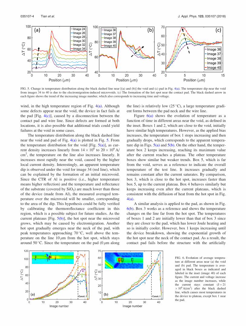
The temperature distribution along the black dashed line
near the void and pad of Fig. 4(a) is plotted in Fig. 5. From
the temperature distribution for the void [Fig. 5(a)], as cur-
rent density increases linearly from 14� 106 to 20� 106 A/
cm2, the temperature on the line also increases linearly. It
increases most rapidly near the void, caused by the higher
local current density. Interestingly, an apparent temperature
dip is observed under the void for image 34 (red line), which
can be explained by the formation of an initial microvoid.
Since the CTR of Al is positive (i.e., higher temperature
means higher reflection) and the temperature and reflectance
of the substrate (covered by SiO2) are much lower than those
of the device (made from Al), the measured averaged tem-
perature over the microvoid will be smaller, corresponding
to the area of the dip. This hypothesis could be fully verified
by calibrating the thermoreflectance coefficient in this
region, which is a possible subject for future studies. As the
current plateaus [Fig. 5(b)], the hot spot near the microvoid
grows, which may be caused by electromigration. Another
hot spot gradually emerges near the neck of the pad, with
peak temperatures approaching 70 �C, well above the tem-
perature on the line 10 lm from the hot spot, which stays
around 50 �C. Since the temperature on the pad (0 lm along
the line) is relatively low (25 �C), a large temperature gradi-
ent forms between the pad neck and the wire line.
Figure 6(a) shows the evolution of temperature as a
function of time in different areas near the void, as defined in
the inset. Boxes 1 and 2, which are close to the void, initially
have similar high temperatures. However, as the applied bias
increases, the temperature of box 1 stops increasing and then
gradually drops, which corresponds to the apparent tempera-
ture dip in Figs. 5(a) and 5(b). On the other hand, the temper-
ature box 2 keeps increasing, reaching its maximum value
after the current reaches a plateau. The other temperature
boxes show similar but weaker trends. Box 5, which is far
from the void, serves as a reference to indicate the overall
temperature of the test line. It increases gradually and
remains constant after the current saturates. By comparison,
box 3, which is close to the hot spot, increases faster than
box 5, up to the current plateau. Box 4 behaves similarly but
keeps increasing even after the current plateaus, which is
consistent with the diffusion of heat from the hot spot in Fig.
4(a).
A similar analysis is applied to the pad, as shown in Fig.
6(b). Box 3 works as a reference and shows the temperature
changes on the line far from the hot spot. The temperatures
of boxes 1 and 2 are initially lower than that of box 3 since
they are closer to the pad, which has lower Joule heating and
so is initially cooler. However, box 1 keeps increasing until
the device breakdown, showing the exponential growth of
the hot spot near the neck of the contact pad. As a result, the
contact pad fails before the structure with the artificially
FIG. 5. Change in temperature distribution along the black dashed line near [(a) and (b)] the void and (c) pad in Fig. 4(a). The temperature dip near the void
from images 34 to 40 is due to the electromigration-induced microvoids. (c) The formation of the hot spot near the contact pad. The black dashed arrow in
each figure shows the trend of the increasing image number, which also corresponds to increasing time and voltage.
FIG. 6. Evolution of average tempera-
ture at different areas near (a) the void
and (b) pad. The temperature is aver-
aged in black boxes as indicated and
labeled in the inset (image 40) of each
figure. The current and voltage increase
as the image number increases, while
the current stays constant (J¼ 21
� 106 A/cm2) after the black dashed
line, which causes most temperatures in
the device to plateau, except box 1 near
the pad.
035107-4 Tian et al. J. Appl. Phys. 123, 035107 (2018)

introduced void. This behavior may relate to microvoid for-
mation from electromigration, which causes local structure
and current density changes. The ultimate failure at the con-
tact pad implies that the reservoir may help preserve the
functionality of the central artificial void in this polarity.
Because the contact pad fails before the void in these trials,
the precise improvement at the level of reliability of the arti-
ficial void cannot be fully quantified. Moreover, a high tem-
perature gradient between the pad and wire line would
accelerate the degradation and void formation near the cath-
ode contact pad.30 It is interesting to note that the hot spot
with the highest absolute temperature along the interconnect
is not the one that fails first. Thus, the local structure, the
current density, and the temperature gradient should be con-
sidered in a manner that goes beyond Black’s equation.1
The resistivity of Al increases linearly with tempera-
ture,31 as can be seen in Fig. 7(a), based on box 5 tempera-
ture data in Fig. 6(a). Since the interconnect is relatively
long, the influence of electromigration-induced local resis-
tance changes is not evident at first. To further investigate
the main cause of the temperature rise, the relation between
temperature and Joule heating is illustrated in Fig. 7(b).
Three different areas are studied: the hot spots near the void
(void 2) and the pad (pad 1), as well as the area on the line
far from these hot spots (void 5). All temperatures increase
linearly with Joule power at different rates, which are related
to local conditions such as current density and thermal con-
duction. However, while the average interconnect line
reaches a temperature plateau after current saturation (void
5), the temperature of the two hot spots increases beyond the
general Joule power of the whole device. This is highly
related to the electromigration-induced local structural defor-
mation, which in turn affects the current distribution and
accelerates the hotspot growth.
B. Reverse polarity
Next, the device is tested at reverse polarity with other
conditions unchanged. In contrast with the case of forward
polarity, the breakdown occurs here before the current satu-
rates [Fig. 8(a)], and the device fails near the artificial void
instead of the contact pad. While two separate trials were
performed, both results were very similar, and so, only the
second trial is presented for simplicity. As shown in Fig.
8(b), the resistance also increases gradually, as Joule heating
raises the device temperature. This also creates a hot spot
near the void that grows rapidly as current density increases
[Fig. 9(a)]. At the beginning of image 32, the device breaks
immediately when the current density is increased to
19� 106 A/cm2. Then, it cools down, which pulls down the
average temperature of image 32. However, the hot spot near
the void can still be seen clearly in image 32. Figure 9(b)
shows a micrograph of the void region after failure, which
shows the microvoids induced by electromigration. The slit-
like void shape may be due to the electromigration-induced
diffusion along the void surface32,33 and is influenced by the
orientation of crystallographic surface planes and grain
boundaries in the metal.34–36
The cross-sectional temperature distribution along the
black dashed line in Fig. 9(a) is plotted in Fig. 10(a), show-
ing increasing temperature with time. The temperature of the
hot spot is greater than the surrounding line by more than
25 �C, and increases more quickly with applied voltage.
FIG. 7. (a) Resistance as a function of
the temperature of box 5, which repre-
sents the average temperature of the
whole device. The measured resistance
saturates with the limits of the current
source. (b) Dependence of temperature
on Joule heating power for box 2 (red
circle) and box 5 (black circle) near
the void and for box 1 (blue circle) of
the pad in Fig. 6. The blue arrow cap-
tures a temperature rise at the hot spot
near the pad that goes beyond Joule
heating. The corresponding dashed
lines in the figures are added only as
the guide to the eye.
FIG. 8. (a) Change in current with the
image number and time (top horizontal
axis). Each image accounts for 10 min.
(b) Change in current (black line) and
resistance (blue line) with increasing
voltage. In this test, the current
increases linearly without reaching the
maximum output of the current source.
035107-5 Tian et al. J. Appl. Phys. 123, 035107 (2018)
Interestingly, for image 31, an apparent temperature dip
under the void emerges, presumably because of microvoid
formation, which was also seen in the case of forward polar-
ity (Fig. 5). Figure 10(b) shows the temperature distribution
perpendicular to the test line, along red dashed lines in Fig.
9(a). Cross-section 1 in the upper left serves as a reference
for temperature increases far from the hot spot. Cross-
section 2 in the upper right shows the highest temperature,
which is in the middle of the initial hot spot. Although cross-
section 3 on the lower left is in the narrowest region of the
void, it is slightly cooler than the hot spot. Intriguingly, the
device does not break at the hottest area but rather at a sec-
ondary hot spot at cross-section 4 (in the lower right), which
may match the microvoid formation. From its temperature
changes, we can see that there is a large temperature jump at
image 31, which may weaken the strength of the intercon-
nection. On the other hand, the accelerated temperature
increase is highly related to the local structure deformation
(e.g., microvoids) caused by electromigration, and the
current density increases in the narrow region around
microvoids.
The evolution of temperature around the void is also
analyzed as a function of time, as shown in Fig. 11. Four dif-
ferent areas, labeled in the inset, are plotted here. As the
applied power increases, the temperatures of all regions rise
with Joule heating. As expected, box 4, which is far from the
void, has the lowest temperature and shows the overall tem-
perature changes of the whole device. Box 2 illustrates the
growth of the hot spot, which is heated the most by the local
current density distribution. Boxes 1 and 3 show tempera-
tures similar to box 4 initially but deviate from its trend over
time. Box 3 shows a slightly higher temperature since it is
closer to the hot spot, while box 1 exhibits more dramatic
increases after image 29, which also corresponds to the tem-
perature jump of cross-section 4 in Fig. 10(b). It is the forma-
tion of this secondary hot spot that leads to the failure of the
device (Fig. 9), which plays a similar role to the hot spot
near the contact pad in forward polarity.
As in the case of forward polarity, the increased resis-
tance is mainly due to the temperature dependent resistivity
of Al [Fig. 12(a)]. The dependency of temperature on Joule
heating for different areas is illustrated in Fig. 12(b). While
the temperature on the line (void 4) exhibits a linear depen-
dence on Joule heating, the initial (void 2) and the secondary
FIG. 9. (a) Change in temperature distribution around the void right before
the device breakdown under reverse polarity. The hot spot formed near the
void leads to the failure of the device. (b) SEM micrograph near the void
after the device breakdown. Microvoids are formed near the void due to
electromigration.
FIG. 10. (a) Change in temperature
distribution along the black dashed
line near void in Fig. 9(a). The black
dashed arrow shows the trend of the
increasing image number, correspond-
ing to increasing time. (b) Temperature
distribution along red dashed lines per-
pendicular to the test line as labeled in
Fig. 9(a). Each subfigure is numbered
following the definition in Fig. 9(a),
and its legend is the same with (a). The
black dashed lines indicate the bound-
ary of the device.
FIG. 11. Evolution of the average temperature of different areas near the
void. The temperature is averaged in black boxes as indicated and labeled in
the inset (image 31). Box 4 is added as an indication of the overall tempera-
ture of the device for reference. The increase in the image number corre-
sponds to the stress level increase applied to the device.
035107-6 Tian et al. J. Appl. Phys. 123, 035107 (2018)
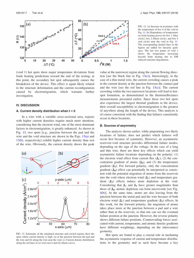
(void 1) hot spots show major temperature deviations from
Joule heating predictions toward the end of the testing; at
this point, the secondary hot spot subsequently causes the
breakdown of the device. This effect is again likely related
to the structure deformation and the current reconfiguration
caused by electromigration, which warrants further
investigation.
IV. DISCUSSION
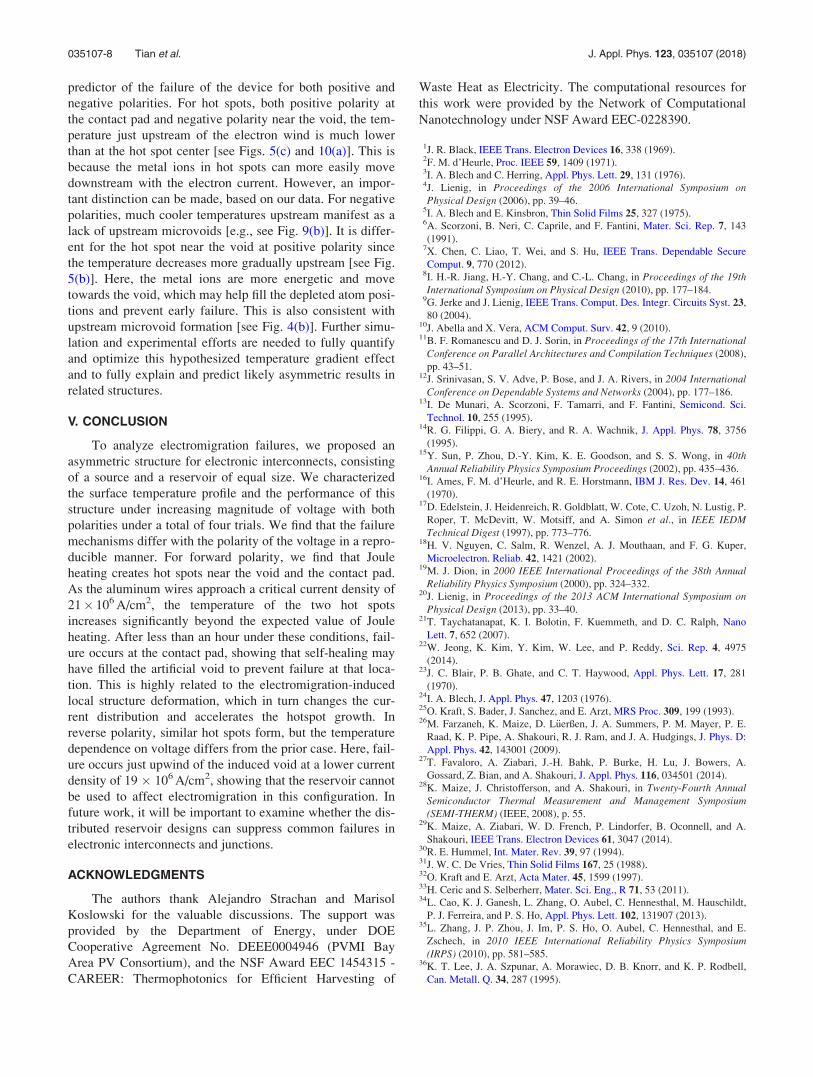
A. Current density distribution when t 5 0
In a wire with a variable cross-sectional area, regions
with higher current densities require much more attention,
considering that the electron wind, one of the most dominant
factors in electromigration, is greatly enhanced. As shown in
Fig. 13, two spots [e.g., junction between the pad and the
wire and the void structure are shown in the Figs. 13(a) and
13(b), respectively] exhibit higher current density than rest
of the wire. Obviously, the current density shows the peak
value at the narrowest region along the current flowing direc-
tion [see the black line in Fig. 13(c)]. Interestingly, in the
case of a thin metal wire, the current crowding causes a peak
in the current density at the junction between the contact pad
and the wire [see the red line in Fig. 13(c)]. The current
crowding within the two narrowest locations will lead to hot-
spot formation, as demonstrated in the thermoreflectance
measurements presented earlier. Since these two hot spots
also experience the largest thermal gradients in the device,
their overall susceptibility to electromigration is the greatest
of anywhere along the length of the device. This analysis is
of course consistent with the finding that failures consistently
occur in these locations.
B. Sources of asymmetry
The analysis shown earlier, while pinpointing two likely
locations of failure, does not predict which failures will
occur first because of symmetry. However, an asymmetric
reservoir-void structure provides differential failure modes,
depending on the sign of the voltage. In the case of a long
and thin wire, there are three key effects which can yield
asymmetric failure locations depending on the polarity: (1)
the electron wind effect from current flux (JC), (2) the con-
centration gradient of atoms (JD), and (3) the temperature
gradient (JT). For forward polarity, only the concentration
gradient (JD) effect can potentially be interpreted as consis-
tent with the potential migration of atoms from the reservoir
into the void where electron wind (JC) and temperature gra-
dient (JT) effects induce atom depletion at the void.
Considering that JC and JT have greater magnitudes than
those of JD, atomic depletion can form microvoids [see Fig.
4(b)]. At the same time, atoms are also leaving from the
junction between the metal pad and the wire because of both
electron wind (JC) and temperature gradient (JT) effects. In
this work, for the forward polarity, the migration of atoms
takes place more at the junction between a pad and a wire
rather than at the reservoir, so that one can see the eventual
failure position at the junction. However, the reverse polarity
shows different failure positions. Countervailing forces asso-
ciated with current, temperature, and atomic density gradients
have different weightings, depending on the interconnect
geometry.
Hot spots are found to play a crucial role in mediating
the asymmetric response of current and temperature distribu-
tions to the geometry and as such have become a key
FIG. 12. (a) Increase in resistance with
the temperature of box 4 of the void in
Fig. 11. (b) Dependence of temperature
on Joule heating power for box 1 (blue
circle), box 2 (black circle), and box 4
(red circle) near the void in Fig. 11.
The corresponding dashed lines in the
figures are added for linearity guid-
ance. The last two points of void 1
shows the temperature increasing
beyond Joule heating due to EM
induced structure degradation.
FIG. 13. Schematic of the simulated structure and circled regions show the
spots where current density is high: (a) at the junction between the pad and
the wire and (b) along the wire near the void. (c) Current density distribution
along the red lines in (a) (red curve) and (b) (black curve).
035107-7 Tian et al. J. Appl. Phys. 123, 035107 (2018)
predictor of the failure of the device for both positive and
negative polarities. For hot spots, both positive polarity at
the contact pad and negative polarity near the void, the tem-
perature just upstream of the electron wind is much lower
than at the hot spot center [see Figs. 5(c) and 10(a)]. This is
because the metal ions in hot spots can more easily move
downstream with the electron current. However, an impor-
tant distinction can be made, based on our data. For negative
polarities, much cooler temperatures upstream manifest as a
lack of upstream microvoids [e.g., see Fig. 9(b)]. It is differ-
ent for the hot spot near the void at positive polarity since
the temperature decreases more gradually upstream [see Fig.
5(b)]. Here, the metal ions are more energetic and move
towards the void, which may help fill the depleted atom posi-
tions and prevent early failure. This is also consistent with
upstream microvoid formation [see Fig. 4(b)]. Further simu-
lation and experimental efforts are needed to fully quantify
and optimize this hypothesized temperature gradient effect
and to fully explain and predict likely asymmetric results in
related structures.
V. CONCLUSION
To analyze electromigration failures, we proposed an
asymmetric structure for electronic interconnects, consisting
of a source and a reservoir of equal size. We characterized
the surface temperature profile and the performance of this
structure under increasing magnitude of voltage with both
polarities under a total of four trials. We find that the failure
mechanisms differ with the polarity of the voltage in a repro-
ducible manner. For forward polarity, we find that Joule
heating creates hot spots near the void and the contact pad.
As the aluminum wires approach a critical current density of
21� 106 A/cm2, the temperature of the two hot spots
increases significantly beyond the expected value of Joule
heating. After less than an hour under these conditions, fail-
ure occurs at the contact pad, showing that self-healing may
have filled the artificial void to prevent failure at that loca-
tion. This is highly related to the electromigration-induced
local structure deformation, which in turn changes the cur-
rent distribution and accelerates the hotspot growth. In
reverse polarity, similar hot spots form, but the temperature
dependence on voltage differs from the prior case. Here, fail-
ure occurs just upwind of the induced void at a lower current
density of 19 � 106 A/cm2, showing that the reservoir cannot
be used to affect electromigration in this configuration. In
future work, it will be important to examine whether the dis-
tributed reservoir designs can suppress common failures in
electronic interconnects and junctions.
ACKNOWLEDGMENTS
The authors thank Alejandro Strachan and Marisol
Koslowski for the valuable discussions. The support was
provided by the Department of Energy, under DOE
Cooperative Agreement No. DEEE0004946 (PVMI Bay
Area PV Consortium), and the NSF Award EEC 1454315 -
CAREER: Thermophotonics for Efficient Harvesting of
Waste Heat as Electricity. The computational resources for
this work were provided by the Network of Computational
Nanotechnology under NSF Award EEC-0228390.
1J. R. Black, IEEE Trans. Electron Devices 16, 338 (1969).2F. M. d’Heurle, Proc. IEEE 59, 1409 (1971).3I. A. Blech and C. Herring, Appl. Phys. Lett. 29, 131 (1976).4J. Lienig, in Proceedings of the 2006 International Symposium onPhysical Design (2006), pp. 39–46.
5I. A. Blech and E. Kinsbron, Thin Solid Films 25, 327 (1975).6A. Scorzoni, B. Neri, C. Caprile, and F. Fantini, Mater. Sci. Rep. 7, 143
(1991).7X. Chen, C. Liao, T. Wei, and S. Hu, IEEE Trans. Dependable Secure
Comput. 9, 770 (2012).8I. H.-R. Jiang, H.-Y. Chang, and C.-L. Chang, in Proceedings of the 19thInternational Symposium on Physical Design (2010), pp. 177–184.
9G. Jerke and J. Lienig, IEEE Trans. Comput. Des. Integr. Circuits Syst. 23,
80 (2004).10J. Abella and X. Vera, ACM Comput. Surv. 42, 9 (2010).11B. F. Romanescu and D. J. Sorin, in Proceedings of the 17th International
Conference on Parallel Architectures and Compilation Techniques (2008),
pp. 43–51.12J. Srinivasan, S. V. Adve, P. Bose, and J. A. Rivers, in 2004 International
Conference on Dependable Systems and Networks (2004), pp. 177–186.13I. De Munari, A. Scorzoni, F. Tamarri, and F. Fantini, Semicond. Sci.
Technol. 10, 255 (1995).14R. G. Filippi, G. A. Biery, and R. A. Wachnik, J. Appl. Phys. 78, 3756
(1995).15Y. Sun, P. Zhou, D.-Y. Kim, K. E. Goodson, and S. S. Wong, in 40th
Annual Reliability Physics Symposium Proceedings (2002), pp. 435–436.16I. Ames, F. M. d’Heurle, and R. E. Horstmann, IBM J. Res. Dev. 14, 461
(1970).17D. Edelstein, J. Heidenreich, R. Goldblatt, W. Cote, C. Uzoh, N. Lustig, P.
Roper, T. McDevitt, W. Motsiff, and A. Simon et al., in IEEE IEDMTechnical Digest (1997), pp. 773–776.
18H. V. Nguyen, C. Salm, R. Wenzel, A. J. Mouthaan, and F. G. Kuper,
Microelectron. Reliab. 42, 1421 (2002).19M. J. Dion, in 2000 IEEE International Proceedings of the 38th Annual
Reliability Physics Symposium (2000), pp. 324–332.20J. Lienig, in Proceedings of the 2013 ACM International Symposium on
Physical Design (2013), pp. 33–40.21T. Taychatanapat, K. I. Bolotin, F. Kuemmeth, and D. C. Ralph, Nano
Lett. 7, 652 (2007).22W. Jeong, K. Kim, Y. Kim, W. Lee, and P. Reddy, Sci. Rep. 4, 4975
(2014).23J. C. Blair, P. B. Ghate, and C. T. Haywood, Appl. Phys. Lett. 17, 281
(1970).24I. A. Blech, J. Appl. Phys. 47, 1203 (1976).25O. Kraft, S. Bader, J. Sanchez, and E. Arzt, MRS Proc. 309, 199 (1993).26M. Farzaneh, K. Maize, D. L€uerßen, J. A. Summers, P. M. Mayer, P. E.
Raad, K. P. Pipe, A. Shakouri, R. J. Ram, and J. A. Hudgings, J. Phys. D:
Appl. Phys. 42, 143001 (2009).27T. Favaloro, A. Ziabari, J.-H. Bahk, P. Burke, H. Lu, J. Bowers, A.
Gossard, Z. Bian, and A. Shakouri, J. Appl. Phys. 116, 034501 (2014).28K. Maize, J. Christofferson, and A. Shakouri, in Twenty-Fourth Annual
Semiconductor Thermal Measurement and Management Symposium(SEMI-THERM) (IEEE, 2008), p. 55.
29K. Maize, A. Ziabari, W. D. French, P. Lindorfer, B. Oconnell, and A.
Shakouri, IEEE Trans. Electron Devices 61, 3047 (2014).30R. E. Hummel, Int. Mater. Rev. 39, 97 (1994).31J. W. C. De Vries, Thin Solid Films 167, 25 (1988).32O. Kraft and E. Arzt, Acta Mater. 45, 1599 (1997).33H. Ceric and S. Selberherr, Mater. Sci. Eng., R 71, 53 (2011).34L. Cao, K. J. Ganesh, L. Zhang, O. Aubel, C. Hennesthal, M. Hauschildt,
P. J. Ferreira, and P. S. Ho, Appl. Phys. Lett. 102, 131907 (2013).35L. Zhang, J. P. Zhou, J. Im, P. S. Ho, O. Aubel, C. Hennesthal, and E.
Zschech, in 2010 IEEE International Reliability Physics Symposium(IRPS) (2010), pp. 581–585.
36K. T. Lee, J. A. Szpunar, A. Morawiec, D. B. Knorr, and K. P. Rodbell,
Can. Metall. Q. 34, 287 (1995).
035107-8 Tian et al. J. Appl. Phys. 123, 035107 (2018)