Embed Size (px)
Citation preview
Nvidia Turing GPU
Haocheng Hua (hh7)
Hassan Dbouk (hdbouk2)
Mario Lopez Gonzalez (mariol4)
1
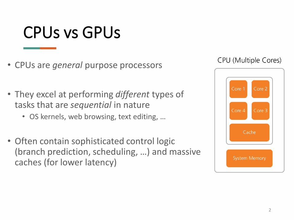
CPUs vs GPUs
• CPUs are general purpose processors
• They excel at performing different types of tasks that are sequential in nature• OS kernels, web browsing, text editing, …
• Often contain sophisticated control logic (branch prediction, scheduling, …) and massive caches (for lower latency)
2
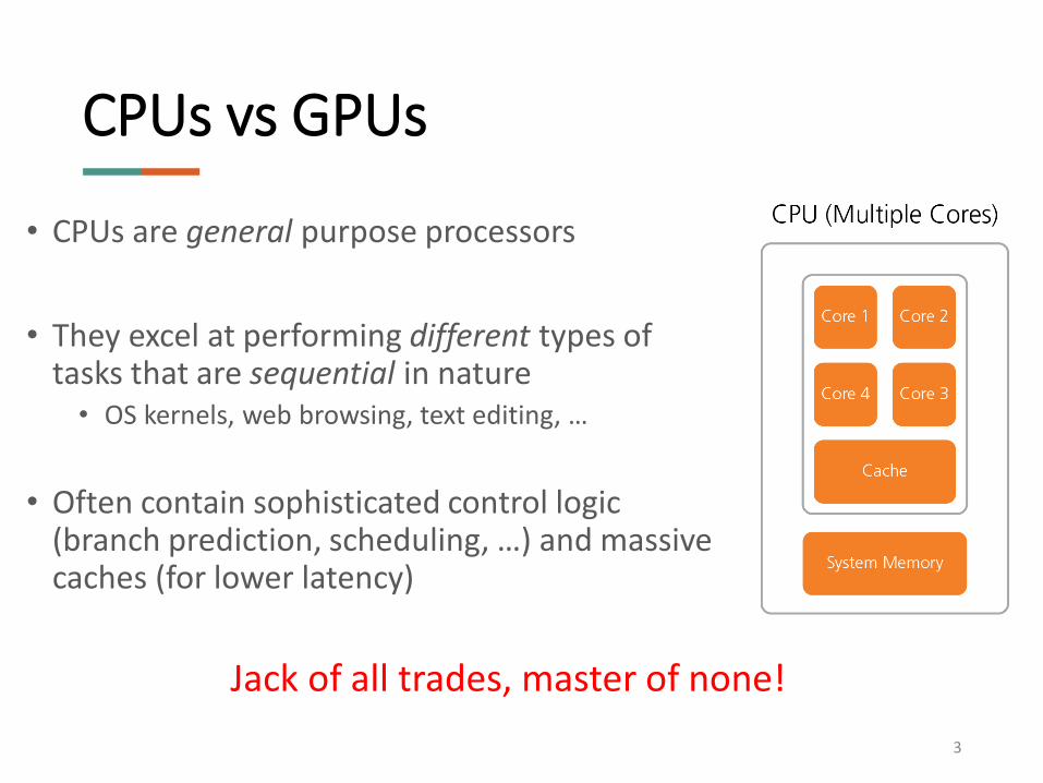
CPUs vs GPUs
• CPUs are general purpose processors
• They excel at performing different types of tasks that are sequential in nature• OS kernels, web browsing, text editing, …
• Often contain sophisticated control logic (branch prediction, scheduling, …) and massive caches (for lower latency)
Jack of all trades, master of none!
3
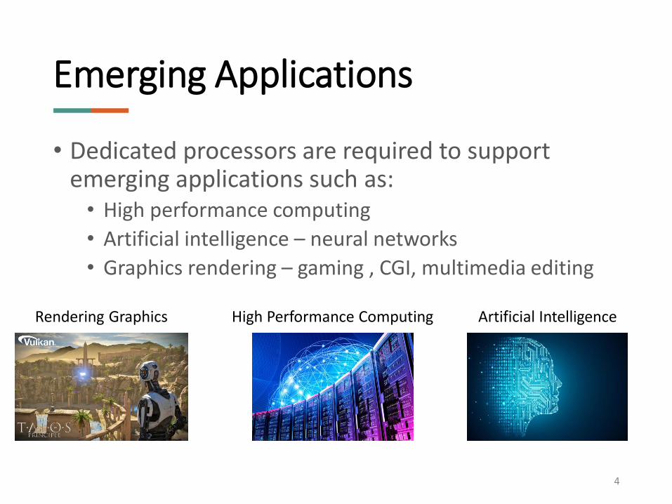
Emerging Applications
• Dedicated processors are required to support emerging applications such as:• High performance computing
• Artificial intelligence – neural networks
• Graphics rendering – gaming , CGI, multimedia editing
High Performance ComputingRendering Graphics Artificial Intelligence
4
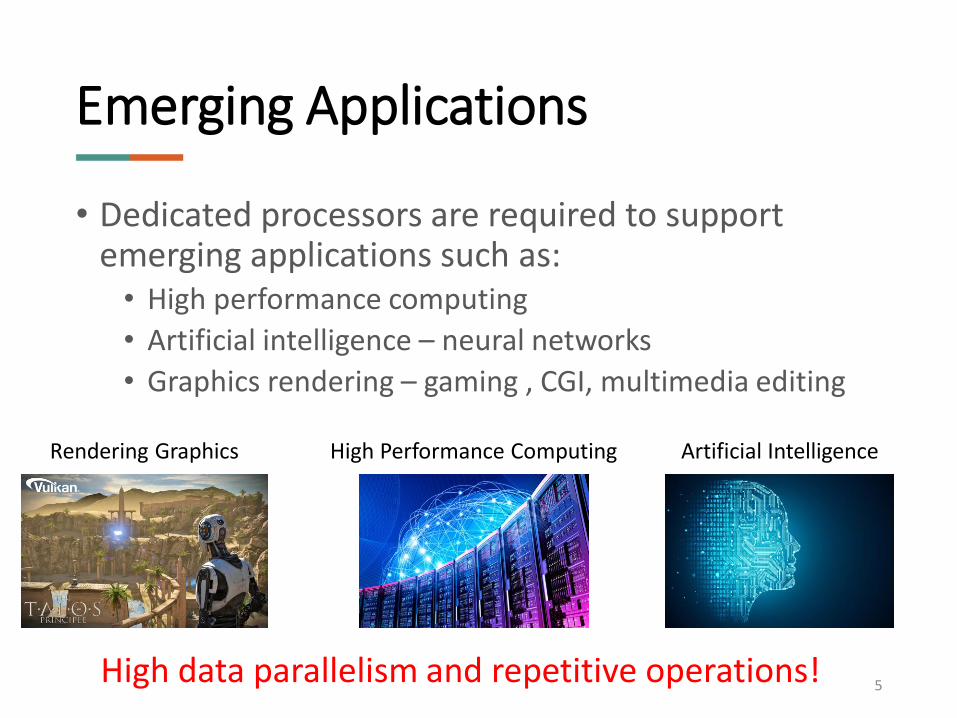
Emerging Applications
• Dedicated processors are required to support emerging applications such as:• High performance computing
• Artificial intelligence – neural networks
• Graphics rendering – gaming , CGI, multimedia editing
High Performance ComputingRendering Graphics Artificial Intelligence
High data parallelism and repetitive operations!5
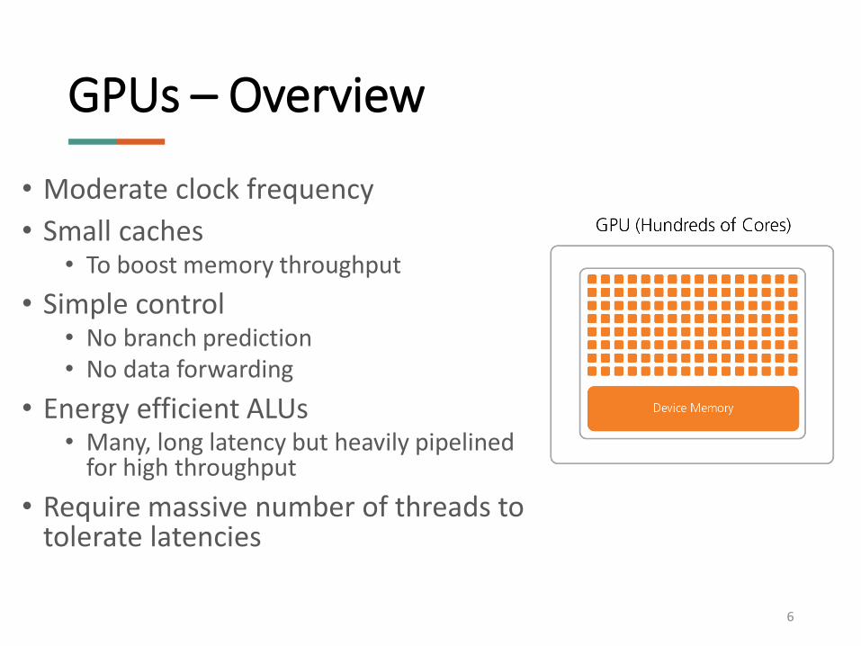
GPUs – Overview
• Moderate clock frequency
• Small caches• To boost memory throughput
• Simple control• No branch prediction• No data forwarding
• Energy efficient ALUs• Many, long latency but heavily pipelined
for high throughput
• Require massive number of threads to tolerate latencies
6
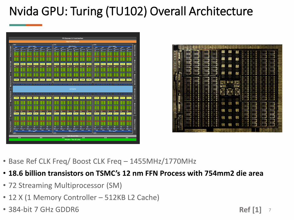
Nvida GPU: Turing (TU102) Overall Architecture
• Base Ref CLK Freq/ Boost CLK Freq – 1455MHz/1770MHz
• 18.6 billion transistors on TSMC’s 12 nm FFN Process with 754mm2 die area
• 72 Streaming Multiprocessor (SM)
• 12 X (1 Memory Controller – 512KB L2 Cache)
• 384-bit 7 GHz GDDR6 7Ref [1]
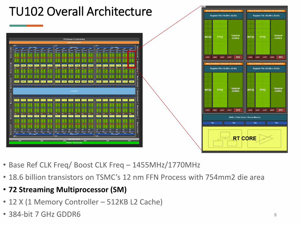
TU102 Overall Architecture
• Base Ref CLK Freq/ Boost CLK Freq – 1455MHz/1770MHz
• 18.6 billion transistors on TSMC’s 12 nm FFN Process with 754mm2 die area
• 72 Streaming Multiprocessor (SM)
• 12 X (1 Memory Controller – 512KB L2 Cache)
• 384-bit 7 GHz GDDR6 8
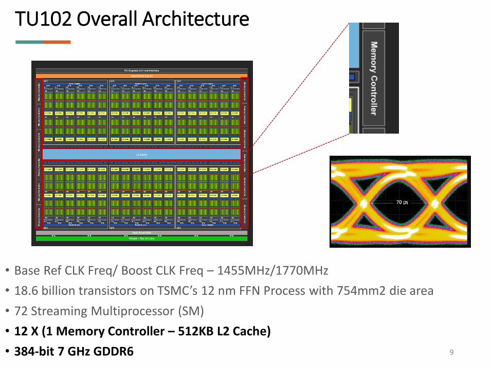
TU102 Overall Architecture
• Base Ref CLK Freq/ Boost CLK Freq – 1455MHz/1770MHz
• 18.6 billion transistors on TSMC’s 12 nm FFN Process with 754mm2 die area
• 72 Streaming Multiprocessor (SM)
• 12 X (1 Memory Controller – 512KB L2 Cache)
• 384-bit 7 GHz GDDR6 9
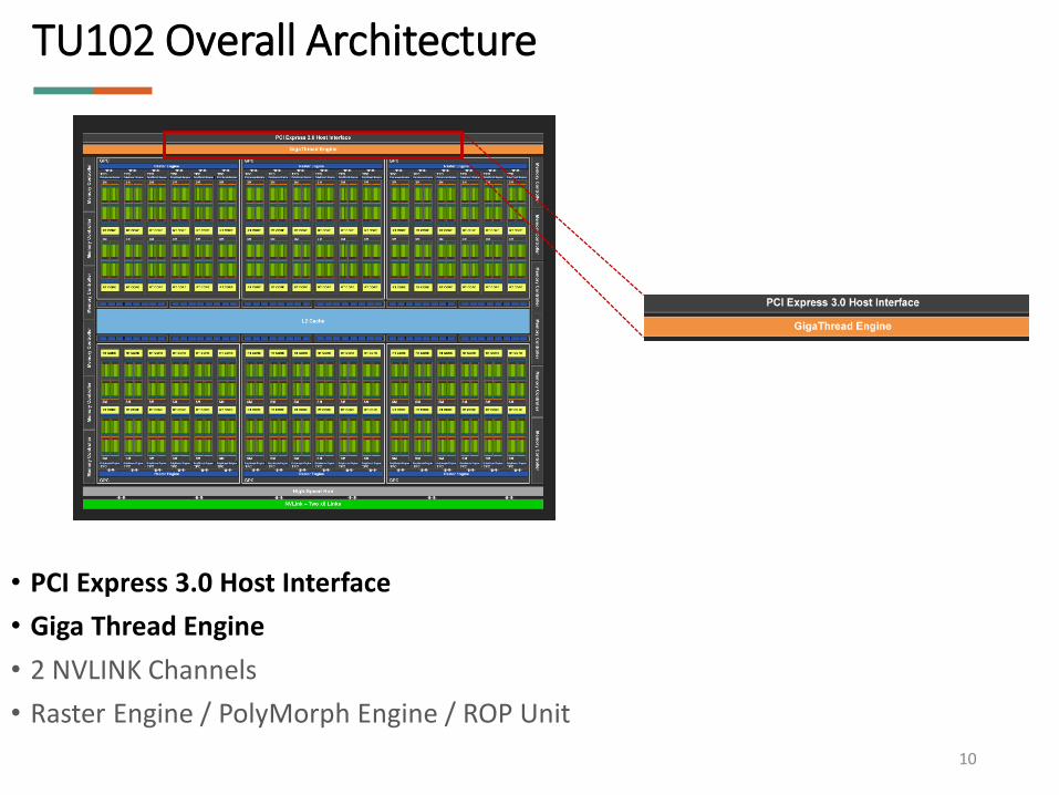
• PCI Express 3.0 Host Interface
• Giga Thread Engine
• 2 NVLINK Channels
• Raster Engine / PolyMorph Engine / ROP Unit
TU102 Overall Architecture
10
TU102 Overall Architecture
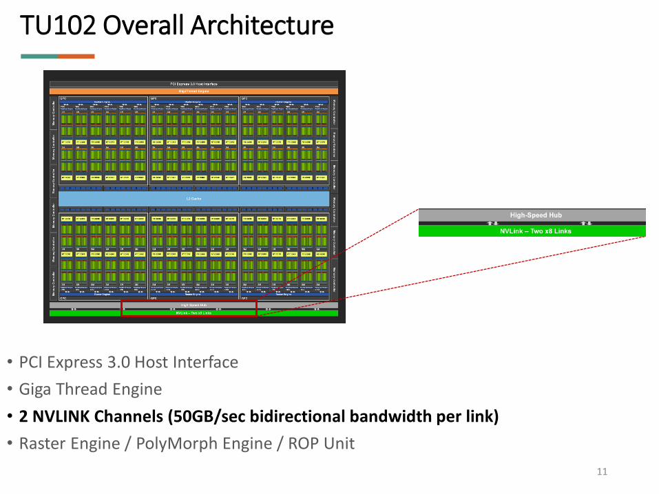
• PCI Express 3.0 Host Interface
• Giga Thread Engine
• 2 NVLINK Channels (50GB/sec bidirectional bandwidth per link)
• Raster Engine / PolyMorph Engine / ROP Unit
11
TU102 Overall Architecture
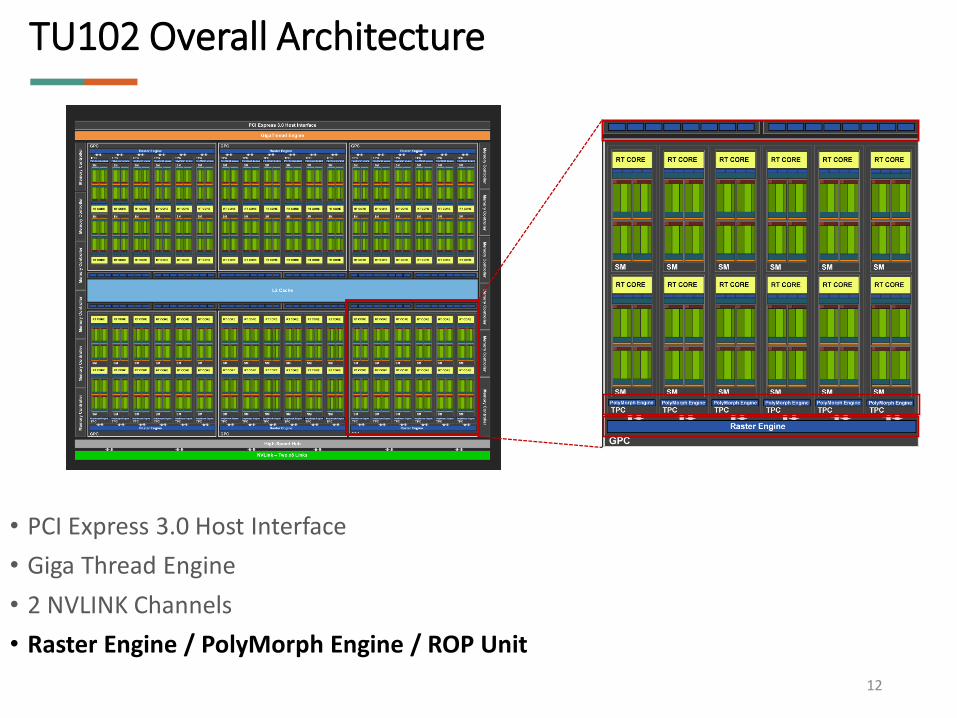
• PCI Express 3.0 Host Interface
• Giga Thread Engine
• 2 NVLINK Channels
• Raster Engine / PolyMorph Engine / ROP Unit
12
13
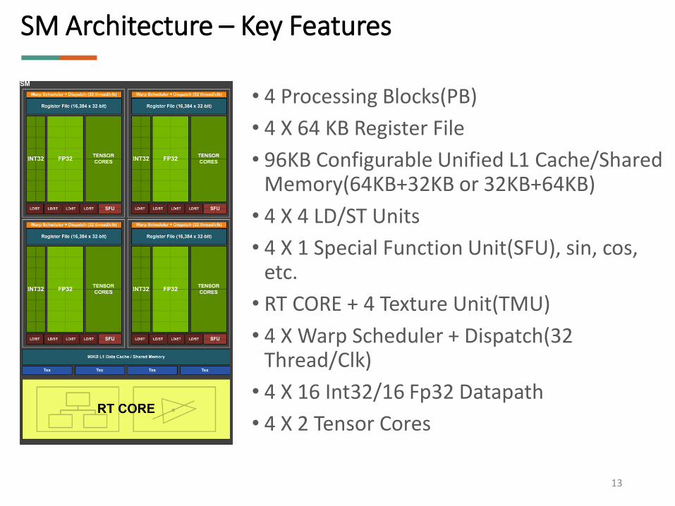
SM Architecture – Key Features
• 4 Processing Blocks(PB)
• 4 X 64 KB Register File
• 96KB Configurable Unified L1 Cache/Shared Memory(64KB+32KB or 32KB+64KB)
• 4 X 4 LD/ST Units
• 4 X 1 Special Function Unit(SFU), sin, cos, etc.
• RT CORE + 4 Texture Unit(TMU)
• 4 X Warp Scheduler + Dispatch(32 Thread/Clk)
• 4 X 16 Int32/16 Fp32 Datapath
• 4 X 2 Tensor Cores
14
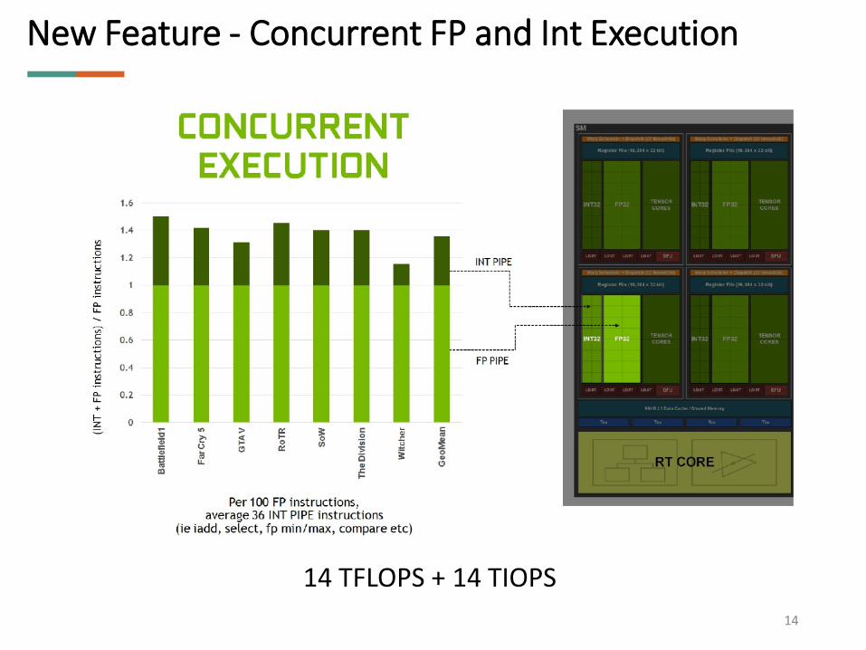
New Feature - Concurrent FP and Int Execution
14 TFLOPS + 14 TIOPS
15
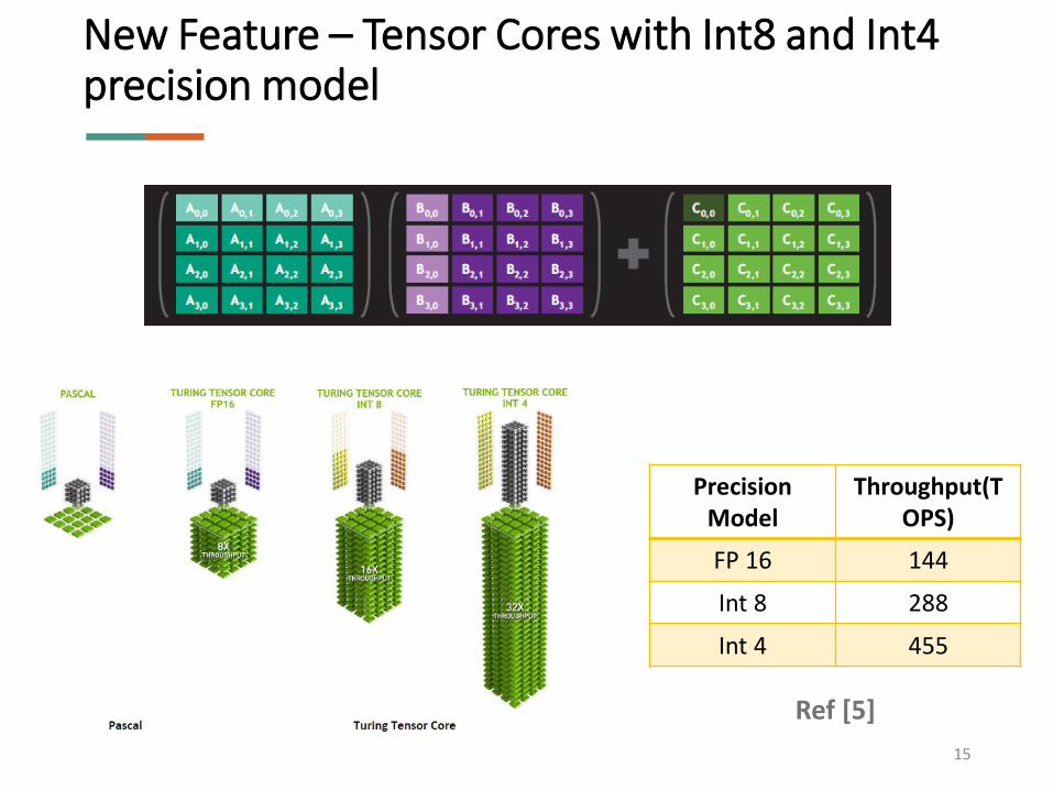
Precision Model
Throughput(TOPS)
FP 16 144
Int 8 288
Int 4 455
New Feature – Tensor Cores with Int8 and Int4 precision model
Ref [5]
16
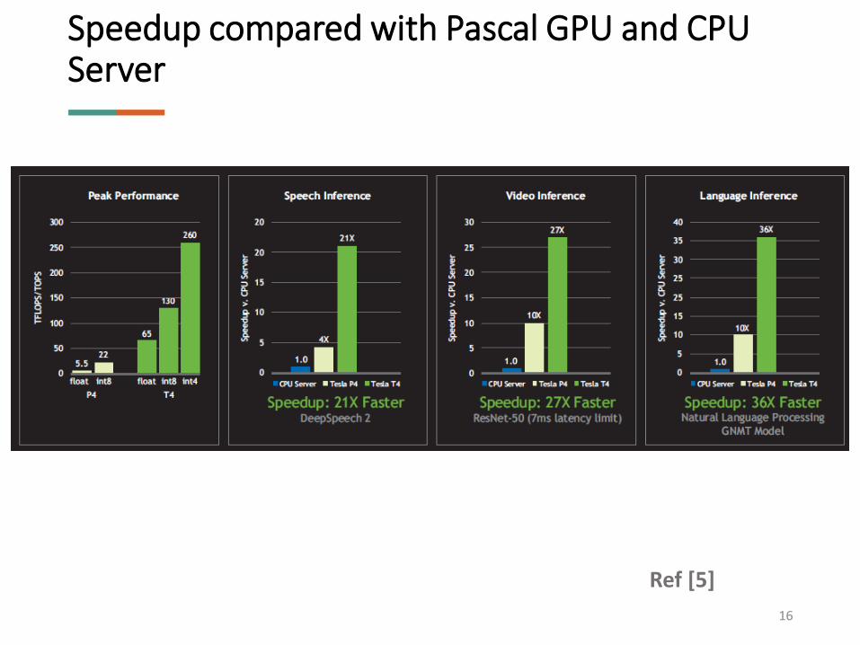
Speedup compared with Pascal GPU and CPU Server
Ref [5]
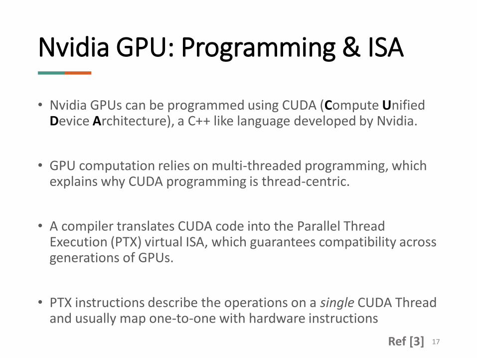
Nvidia GPU: Programming & ISA
• Nvidia GPUs can be programmed using CUDA (Compute Unified Device Architecture), a C++ like language developed by Nvidia.
• GPU computation relies on multi-threaded programming, which explains why CUDA programming is thread-centric.
• A compiler translates CUDA code into the Parallel Thread Execution (PTX) virtual ISA, which guarantees compatibility across generations of GPUs.
• PTX instructions describe the operations on a single CUDA Thread and usually map one-to-one with hardware instructions
Ref [3] 17
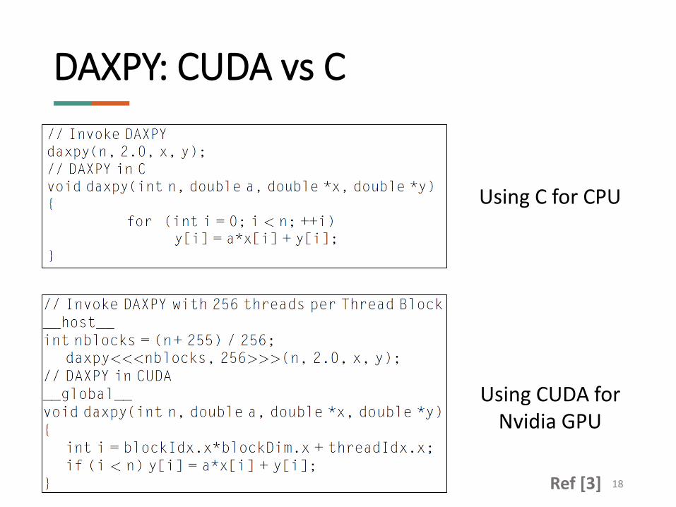
DAXPY: CUDA vs C
Using C for CPU
Using CUDA for Nvidia GPU
18Ref [3]
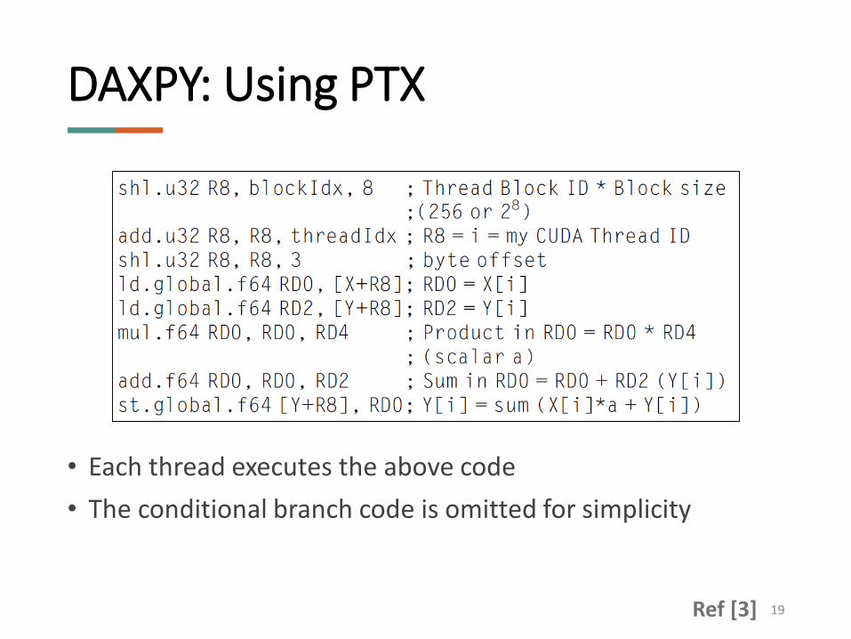
DAXPY: Using PTX
• Each thread executes the above code
• The conditional branch code is omitted for simplicity
19Ref [3]
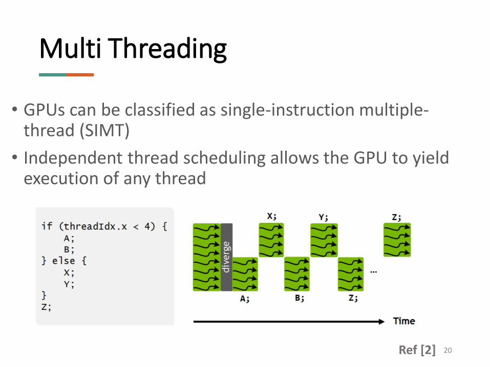
Multi Threading
• GPUs can be classified as single-instruction multiple-thread (SIMT)
• Independent thread scheduling allows the GPU to yield execution of any thread
20Ref [2]
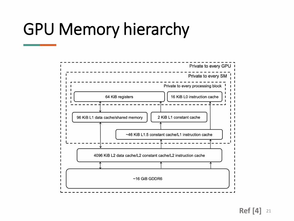
GPU Memory hierarchy
21Ref [4]
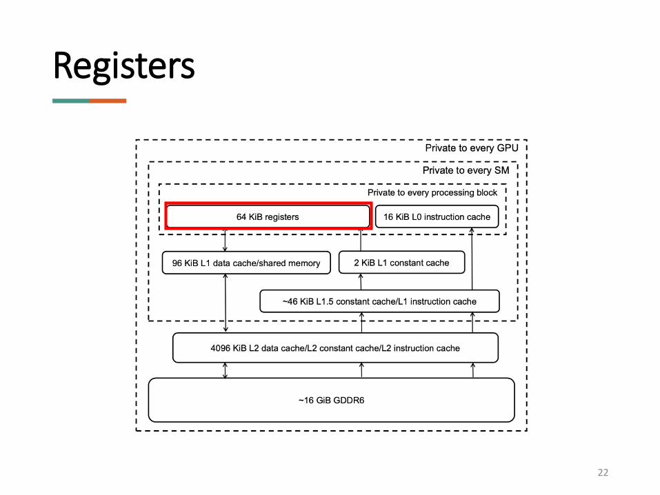
Registers
22
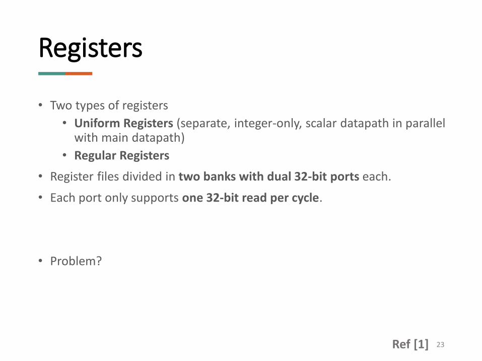
• Two types of registers
• Uniform Registers (separate, integer-only, scalar datapath in parallel with main datapath)
• Regular Registers
• Register files divided in two banks with dual 32-bit ports each.
• Each port only supports one 32-bit read per cycle.
• Problem?
Registers
23Ref [1]
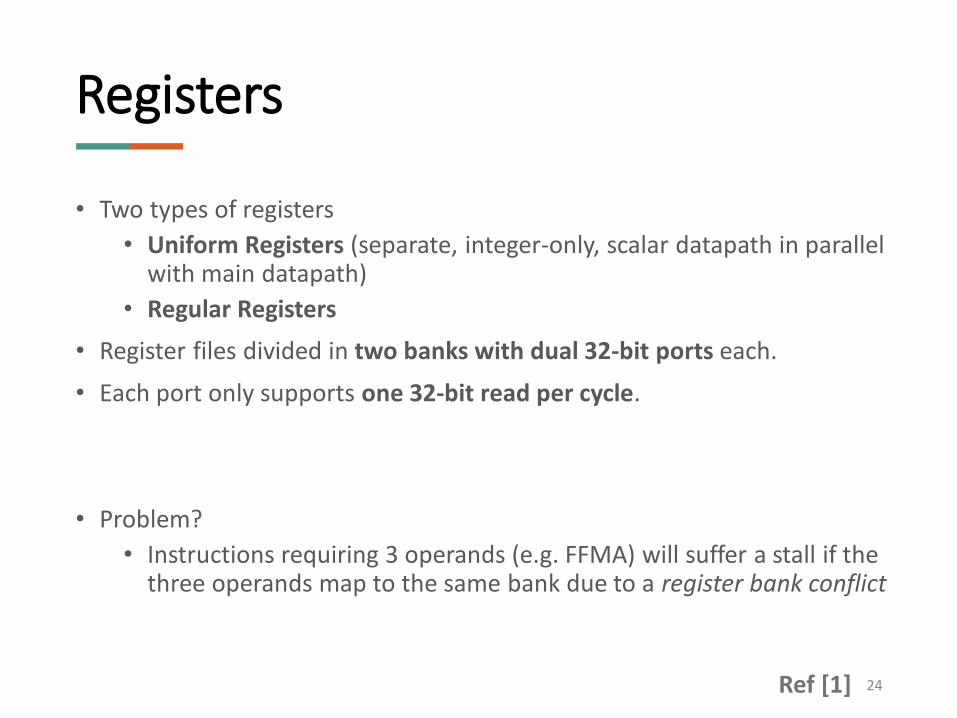
• Two types of registers
• Uniform Registers (separate, integer-only, scalar datapath in parallel with main datapath)
• Regular Registers
• Register files divided in two banks with dual 32-bit ports each.
• Each port only supports one 32-bit read per cycle.
• Problem?
• Instructions requiring 3 operands (e.g. FFMA) will suffer a stall if the three operands map to the same bank due to a register bank conflict
Registers
24Ref [1]
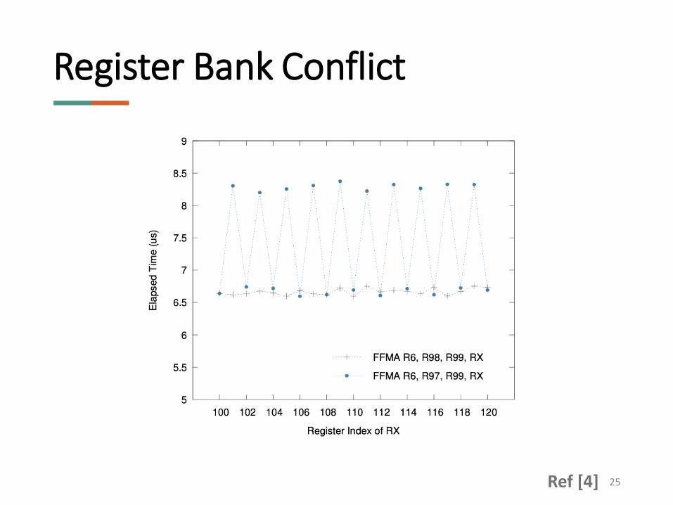
Register Bank Conflict
25Ref [4]
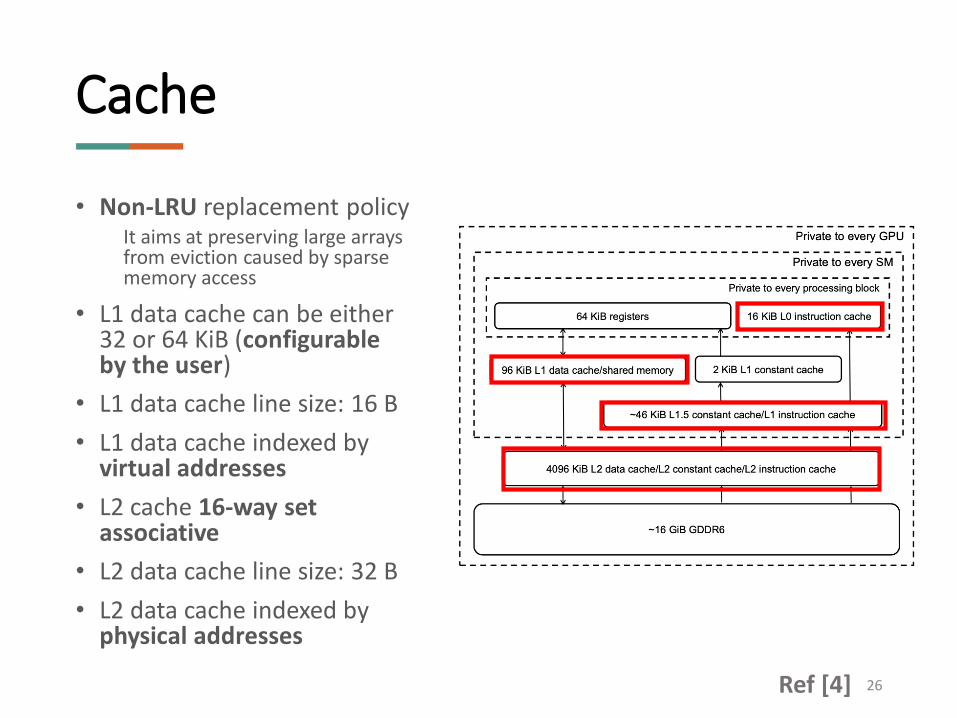
• Non-LRU replacement policyIt aims at preserving large arrays from eviction caused by sparse memory access
• L1 data cache can be either 32 or 64 KiB (configurable by the user)
• L1 data cache line size: 16 B
• L1 data cache indexed by virtual addresses
• L2 cache 16-way set associative
• L2 data cache line size: 32 B
• L2 data cache indexed by physical addresses
Cache
26Ref [4]
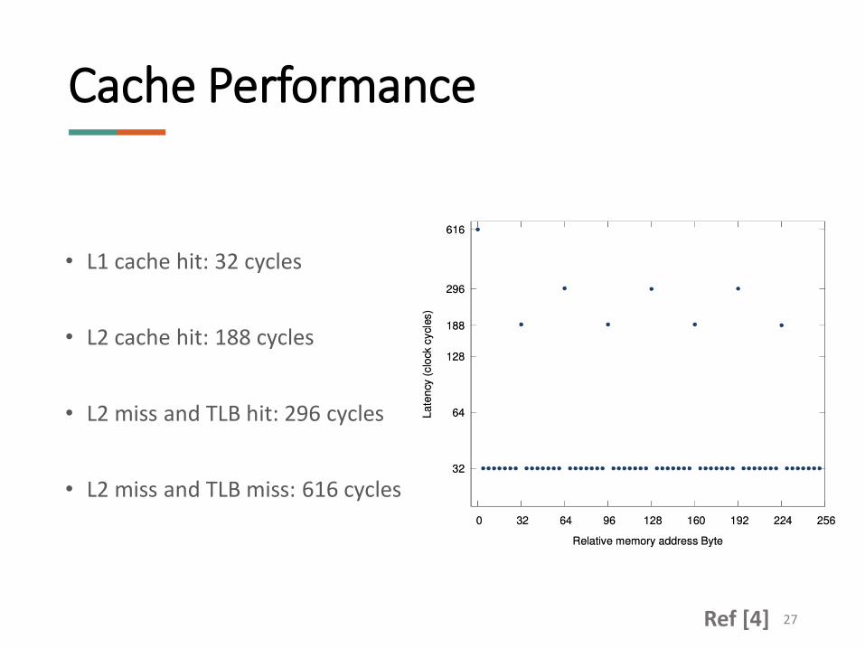
• L1 cache hit: 32 cycles
• L2 cache hit: 188 cycles
• L2 miss and TLB hit: 296 cycles
• L2 miss and TLB miss: 616 cycles
Cache Performance
27Ref [4]
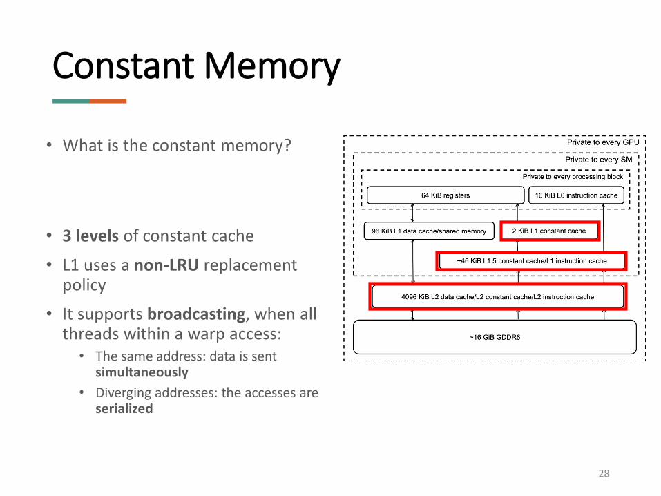
• What is the constant memory?
• 3 levels of constant cache
• L1 uses a non-LRU replacement policy
• It supports broadcasting, when all threads within a warp access:
• The same address: data is sent simultaneously
• Diverging addresses: the accesses are serialized
Constant Memory
28
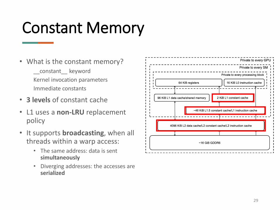
• What is the constant memory?__constant__ keyword
Kernel invocation parameters
Immediate constants
• 3 levels of constant cache
• L1 uses a non-LRU replacement policy
• It supports broadcasting, when all threads within a warp access:
• The same address: data is sent simultaneously
• Diverging addresses: the accesses are serialized
Constant Memory
29
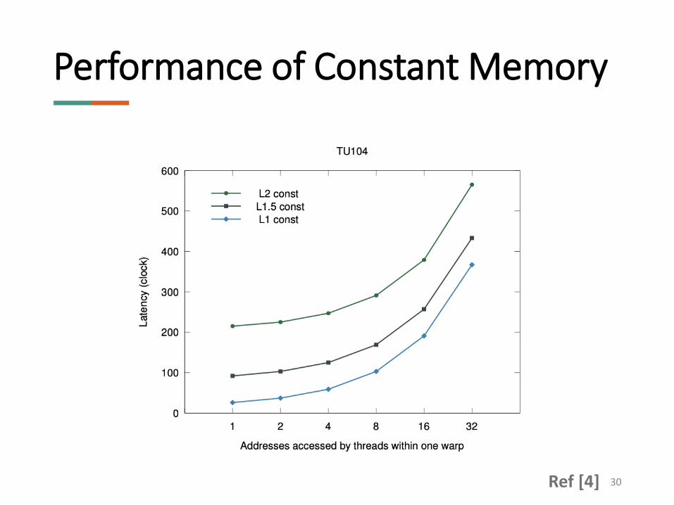
Performance of Constant Memory
30Ref [4]
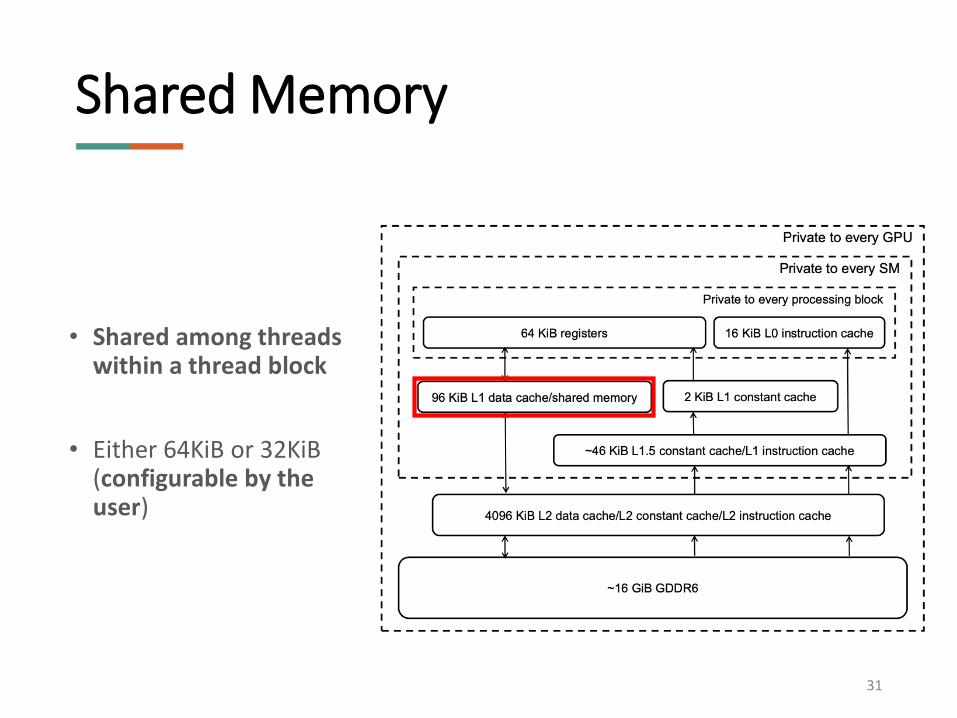
• Shared among threads within a thread block
• Either 64KiB or 32KiB (configurable by the user)
Shared Memory
31
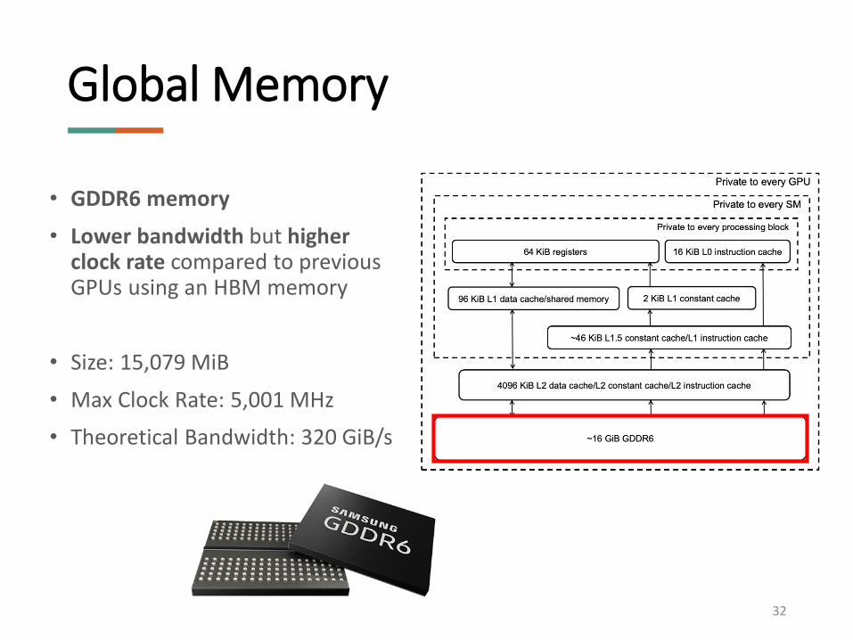
• GDDR6 memory
• Lower bandwidth but higher clock rate compared to previous GPUs using an HBM memory
• Size: 15,079 MiB
• Max Clock Rate: 5,001 MHz
• Theoretical Bandwidth: 320 GiB/s
Global Memory
32
• [1] Nvida Turing GPU Architecture: https://www.nvidia.com/content/dam/en-zz/Solutions/design-visualization/technologies/turing-architecture/NVIDIA-Turing-Architecture-Whitepaper.pdf
• [2] Nvida Tesla V100 (Volta) GPU Architecture: https://images.nvidia.com/content/volta-architecture/pdf/volta-architecture-whitepaper.pdf
• [3] Hennessy, John L., and David A. Patterson. Computer architecture: a quantitative approach. 6th edition.
• [4] Jia, Zhe, et al. "Dissecting the NVidia Turing T4 GPU via Microbenchmarking." arXiv preprint arXiv:1903.07486 (2019).
• [5] Burgess, John. "RTX ON–The NVIDIA TURING GPU." 2019 IEEE Hot Chips 31 Symposium (HCS). IEEE, 2019.
References
33