Embed Size (px)
Citation preview
Hard disk drive specificationsHitachi Microdrive™with CF+ Type II interface
Models 4GB 3K4-4 HMS360404D5CF00 2GB 3K4-2 HMS360402D5CF00
Revision 0.4 17 Oct. 2003
Hitachi Global Storage Technologies storage products
Hard disk drive specfication for Hitachi MicrodriveTM 3K4 Subject to change
1
S14R-8897-04 Publication #E001
Hitachi Global Storage Technologies storage products
Hard disk drive specfication for Hitachi MicrodriveTM 3K4 Subject to change
2
Hitachi Global Storage Technologies storage products
Hard disk drive specfication for Hitachi MicrodriveTM 3K4 Subject to change
3
Hard disk drive specifications
Hitachi Microdrive™with CF+ Type II interface
Models 4GB 3K4-4 HMS360404D5CF00 2GB 3K4-2 HMS360402D5CF00
Revision 0.4 17 Oct, 2003
S14R-8897-04 Publication #E001
Hitachi Global Storage Technologies storage products
Hard disk drive specfication for Hitachi MicrodriveTM 3K4 Subject to change
4
1st Revision (Rev 0.1) Sxxx-xxxx-xx (Jul. 14, 2003) Preliminary2nd Revision (Rev 0.2) Sxxx-xxxx-xx (Aug. 20, 2003) Preliminary - Power / zone format 3rd Revision (Rev 0.3) Sxxx-xxxx-xx (Oct. 10, 2003) Preliminary - Peak power / power rising time 4th Revision (Rev 0.4) S14R-8897-04 (Oct. 17, 2003)
The following paragraph does not apply to the United Kingdom or any country where such provisionsare inconsistent with local law: HITACHI GLOBAL STORAGE TECHINOLOGIES PROVIDES THISPUBLICATION "AS IS" WITHOUT WARRANTY OF ANY KIND, EITHER EXPRESS OR IMPLIED, IN-CLUDING,BUT NOT LIMITED TO, THE IMPLIED WARRANTIES OF MERCHANTABILITY OR FIT-NESS FOR A PARTICULAR PURPOSE. Some states do not allow disclaimer or express or implied warrantiesin certain transactions, therefore, this statement may not apply to you.
This publication could include technical inaccuracies or typographical errors. Changes are periodically made totheinformation herein; these changes will be incorporated in new editions of the publication. HGST may makeimprovements and/or changes in the product(s) and/or the program(s) described in this publication at any time.
It is possible that this publication may contain reference to, or information about, HGST products (machinesand programs), programming, or services that are not announced in your country. Such references orinformation must not be construed to mean that HGST intends to announce such HGST products, programming,or services in your country.
Technical information about this product is available by contacting a local HGST representative or
http://www.hgst.com
HGST may have patents or pending patent applications covering subject matter in this document. Thefurnishing of this document does not give you any license to these patents.
(C) Copyright Hitachi Global Storage Technologies
Note to U.S. Government Users — Documentation related to restricted rights — Use, duplication or disclosureis subject to restrictions set forth in GSA ADP Schedule Contract with HGST.
Hitachi Global Storage Technologies storage products
Hard disk drive specfication for Hitachi MicrodriveTM 3K4 Subject to change
5
Table of contents
327.5 Mechanical specifications ................................... .......317.4.2 Nonrecoverable errors ................................ .......317.4.1 Recoverable errors ................................... .......317.4 Error rates .............................................. .......307.3.4 Preventive maintenance ............................... .......307.3.3 Life .............................................. .......307.3.2 Warranty .......................................... .......307.3.1 Load/unload cycles ................................... .......307.3 Reliability ............................................... .......307.2 DC power requirements .................................... .......297.1.3 Magnetic fields ...................................... .......297.1.2 Conductive noise .................................... .......297.1.1 Radiation noise ..................................... .......287.1.1 Temperature and humidity ............................. .......287.1 Environment ............................................ .......287.0 Specification ........................................... .......266.0 File organization ........................................ .......255.7.3 Recovered read errors ................................ .......255.7.2 Nonrecovered read errors ............................. .......255.7.1 Nonrecovered write errors .............................. .......255.7 Automatic reallocation ..................................... .......255.6 Error recovery ........................................... .......245.5 Data buffer test .......................................... .......245.4 WRITE safety ........................................... .......245.3 Equipment status ......................................... .......245.2 Write cache ............................................. .......245.1 Data loss at power off ...................................... .......245.0 Data integrity ........................................... .......234.3.3 Operating modes .................................... .......214.3.2 Mechanical positioning ................................ .......214.3.1 Command overhead .................................. .......214.3 Performance characteristics ................................. .......204.2 Data sheet ............................................. .......204.1 Formatted capacity ....................................... .......204.0 Fixed disk characteristics ................................. .......183.2 Head disk assembly ....................................... .......183.1 Control electronics ........................................ .......183.0 Fixed disk subsystem description .......................... .......16Part 1. Functional specification ................................ .......142.0 General features ........................................ .......131.3 Drive handling precautions .................................. .......121.2 Abbreviations ........................................... .......121.1 References ............................................. .......121.0 General ............................................... .......10List of figures ............................................. .......
Hitachi Global Storage Technologies storage products
Hard disk drive specfication for Hitachi MicrodriveTM 3K4 Subject to change
6
5711.2 Card configuration registers ................................ .......5511.1 PCMCIA memory spaces and configuration registers ............. .......5511 System interface ......................................... .......5410 Deviations from Standard ................................. .......539.1 Introduction ............................................. .......539 General ................................................. .......52Part 2. Interface specification ................................. .......508.14 Power on/off timing ...................................... .......498.13 True IDE Mode Ultra DMA Data Transfer Timing ................. .......488.12 True IDE Mode Multiword DMA Data Transfer Timing ............. .......478.11 True IDE Mode I/O Input (Read) Timing ....................... .......468.10 I/O Input (Write) timing .................................... .......458.9 I/O Input (Read) timing .................................... .......448.8 Attribute and Common Memory Read timing ..................... .......438.7 Common Memory Read timing ............................... .......428.6 Attribute Memory Read timing ............................... .......418.5 Interface logic signal levels ................................. .......408.4 Signal description ........................................ .......408.3 Signal definition ......................................... .......408.2 Interface connector ....................................... .......408.1 Cabling ................................................ .......408.0 Electrical interface specifications ........................... .......377.11 Packaging ............................................. .......377.10.8 Secondary circuit protection ........................... .......377.10.7 Environment ....................................... .......377.10.6 Safe handling ...................................... .......377.10.5 Flammability ....................................... .......377.10.4 German Safety Mark ................................. .......377.10.3 IEC compliance .................................... .......367.10.2 Canadian Standards Authority (CSA) approval .............. .......367.10.1 Underwriters Lab (UL) approval ......................... .......367.10 Safety ................................................ .......367.9.2 C-Tick Mark ........................................ .......367.9.1 CE Mark ........................................... .......367.9 Electromagnetic compatibility ................................ .......367.8 Identification labels ........................................ .......357.7.2 Discrete tone penalty ................................. .......347.7.1 Sound power level ................................... .......347.7 Acoustics ............................................... .......347.6.4 Nonoperating shock .................................. .......347.6.3 Operating shock ..................................... .......347.6.2 Nonoperating vibration ................................ .......337.6.1 Operating vibration ................................... .......337.6 Vibration and shock ....................................... .......337.5.5 Load/Unload mechanism .............................. .......337.5.4 Mounting orientation .................................. .......337.5.3 Connector ......................................... .......327.5.2 Mechanical dimensions ............................... .......327.5.1 Physical dimensions and weight ......................... .......
Hitachi Global Storage Technologies storage products
Hard disk drive specfication for Hitachi MicrodriveTM 3K4 Subject to change
7
8112.9 Reassign Function ....................................... .......8012.8 Write Cache Function ..................................... .......7912.7 Seek Overlap .......................................... .......7812.6.4 Transition Time ..................................... .......7812.6.3 Low Power Idle mode ................................ .......7712.6.2Active Idle mode ..................................... .......7712.6.1 Performance Idle mode ............................... .......
7712.6 Advanced Power Management (Adaptive Battery Life Extender 3)Feature ................................................... .......
7612.5.7 Initial Power Mode at Power On ......................... .......7612.5.6 Interface Capability for Power Modes ..................... .......7612.5.5 Status ............................................ .......7612.5.4 Standby timer ...................................... .......7512.5.3 STANDBY command completion timing ................... .......7512.5.2 Power Management Commands ........................ .......7512.5.1 Power Mode ....................................... .......7512.5 Power Management Feature ................................ .......7412.4.2 LBA Addressing Mode ................................ .......7412.4.1 Logical CHS Addressing Mode .......................... .......7412.4 Sector Addressing Mode .................................. .......7212.3.3 Required power-off sequence .......................... .......7212.3.2 Emergency unload .................................. .......7212.3.1 Load/Unload ....................................... .......7212.3 Power-off considerations .................................. .......7112.2 Diagnostic and Reset considerations .......................... .......7012.1.1 Register Initialization ................................. .......6912.1 Reset Response ........................................ .......6811.4.13 Status Register .................................... .......6711.4.12 Sector Number Register ............................. .......6711.4.11 Sector Count Register ............................... .......6711.4.10 Feature Register ................................... .......6611.4.9 Error Register ...................................... .......6611.4.8 Device/Head Register ................................ .......6511.4.7 Drive Address Register ............................... .......6511.4.6 Device Control Register .............................. .......6411.4.5 Data Register ...................................... .......6411.4.4 Cylinder Low Register ................................ .......6411.4.3 Cylinder High Register ............................... .......6411.4.2 Command Register .................................. .......6411.4.1 Alternate Status Register .............................. .......6411.4 CF-ATA Registers ....................................... .......6311.3.4 True IDE Mode addressing ............................ .......6211.3.3 Memory mapped addressing ........................... .......6111.3.2 Contiguous I/O mapped addressing ...................... .......6011.3.1 Primary or Secondary I/O mapped addressing .............. .......6011.3 CF-ATA Drive Register Set Definition and Protocol ............... .......5911.2.4 Socket and Copy Register (Offset 06h) .................... .......5911.2.3 Pin Replacement Register (Offset 04h) .................... .......5811.2.2 Card Configuration Status Register (Offset 02h) ............. .......5711.2.1 Configuration Option Register (Offset 00h) ................. .......
Hitachi Global Storage Technologies storage products
Hard disk drive specfication for Hitachi MicrodriveTM 3K4 Subject to change
8
14613.6 Card information structure ................................. ......14513.5 Error Posting ........................................... ......14413.4.37 Write Verify (3Ch: Vendor Specific) ..................... ......14313.4.36 Write Sector(s) without Erase (38h) ..................... ......14113.4.35 Write Sector(s) (30h/31h) ............................. ......14013.4.34 Write Multiple without Erase (CDh) ...................... ......13813.4.33 Write Multiple (C5h) ................................. ......13613.4.32 Write Long (32h/33h) ................................ ......13413.4.31 Write DMA (CAh/CBh) ............................... ......13313.4.30 Write Buffer (E8h) .................................. ......13213.4.29 Wear Level (F5h) .................................. ......13113.4.28 Translate Sector (87h) .............................. ......13013.4.27 Standby Immediate (E0h/94h) ......................... ......12913.4.26Standby (E2h/96h) .................................. ......12813.4.25 Sleep (E6h/99h) ................................... ......12713.4.24 Set Multiple (C6h) .................................. ......12513.4.23 Set Features (EFh) ................................. ......12413.4.22 Sense Condition (F0h : vendor specific) .................. ......12313.4.21 Seek (7Xh) ....................................... ......12213.4.20 Security Erase Prepare (F3h) .......................... ......12013.4.19 Request Sense (03h) ............................... ......11913.4.18 Recalibrate (1Xh) .................................. ......11713.4.17 Read Verify (40h/41h) ............................... ......11513.4.16 Read Sector(s) (20h/21h) ............................. ......11313.4.15 Read Multiple (C4h) ................................. ......11113.4.14 Read Long (22h/23h) ................................ ......10913.4.13 Read DMA(C8h/C9h) ................................ ......10813.4.12 Read Buffer (E4h) .................................. ......10713.4.11 Initialize Device Parameters (91h) ...................... ......10613.4.10 Idle Immediate (E1h/95h) ............................. ......10513.4.9 Idle (E3h/97h) ...................................... ......9913.4.8Identify Device (ECh) ................................. .......9813.4.7Format Unit (F7h: Vendor Specific) ....................... .......9513.4.6 Format Track (50h: Vendor Specific) ..................... .......9413.4.5 Flush Cache (E7h) .................................. .......9313.4.4 Erase Sectors (C0h) ................................. .......9213.4.3 Execute Device Diagnostics (90h) ....................... .......9113.4.2 Check Power Mode (E5h/98h) .......................... .......8813.4.1 Access Metadata Storage - B8h ......................... .......8713.4 DMA Data Transfer Commands ............................. .......8613.3 Non-Data Commands ..................................... .......8513.2 Data Out Commands ..................................... .......8313.1 Data In Commands ...................................... .......8212.10.1 Meatadata Storage Command Set ...................... .......8212.10 Metadata Storage Function ................................ .......8112.9.1 Auto Reassign Function ............................... .......
Hitachi Global Storage Technologies storage products
Hard disk drive specfication for Hitachi MicrodriveTM 3K4 Subject to change
9
List of figures
51Figure 35. Power On/Off timing diagram ........................... .......50Figure 34. Power On/Off timing data .............................. .......49Figure 33. Ultra DMA data transfer timing data ...................... .......48Figure 32. Multiword DMA data transfer timing data ................... .......47Figure 31. True IDE Mode IO Input (Read) timing diagram .............. .......47Figure 30. True IDE Mode IO Input (Read) timing data ................. .......46Figure 29. I/O Write timing diagram ............................... .......46Figure 28. I/O Write timing data ................................. .......45Figure 27. Common Memory Read Timing diagram ................... .......45Figure 26. Common Memory Read Timing data ...................... .......44Figure 25. Attribute and Common Memory Read timing ................ .......44Figure 24. Attribute and Common Memory Read timing data ............ .......43Figure 23. Common Memory Read timing .......................... .......42Figure 22. Attribute Memory Read timing diagram .................... .......42Figure 21. Attribute Memory Read timing data ....................... .......41Figure 20. Interface logic signal levels. ............................ .......40Figure 19. DC characteristics ................................... .......35Figure 18. Sound power levels .................................. .......34Figure 17. Random vibration PSD profile breakpoints (nonoperating) ...... .......33Figure 16. Random vibration ................................... .......32Figure 15. Mechanical outline of the drive .......................... .......32Figure 14. Physical dimensions and weight ......................... .......30Figure 13. DC power requirements. .............................. .......29Figure 12. Radiation noise ..................................... .......28Figure 11. Temperature and humidity specifications ................... .......26Figure 10. Cylinder allocation ................................... .......23Figure 9. Operating modes .................................... .......23Figure 8. Drive Ready Time ................................... .......22Figure 7. Latency Time ....................................... .......22Figure 6. Single track seek time ................................ .......22Figure 5. Full stroke seek time ................................. .......21Figure 4. Mechanical positioning performance ...................... .......21Figure 3. Performance parameters .............................. .......20Figure 2. Data sheet ........................................ .......20Figure 1. Formatted capacity .................................. .......
Hitachi Global Storage Technologies storage products
Hard disk drive specfication for Hitachi MicrodriveTM 3K4 Subject to change
10

This page intentionally left blank.
1.0 GeneralThis document describes the characteristics of 1.0-type 3600-RPM hard disk drive with a CF+ Type IIinterface and with capacities of 4 GB and 2 GB. This drive is the HGST Microdrive™ and is hereafterreferred to as "the drive". This document defines the hardware functional and interface specifications.The drive is available in the following models:
• 4GB 3K4-4 HMS360404D5CF00 • 2GB 3K4-2 HMS360402D5CF00
The major difference among 3K4-4 and 3K4-2 is the number of heads.
The specifications are subject to change without notice.
1.1 ReferencesCompact Flash Specification Version 1.4
1.2 Abbreviations
to be definedTBD
Machine Level ControlMLC
3K4-4/3K4-2Hitachi Microdrive™
3K4-4/3K4-2drive
1,000,000 bits per square millimeterMb/sq-mm
128 x 1 024 bytes128 KB
1,000,000,000 bytesGB
1,000,000 bytesMB
1,024 bytesKB
1,000,000 bits per secondMbps
1,000 bits per millimeterKbit/mm
Hitachi Global Storage Technologies storage products
Hard disk drive specfication for Hitachi MicrodriveTM 3K4 Subject to change
12
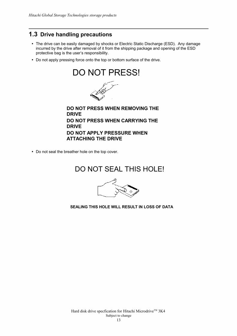
1.3 Drive handling precautionsThe drive can be easily damaged by shocks or Electric Static Discharge (ESD). Any damageincurred by the drive after removal of it from the shipping package and opening of the ESDprotective bag is the user’s responsibility.
Do not apply pressing force onto the top or bottom surface of the drive.
DO NOT PRESS!
DO NOT PRESS WHEN REMOVING THE DRIVEDO NOT PRESS WHEN CARRYING THE DRIVEDO NOT APPLY PRESSURE WHEN ATTACHING THE DRIVE
Do not seal the breather hole on the top cover.
DO NOT SEAL THIS HOLE!
SEALING THIS HOLE WILL RESULT IN LOSS OF DATA
Hitachi Global Storage Technologies storage products
Hard disk drive specfication for Hitachi MicrodriveTM 3K4 Subject to change
13
2.0 General featuresw Compact Flash Type-2 Card Compliance.
w 4.0GB and 2.0GB formatted capacity
w 512 bytes/sector
w CF+ Interface
w Integrated controller
w No-ID recording format
w ME2PR 120/126 coding
w Multi zone recording
w Enhanced ECC On-The-Fly
42.5 bytes Reed Solomon Code20 byte On-The-Fly correction
w 128kB cache (total buffer 320kB , upper 192KB is used for firmware)
w Fast data transfer rate
- Up to 16.7MB/sec at PIO mode 4
- Up to 16.7MB/sec at Multiword DMA mode 2 (True IDE Mode only) - Up to 33 MB/sec at Ultra DMA mode 2 (True IDE Mode only)
w Media data transfer rate 98 (outer zone / typical) - 57 (inner zone) Mbits/sec
w Average seek time 12 msec for read
w Closed -loop actuator servo (Embedded Sector Servo)
w True Track servo
w Rotary voice coil motor actuator
w Load/Unload mechanism
w Mechanical latch
w Adaptive power save control
w 1.0 sec Power on to ready
w Shock
– Non-operation : 19600 m/s2 / 1 ms (2000 G/1 ms) – Operation : 1960 m/s2 / 2 ms (200 G/2 ms)
Hitachi Global Storage Technologies storage products
Hard disk drive specfication for Hitachi MicrodriveTM 3K4 Subject to change
14

This page intentionally left blank.
Part 1. Functional specification
Hitachi Global Storage Technologies storage products
Hard disk drive specfication for Hitachi MicrodriveTM 3K4 Subject to change
16

This page intentionally left blank.
3.0 Fixed disk subsystem description
3.1 Control electronicsThe control electronics works with the following function:
Compact Flash Card Interface Protocol
Embedded Sector Servo
No-ID(TM) format
Multi zone recording
ME2PR 120/126 Code
ECC On-The-Fly
Enhanced Adaptive Battery Life Extender
3.2 Head disk assemblyThe following technologies are used in the drive:
Femto slider
Smooth glass disk
GMR head
Integrated Lead Suspension (ILS)
Load/Unload mechanism
Mechanical latch
Frame bumper
Hitachi Global Storage Technologies storage products
Hard disk drive specfication for Hitachi MicrodriveTM 3K4 Subject to change
18

This page intentionally left blank.
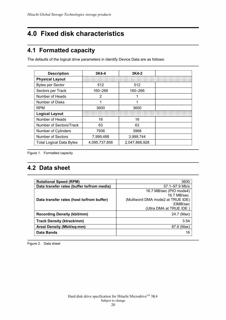
4.0 Fixed disk characteristics
4.1 Formatted capacityThe defaults of the logical drive parameters in Identify Device Data are as follows:
2,047,868,9284,095,737,856Total Logical Data Bytes3,999,7447,999,488Number of Sectors
39687936Number of Cylinders6363Number of Sectors/Track1616Number of Heads
Logical Layout36003600RPM
11Number of Disks12Number of Heads
160–266160–266Sectors per Track512512Bytes per Sector
Physical Layout3K4-23K4-4Description
Figure 1. Formatted capacity
4.2 Data sheet
16Data Bands87.6 (Max)Areal Density (Mbit/sq-mm)
3.54Track Density (ktrack/mm)
24.7 (Max)Recording Density (kbit/mm)
16.7 MB/sec (PIO mode4)16.7 MB/sec
(Multiword DMA mode2 at TRUE IDE)33MB/sec
(Ultra DMA at TRUE IDE )
Data transfer rates (host to/from buffer)
57.1–97.9 Mb/sData transfer rates (buffer to/from media)3600Rotational Speed (RPM)
Figure 2. Data sheet
Hitachi Global Storage Technologies storage products
Hard disk drive specfication for Hitachi MicrodriveTM 3K4 Subject to change
20
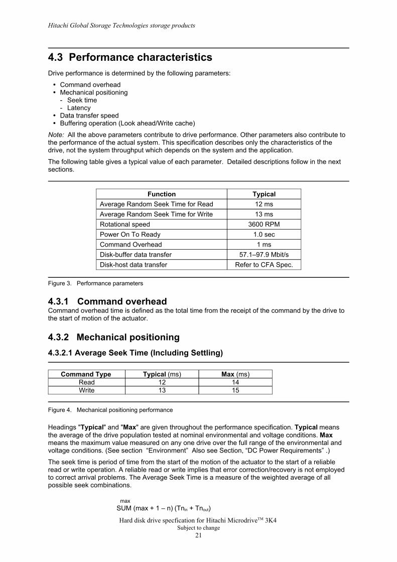
4.3 Performance characteristicsDrive performance is determined by the following parameters:
Command overheadMechanical positioning- Seek time- LatencyData transfer speedBuffering operation (Look ahead/Write cache)
Note: All the above parameters contribute to drive performance. Other parameters also contribute tothe performance of the actual system. This specification describes only the characteristics of thedrive, not the system throughput which depends on the system and the application.
The following table gives a typical value of each parameter. Detailed descriptions follow in the nextsections.
Refer to CFA Spec.Disk-host data transfer57.1–97.9 Mbit/sDisk-buffer data transfer
1 msCommand Overhead1.0 secPower On To Ready
3600 RPMRotational speed13 msAverage Random Seek Time for Write12 msAverage Random Seek Time for Read
TypicalFunction
Figure 3. Performance parameters
4.3.1 Command overheadCommand overhead time is defined as the total time from the receipt of the command by the drive tothe start of motion of the actuator.
4.3.2 Mechanical positioning4.3.2.1 Average Seek Time (Including Settling)
1513Write1412Read
Max (ms)Typical (ms)Command Type
Figure 4. Mechanical positioning performance
Headings "Typical" and "Max" are given throughout the performance specification. Typical meansthe average of the drive population tested at nominal environmental and voltage conditions. Maxmeans the maximum value measured on any one drive over the full range of the environmental andvoltage conditions. (See section “Environment” Also see Section, “DC Power Requirements” .)
The seek time is period of time from the start of the motion of the actuator to the start of a reliableread or write operation. A reliable read or write implies that error correction/recovery is not employedto correct arrival problems. The Average Seek Time is a measure of the weighted average of allpossible seek combinations.
max SUM (max + 1 – n) (Tnin + Tnout)
Hitachi Global Storage Technologies storage products
Hard disk drive specfication for Hitachi MicrodriveTM 3K4 Subject to change
21
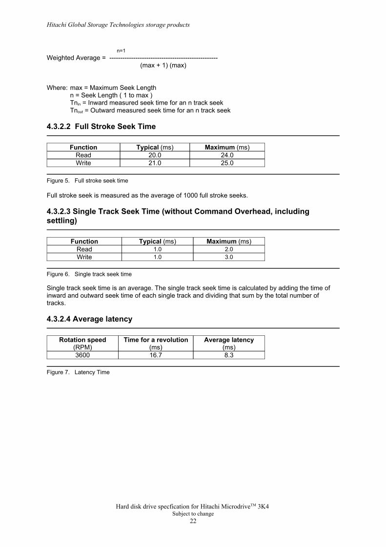
n=1Weighted Average = --------------------------------------------------
(max + 1) (max)
Where: max = Maximum Seek Lengthn = Seek Length ( 1 to max )Tnin = Inward measured seek time for an n track seekTnout = Outward measured seek time for an n track seek
4.3.2.2 Full Stroke Seek Time
25.021.0Write24.020.0Read
Maximum (ms)Typical (ms)Function
Figure 5. Full stroke seek time
Full stroke seek is measured as the average of 1000 full stroke seeks.
4.3.2.3 Single Track Seek Time (without Command Overhead, includingsettling)
3.01.0Write2.01.0Read
Maximum (ms)Typical (ms)Function
Figure 6. Single track seek time
Single track seek time is an average. The single track seek time is calculated by adding the time ofinward and outward seek time of each single track and dividing that sum by the total number oftracks.
4.3.2.4 Average latency
8.316.73600
Average latency(ms)
Time for a revolution(ms)
Rotation speed(RPM)
Figure 7. Latency Time
Hitachi Global Storage Technologies storage products
Hard disk drive specfication for Hitachi MicrodriveTM 3K4 Subject to change
22
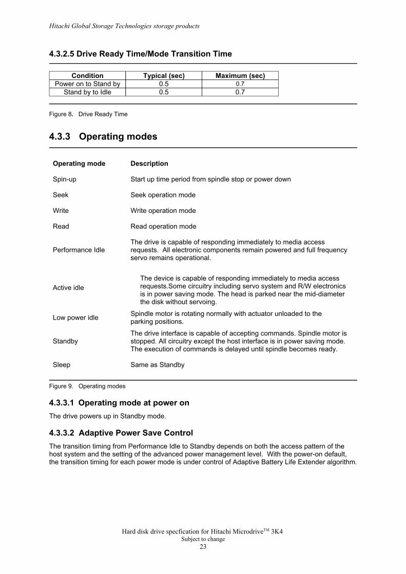
4.3.2.5 Drive Ready Time/Mode Transition Time
0.70.5Stand by to Idle0.70.5Power on to Stand by
Maximum (sec)Typical (sec)Condition
Figure 8. Drive Ready Time
4.3.3 Operating modes
Same as StandbySleep
The drive interface is capable of accepting commands. Spindle motor isstopped. All circuitry except the host interface is in power saving mode.The execution of commands is delayed until spindle becomes ready.
Standby
Spindle motor is rotating normally with actuator unloaded to theparking positions.Low power idle
The device is capable of responding immediately to media accessrequests.Some circuitry including servo system and R/W electronicsis in power saving mode. The head is parked near the mid-diameterthe disk without servoing.
Active idle
The drive is capable of responding immediately to media accessrequests. All electronic components remain powered and full frequencyservo remains operational.
Performance Idle
Read operation modeRead
Write operation modeWrite
Seek operation modeSeek
Start up time period from spindle stop or power downSpin-up
DescriptionOperating mode
Figure 9. Operating modes
4.3.3.1 Operating mode at power onThe drive powers up in Standby mode.
4.3.3.2 Adaptive Power Save ControlThe transition timing from Performance Idle to Standby depends on both the access pattern of thehost system and the setting of the advanced power management level. With the power-on default,the transition timing for each power mode is under control of Adaptive Battery Life Extender algorithm.
Hitachi Global Storage Technologies storage products
Hard disk drive specfication for Hitachi MicrodriveTM 3K4 Subject to change
23
5.0 Data integrity
5.1 Data loss at power offPower off during any operations except for write operation will not cause any data loss.
Power off during a write operation causes the loss of data received by the drive but not yet writtenonto the disk media.
There is a possibility that power off during a write operation might make a maximum of 1 sector ofdata unreadable. This state can be recovered by a rewrite operation.
5.2 Write cacheWhen write cache is enabled, there is a possibility that the write command completes before theactual disk write operation finishes. This means that there is a possibility that a power off eventmay occur even after a full write command finishes. This means that it is possible that even aftera write command completion a power off might cause the loss of the data which the drive hasreceived but not yet written onto the disk.
In order to prevent data loss, confirm the completion of the actual write operation prior to thepower off by issuing the Standby Immediate or Sleep command and confirming its completion.
The default state of the write cache at power-on is "OFF."
5.3 Equipment statusEquipment status is available to the host system any time the drive is not ready to read, write, orseek. This status normally exists at power-on time and will be maintained until the following conditionsare satisfied:
Access recalibration/tuning is complete.Spindle speed meets requirements for reliable operation.Self-check of drive is complete.
Appropriate error status is made available to the host system if either of the following conditions occurafter the drive has once become ready:
Spindle speed outside requirements for reliable operation.Occurrence of a Write Fault condition.
5.4 WRITE safetyThe drive ensures that the data is written onto the disk media properly. The following conditions aremonitored during a write operation. When one of those conditions exceeds the criteria, the writeoperation is terminated and automatic retry sequence will be invoked.
Head off trackExternal shockLow supply voltageSpindle speed toleranceHead open/short
5.5 Data buffer testThe data buffer is tested at Power-on-reset. The test consists of a write/read "00"x and "ff"x pattern oneach buffer position.
Hitachi Global Storage Technologies storage products
Hard disk drive specfication for Hitachi MicrodriveTM 3K4 Subject to change
24
5.6 Error recoveryErrors occurring on the drive are handled by the error recovery procedure.
Errors that are uncorrectable after application of the error recovery procedures are reported to thehost system as nonrecoverable errors.
5.7 Automatic reallocationThe sectors those show some errors may be reallocated automatically when specific conditions aremet. The drive does not report automatic reallocation to the host system. The conditions for automaticreallocation are described below.
5.7.1 Nonrecovered write errorsWhen a write operation cannot be completed after the Error Recovery Procedure (ERP) is fullycarried out, the sector(s) are reallocated to the spare location. An error is reported to the host systemonly when the write cache is disabled and the auto reallocation has failed.
5.7.2 Nonrecovered read errors
When a read operation has failed after defined ERP is fully carried out, a hard error is reported to thehost system. This location is registered internally as a candidate for the reallocation. When aregistered location is specified as a target of a write operation, a sequence of media verification isperformed automatically. When the result of this verification meets the criteria, this sector isreallocated.
5.7.3 Recovered read errors
When a read operation for a sector fails once and is then recovered at the specific ERP step, thissector is reallocated automatically. A media verification sequence may be run prior to the reallocationaccording to the predefined conditions.
Hitachi Global Storage Technologies storage products
Hard disk drive specfication for Hitachi MicrodriveTM 3K4 Subject to change
25
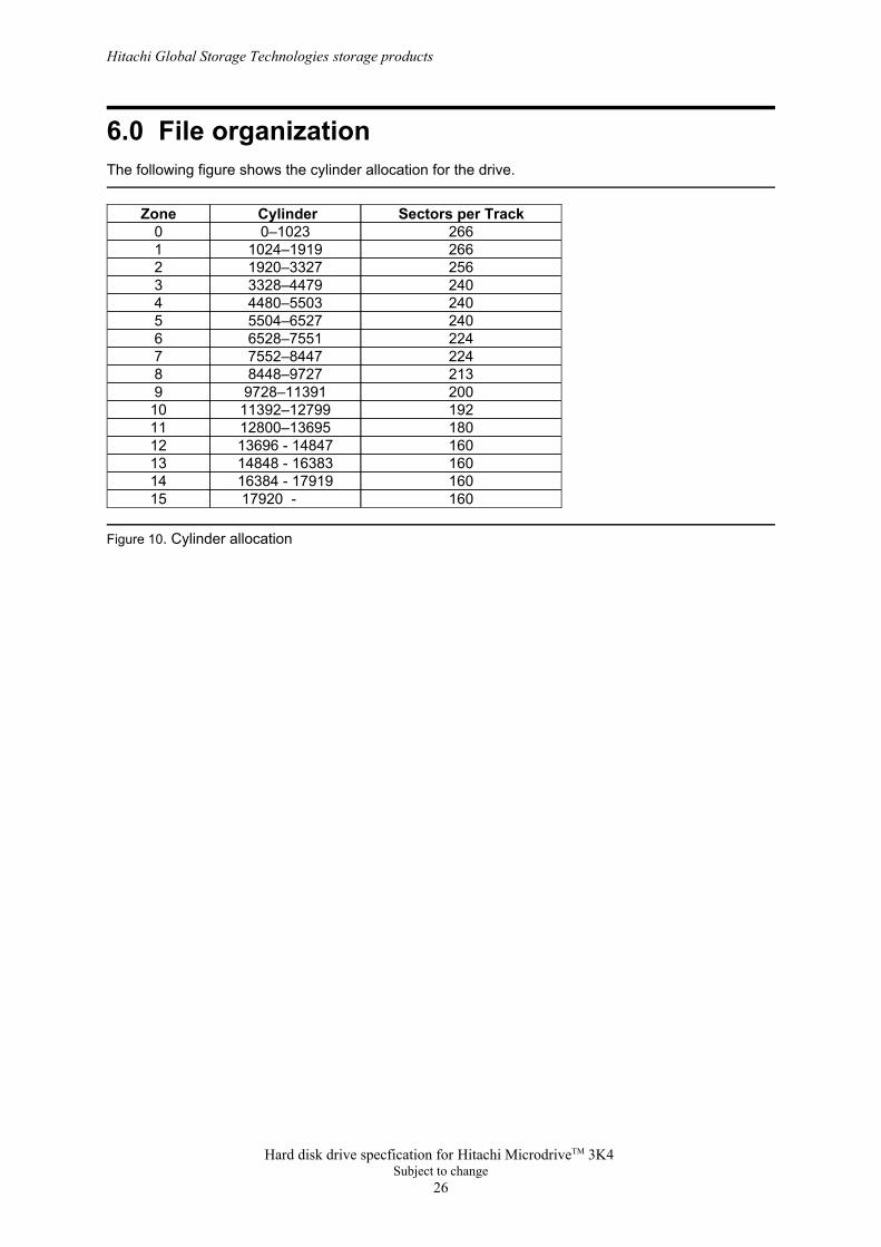
6.0 File organizationThe following figure shows the cylinder allocation for the drive.
16017920 - 1516016384 - 179191416014848 - 163831316013696 - 148471218012800–136951119211392–12799102009728–1139192138448–972782247552–844772246528–755162405504–652752404480–550342403328–447932561920–332722661024–191912660–10230
Sectors per Track CylinderZone
Figure 10. Cylinder allocation
Hitachi Global Storage Technologies storage products
Hard disk drive specfication for Hitachi MicrodriveTM 3K4 Subject to change
26

This page intentionally left blank.
7.0 Specification
7.1 Environment
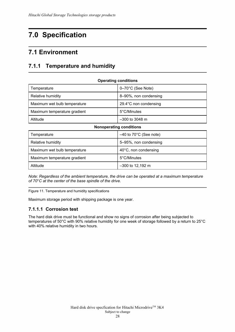
7.1.1 Temperature and humidity
–300 to 12,192 mAltitude
5°C/MinutesMaximum temperature gradient
40°C, non condensingMaximum wet bulb temperature
5–95%, non condensingRelative humidity
–40 to 70°C (See note)Temperature
Nonoperating conditions
–300 to 3048 mAltitude
5°C/MinutesMaximum temperature gradient
29.4°C non condensingMaximum wet bulb temperature
8–90%, non condensingRelative humidity
0–70°C (See Note)Temperature
Operating conditions
Note: Regardless of the ambient temperature, the drive can be operated at a maximum temperatureof 70°C at the center of the base spindle of the drive.
Figure 11. Temperature and humidity specifications
Maximum storage period with shipping package is one year.
7.1.1.1 Corrosion testThe hard disk drive must be functional and show no signs of corrosion after being subjected totemperatures of 50°C with 90% relative humidity for one week of storage followed by a return to 25°Cwith 40% relative humidity in two hours.
Hitachi Global Storage Technologies storage products
Hard disk drive specfication for Hitachi MicrodriveTM 3K4 Subject to change
28
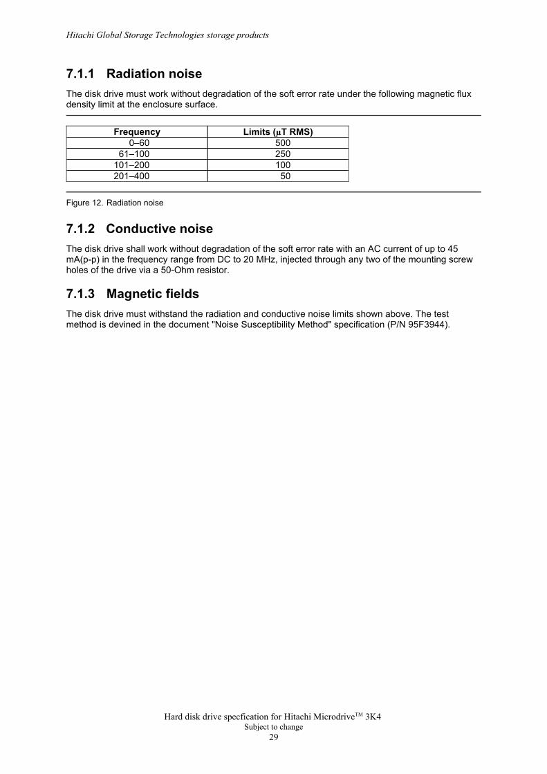
7.1.1 Radiation noiseThe disk drive must work without degradation of the soft error rate under the following magnetic fluxdensity limit at the enclosure surface.
50201–400100101–20025061–1005000–60
Limits (µT RMS)Frequency
Figure 12. Radiation noise
7.1.2 Conductive noiseThe disk drive shall work without degradation of the soft error rate with an AC current of up to 45mA(p-p) in the frequency range from DC to 20 MHz, injected through any two of the mounting screwholes of the drive via a 50-Ohm resistor.
7.1.3 Magnetic fieldsThe disk drive must withstand the radiation and conductive noise limits shown above. The testmethod is devined in the document "Noise Susceptibility Method" specification (P/N 95F3944).
Hitachi Global Storage Technologies storage products
Hard disk drive specfication for Hitachi MicrodriveTM 3K4 Subject to change
29
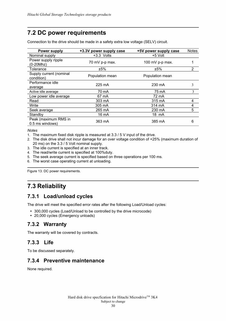
7.2 DC power requirementsConnection to the drive should be made in a safety extra low voltage (SELV) circuit.
6385 mA363 mAPeak (maximum RMS in0.5 ms windows)
18 mA 16 mAStandby5230 mA265 mASeek average4314 mA 305 mA Write4315 mA303 mARead
72 mA 67 mA Low power idle average 3 75 mA 70 mA Active idle average
3230 mA225 mAPerformance idleaverage
Population mean Population meanSupply current (nominalcondition)
2±5%±5%Tolerance
1100 mV p-p max.70 mV p-p max.Power supply ripple(0-20Mhz)
+5 Volt+3.3 VoltsNominal supplyNotes+5V power supply case+3.3V power supply casePower supply
Notes1. The maximum fixed disk ripple is measured at 3.3 / 5 V input of the drive.2. The disk drive shall not incur damage for an over voltage condition of +25% (maximum duration of
20 ms) on the 3.3 / 5 Volt nominal supply.3. The idle current is specified at an inner track.4. The read/write current is specified at 100%duty.5. The seek average current is specified based on three operations per 100 ms.6. The worst case operating current at unloading.
Figure 13. DC power requirements.
7.3 Reliability7.3.1 Load/unload cyclesThe drive will meet the specified error rates after the following Load/Unload cycles:
300,000 cycles (Load/Unload to be controlled by the drive microcode)20,000 cycles (Emergency unloads)
7.3.2 WarrantyThe warranty will be covered by contracts.
7.3.3 LifeTo be discussed separately.
7.3.4 Preventive maintenanceNone required.
Hitachi Global Storage Technologies storage products
Hard disk drive specfication for Hitachi MicrodriveTM 3K4 Subject to change
30
7.4 Error ratesError rates fall into two categories:
Recoverable errorsNonrecoverable errors
The following error rates assume that no attempts are made to read or write in areas alreadyidentified as being defective. The error rates are defined for the drive operating at the full range ofenvironmental conditions and are shown in section “Environment”. The voltage limits are shown insection “DC Power Requirements”.
7.4.1 Recoverable errorsA recoverable error is defined as an operation that failed the first time but succeeded in recoveringthe error when the drive error recovery procedure was invoked. ECC On-The-Fly, which is alwaysactive, is transparent to the system and is not counted as a recoverable error.
A typical drive shall have no more than one recoverable error per 100 million bits transferred (1 in 108)when operated at nominal voltage and environmental condition. The typical disk drive error raterepresents the geometric mean of the error rates of the total disk drive population. The size of thedrive population is 50 drives or more.
Each drive in the population shall have no more than one recoverable error per 10 million bitstransferred (1 in 107) when operated at full range of voltage and environmental conditions and theoperating vibration levels stated in, “Vibration and Shock” on page 0.
7.4.2 Nonrecoverable errors A nonrecoverable error is defined as an operation that failed and was not recovered by the fixed diskerror recovery procedure. No drive has more than one nonrecoverable error per 10 trillion bitstransferred (1 in 1013) when operated at the full range of voltage and environmental conditions.
Hitachi Global Storage Technologies storage products
Hard disk drive specfication for Hitachi MicrodriveTM 3K4 Subject to change
31
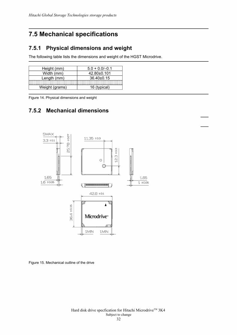
7.5 Mechanical specifications
7.5.1 Physical dimensions and weightThe following table lists the dimensions and weight of the HGST Microdrive.
16 (typical)Weight (grams)
36.40±0.15Length (mm)42.80±0.101Width (mm)
5.0 + 0.0/–0.1Height (mm)
Figure 14. Physical dimensions and weight
7.5.2 Mechanical dimensions
Figure 15. Mechanical outline of the drive
Hitachi Global Storage Technologies storage products
Hard disk drive specfication for Hitachi MicrodriveTM 3K4 Subject to change
32
7.5.3 ConnectorSee Section, “Interface Connector”.
7.5.4 Mounting orientationThe drive will operate in all axes (360°).
Performance and error rate will stay within specification limits if the drive is operated in the otherpermissible orientations from which it was formatted. Thus a drive formatted in a horizontal orientationis able to run vertically and vice versa.
Vibration test and shock test are to be conducted by mounting the drive to the test table using aspecial fixture.
7.5.5 Load/Unload mechanismThe head load/unload mechanism is provided to protect the disk during shipping, movement, orstorage.Upon power down, a head unload mechanism secures the heads at the unload position. See Section,“Nonoperating shock” for additional details.
7.6 Vibration and shockAll vibration and shock measurements in this section are for the drive without the mountingattachments for the systems. The input level is applied to the normal drive mounting points.
7.6.1 Operating vibrationThe drive will operate without a hard error while being subjected to the following vibration levels.
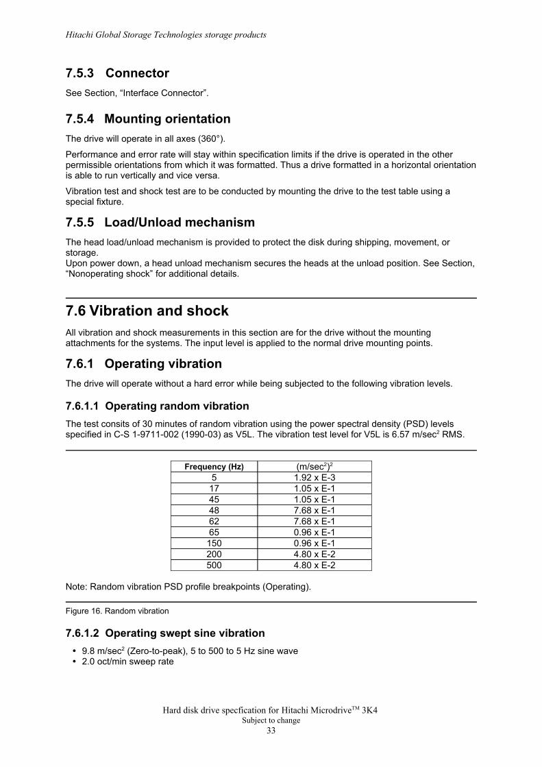
7.6.1.1 Operating random vibrationThe test consits of 30 minutes of random vibration using the power spectral density (PSD) levelsspecified in C-S 1-9711-002 (1990-03) as V5L. The vibration test level for V5L is 6.57 m/sec2 RMS.
4.80 x E-25004.80 x E-22000.96 x E-11500.96 x E-1657.68 x E-1627.68 x E-1481.05 x E-1451.05 x E-1171.92 x E-35(m/sec2)2Frequency (Hz)
Note: Random vibration PSD profile breakpoints (Operating).
Figure 16. Random vibration
7.6.1.2 Operating swept sine vibration9.8 m/sec2 (Zero-to-peak), 5 to 500 to 5 Hz sine wave2.0 oct/min sweep rate
Hitachi Global Storage Technologies storage products
Hard disk drive specfication for Hitachi MicrodriveTM 3K4 Subject to change
33
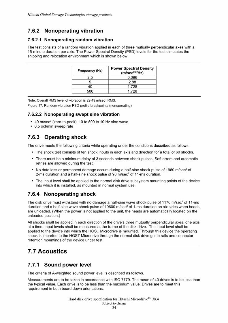
7.6.2 Nonoperating vibration7.6.2.1 Nonoperating random vibrationThe test consists of a random vibration applied in each of three mutually perpendicular axes with a15-minute duration per axis. The Power Spectral Density (PSD) levels for the test simulates theshipping and relocation environment which is shown below.
1.7285001.728402.8850.0962.5
Power Spectral Density(m/sec2)2/Hz)Frequency (Hz)
Note: Overall RMS level of vibration is 29.49 m/sec2 RMS.Figure 17. Random vibration PSD profile breakpoints (nonoperating)
7.6.2.2 Nonoperating swept sine vibration49 m/sec2 (zero-to-peak), 10 to 500 to 10 Hz sine wave0.5 oct/min sweep rate
7.6.3 Operating shockThe drive meets the following criteria while operating under the conditions described as follows:
The shock test consists of ten shock inputs in each axis and direction for a total of 60 shocks.
There must be a minimum delay of 3 seconds between shock pulses. Soft errors and automaticretries are allowed during the test.
No data loss or permanent damage occurs during a half-sine shock pulse of 1960 m/sec2 of2-ms duration and a half-sine shock pulse of 98 m/sec2 of 11-ms duration.
The input level shall be applied to the normal disk drive subsystem mounting points of the deviceinto which it is installed, as mounted in normal system use.
7.6.4 Nonoperating shockThe disk drive must withstand with no damage a half-sine wave shock pulse of 1176 m/sec2 of 11-msduration and a half-sine wave shock pulse of 19600 m/sec2 of 1-ms duration on six sides when headsare unloaded. (When the power is not applied to the unit, the heads are automatically located on theunloaded position.)
All shocks shall be applied in each direction of the drive’s three mutually perpendicular axes, one axisat a time. Input levels shall be measured at the frame of the disk drive. The input level shall beapplied to the device into which the HGST Microdrive is mounted. Through this device the operatingshock is imparted to the HGST Microdrive through the normal disk drive guide rails and connectorretention mountings of the device under test.
7.7 Acoustics
7.7.1 Sound power levelThe criteria of A-weighted sound power level is described as follows.
Measurements are to be taken in accordance with ISO 7779. The mean of 40 drives is to be less thanthe typical value. Each drive is to be less than the maximum value. Drives are to meet thisrequirement in both board down orientations.
Hitachi Global Storage Technologies storage products
Hard disk drive specfication for Hitachi MicrodriveTM 3K4 Subject to change
34
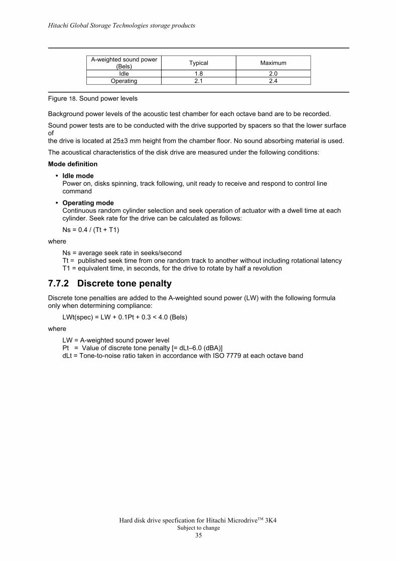
2.42.1Operating2.01.8Idle
MaximumTypicalA-weighted sound power(Bels)
Figure 18. Sound power levels
Background power levels of the acoustic test chamber for each octave band are to be recorded.
Sound power tests are to be conducted with the drive supported by spacers so that the lower surfaceofthe drive is located at 25±3 mm height from the chamber floor. No sound absorbing material is used.
The acoustical characteristics of the disk drive are measured under the following conditions:
Mode definition
Idle modePower on, disks spinning, track following, unit ready to receive and respond to control linecommand
Operating modeContinuous random cylinder selection and seek operation of actuator with a dwell time at eachcylinder. Seek rate for the drive can be calculated as follows:
Ns = 0.4 / (Tt + T1)
where
Ns = average seek rate in seeks/secondTt = published seek time from one random track to another without including rotational latencyT1 = equivalent time, in seconds, for the drive to rotate by half a revolution
7.7.2 Discrete tone penaltyDiscrete tone penalties are added to the A-weighted sound power (LW) with the following formulaonly when determining compliance:
LWt(spec) = LW + 0.1Pt + 0.3 < 4.0 (Bels)
where
LW = A-weighted sound power levelPt = Value of discrete tone penalty [= dLt–6.0 (dBA)]dLt = Tone-to-noise ratio taken in accordance with ISO 7779 at each octave band
Hitachi Global Storage Technologies storage products
Hard disk drive specfication for Hitachi MicrodriveTM 3K4 Subject to change
35
7.8 Identification labelsThe labels are affixed to every drive.
The top side of the label contains
Model namePart numberThe statement "Made by HGST"Country of originNotifications to the customerThe marks of agencies approvalBar code of the serial numbers
The bottom side of the label contains
The HGST logoThe capacityThe product name (Microdrive)
Due to space limitations, no additional requirements by customer are allowed.
7.9 Electromagnetic compatibilityThe drive—when installed in a suitable enclosure and exercised with a random accessing routine atmaximum data rate—meets the following worldwide EMC requirements.
United States Federal Communications Commission (FCC) Rules and Regulations (Class B),Part 15
UE EMC Directive Technical Requirements and Conformity Assessment Procedures:NB 20-0001-038
HGST small LES development will provide technical support to assist users in complying with theEMC requirements.
7.9.1 CE MarkThe product is certified for compliance with EC directive 89/336/EEC. The EC marking for thecertification appears on the drive.
7.9.2 C-Tick MarkThe product complies with the following Australian EMC standard—limits and methods ofmeasurement of radio disturbance characteristics of information technology equipment per documentAS/NZS 3548:1995 Class B,
7.10 Safety
7.10.1 Underwriters Lab (UL) approvalAll models of the drive comply with UL 1950.
7.10.2 Canadian Standards Authority (CSA) approvalAll models of the drive comply with CSA C22.2 950-M1995.
Hitachi Global Storage Technologies storage products
Hard disk drive specfication for Hitachi MicrodriveTM 3K4 Subject to change
36
7.10.3 IEC complianceAll models of the drive comply with IEC 950.
7.10.4 German Safety MarkAll models of the drive are approved by TUV on Test Requirement EN 60 950:1988/A1:1990, but theGS mark has not been obtained.
7.10.5 FlammabilityPrinted circuit boards used in this product are made of material with a UL recognized flammabilityrating of V-1 or better. The flammability rating is marked or etched on the board. All other parts notconsidered electrical components except for minor mechanical parts are made of material with a ULrecognized flammability rating of V-1 or better.
7.10.6 Safe handlingThe products are designed for safe handling with regards to sharp edges and corners.
7.10.7 EnvironmentThe product does not contain any known or suspected carcinogens.
Environmental controls meet or exceed all applicable government regulations in the country of origin.Safe chemical usage and manufacturing control are used to protect the environment. Anenvironmental impact assessment has been done on the manufacturing process used to build thedrive, the drive itself, and the disposal of the drive at the end of its life.
Production also meets the requirements of the international treaty on chloroflurocarbon (CFC) controlknown as the United Nations Environment Program Montreal Protocol, and as ratified by the membernations. Material to be controlled include CFC-11, CFC-12, CFC-113, CFC-114, CFC-115, Halon1211, Halon 1301, and Halon 2402. Although not specified by the Protocol, CFC-112 is alsocontrolled. In addition to the Protocol HGST requires the following:
No packaging used for the shipment of the product uses controlled CFCs in the manufacturingprocess.
No manufacturing processes for parts or assemblies—including printed circuit boards—usecontrolled CFC materials.
7.10.8 Secondary circuit protectionThis product utilizes printed circuit wiring that must be protected against the possibility of sustainedcombustion due to circuit or component failures as defined in C-B 2-4700-034 (Protection AgainstCombustion). Adequate secondary over-current protection is the responsibility of the using system.
The user protects the HDD from its electrical short circuit problem. A 0.5-Amp limit is required forsafety purposes.
7.11 PackagingDrives are shipped in appropriate containers and placed on pallets in accordance with HGST SupplierPackaging Instruction (HGST specification GA-21-9261-8).
Drives procured under this specification are assembled and tested using "Electrostatic DischargeProtection" process and precedure—HGST document number EN/14/0116. A protection systemsuitable for the fixed disk drive must be installed and monitored by the appropriate ME/QA function.The goal is to prevent electrostatic potential from accumulating on any object which may deliberatelyor inadvertently be brought into contact with the drive.
Hitachi Global Storage Technologies storage products
Hard disk drive specfication for Hitachi MicrodriveTM 3K4 Subject to change
37
Drives are shipped in ESD protective bags as defined in the HGST specification control drawing(P/N 6937283).
Hitachi Global Storage Technologies storage products
Hard disk drive specfication for Hitachi MicrodriveTM 3K4 Subject to change
38

This page intentionally left blank.
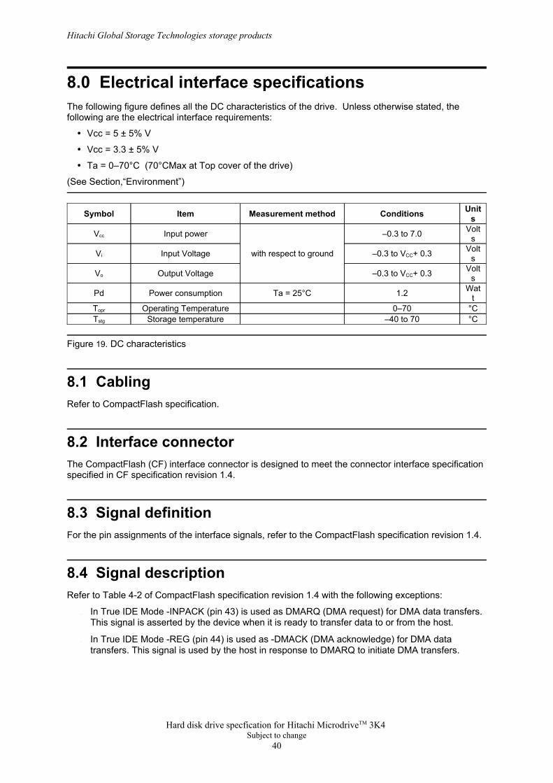
8.0 Electrical interface specificationsThe following figure defines all the DC characteristics of the drive. Unless otherwise stated, thefollowing are the electrical interface requirements:
Vcc = 5 ± 5% V
Vcc = 3.3 ± 5% V
Ta = 0–70°C (70°CMax at Top cover of the drive)
(See Section,“Environment”)
°C–40 to 70Storage temperatureTstg
°C0–70Operating TemperatureTopr
Watt1.2Ta = 25°CPower consumptionPd
Volts–0.3 to VCC+ 0.3Output VoltageVo
Volts–0.3 to VCC+ 0.3Input VoltageVi
Volts–0.3 to 7.0
with respect to ground
Input powerVcc
UnitsConditionsMeasurement methodItemSymbol
Figure 19. DC characteristics
8.1 CablingRefer to CompactFlash specification.
8.2 Interface connectorThe CompactFlash (CF) interface connector is designed to meet the connector interface specificationspecified in CF specification revision 1.4.
8.3 Signal definitionFor the pin assignments of the interface signals, refer to the CompactFlash specification revision 1.4.
8.4 Signal descriptionRefer to Table 4-2 of CompactFlash specification revision 1.4 with the following exceptions:
In True IDE Mode -INPACK (pin 43) is used as DMARQ (DMA request) for DMA data transfers.This signal is asserted by the device when it is ready to transfer data to or from the host.
In True IDE Mode -REG (pin 44) is used as -DMACK (DMA acknowledge) for DMA datatransfers. This signal is used by the host in response to DMARQ to initiate DMA transfers.
Hitachi Global Storage Technologies storage products
Hard disk drive specfication for Hitachi MicrodriveTM 3K4 Subject to change
40
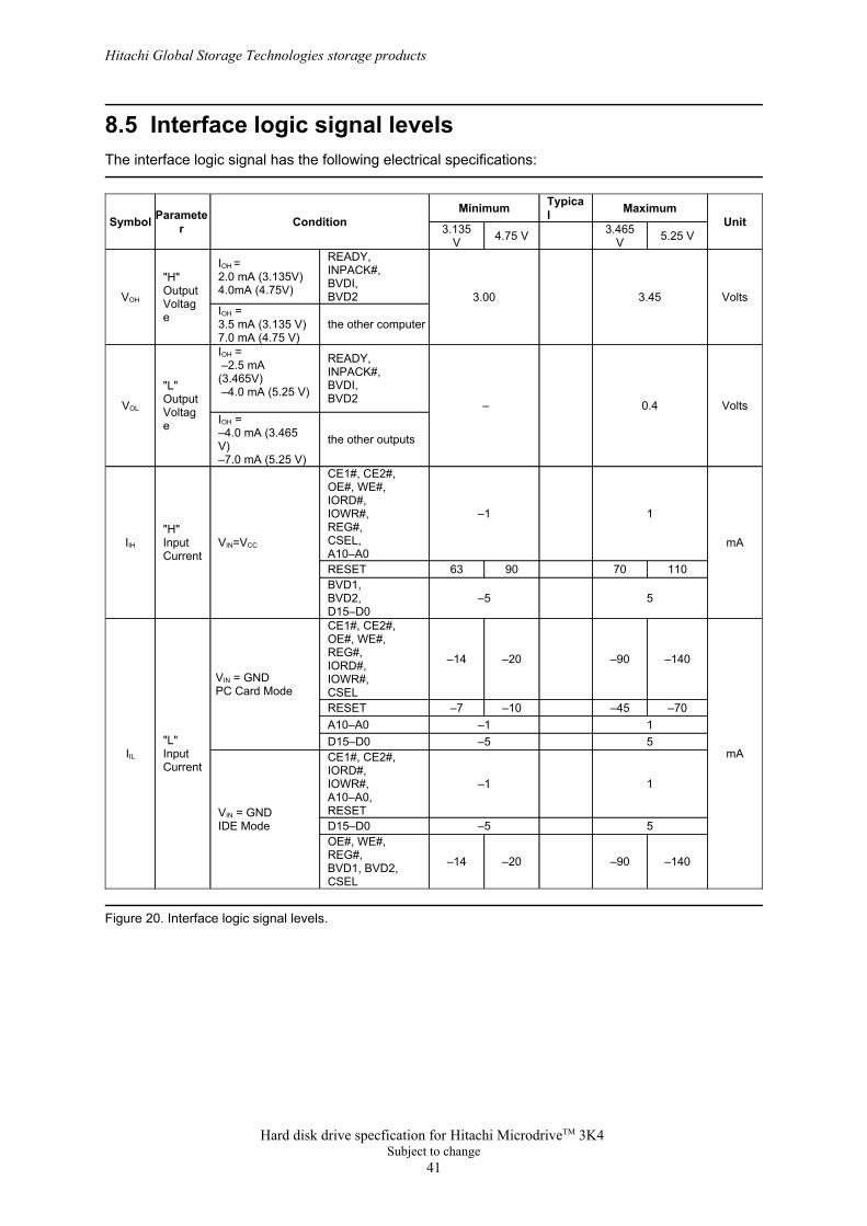
8.5 Interface logic signal levelsThe interface logic signal has the following electrical specifications:
–140–90–20–14
OE#, WE#,REG#,BVD1, BVD2,CSEL
5–5D15–D0
1–1
CE1#, CE2#,IORD#,IOWR#,A10–A0,RESETVIN = GND
IDE Mode
5–5D15–D01–1A10–A0
–70–45–10–7RESET
mA
–140–90–20–14
CE1#, CE2#,OE#, WE#,REG#,IORD#,IOWR#,CSEL
VIN = GNDPC Card Mode
"L"InputCurrent
IIL
5–5BVD1,BVD2,D15–D0
110709063RESET
mA
1–1
CE1#, CE2#,OE#, WE#,IORD#,IOWR#,REG#,CSEL,A10–A0
VIN=VCC
"H"InputCurrent
IIH
the other outputs
IOH = –4.0 mA (3.465V)–7.0 mA (5.25 V)
Volts0.4 –
READY,INPACK#,BVDI,BVD2
IOH = –2.5 mA(3.465V) –4.0 mA (5.25 V)"L"
OutputVoltage
VOL
the other computerIOH = 3.5 mA (3.135 V)7.0 mA (4.75 V)
Volts3.453.00
READY,INPACK#,BVDI,BVD2
IOH =2.0 mA (3.135V)4.0mA (4.75V)
"H"OutputVoltage
VOH
5.25 V3.465V4.75 V3.135
V
UnitMaximumTypica
l MinimumConditionParamete
rSymbol
Figure 20. Interface logic signal levels.
Hitachi Global Storage Technologies storage products
Hard disk drive specfication for Hitachi MicrodriveTM 3K4 Subject to change
41
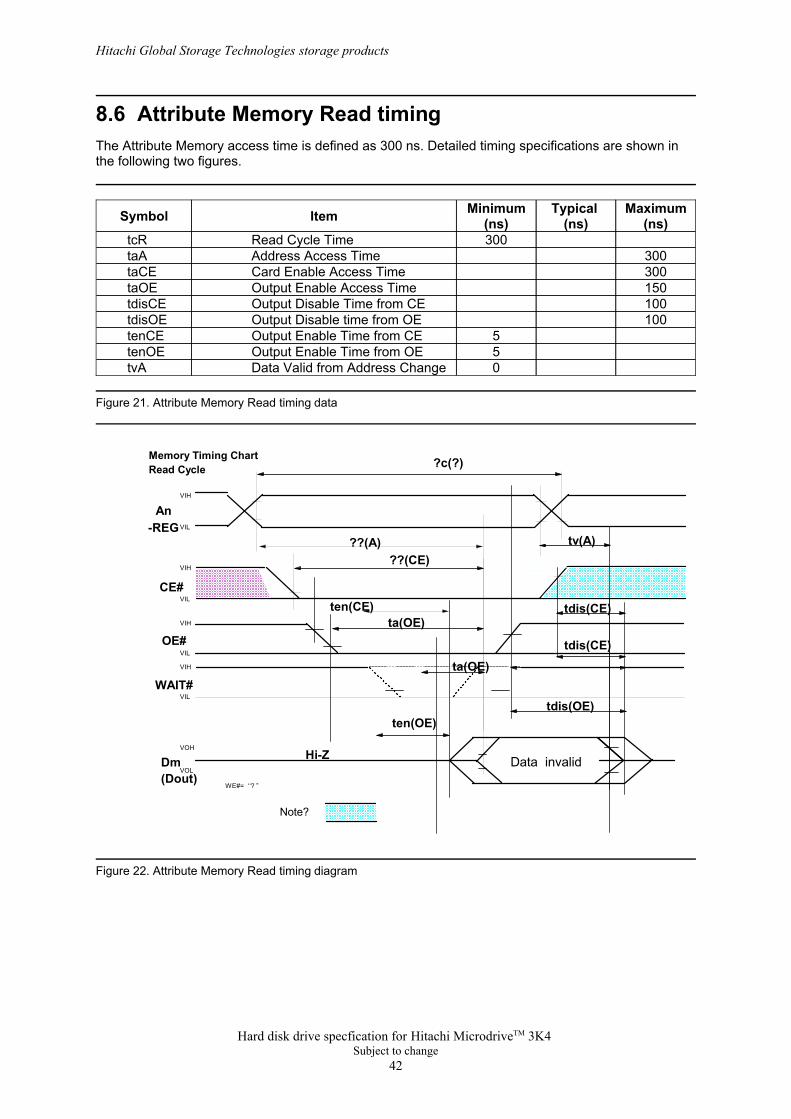
8.6 Attribute Memory Read timingThe Attribute Memory access time is defined as 300 ns. Detailed timing specifications are shown inthe following two figures.
0Data Valid from Address ChangetvA5Output Enable Time from OEtenOE5Output Enable Time from CEtenCE
100Output Disable time from OEtdisOE100Output Disable Time from CEtdisCE150Output Enable Access TimetaOE300Card Enable Access TimetaCE300Address Access TimetaA
300Read Cycle TimetcR
Maximum(ns)
Typical (ns)
Minimum(ns)ItemSymbol
Figure 21. Attribute Memory Read timing data
Data invalid
Memory Timing ChartRead Cycle
VIH
VIL
VIH
VIL
VIH
VIL
VOH
VOL
CE#
OE#
Dm(Dout)
WE#= ‘‘? ”
?c(?)
??(A)??(CE)
tv(A)
tdis(CE)ten(CE)ta(OE)
tdis(CE)
ten(OE)
Hi-Z
Note?
An-REG
VIH
VILWAIT#
ta(OE)
tdis(OE)
Figure 22. Attribute Memory Read timing diagram
Hitachi Global Storage Technologies storage products
Hard disk drive specfication for Hitachi MicrodriveTM 3K4 Subject to change
42
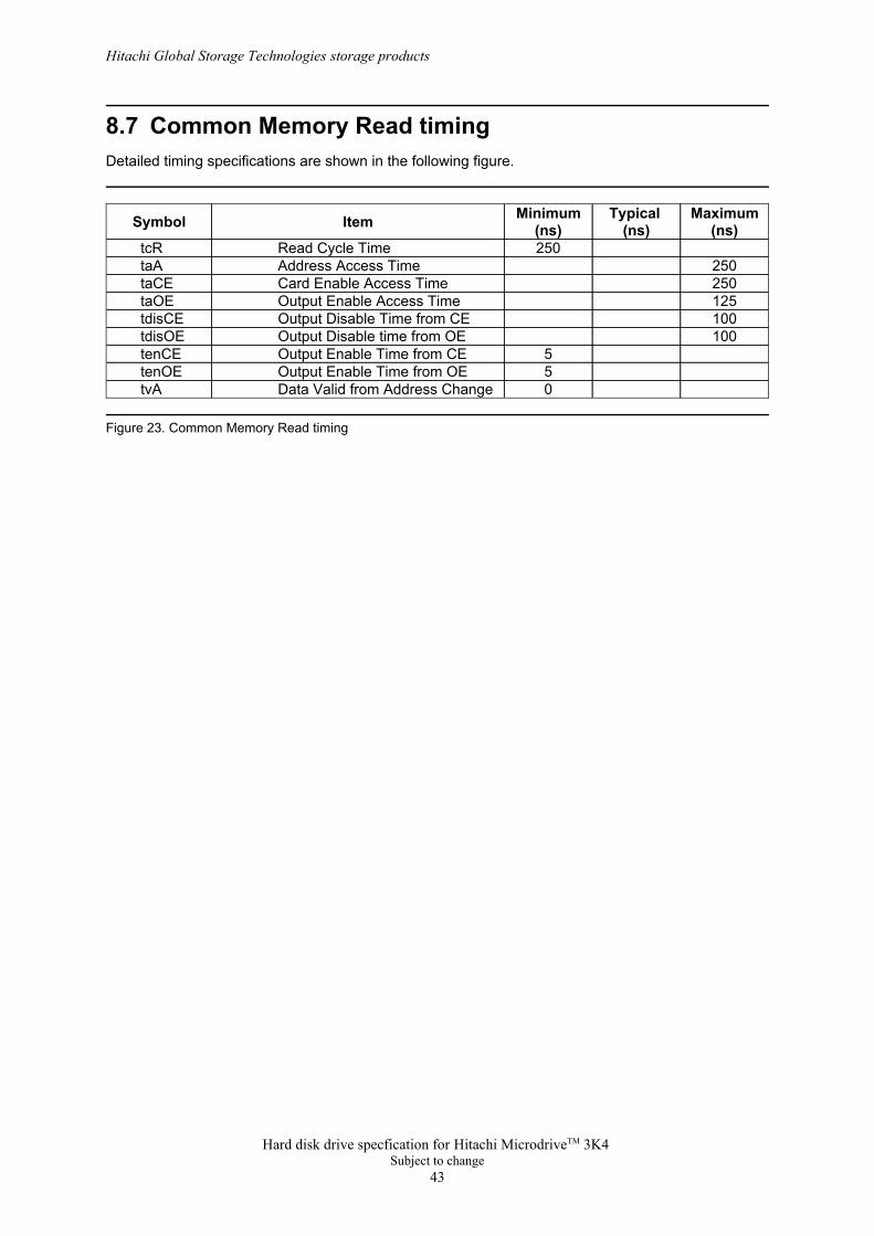
8.7 Common Memory Read timingDetailed timing specifications are shown in the following figure.
0Data Valid from Address ChangetvA5Output Enable Time from OEtenOE5Output Enable Time from CEtenCE
100Output Disable time from OEtdisOE100Output Disable Time from CEtdisCE125Output Enable Access TimetaOE250Card Enable Access TimetaCE250Address Access TimetaA
250Read Cycle TimetcR
Maximum(ns)
Typical (ns)
Minimum(ns)ItemSymbol
Figure 23. Common Memory Read timing
Hitachi Global Storage Technologies storage products
Hard disk drive specfication for Hitachi MicrodriveTM 3K4 Subject to change
43
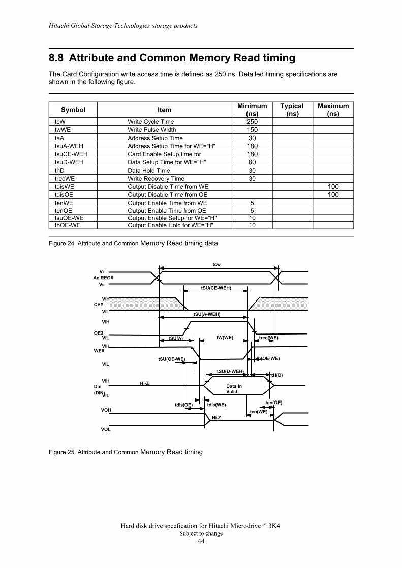
8.8 Attribute and Common Memory Read timingThe Card Configuration write access time is defined as 250 ns. Detailed timing specifications areshown in the following figure.
10Output Enable Hold for WE="H"thOE-WE10Output Enable Setup for WE="H"tsuOE-WE5Output Enable Time from OEtenOE5Output Enable Time from WEtenWE
100Output Disable Time from OEtdisOE100Output Disable Time from WEtdisWE
30Write Recovery TimetrecWE30Data Hold TimethD80Data Setup Time for WE="H"tsuD-WEH180Card Enable Setup time fortsuCE-WEH180Address Setup Time for WE="H"tsuA-WEH30Address Setup TimetaA150Write Pulse WidthtwWE250Write Cycle TimetcW
Maximum(ns)
Typical (ns)
Minimum(ns)ItemSymbol
Figure 24. Attribute and Common Memory Read timing data
Data In Valid
VIH
VIL
VIH
VIL
VIH
VIL
VIH
VIL
VIH
VIL
VOH
VOL
An,REG#
CE#
OE3
WE#
Dm(DIN)
tcw
tSU(CE-WEH)
tSU(A-WEH)
tSU(A) tW(WE)
tSU(OE-WE)
tSU(D-WEH)
trec(WE)
th(OE-WE)
tH(D)
Hi-Z
tdis(OE) tdis(WE)
Hi-Zten(WE)
ten(OE)
Figure 25. Attribute and Common Memory Read timing
Hitachi Global Storage Technologies storage products
Hard disk drive specfication for Hitachi MicrodriveTM 3K4 Subject to change
44
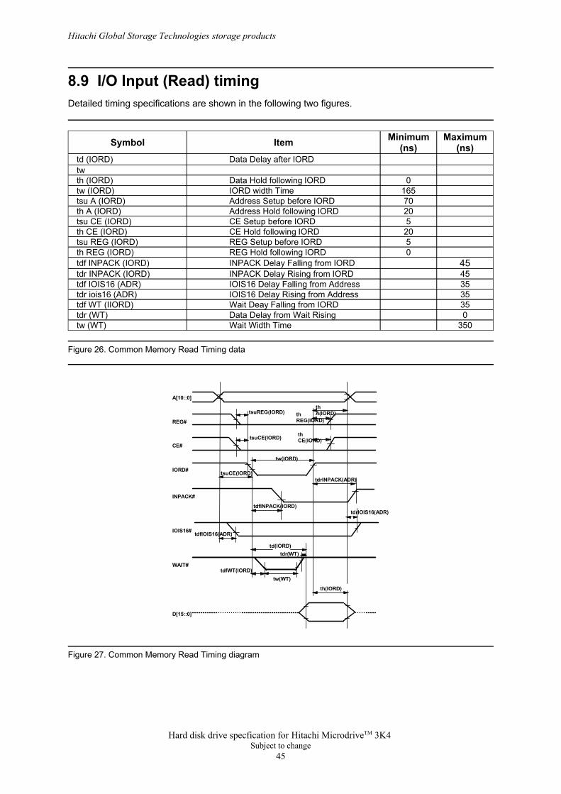
8.9 I/O Input (Read) timingDetailed timing specifications are shown in the following two figures.
350Wait Width Timetw (WT)0Data Delay from Wait Risingtdr (WT)
35Wait Deay Falling from IORDtdf WT (IIORD)35IOIS16 Delay Rising from Addresstdr iois16 (ADR)35IOIS16 Delay Falling from Addresstdf IOIS16 (ADR)45INPACK Delay Rising from IORDtdr INPACK (IORD)45INPACK Delay Falling from IORDtdf INPACK (IORD)
0REG Hold following IORDth REG (IORD)5REG Setup before IORDtsu REG (IORD)20CE Hold following IORDth CE (IORD)5CE Setup before IORDtsu CE (IORD)20Address Hold following IORDth A (IORD)70Address Setup before IORDtsu A (IORD)
165IORD width Timetw (IORD)0Data Hold following IORDth (IORD)
twData Delay after IORDtd (IORD)
Maximum(ns)
Minimum(ns)ItemSymbol
Figure 26. Common Memory Read Timing data
A[10::0]
REG#
CE#
IORD#
INPACK#
IOIS16#
WAIT#
D[15::0]
tsuREG(IORD)
tsuCE(IORD)
tsuCE(IORD)
tdfIOIS16(ADR)
tdfINPACK(IORD)
td(IORD)tdr(WT)
tw(WT)tdfWT(IORD)
th(IORD)
tdrIOIS16(ADR)
tdrINPACK(ADR)
tw(IORD)
th CE(IORD)
th A(IORD)th
REG(IORD)
Figure 27. Common Memory Read Timing diagram
Hitachi Global Storage Technologies storage products
Hard disk drive specfication for Hitachi MicrodriveTM 3K4 Subject to change
45
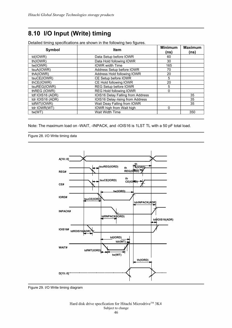
8.10 I/O Input (Write) timingDetailed timing specifications are shown in the following two figures.
350Wait Width Timetw(WT)0IOWR high from Wait hightdr IOWR(WT)
35Wait Deay Falling from IOWRtdfWT(IOWR)35IOIS16 Delay rising from Addresstdr IOIS16 (ADR)35IOIS16 Delay Falling from Addresstdf IOIS16 (ADR)
0REG Hold following IOWRthREG (IOWR)5REG Setup before IOWRtsuREG(IOWR)20CE Hold following IOWRthCE(IOWR)5CE Setup before IOWRtsuCE(IOWR)20Address Hold following IOWRthA(IOWR)70Address Setup before IOWRtsuA(IOWR)
165IOWR width Timetw(IOWR)30Data Hold following IOWRth(IOWR)60Data Setup before IOWRtd(IOWR)
Maximum(ns)
Minimum(ns)ItemSymbol
Note: The maximum load on -WAIT, -INPACK, and -IOIS16 is 1LST TL with a 50 pF total load.
Figure 28. I/O Write timing data
A[10::0]
REG#
CE#
IORD#
INPACK#
IOIS16#
WAIT#
D[15::0]
tsuREG(IORD)
tsuCE(IORD)
tsuCE(IORD)
tdfIOIS16(ADR)
tdfINPACK(IORD)
td(IORD)tdr(WT)
tw(WT)tdfWT(IORD)
th(IORD)
tdrIOIS16(ADR)
tdrINPACK(ADR)
tw(IORD)
th CE(IORD)
th A(IORD)th
REG(IORD)
Figure 29. I/O Write timing diagram
Hitachi Global Storage Technologies storage products
Hard disk drive specfication for Hitachi MicrodriveTM 3K4 Subject to change
46
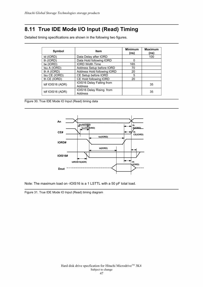
8.11 True IDE Mode I/O Input (Read) TimingDetailed timing specifications are shown in the following two figures.
35IOIS16 Delay Rising fromAddresstdf IOIS16 (ADR)
35IOIS16 Delay Falling fromAddresstdf IOIS16 (ADR)
20CE Hold following IORDth CE (IORD)5CE Setup before IORDtsu CE (IORD)
20Address Hold following IORDth A (IORD)70Address Setup before IORDtsu A (IORD)
165IORD Width Timetw (IORD)0Data Hold following IORDth (IORD)
100Data Delay after IORDtd (IORD)
Maximum(ns)
Minimum(ns)ItemSymbol
Figure 30. True IDE Mode IO Input (Read) timing data
An
Dout
CE#
IORD#
tsuCE(IORD)
tw(IORD)
th CE(IORD)
IOIS16#
tdfIOIS16(ADR)
tsuA(IORD)
td(IORD)
th A(IORD)
th (IORD)
Note: The maximum load on -IOIS16 is a 1 LSTTL with a 50 pF total load.
Figure 31. True IDE Mode IO Input (Read) timing diagram
Hitachi Global Storage Technologies storage products
Hard disk drive specfication for Hitachi MicrodriveTM 3K4 Subject to change
47
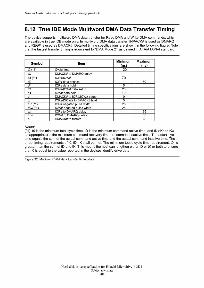
8.12 True IDE Mode Multiword DMA Data Transfer TimingThe device supports multiword DMA data transfer for Read DMA and Write DMA commands, whichare available in true IDE mode only. In multiword DMA data transfer, INPACK# is used as DMARQand REG# is used as DMACK#. Detailed timing specifications are shown in the following figure. Notethat the fastest transfer timing is equivalent to “DMA Mode 2” as defined in ATA/ATAPI-4 standard.
25DMACK# to tristatetZ35IOW# to DMARQ delaytLw35IOR# to DMARQ delaytLr
25IOW# negated pulse widthtKw (*1)25IOR# negated pulse widthtKr (*1)5IOR#/DIOW# to DMACK# holdtJ0DMACK# to IOR#/IOW# setuptI10IOW# data holdtH20IOR#/IOW# data setuptG5IOR# data holdtF
60IOR# data accesstE70IOR#/IOW#tD (*1)
DMACK# to DMARQ delaytC120Cycle timet0 (*1)
Maximum(ns)
Minimum(ns)ItemSymbol
Notes:(*1) t0 is the minimum total cycle time, tD is the minimum command active time, and tK (tKr or tKw,as appropriate) is the minimum command recovery time or command inactive time. The actual cycletime equals the sum of the actual command active time and the actual command inactive time. Thethree timing requirements of t0, tD, tK shall be met. The minimum tootle cycle time requirement, t0, isgreater than the sum of tD and tK. This means the host can lengthen either tD or tK or both to ensurethat t0 is equal to the value reported in the devices identify drive data.
Figure 32. Multiword DMA data transfer timing data
Hitachi Global Storage Technologies storage products
Hard disk drive specfication for Hitachi MicrodriveTM 3K4 Subject to change
48
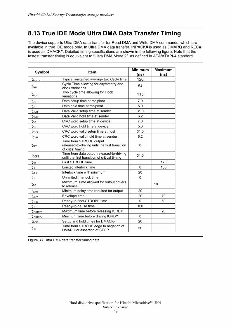
8.13 True IDE Mode Ultra DMA Data Transfer TimingThe device supports Ultra DMA data transfer for Read DMA and Write DMA commands, which areavailable in true IDE mode only. In Ultra DMA data transfer, INPACK# is used as DMARQ and REG#is used as DMACK#. Detailed timing specifications are shown in the following figure. Note that thefastest transfer timing is equivalent to “Ultra DMA Mode 2” as defined in ATA/ATAPI-4 standard.
50Time from STROBE edge to negation ofDMARQ or assertion of STOPtSS
20Setup and hold times for DMACK-tACK
0Minimum time before driving IORDYtIORDYY
20Maximum time before releasing IORDYtIORDYZ
100Ready-to-pause timetRP
600Ready-to-final-STROBE timetRFS
7020Envelope timetENV
20Minimum delay time required for outputtZAH
10Maximum Time allowed for output driversto releasetAZ
0Unlimited interlock timetUI
20Interlock time with minimumtMLI
150 0 Limited interlock timetLI
170First STROBE timetFS
31.0Time from data output released-to-drivinguntil the first transition of critical timingtDZFS
0Time from STROBE outputreleased-to-driving until the first transitionof critial timing
tZFS
6.2CRC word valid hold time at sendertCVH
31.0CRC word valid setup time at hosttCVS
5.0CRC word hold time at devicetCH
7.0CRC word setup time at devicetCS
6.2Data Valid hold time at sendertDVH
31.0Data Valid setup time at sendertDVS
5.0Data hold time at recipienttDH
7.0Data setup time at recipienttDS
115Two cycle time allowing for clockvariationst2cyc
54Cycle Time allowing for asymmetry andclock variationstcyc
120Typical sustained average two Cycle timet2cyctyp
Maximum(ns)
Minimum(ns)ItemSymbol
Figure 33. Ultra DMA data transfer timing data
Hitachi Global Storage Technologies storage products
Hard disk drive specfication for Hitachi MicrodriveTM 3K4 Subject to change
49
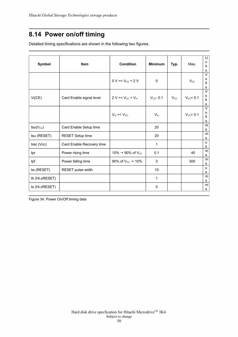
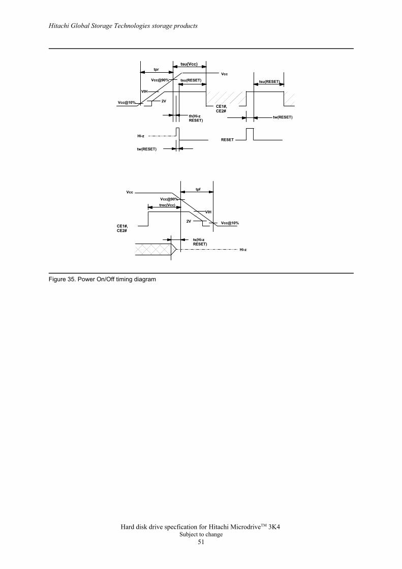
8.14 Power on/off timingDetailed timing specifications are shown in the following two figures.
ms0ts (Hi-zRESET)
ms1th (Hi-zRESET)
us10RESET pulse widthtw (RESET)
ms300390% of VCC 10%Power falling timetpf
ms 400.110% 90% of VCCPower rising timetpr
us1Card Enable Recovery timetrec (Vcc)
ms20RESET Setup timetsu (RESET)
ms20Card Enable Setup timetsu(VCC)
Volts
VCC+ 0.1VIHVIH =< VCC
Volts
VCC+ 0.1VCCVCC- 0.12 V =< VCC < VIH Card Enable signal levelVi(CE)
Volts
VCC00 V =< VCC < 2 V
Units
Max.Typ.MinimumConditionItemSymbol
Figure 34. Power On/Off timing data
Hitachi Global Storage Technologies storage products
Hard disk drive specfication for Hitachi MicrodriveTM 3K4 Subject to change
50
tprtsu(Vcc)
VccVcc@90%
Vcc@10%
VIH
2V
tsu(RESET)
th(Hi-z RESET)
tsu(RESET)
tw(RESET)
RESET
tw(RESET)
Hi-z
Vcc
Vcc@90%trec(Vcc)
VIH
Vcc@10%2V
ts(Hi-z RESET)
Hi-z
tpf
CE1#, CE2#
CE1#, CE2#
Figure 35. Power On/Off timing diagram
Hitachi Global Storage Technologies storage products
Hard disk drive specfication for Hitachi MicrodriveTM 3K4 Subject to change
51
Part 2. Interface specification
Hitachi Global Storage Technologies storage products
Hard disk drive specfication for Hitachi MicrodriveTM 3K4 Subject to change
52
9 General
9.1 IntroductionThis part of specification describes the host interface of Hitachi Microdrive 3K4.The interface conforms to the CF+ and CompactFlash Specification with certainlimitations described in " 2 Deviations from Standard " on page 0.Hitachi Microdrive<ProductName> 3K4 following new functions included byCompactFlash Specification 1.4 or newer standard.
Hitachi Microdrive 3K4 support following functions as Vendor Specific Function.SENSE CONDITION commandFormat Unit commandMetadata Storage Function
The following terminology is used in this part of specification.
Interrupt request (Device or Host) INTRQ
The command which is executed first right after power on reset or hard resetwhen the initial power mode at power on is Standby mode.
First Command
Host indicates the system that the device is attached to. Host
Device indicates Hitachi Microdrive 3K4 Device
Hitachi Global Storage Technologies storage products
Hard disk drive specfication for Hitachi MicrodriveTM 3K4 Subject to change
53
10 Deviations from Standard
WRITE VERIFY command does not include read verification after writeoperation. The function is exactly same as WRITE SECTORS command.
Write Verify
If STANDBY command or IDLE command is used with the Sector CountRegister being zero, the standby timer is programmed to 109 minutes,instead of disabling automatic standby function. Note that if the advancedpower management level is less than 80h, which is power-on default, thetransition timing to enter Standby mode is determined by either thestandby timer or Adaptive Battery File Extender algorithm, whichevermeets the condition first.
Standby Timer
The device supports Ultra DMA transfer mode. BBK bit in Error registeris replaced by ICRCE ( Interface CRC Error ) bit.
ICRCE (CRC)
Hitachi Global Storage Technologies storage products
Hard disk drive specfication for Hitachi MicrodriveTM 3K4 Subject to change
54
11 System interface
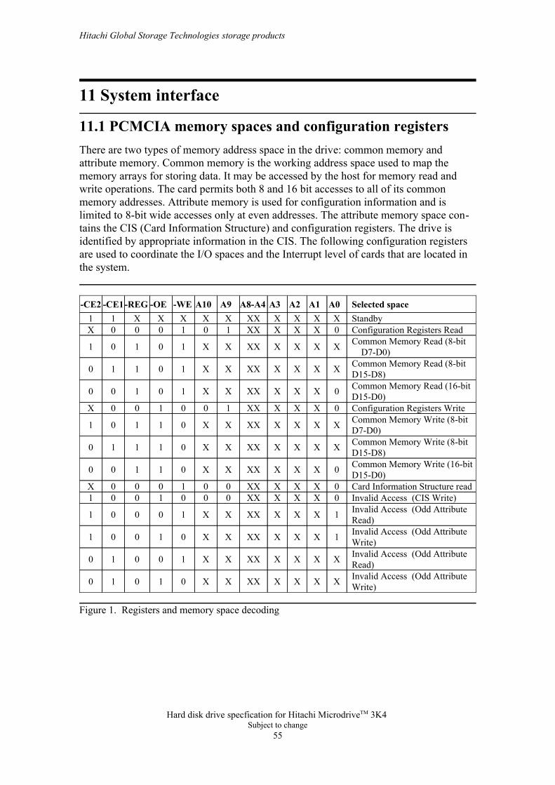
11.1 PCMCIA memory spaces and configuration registers There are two types of memory address space in the drive: common memory andattribute memory. Common memory is the working address space used to map thememory arrays for storing data. It may be accessed by the host for memory read andwrite operations. The card permits both 8 and 16 bit accesses to all of its commonmemory addresses. Attribute memory is used for configuration information and islimited to 8-bit wide accesses only at even addresses. The attribute memory space con-tains the CIS (Card Information Structure) and configuration registers. The drive isidentified by appropriate information in the CIS. The following configuration registersare used to coordinate the I/O spaces and the Interrupt level of cards that are located inthe system.
Invalid Access (Odd AttributeWrite)XXXXXXXX01010
Invalid Access (Odd AttributeRead)XXXXXXXX10010
Invalid Access (Odd AttributeWrite)1XXXXXXX01001
Invalid Access (Odd AttributeRead)1XXXXXXX10001
Invalid Access (CIS Write)0XXXXX0001001Card Information Structure read0XXXXX001000X
Common Memory Write (16-bitD15-D0)0XXXXXXX01100
Common Memory Write (8-bitD15-D8)XXXXXXXX01110
Common Memory Write (8-bitD7-D0)XXXXXXXX01101
Configuration Registers Write0XXXXX100100X
Common Memory Read (16-bitD15-D0)0XXXXXXX10100
Common Memory Read (8-bitD15-D8)XXXXXXXX10110
Common Memory Read (8-bit D7-D0)XXXXXXXX10101
Configuration Registers Read0XXXXX101000XStandbyXXXXXXXXXXX11Selected spaceA0A1A2A3A8-A4A9A10-WE-OE-REG-CE1-CE2
Figure 1. Registers and memory space decoding
Hitachi Global Storage Technologies storage products
Hard disk drive specfication for Hitachi MicrodriveTM 3K4 Subject to change
55
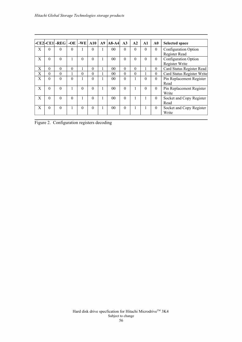
Socket and Copy RegisterWrite
011000100100X
Socket and Copy RegisterRead
011000101000X
Pin Replacement RegisterWrite
001000100100X
Pin Replacement RegisterRead
001000101000XCard Status Register Write010000100100XCard Status Register Read010000101000X
Configuration OptionRegister Write
000000100100X
Configuration OptionRegister Read
000000101000XSelected spaceA0A1A2A3A8-A4A9A10-WE-OE-REG-CE1-CE2
Figure 2. Configuration registers decoding
Hitachi Global Storage Technologies storage products
Hard disk drive specfication for Hitachi MicrodriveTM 3K4 Subject to change
56
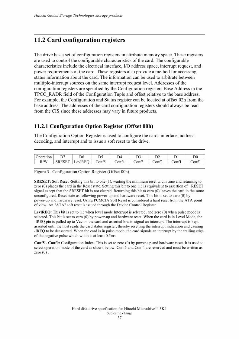
11.2 Card configuration registers
The drive has a set of configuration registers in attribute memory space. These registersare used to control the configurable characteristics of the card. The configurablecharacteristics include the electrical interface, I/O address space, interrupt request, andpower requirements of the card. These registers also provide a method for accessingstatus information about the card. The information can be used to arbitrate betweenmultiple-interrupt sources on the same interrupt request level. Addresses of theconfiguration registers are specified by the Configuration registers Base Address in theTPCC_RADR field of the Configuration Tuple and offset relative to the base address.For example, the Configuration and Status register can be located at offset 02h from thebase address. The addresses of the card configuration registers should always be readfrom the CIS since these addresses may vary in future products.
11.2.1 Configuration Option Register (Offset 00h)The Configuration Option Register is used to configure the cards interface, addressdecoding, and interrupt and to issue a soft reset to the drive.
Conf0Conf1Conf2Conf3Conf4Conf5LevlREQSRESETR/WD0D1D2D3D4D5D6D7Operation
Figure 3. Configuration Option Register (Offset 00h)
SRESET: Soft Reset -Setting this bit to one (1), waiting the minimum reset width time and returning tozero (0) places the card in the Reset state. Setting this bit to one (1) is equivalent to assertion of +RESETsignal except that the SRESET bit is not cleared. Returning this bit to zero (0) leaves the card in the sameunconfigured, Reset state as following power-up and hardware reset. This bit is set to zero (0) bypower-up and hardware reset. Using PCMCIA Soft Reset is considered a hard reset from the ATA pointof view. An "ATA" soft reset is issued through the Device Control Register.
LevlREQ: This bit is set to (1) when level mode Interrupt is selected, and zero (0) when pulse mode isselected. This bit is set to zero (0) by power-up and hardware reset. When the card is in Level Mode, the-IREQ pin is pulled up to Vcc on the card and asserted low to signal an interrupt. The interrupt is keptasserted until the host reads the card status register, thereby resetting the interrupt indication and causing-IREQ to be deasserted. When the card is in pulse mode, the card signals an interrupt by the trailing edgeof the negative pulse which width is at least 0.5ms.
Conf5 - Conf0: Configuration Index. This is set to zero (0) by power-up and hardware reset. It is used toselect operation mode of the card as shown below. Conf5 and Conf4 are reserved and must be written aszero (0) .
Hitachi Global Storage Technologies storage products
Hard disk drive specfication for Hitachi MicrodriveTM 3K4 Subject to change
57
Secondary I/O mapped, 170h n 177h/376h n377h110000
Primary I/O mapped, 1F0h n 1F7h/3F6h n3F7h010000
I/O mapped 16 contiguous registers at any16-byte system decoded boundary100000
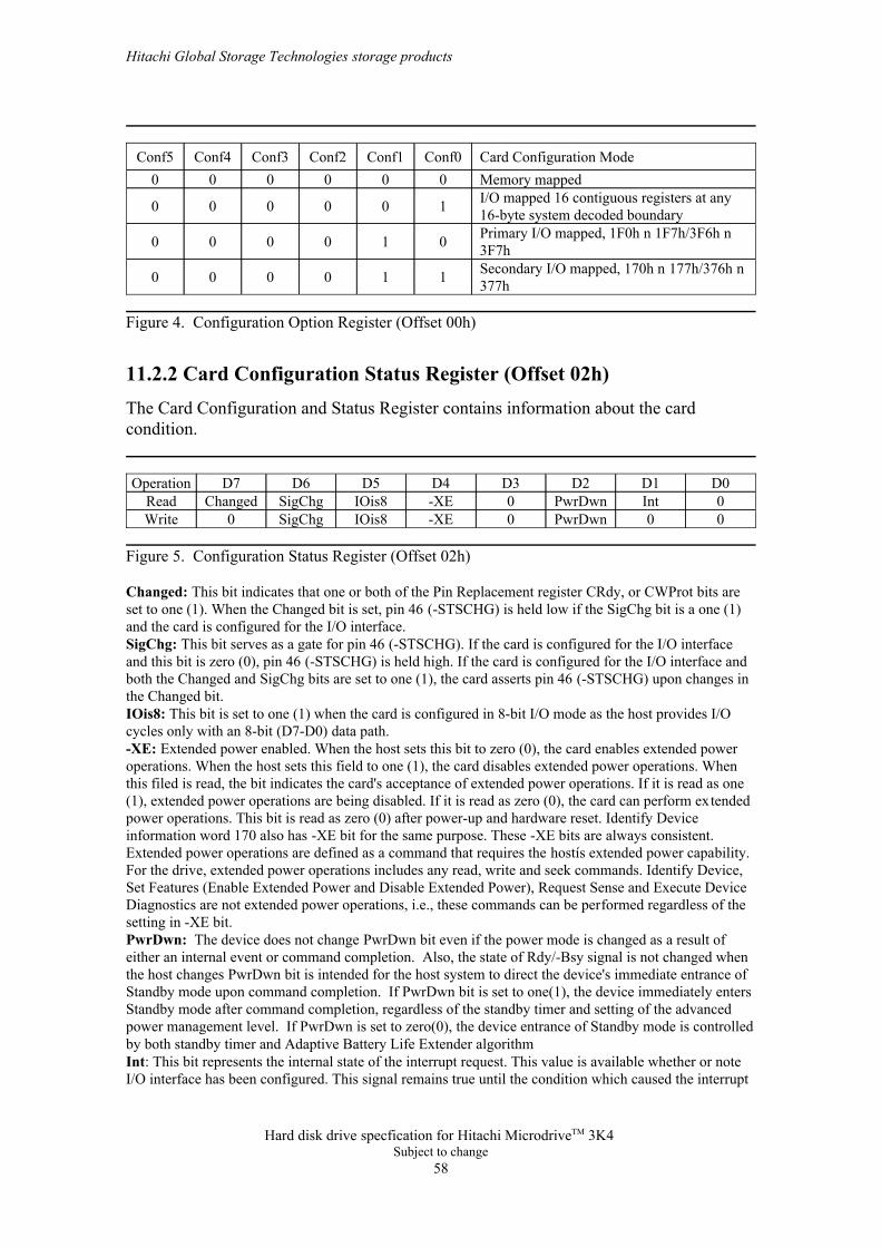
Memory mapped000000Card Configuration ModeConf0Conf1Conf2Conf3Conf4Conf5
Figure 4. Configuration Option Register (Offset 00h)
11.2.2 Card Configuration Status Register (Offset 02h)The Card Configuration and Status Register contains information about the cardcondition.
00PwrDwn0-XEIOis8SigChg0Write0IntPwrDwn0-XEIOis8SigChgChangedRead
D0D1D2D3D4D5D6D7Operation
Figure 5. Configuration Status Register (Offset 02h)
Changed: This bit indicates that one or both of the Pin Replacement register CRdy, or CWProt bits areset to one (1). When the Changed bit is set, pin 46 (-STSCHG) is held low if the SigChg bit is a one (1)and the card is configured for the I/O interface.SigChg: This bit serves as a gate for pin 46 (-STSCHG). If the card is configured for the I/O interfaceand this bit is zero (0), pin 46 (-STSCHG) is held high. If the card is configured for the I/O interface andboth the Changed and SigChg bits are set to one (1), the card asserts pin 46 (-STSCHG) upon changes inthe Changed bit.IOis8: This bit is set to one (1) when the card is configured in 8-bit I/O mode as the host provides I/Ocycles only with an 8-bit (D7-D0) data path.-XE: Extended power enabled. When the host sets this bit to zero (0), the card enables extended poweroperations. When the host sets this field to one (1), the card disables extended power operations. Whenthis filed is read, the bit indicates the card's acceptance of extended power operations. If it is read as one(1), extended power operations are being disabled. If it is read as zero (0), the card can perform extendedpower operations. This bit is read as zero (0) after power-up and hardware reset. Identify Deviceinformation word 170 also has -XE bit for the same purpose. These -XE bits are always consistent.Extended power operations are defined as a command that requires the hostís extended power capability.For the drive, extended power operations includes any read, write and seek commands. Identify Device,Set Features (Enable Extended Power and Disable Extended Power), Request Sense and Execute DeviceDiagnostics are not extended power operations, i.e., these commands can be performed regardless of thesetting in -XE bit.PwrDwn: The device does not change PwrDwn bit even if the power mode is changed as a result ofeither an internal event or command completion. Also, the state of Rdy/-Bsy signal is not changed whenthe host changes PwrDwn bit is intended for the host system to direct the device's immediate entrance ofStandby mode upon command completion. If PwrDwn bit is set to one(1), the device immediately entersStandby mode after command completion, regardless of the standby timer and setting of the advancedpower management level. If PwrDwn is set to zero(0), the device entrance of Standby mode is controlledby both standby timer and Adaptive Battery Life Extender algorithm Int: This bit represents the internal state of the interrupt request. This value is available whether or noteI/O interface has been configured. This signal remains true until the condition which caused the interrupt
Hitachi Global Storage Technologies storage products
Hard disk drive specfication for Hitachi MicrodriveTM 3K4 Subject to change
58
request has been serviced. If interrupts are disabled byte -IEN bit in the Device Control Register, this bitis zero (0).
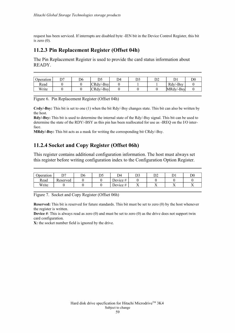
11.2.3 Pin Replacement Register (Offset 04h)
The Pin Replacement Register is used to provide the card status information aboutREADY.
0MRdy/-Bsy000CRdy/-Bsy00Write0Rdy/-Bsy110CRdy/-Bsy00Read
D0D1D2D3D4D5D6D7Operation
Figure 6. Pin Replacement Register (Offset 04h)
Crdy/-Bsy: This bit is set to one (1) when the bit Rdy/-Bsy changes state. This bit can also be written bythe host.Rdy/-Bsy: This bit is used to determine the internal state of the Rdy/-Bsy signal. This bit can be used todetermine the state of the RDY/-BSY as this pin has been reallocated for use as -IREQ on the I/O inter-face.MRdy/-Bsy: This bit acts as a mask for writing the corresponding bit CRdy/-Bsy.
11.2.4 Socket and Copy Register (Offset 06h)This register contains additional configuration information. The host must always setthis register before writing configuration index to the Configuration Option Register.
XXXXDevice #000Write0000Device #00ReservedRead
D0D1D2D3D4D5D6D7Operation
Figure 7. Socket and Copy Register (Offset 06h)
Reserved: This bit is reserved for future standards. This bit must be set to zero (0) by the host wheneverthe register is written.Device #: This is always read as zero (0) and must be set to zero (0) as the drive does not support twincard configuration.X: the socket number field is ignored by the drive.
Hitachi Global Storage Technologies storage products
Hard disk drive specfication for Hitachi MicrodriveTM 3K4 Subject to change
59
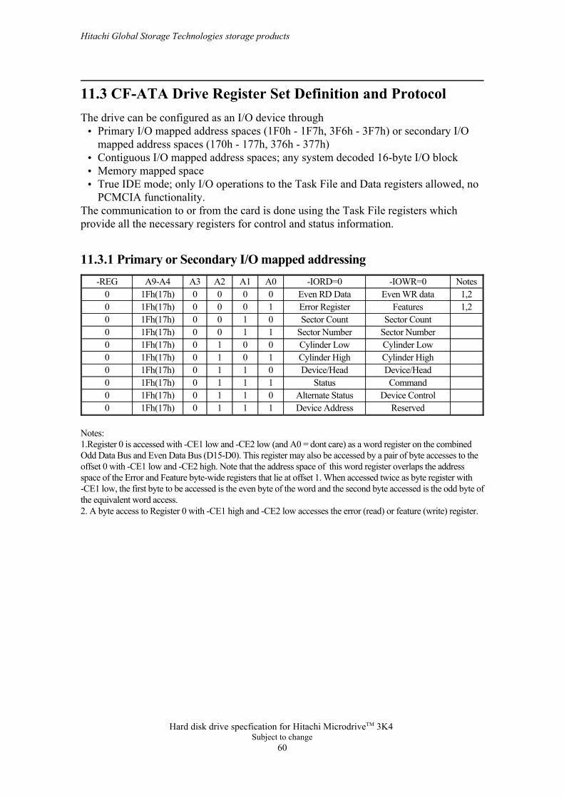
11.3 CF-ATA Drive Register Set Definition and ProtocolThe drive can be configured as an I/O device through
Primary I/O mapped address spaces (1F0h - 1F7h, 3F6h - 3F7h) or secondary I/Omapped address spaces (170h - 177h, 376h - 377h)Contiguous I/O mapped address spaces; any system decoded 16-byte I/O blockMemory mapped spaceTrue IDE mode; only I/O operations to the Task File and Data registers allowed, noPCMCIA functionality.
The communication to or from the card is done using the Task File registers whichprovide all the necessary registers for control and status information.
11.3.1 Primary or Secondary I/O mapped addressing
ReservedDevice Address11101Fh(17h)0Device ControlAlternate Status01101Fh(17h)0
CommandStatus11101Fh(17h)0Device/HeadDevice/Head01101Fh(17h)0Cylinder HighCylinder High10101Fh(17h)0Cylinder LowCylinder Low00101Fh(17h)0Sector NumberSector Number11001Fh(17h)0Sector CountSector Count01001Fh(17h)0
1,2FeaturesError Register10001Fh(17h)01,2Even WR dataEven RD Data00001Fh(17h)0
Notes-IOWR=0-IORD=0A0A1A2A3A9-A4-REG
Notes:1.Register 0 is accessed with -CE1 low and -CE2 low (and A0 = dont care) as a word register on the combinedOdd Data Bus and Even Data Bus (D15-D0). This register may also be accessed by a pair of byte accesses to theoffset 0 with -CE1 low and -CE2 high. Note that the address space of this word register overlaps the addressspace of the Error and Feature byte-wide registers that lie at offset 1. When accessed twice as byte register with-CE1 low, the first byte to be accessed is the even byte of the word and the second byte accessed is the odd byte ofthe equivalent word access.2. A byte access to Register 0 with -CE1 high and -CE2 low accesses the error (read) or feature (write) register.
Hitachi Global Storage Technologies storage products
Hard disk drive specfication for Hitachi MicrodriveTM 3K4 Subject to change
60
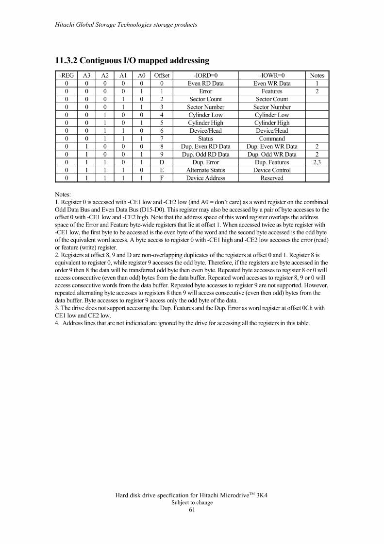
11.3.2 Contiguous I/O mapped addressing
ReservedDevice AddressF11110Device ControlAlternate StatusE01110
2,3Dup. FeaturesDup. ErrorD101102Dup. Odd WR DataDup. Odd RD Data9100102Dup. Even WR DataDup. Even RD Data800010
CommandStatus711100Device/HeadDevice/Head601100Cylinder HighCylinder High510100Cylinder LowCylinder Low400100Sector NumberSector Number311000Sector CountSector Count201000
2FeaturesError1100001Even WR DataEven RD Data000000
Notes-IOWR=0-IORD=0OffsetA0A1A2A3-REG
Notes:1. Register 0 is accessed with -CE1 low and -CE2 low (and A0 = don’t care) as a word register on the combinedOdd Data Bus and Even Data Bus (D15-D0). This register may also be accessed by a pair of byte accesses to theoffset 0 with -CE1 low and -CE2 high. Note that the address space of this word register overlaps the addressspace of the Error and Feature byte-wide registers that lie at offset 1. When accessed twice as byte register with-CE1 low, the first byte to be accessed is the even byte of the word and the second byte accessed is the odd byteof the equivalent word access. A byte access to register 0 with -CE1 high and -CE2 low accesses the error (read)or feature (write) register.2. Registers at offset 8, 9 and D are non-overlapping duplicates of the registers at offset 0 and 1. Register 8 isequivalent to register 0, while register 9 accesses the odd byte. Therefore, if the registers are byte accessed in theorder 9 then 8 the data will be transferred odd byte then even byte. Repeated byte accesses to register 8 or 0 willaccess consecutive (even than odd) bytes from the data buffer. Repeated word accesses to register 8, 9 or 0 willaccess consecutive words from the data buffer. Repeated byte accesses to register 9 are not supported. However,repeated alternating byte accesses to registers 8 then 9 will access consecutive (even then odd) bytes from thedata buffer. Byte accesses to register 9 access only the odd byte of the data.3. The drive does not support accessing the Dup. Features and the Dup. Error as word register at offset 0Ch withCE1 low and CE2 low.4. Address lines that are not indicated are ignored by the drive for accessing all the registers in this table.
Hitachi Global Storage Technologies storage products
Hard disk drive specfication for Hitachi MicrodriveTM 3K4 Subject to change
61
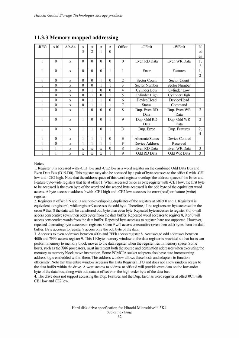
11.3.3 Memory mapped addressing
3Odd WR DataOdd RD Data91xxxx113Even WR DataEven RD Data80xxxx11
ReservedDevice AddressF1111x01Device ControlAlternate StatusE0111x01
2,4
Dup. FeaturesDup. ErrorD1011x01
2Dup. Odd WRData
Dup. Odd RDData
91001x01
2Dup. Even WRData
Dup. Even RDData
80001x01CommandStatus71110x01
Device/HeadDevice/Head60110x01Cylinder HighCylinder High51010x01Cylinder LowCylinder Low40010x01Sector NumberSector Number31100x01Sector CountSector Count20100x01
1,2
FeaturesError11000x01
1,2
Even WR DataEven RD Data00000x01
Notes
-WE=0-OE=0OffsetA0
A1
A2
A3
A9-A4A10-REG
Notes:1. Register 0 is accessed with -CE1 low and -CE2 low as a word register on the combined Odd Data Bus andEven Data Bus (D15-D0). This register may also be accessed by a pair of byte accesses to the offset 0 with -CE1low and -CE2 high. Note that the address space of this word register overlaps the address space of the Error andFeature byte-wide registers that lie at offset 1. When accessed twice as byte register with -CE1 low, the first byteto be accessed is the even byte of the word and the second byte accessed is the odd byte of the equivalent wordaccess. A byte access to address 0 with -CE1 high and -CE2 low accesses the error (read) or feature (write)register.2. Registers at offset 8, 9 and D are non-overlapping duplicates of the registers at offset 0 and 1. Register 8 isequivalent to register 0, while register 9 accesses the odd byte. Therefore, if the registers are byte accessed in theorder 9 then 8 the data will be transferred odd byte then even byte. Repeated byte accesses to register 8 or 0 willaccess consecutive (even then odd) bytes from the data buffer. Repeated word accesses to register 8, 9 or 0 willaccess consecutive words from the data buffer. Repeated byte accesses to register 9 are not supported. However,repeated alternating byte accesses to registers 8 then 9 will access consecutive (even then odd) bytes from the databuffer. Byte accesses to register 9 access only the odd byte of the data.3. Accesses to even addresses between 400h and 7FFh access register 8. Accesses to odd addresses between400h and 7FFh access register 9. This 1 Kbyte memory window to the data register is provided so that hosts canperform memory to memory block moves to the data register when the register lies in memory space. Somehosts, such as the X86 processors, must increment both the source and destination addresses when executing thememory to memory block move instruction. Some PCMCIA socket adapters also have auto incrementingaddress logic embedded within them. This address window allows these hosts and adapters to functionefficiently. Note that this entire window accesses the Data Register FIFO and does not allow random access tothe data buffer within the drive. A word access to address at offset 8 will provide even data on the low-orderbyte of the data bus, along with odd data at offset 9 on the high-order byte of the data bus. 4. The drive does not support accessing the Dup. Features and the Dup. Error as word register at offset 0Ch withCE1 low and CE2 low.
Hitachi Global Storage Technologies storage products
Hard disk drive specfication for Hitachi MicrodriveTM 3K4 Subject to change
62
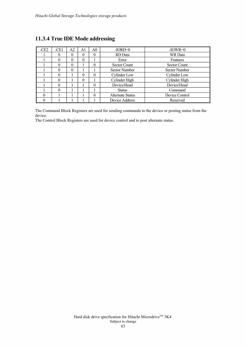
11.3.4 True IDE Mode addressing
ReservedDevice Address11110Device ControlAlternate Status01110
CommandStatus11101Device/HeadDevice/Head01101Cylinder HighCylinder High10101Cylinder LowCylinder Low00101Sector NumberSector Number11001Sector CountSector Count01001
FeaturesError10001WR DataRD Data00001-IOWR=0-IORD=0A0A1A2-CE1-CE2
The Command Block Registers are used for sending commands to the device or posting status from thedevice.The Control Block Registers are used for device control and to post alternate status.
Hitachi Global Storage Technologies storage products
Hard disk drive specfication for Hitachi MicrodriveTM 3K4 Subject to change
63
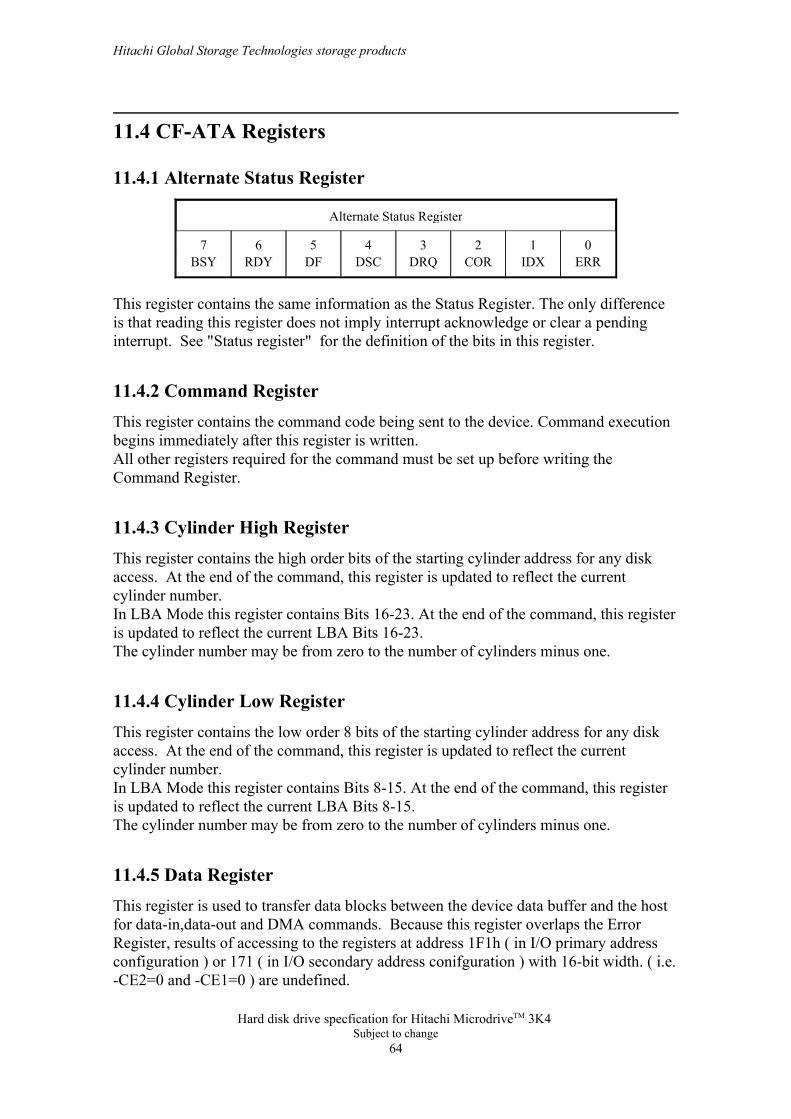
11.4 CF-ATA Registers
11.4.1 Alternate Status Register
ERRIDXCORDRQDSCDFRDYBSY01234567
Alternate Status Register
This register contains the same information as the Status Register. The only differenceis that reading this register does not imply interrupt acknowledge or clear a pendinginterrupt. See "Status register" for the definition of the bits in this register.
11.4.2 Command Register This register contains the command code being sent to the device. Command executionbegins immediately after this register is written. All other registers required for the command must be set up before writing theCommand Register.
11.4.3 Cylinder High Register This register contains the high order bits of the starting cylinder address for any diskaccess. At the end of the command, this register is updated to reflect the currentcylinder number.In LBA Mode this register contains Bits 16-23. At the end of the command, this registeris updated to reflect the current LBA Bits 16-23.The cylinder number may be from zero to the number of cylinders minus one.
11.4.4 Cylinder Low Register This register contains the low order 8 bits of the starting cylinder address for any diskaccess. At the end of the command, this register is updated to reflect the currentcylinder number.In LBA Mode this register contains Bits 8-15. At the end of the command, this registeris updated to reflect the current LBA Bits 8-15.The cylinder number may be from zero to the number of cylinders minus one.
11.4.5 Data Register This register is used to transfer data blocks between the device data buffer and the hostfor data-in,data-out and DMA commands. Because this register overlaps the ErrorRegister, results of accessing to the registers at address 1F1h ( in I/O primary addressconfiguration ) or 171 ( in I/O secondary address conifguration ) with 16-bit width. ( i.e.-CE2=0 and -CE1=0 ) are undefined.
Hitachi Global Storage Technologies storage products
Hard disk drive specfication for Hitachi MicrodriveTM 3K4 Subject to change
64
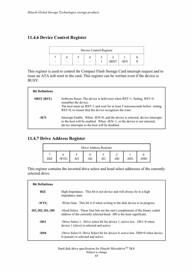
11.4.6 Device Control Register
0-IENSRST1----01234567
Device Control Register
This register is used to control thr Compact Flash Storage Card interrupt request and toissue an ATA soft reset to the card. This register can be wrriten even if the device isBUSY.
Interrupt Enable. When -IEN=0, and the device is selected, device interruptsto the host will be enabled. When -IEN=1, or the device is not selected,device interrupts to the host will be disabled.
-IEN
Software Reset. The device is held reset when RST=1. Setting RST=0reenables the device.The host must set RST=1 and wait for at least 5 microseconds before settingRST=0, to ensure that the device recognizes the reset.
SRST (RST)
Bit Definitions
11.4.7 Drive Address Register
-DS0-DS1-H0-H1-H2-H3-WTGHIZ01234567
Drive Address Register
This register contains the inverted drive select and head select addresses of the currentlyselected drive.
-Drive Select 0. Drive Select bit for device 0, active low. DS0=0 when device0 (master) is selected and active.
-DS0
-Drive Select 1. Drive select bit for device 1, active low. DS1=0 whendevice 1 (slave) is selected and active.
-DS1
-Head Select. These four bits are the one's complement of the binary codedaddress of the currently selected head. -H0 is the least significant.
-H3,-H2,-H1,-H0
-Write Gate. This bit is 0 when writing to the disk device is in progress.-WTG
High Impedance. This bit is not device and will always be in a highimpedance state.
HIZ
Bit Definitions
Hitachi Global Storage Technologies storage products
Hard disk drive specfication for Hitachi MicrodriveTM 3K4 Subject to change
65
11.4.8 Device/Head Register
HS0HS1HS2HS3DRV1L101234567
Device/Head Register
This register contains the device and head numbers.
Head Select. These four bits indicate binary encoded address of the head.HS0 is the least significant bit. At command completion, these bits areupdated to reflect the currently selected head.The head number may be from zero to the number of heads minus one.In LBA mode, HS3 through HS0 contain bits 24-27 of the LBA. Atcommand completion, these bits are updated to reflect the current LBA bits24-27.
HS3,HS2,HS1,HS0
Device. When DRV=0, device 0 (master) is selected. When DRV=1, device1 (slave) is selected.
DRV
Binary encoded address mode select. When L=0, addressing is by CHSmode. When L=1, addressing is by LBA mode.
L
Bit Definitions
11.4.9 Error Register
AMNFTK0NABRT0IDNF0UNCCRC01234567
Error Register
This register contains status from the last command executed by the device, or adiagnostic code.
At the completion of any command except Execute Device Diagnostic, the contents ofthis register are valid always even if ERR=0 in the Status Register.Following a power on, a reset, or completion of an EEXECUTE DEVICE DIAGNOSTICS command, this register contains a diagnosticcode. See "Diagnostic Codes" on page 29 for the definition.
Hitachi Global Storage Technologies storage products
Hard disk drive specfication for Hitachi MicrodriveTM 3K4 Subject to change
66
Address Mark Not Found. AMN=1 indicates the data address mark has notbeen found after finding the correct ID field for the requested sector.
AMNF (AMN)
Track 0 Not Found. T0N=1 indicates track 0 was not found during aRecalibrate command.
TK0NF (T0N)
Aborted Command. ABT=1 indicates the requested command has beenaborted due to a device status error or an invalid parameter in an outputregister.
ABRT (ABT)
ID Not Found. IDNF=1 indicates the requested sector's ID field could not befound.
IDNF (IDN)
Uncorrectable Data Error. UNC=1 indicates an uncorrectable data error hasbeen encountered.
UNC
Interface CRC Error. CRC=1 indicates a CRC error has occured on the databus during a Ultra-DMA transfer.
ICRCE (CRC)
Bit Definitions
11.4.10 Feature Register This register is command specific. This is used with ACCESS METADATASTORGAE command and SET FEATURES command.
11.4.11 Sector Count Register This register contains the number of sectors of data requested to be transferred on a reador write operation between the host and the device. If the value in the register is set to 0,a count of 256 sectors is specified.If the register is zero at command completion, the command was successful. If notsuccessfully completed, the register contains the number of sectors which need to betransferred in order to complete the request.The contents of the register are defined otherwise on some commands. These definitionsare given in the command descriptions.
11.4.12 Sector Number Register This register contains the starting sector number for any disk data access for thesubsequent command. The sector number is from one to the maximum number ofsectors per track.In LBA mode, this register contains Bits 0-7. At the end of the command, this register isupdated to reflect the current LBA Bits 0-7.
Hitachi Global Storage Technologies storage products
Hard disk drive specfication for Hitachi MicrodriveTM 3K4 Subject to change
67
11.4.13 Status Register
ERRIDXCORRDRQDSCDFDRDYBSY01234567
Status Register
This register contains the device status. The contents of this register are updatedwhenever an error occurs and at the completion of each command.If the host reads this register when an interrupt is pending, it is considered to be theinterrupt acknowledge. Any pending interrupt is cleared whenever this register is read.If BSY=1, no other bits in the register are valid.
ERR=1 indicates that an error occurred during execution of the previouscommand. The Error Register should be read to determine the error type.The device sets ERR=0 when the next command is received from the host.
ERR
Index. Always 0.IDX
Corrected Data. Always 0.CORR (COR)
Data Request. DRQ=1 indicates that the device is ready to transfer a word orbyte of data between the host and the device. The host should not write theCommand register when DRQ=1.
DRQ
Device Seek Complete. DSC=1 indicates that a seek has completed and thedevice head is settled over a track. DSC is set to 0 by the device just before aseek begins. When an error occurs, this bit is not changed until the StatusRegister is read by the host, at which time the bit again indicates the currentseek complete status.When the device enters into or is in Standby mode, this bit is set by device inspite of not spinning up.
DSC
Device Fault. DF=1 indicates that the device has detected a write faultcondition. DF is set to 0 after the Status Register is read by the host.
DF
Device Ready. RDY=1 indicates that the device is capable of responding toa command. RDY will be set to 0 during power on until the device is readyto accept a command.
DRDY (RDY)
Busy. BSY=1 whenever the device is accessing the registers. The hostshould not read or write any registers when BSY=1. If the host reads anyregister when BSY=1, the contents of the Status Register will be returned.
BSY
Bit Definitions
Hitachi Global Storage Technologies storage products
Hard disk drive specfication for Hitachi MicrodriveTM 3K4 Subject to change
68
12 General Operation Descriptions
12.1 Reset ResponseThere are three types of resets in a CompactFlash device: a power-on reset, a hardware reset, and asoftware reset. There is also a reset called PCMCIA soft reset, which uses bit 7 of Configuration OptionRegister. It is treated as a hard reset.
A reset initiated by changing bit 7 (SRESET) of ConfigurationOption Register as 0, 1 then 0. It is equivalent to a hardware reset
PCMCIA soft reset
A reset initiated by changing bit 2 (SRST) of Device ControlRegister as 0, 1 then 0
Soft Reset (Software Reset)
A reset initiated by a raising edge of RESET signal (in True IDEmode)A reset initiated by a falling edge of RESET signal (In PC Cardmode)
Hard Reset (Hardware Reset)A reset carried out upon device's every power up sequencePower On Reset (POR)
DescriptionType
Figure 8. 36Reset type
X00Reset Standby timer� ABLE mode� DMA transfer mode (3)� PIO transfer mode� Byte transfer mode (3)
On-demand prefetchDelayed WriteECC bytes for Read Long and Write LongRead look-aheadWrite cacheMultiple mode
Logical geometry (number ofcylinders/heads/sectors)
'(4)OOReverting programmed parameters to power-on defaultOOOPDIAG– handshake (3)OOODASP– handshake (3)XOOInitialization of registers at attribute memoryOOOInitialization of task file registers (2)XOOInternal diagnosticsXOOInitialization of hardware
'(1)'(1)–Aborting Device operationOO–Aborting Host interface
Soft ResetHard ResetPORDescription
Figure 9. 37Reset Response Notes:
– - not applicable O - executed X - not executed
(1) If the device receives a reset during cached writing, the reset completes after cached writing com-pletes.
(2) Initialized value of task file registers are shown in figure 58 below.(3) True IDE mode only.
Hitachi Global Storage Technologies storage products
Hard disk drive specfication for Hitachi MicrodriveTM 3K4 Subject to change
69
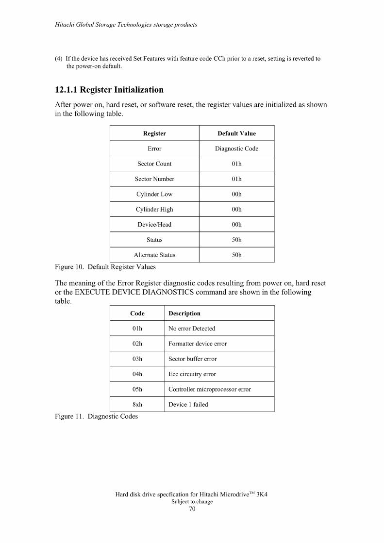
(4) If the device has received Set Features with feature code CCh prior to a reset, setting is reverted tothe power-on default.
12.1.1 Register InitializationAfter power on, hard reset, or software reset, the register values are initialized as shownin the following table.
50hAlternate Status
50hStatus
00hDevice/Head
00hCylinder High
00hCylinder Low
01hSector Number
01hSector Count
Diagnostic CodeError
Default ValueRegister
Figure 10. Default Register Values
The meaning of the Error Register diagnostic codes resulting from power on, hard resetor the EXECUTE DEVICE DIAGNOSTICS command are shown in the followingtable.
Device 1 failed8xh
Controller microprocessor error05h
Ecc circuitry error04h
Sector buffer error03h
Formatter device error02h
No error Detected01h
DescriptionCode
Figure 11. Diagnostic Codes
Hitachi Global Storage Technologies storage products
Hard disk drive specfication for Hitachi MicrodriveTM 3K4 Subject to change
70
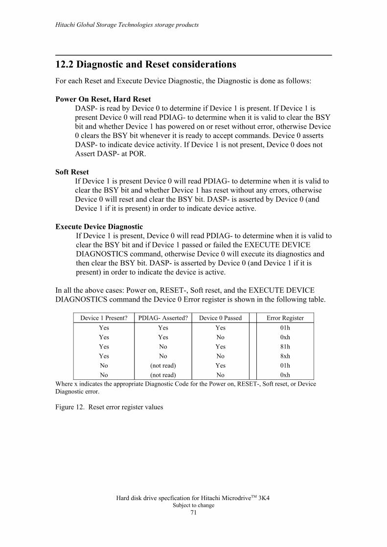
12.2 Diagnostic and Reset considerationsFor each Reset and Execute Device Diagnostic, the Diagnostic is done as follows:
Power On Reset, Hard ResetDASP- is read by Device 0 to determine if Device 1 is present. If Device 1 ispresent Device 0 will read PDIAG- to determine when it is valid to clear the BSYbit and whether Device 1 has powered on or reset without error, otherwise Device0 clears the BSY bit whenever it is ready to accept commands. Device 0 assertsDASP- to indicate device activity. If Device 1 is not present, Device 0 does notAssert DASP- at POR.
Soft ResetIf Device 1 is present Device 0 will read PDIAG- to determine when it is valid toclear the BSY bit and whether Device 1 has reset without any errors, otherwiseDevice 0 will reset and clear the BSY bit. DASP- is asserted by Device 0 (andDevice 1 if it is present) in order to indicate device active.
Execute Device DiagnosticIf Device 1 is present, Device 0 will read PDIAG- to determine when it is valid toclear the BSY bit and if Device 1 passed or failed the EXECUTE DEVICE DIAGNOSTICS command, otherwise Device 0 will execute its diagnostics andthen clear the BSY bit. DASP- is asserted by Device 0 (and Device 1 if it ispresent) in order to indicate the device is active.
In all the above cases: Power on, RESET-, Soft reset, and the EXECUTE DEVICE DIAGNOSTICS command the Device 0 Error register is shown in the following table.
0xhNo(not read)No01hYes(not read)No8xhNoNoYes81hYesNoYes0xhNoYesYes01hYesYesYes
Error RegisterDevice 0 PassedPDIAG- Asserted?Device 1 Present?
Where x indicates the appropriate Diagnostic Code for the Power on, RESET-, Soft reset, or DeviceDiagnostic error.
Figure 12. Reset error register values
Hitachi Global Storage Technologies storage products
Hard disk drive specfication for Hitachi MicrodriveTM 3K4 Subject to change
71
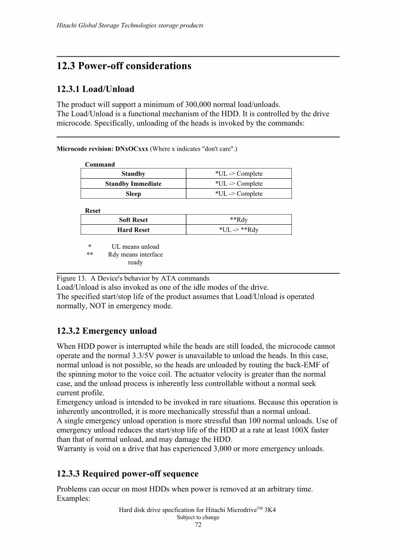
12.3 Power-off considerations
12.3.1 Load/UnloadThe product will support a minimum of 300,000 normal load/unloads.The Load/Unload is a functional mechanism of the HDD. It is controlled by the drivemicrocode. Specifically, unloading of the heads is invoked by the commands:
Microcode revision: DNxOCxxx (Where x indicates "don't care".)
Command
*UL -> CompleteSleep*UL -> CompleteStandby Immediate*UL -> CompleteStandby
Reset
*UL -> **RdyHard Reset**RdySoft Reset
Rdy means interfaceready
**UL means unload*
Figure 13. A Device's behavior by ATA commands Load/Unload is also invoked as one of the idle modes of the drive.The specified start/stop life of the product assumes that Load/Unload is operatednormally, NOT in emergency mode.
12.3.2 Emergency unloadWhen HDD power is interrupted while the heads are still loaded, the microcode cannotoperate and the normal 3.3/5V power is unavailable to unload the heads. In this case,normal unload is not possible, so the heads are unloaded by routing the back-EMF ofthe spinning motor to the voice coil. The actuator velocity is greater than the normalcase, and the unload process is inherently less controllable without a normal seekcurrent profile.Emergency unload is intended to be invoked in rare situations. Because this operation isinherently uncontrolled, it is more mechanically stressful than a normal unload.A single emergency unload operation is more stressful than 100 normal unloads. Use ofemergency unload reduces the start/stop life of the HDD at a rate at least 100X fasterthan that of normal unload, and may damage the HDD.Warranty is void on a drive that has experienced 3,000 or more emergency unloads.
12.3.3 Required power-off sequenceProblems can occur on most HDDs when power is removed at an arbitrary time.Examples:
Hitachi Global Storage Technologies storage products
Hard disk drive specfication for Hitachi MicrodriveTM 3K4 Subject to change
72
Data loss from the write buffer.If the drive is writing a sector, a partially-written sector with an incorrect ECCblock results. The sector contents are destroyed, and reading that sector results in ahard error.Heads possibly land in the data zone instead of landing zone, depending on thedesign of the HDD.
You may then turn off the HDD in the following order:I. Issue STANDBY IMMEDIATE command. ( STANDBY IMMEDIATE command
can be replaced by STANDBY or SLEEP command )II. Wait until Command Complete Status is returned. (It may take up to 350 ms in
typical case) III. Terminate power to HDD.
This power-down sequence should be followed for entry into any system power-downstate, or system suspend state, or system hibernation state. In a robustly designedsystem, emergency unload is limited to rare scenarios such as battery removal duringoperation.
Hitachi Global Storage Technologies storage products
Hard disk drive specfication for Hitachi MicrodriveTM 3K4 Subject to change
73
12.4 Sector Addressing Mode
12.4.1 Logical CHS Addressing ModeThe logical CHS addressing is made up of three fields: the cylinder number, the headnumber and the sector number. Sectors are numbered from 1 to the maximum valueallowed by the current CHS translation mode but can not exceed 255(0FFh). Heads arenumbered from 0 to the maximum value allowed by the current CHS translation modebut can not exceed 15(0Fh). Cylinders are numbered from 0 to the maximum valueallowed by the current CHS translation mode but cannot exceed 65535(0FFFFh).When the host selects a CHS translation mode using the INITIALIZE DRIVEPARAMETERS command, the host requests the number of sectors per logical trackand the number of heads per logical cylinder. The device then computes the number oflogical cylinders available in requested mode.The current CHS translation mode, as well as the default CHS translation mode, isreturned by the Identify Device Information.
12.4.2 LBA Addressing ModeLogical sectors on the device shall be linearly mapped with the first LBA addressedsector (sector 0) being the same sector as the first logical CHS addressed sector (cylinder 0, head 0, sector 1). Irrespective of the logical CHS translation mode currentlyin effect, the LBA address of a given logical sector does not change. The following isalways true:
LBA = ( (cylinder * heads_per_cylinder + heads) * sectors_per_track ) + sector - 1where heads_per_cylinder and sectors_per_track are the current translation modevalues.
On LBA addressing mode, the LBA value is set to the following register.
7- 0LBA bits<---Sector Number15- 8LBA bits<---Cylinder Low23-16LBA bits<---Cylinder High27-24LBA bits<---Device/Head
Hitachi Global Storage Technologies storage products
Hard disk drive specfication for Hitachi MicrodriveTM 3K4 Subject to change
74
12.5 Power Management FeatureThe power management feature set permits a host to modify the behavior in a mannerwhich reduces the power required to operate. The power management feature setprovides a set of commands and a timer that enables a device to implement low powerconsumption modes. implement the following set of functions.
I. A Standby timerII. IDLE commandIII. IDLE IMMEDIATE commandIV. STANDBY commandV. STANDBY IMMEDIATE command
12.5.1 Power Mode
The device is in execution of a command or accessing the disk media with readlook-ahead function or write cache function.
Active Mode
Refer to the section of Adoptive Battery Life Extender Feature.Idle Mode
The device interface is capable of accepting commands, but as the media may notimmediately accessible, there is a delay while waiting for the spindle to reach operatingspeed.
StandbyMode
12.5.2 Power Management CommandsThe CHECK POWER MODE command allows a host to determine if a device iscurrently in, going to or leaving standby mode.The IDLE and IDLE IMMEDIATE commands move a device to idle mode immediatelyfrom the active or standby modes. The IDLE command also sets the standby timer countand starts the standby timer.The STANDBY and STANDBY IMMEDIATE commands move a device to standbymode immediately from the active or idle modes. The STANDBY command also setsthe standby timer count.
12.5.3 STANDBY command completion timingI. Confirm the completion of writing cached data in the buffer to mediaII. Unload heads on the rampIII. Set DRDY bit and DSC bit in Status RegisterIV. Set INTRQ (completion of the command)V. Activate the spindle break to stop the spindle motorVI. Wait until spindle motor is stoppedVII. Perform post process
Hitachi Global Storage Technologies storage products
Hard disk drive specfication for Hitachi MicrodriveTM 3K4 Subject to change
75
12.5.4 Standby timerThe standby timer provides a method for the device to automatically enter standbymode from either active or idle mode following a host programmed period of inactivity.If the device is in the active or idle mode, the device waits for the specified time periodand if no command is received, the device automatically enters the standby mode.If the value of SECTOR COUNT register on IDLE command or STANDBY commandis set to 00h, the device will automatically set the standby timer to 109 minutes. If theadvanced power management level is less than 80h, which is power-on default, thetransition timing to enter Standby mode is determined by either standby timer orAdaptive Battery Life Extender algorithm, whichever meets the condition first.
12.5.5 StatusIn the active, idle and standby modes, the device shall have RDY bit of the statusregister set. If BSY bit is not set, device shall be ready to accept any command.
12.5.6 Interface Capability for Power ModesEach power mode affects the physical interface as defined in the following table:
InactiveYes10SleepInactiveYes10StandbyActiveYes10IdleActiveYesxxActiveMediaInterface activeRDYBSYMode
Figure 14. Power conditions
Ready(RDY) is not a power condition. A device may post ready at the interface eventhough the media may not be accessible.
12.5.7 Initial Power Mode at Power OnThe device power up in Standby mode.
Hitachi Global Storage Technologies storage products
Hard disk drive specfication for Hitachi MicrodriveTM 3K4 Subject to change
76

12.6 Advanced Power Management (Adaptive Battery LifeExtender 3) Feature
This feature provides power saving without performance degradation. The AdaptiveBattery Life Extender 3 (ABLE-3) technology intelligently manages transition amongpower modes within the device by monitoring access patterns of the host.This technology has three idle modes; Performance Idle mode, Active Idle mode, andLow Power Idle mode.
This feature allows the host to select an advanced power management level. Theadvanced power management level is a scale from the lowest power consumptionsetting of 01h to the maximum performance level of FEh. Device performance mayincrease with increasing advanced power management levels. Device powerconsumption may increase with increasing advanced power management levels. Theadvanced power management levels contain discrete bands, described in the section ofSET FEATURE command in detail.This feature set uses the following functions:
A SET FEATURES subcommand to enable Advanced Power ManagementA SET FEATURES subcommand to disable Advanced Power Management
The Advanced Power Management feature is independent of the Standby timer setting.If both Advanced Power Management level and the Standby timer are set, the devicewill goto the Standby state when the timer times out or the device's Advanced PowerManagement algorithm indicates that it is time to enter the Standby state.The IDENTIFY DEVICE response word 83, bit 3 indicates that Advanced PowerManagement feature is supported if set. Word 86, bit 3 indicates that Advanced PowerManagement is enabled if set.Word 96, bits 7-0 contain the current Advanced Power Management level if AdvancedPower Management is enabled.
12.6.1 Performance Idle modeThis mode is usually entered immediately after Active mode command processing iscomplete, instead of conventional idle mode. In Performance Idle mode, all electroniccomponents remain powered and full frequency servo remains operational. Thisprovides instantaneous response to the next command. The duration of this mode isintelligently managed as described below.
12.6.2Active Idle modeIn this mode, power consumption is 45-55% less than that of Performance Idle mode.Additional electronics are powered off, and the head is prked near the mid-diameterwithout servoing. Recovery time to Active mode is about 10ms.
Hitachi Global Storage Technologies storage products
Hard disk drive specfication for Hitachi MicrodriveTM 3K4 Subject to change
77
12.6.3 Low Power Idle modePower consumption is 55%-65% less than that of Performance Idle mode. The heads areunloaded on the ramp, however the spindle is still rotated at the full speed. Recoverytime to Active mode is about 300ms.
12.6.4 Transition TimeThe transition time is dynamically managed by users recent access pattern, instead offixed times. The ABLE-3 algorithm monitors the interval between commands instead ofthe command frequency of ABLE-2. The algorithm supposes that next command willcome with the same command interval distribution as the previous access pattern. Thealgorithm calculates the expected average saving energy and response delay for nextcommand in several transition time case based on this assumption. And it selects themost effective transition time with the condition that the calculated response delay isshorter than the value calculated from the specifid level by SET FEATURE ENABLEADAPTIVE POWER MANAGEMENT command.The optimal time to enter Active Idle mode is variable depending on the users recentbehavior. It is not possible to achieve the same level of Power savings with a fixed entrytime into Performance Idle because every users data and access pattern is different. Theoptimum entry time changes over time.The same algorithm works for entering into Low Power Idle mode and Standby mode,which consumes less power but need more recovery time switching from this mode toActive mode.
Hitachi Global Storage Technologies storage products
Hard disk drive specfication for Hitachi MicrodriveTM 3K4 Subject to change
78
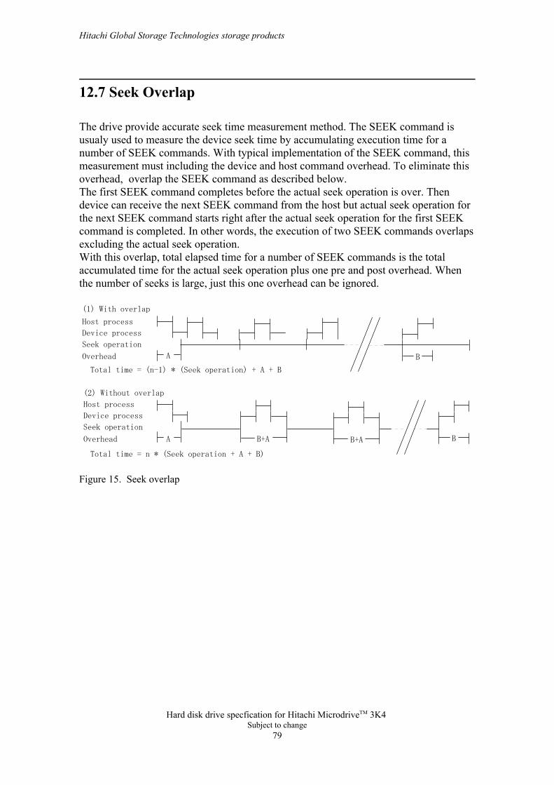
12.7 Seek Overlap
The drive provide accurate seek time measurement method. The SEEK command isusualy used to measure the device seek time by accumulating execution time for anumber of SEEK commands. With typical implementation of the SEEK command, thismeasurement must including the device and host command overhead. To eliminate thisoverhead, overlap the SEEK command as described below.The first SEEK command completes before the actual seek operation is over. Thendevice can receive the next SEEK command from the host but actual seek operation forthe next SEEK command starts right after the actual seek operation for the first SEEKcommand is completed. In other words, the execution of two SEEK commands overlapsexcluding the actual seek operation.With this overlap, total elapsed time for a number of SEEK commands is the total accumulated time for the actual seek operation plus one pre and post overhead. Whenthe number of seeks is large, just this one overhead can be ignored.
Figure 15. Seek overlap
Hitachi Global Storage Technologies storage products
Hard disk drive specfication for Hitachi MicrodriveTM 3K4 Subject to change
79
(1) With overlap
(2) Without overlap
Host process
Host process
Device process
Device process
Seek operation
Seek operation
Overhead
Overhead
A
A B+A
B
B+A B
Total time = (n-1) * (Seek operation) + A + B
Total time = n * (Seek operation + A + B)
12.8 Write Cache FunctionWrite cache is a performance enhancement whereby the device reports completion ofthe write command (WRITE SECTORS, WRITE MULTIPLE, WRITE SECTORSWITHOUT ERASE, WRITE MULTIPLE WITHOUT ERASE, WRITE DMA, WRITEVERIFY ) to the host as soon as the device has received all of the data into its buffer.The device assumes responsibility to write the data subsequently onto the disk.
While writing data after completed acknowledgment of a write command, soft resetor hard reset does not affect its operation. But power off terminates writingoperation immediately and unwritten data are to be lost.
FLUSH CACHE, SOFT RESET, STANDBY, STANDBY IMMEDIATE andSLEEP are executed after the completion of writing to disk media on enabling writecache function. So the host system can confirm the completion of write cacheoperation by issuing FLUSH CACHE command, SOFT RESET, STANDBYcommand, STANDBY IMMEDIATE command and SLEEP command, and then, byconfirming its completion.
The retry bit of WRITE SECTORS is ignored when write cache is enabled.
Hitachi Global Storage Technologies storage products
Hard disk drive specfication for Hitachi MicrodriveTM 3K4 Subject to change
80
12.9 Reassign FunctionThe Reassign Function is used with read commands and write commands. The sectorsof data for reassignment are prepared as the spare data sector. The number of the sparesector's entry is 2026 entries. The one entry can register 256 consecutive sectorsmaximally.
This reassignment information is registered internally, and the information is availableright after completing the reassign function. Also the information is used on the nextpower on reset or hard reset.
If the number of the spare sector reaches 0 sector, the reassign function will be disabledautomatically.
The spare tracks for reassignment are located at regular interval. As a result ofreassignment, the physical location of logically sequenced sectors will be dispersed.
12.9.1 Auto Reassign FunctionThe sectors that show some errors may be reallocated automatically when specificconditions are met. The spare sectors for reallocation are located at reserved area. Theconditions for auto-reallocation are described below.
Non recovered write errors
When a write operation can not be completed after the Error Recovery Procedure(ERP)is fully carried out, the sector(s) are reallocated to the spare location. An error isreported to the host system only when the write cache is disabled and the autoreallocation fails.
If the number of available spare sectors reaches 16 sectors, the write cache function willbe disabled automatically.
If the command is without retry and the write cache function is disabled, the autoreassign function is not invoked.
Non recovered read errors
When a read operation fails after defined ERP is fully carried out, a hard error isreported to the host system. This location is registerred internally as a candidate for thereallocation. When a registerred location is specified as a target of a write operation, asequence of media verification is performed automatically. When the result of thisverification meets the criteria, this sector is reallocated.
Recovered read errors
When a read operation for a sector failed once then recovered at the specific ERP step,this sector of data is reallocated automatically. A media verification sequence may berun prior to the relocation according to the pre-defined conditions.
Hitachi Global Storage Technologies storage products
Hard disk drive specfication for Hitachi MicrodriveTM 3K4 Subject to change
81
12.10 Metadata Storage Function
Metadata storage is a small, non-volatile user area which address space is logicallyseparated from the main storage. The host can use metadata storage to store informationon the data contents itself, e.g, available free blocks, device properties, or any summaryinformation. The first implementation of metadata storage in the drive provides just32-bytes, but the command set design does not preclude any future enhancement. The metadata concept itself is not bound to any specific physical medium, although thedrive's metadata storage has one important property for rotating devices: the host canaccess metadata without rotating the disk. This medium property is expected tosupplement the applicability of the drive for the digital appliance.
12.10.1 Meatadata Storage Command SetAll metadata commands use command code B8h. Each command is specified as asubcommand of command B8h with Features Register containing the subcommandcode. Cylinder Low and High registers are used to specify metadata block address in512-byte unit, which ranges from 0 to [metadata capacity in bytes + 2] / 512. TheHitachi drive provides 32 bytes of metadata capacity; thus the valid address for theHitachi drive is 0000h only. Sector Count Register is used to specify the number ofblocks transferred between the host and the device. Sector Number Register is reservedand must be 00h for future use. Inquiry Metadata Media, which uses subcommand code 02h, returns 1 sector of datacontaining information on the device's metadata storage. Read Metadata, which usessubcommand code 03h, can read metadata contents. Inquiry Metadata Media and ReadMetadata return a status word that indicates whether the main storage contents havebeen modified since the last Write Metadata. The host can use the status word to checkif metadata is not consistent with the main storage contents. Write Metadata, which usessubcommand code 04h. can write metadata. The device does not interpret metadataitself, though it is recommended the first 10 bytes of metadata be a unique number thatsignifies the identity of remaining. In addition to define new command set, Identify Device is enhanced to use word 161as a capability bitstrip for CF command set extensions, which indicates support for themetadata command set. Details of command description are refered to "6.5 CF-ATA Command Description".
Hitachi Global Storage Technologies storage products
Hard disk drive specfication for Hitachi MicrodriveTM 3K4 Subject to change
82
13 Command ProtocolThe commands are grouped into different classes according to the protocols followedfor command execution. The command classes with their associated protocols aredefined below.
For all commands, the host must first check if BSY=1, and should proceed no furtherunless and until BSY=0. For all commands, the host must also wait for RDY=1 beforeproceeding.
A device must maintain either BSY=1 or DRQ=1 at all times until the command iscompleted. The INTRQ signal is used by the device to signal most, but not all, timeswhen the BSY bit is changed from 1 to 0 during command execution.
A command shall only be interrupted with a hardware or software reset. The result ofwriting to the Command register while BSY=1 or DRQ=1 is unpredictable and mayresult in data corruption. A command should only be interrupted by a reset at timeswhen the host thinks there may be a problem, such as a device that is no longerresponding.
Interrupts are cleared when the host reads the Status Register, issues a reset, or writes tothe Command Register.
13.1 Data In CommandsThese commands are:
Identify DeviceRead BufferRead LongRead MultipleRead Sectors
Execution includes the transfer of one or more 512 byte (>512 bytes on Read Long)sectors of data from the device to the host.
The device sets BSY=1 and prepares for data transfer.a.For the Read Long command:4.
The device sets DRQ=0 after the sector (or block)has been transferred to the host.f.The host reads one sector (or block) of data via the Data Register.e.The device clears the interrupt in response to the Status Register being read.d.In response to the interrupt, the host reads the Status Register.c.
When a sector (or block) of data is available for transfer to the host, the device sets BSY=0, setsDRQ=1, and interrupts the host.
b.The device sets BSY=1 and prepares for data transfer.a.
For each sector (or block) of data to be transferred:3.The host writes the command code to the Command Register.2.
The host writes any required parameters to the Features, Sector Count, Sector Number, Cylinder, andDevice/Head Registers.
1.
Hitachi Global Storage Technologies storage products
Hard disk drive specfication for Hitachi MicrodriveTM 3K4 Subject to change
83
The device sets DRQ=0 after the sector has been transferred to the host.f.The host reads the sector of data including ECC bytes via the Data Register.e.The device clears the interrupt in response to the Status Register being read.d.In response to the interrupt, the host reads the Status Register.c.
When the sector of data is available for transfer to the host, the device sets BSY=0, sets DRQ=1,and interrupts the host.
b.
The Read Multiple command transfers one block of data for each interrupt. The othercommands transfer one sector of data for each interrupt.
Note that the status data for a sector of data is available in the Status Register before thesector is transferred to the host.
If the device detects an invalid parameter, then it will abort the command by settingBSY=0, ERR=1, ABT=1, and interrupting the host.
If an error occurs, the device will set BSY=0, ERR=1, and DRQ=1. The device willthen store the error status in the Error Register, and interrupt the host. The registers willcontain the location of the sector in error. The errored location will be reported withCHS mode or LBA mode, the mode is decided by mode select bit (bit 6) ofDevice/Head register on issuing the command.
If an Uncorrectable Data Error (UNC=1) occurs, the defective data will be transferredfrom the media to the sector buffer, and will be available to be transferred to the host, atthe host's option. In case of Read Multiple command, the host should complete transferthe block which includes the error from the sector buffer and terminate whatever kind oftype of error occurred.
All data transfers to the host through the Data Register are 16 bits, except for the ECCbytes, which are 8 bits.
Hitachi Global Storage Technologies storage products
Hard disk drive specfication for Hitachi MicrodriveTM 3K4 Subject to change
84
13.2 Data Out CommandsThese commands are:
Format TrackWrite BufferWrite LongWrite MultipleWrite SectorsWrite Verify
Execution includes the transfer of one or more 512 byte (>512 bytes on Write Long)sectors of data from the host to the device.
The device clears the interrupt in response to the Status Register being read.f.In response to the interrupt, the host reads the Status Register.e.After processing the sector of data the device sets BSY=0 and interrupts the host.d.The device sets BSY=1 after it has received the sector.c.The host writes one sector of data including ECC bytes via the Data Register.b.The device sets BSY=0 and DRQ=1 when it is ready to receive a sector.a.
For the Write Long command:5.The device clears the interrupt in response to the Status Register being read.f.In response to the interrupt, the host reads the Status Register.e.
When the device has finished processing the sector (or block), it sets BSY=0, and interrupts thehost.
d.The device sets BSY=1 after it has received the sector (or block).c.The host writes one sector (or block) of data via the Data Register.b.The device sets BSY=0 and DRQ=1 when it is ready to receive a sector (or block).a.
For each sector (or block) of data to be transferred:4.The device sets BSY=1.3.The host writes the command code to the Command Register.2.
The host writes any required parameters to the Features, Sector Count, Sector Number, Cylinder, andDevice/Head Registers.
1.
The Write Multiple command transfers one block of data for each interrupt. The othercommands transfer one sector of data for each interrupt.
If the device detects an invalid parameter, then it will abort the command by settingBSY=0, ERR=1, ABT=1, and interrupting the host.
If an uncorrectable error occurs, the device will set BSY=0 and ERR=1, store the errorstatus in the Error Register, and interrupt the host. The registers will contain thelocation of the sector in error. The errored location will be reported with CHS mode orLBA mode. The mode is decided by mode select bit (bit 6) of Device/Head register onissuing the command.
All data transfers to the device through the Data Register are 16 bits, except for theECC bytes, which are 8 bits.
Hitachi Global Storage Technologies storage products
Hard disk drive specfication for Hitachi MicrodriveTM 3K4 Subject to change
85
13.3 Non-Data CommandsThese commands are:
Check Power ModeEnable/Disable Delayed WriteErase sectorsExecute Device DiagnosticFlush CacheFormat UnitIdleIdle ImmediateInitialize Device ParametersRead Verify SectorsRecalibrateSecurity Erase PrepareSeekSense conditionSet FeaturesSet Multiple ModeSleepStandbyStandby Immediate
Execution of these commands involves no data transfer.
I. The host writes any required parameters to the Features, Sector Count, SectorNumber, Cylinder, and Device/Head Registers.
II. The host writes the command code to the Command Register.III. The device sets BSY=1.IV. When the device has finished processing the command, it sets BSY=0, and
interrupts the host.V. In response to the interrupt, the host reads the Status Register.VI. The device clears the interrupt in response to the Status Register being read.
Hitachi Global Storage Technologies storage products
Hard disk drive specfication for Hitachi MicrodriveTM 3K4 Subject to change
86
13.4 DMA Data Transfer CommandsThe drive supports DMA Data Transfer Commands ONLY in True IDE mode.
These commands are:
Read DMAWrite DMA
Data transfer using DMA commands differ in two ways from PIO transfers:
data transfers are performed using the slave-DMA channelno intermediate sector interrupts are issued on multi-sector commands
Initiation of the DMA transfer commands is identical to the Read Sector or Write Sectorcommands except that the host initializes the slave-DMA channel prior to issuing thecommand.
The interrupt handler for DMA transfers is different in that:
no intermediate sector interrupts are issued on multi-sector commandsthe host resets the DMA channel prior to reading status from the device.
The DMA protocol allows high performance multi-tasking operating systems toeliminate processor overhead associated with PIO transfers.
I. Host initializes the slave-DMA channelII. Host writes any required parameters to the Features, Sector Count, Sector Number,
Cylinder and Device/Head registers.III. Host writes command code to the Command RegisterIV. The device sets DMARQ when it is ready to transfer any part of the data.V. Host transfers the data using the DMA transfer protocol currently in effect.VI. When all of the data has been transferred, the device generates an interrupt to the
host.VII. Host resets the slave-DMA channelVIII.Host reads the Status Register and, optionally, the Error Register
Hitachi Global Storage Technologies storage products
Hard disk drive specfication for Hitachi MicrodriveTM 3K4 Subject to change
87
13.4.1 Access Metadata Storage - B8h
...See Below...Status00011101Command
--------Device/Head----D1-1Device/Head
--------Cylinder High--------Cylinder High
--------Cylinder Low--------Cylinder Low
--------Sector Number--------Sector Number
V-------Sector Count10000000Sector Count
...See Below...ErrorVVVVVVVVFeature
--------Data--------Data
01234567Register01234567RegisterCommand Block Input RegistersCommand Block Output Registers
V00--00000V00000ERRIDXCORDRQDSCDFRDYBSYAMNT0NABT0IDN0UNCCRC
0123456701234567Status RegisterError Register
Figure 16. Access Metadata Storage Command (B8h)
This command accesses metadata storage area.Following subcommand are supported and specified with Feature Register value.
Write Metadata Storage04h
Read Metadata Storage03h
Inquiry Metadata Storage02h
OperationFeature
Figure 17. Supported subcommand
Inquiry Metadata Storage (subcommand code - 02h) enables host to read capacity of thedevice's Metadata Storage along with information associated with the charasteristics of theMetadata Storage. The data returned from the device is in following format.
media status word bit 0: 1 = content changed 0 = content not changed bit 1-15: reserved
000xh2
media property bit 0: 1 = rotating, 0 = silicon bit 1-15: reserved
0000h1data format revision0001h0
Descriptiondataword
Hitachi Global Storage Technologies storage products
Hard disk drive specfication for Hitachi MicrodriveTM 3K4 Subject to change
88
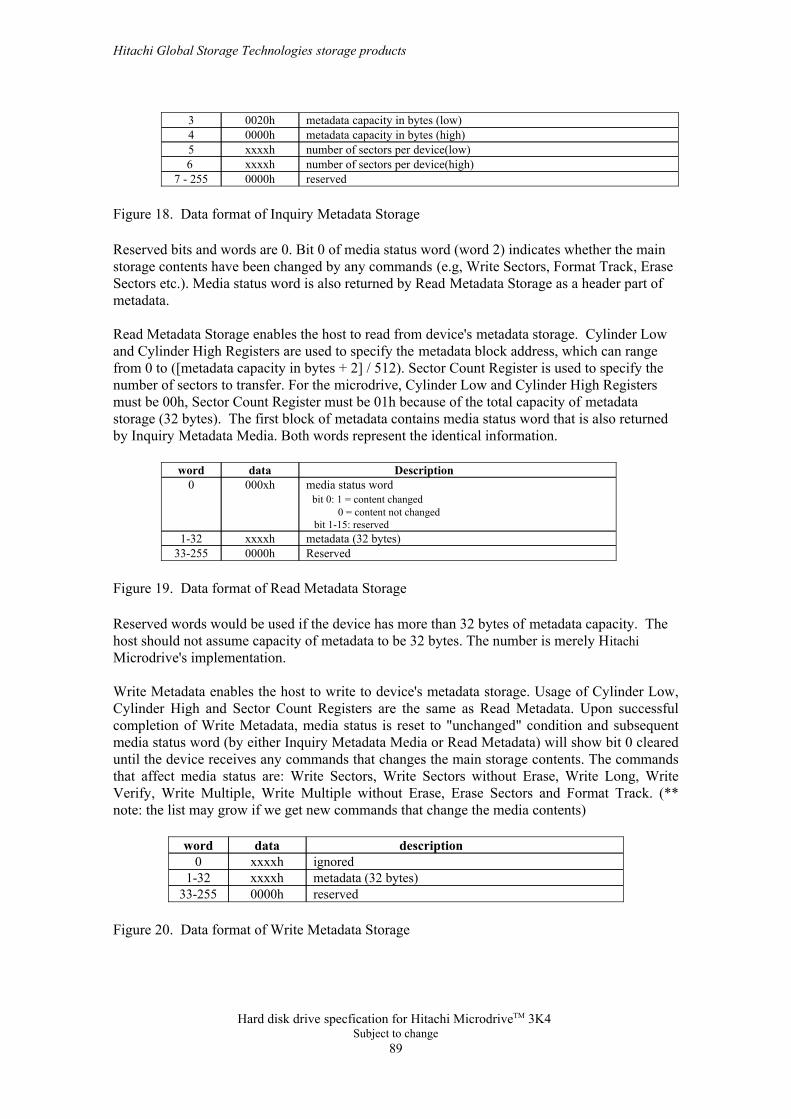
reserved0000h7 - 255number of sectors per device(high)xxxxh6 number of sectors per device(low)xxxxh5metadata capacity in bytes (high)0000h4metadata capacity in bytes (low)0020h3
Figure 18. Data format of Inquiry Metadata Storage
Reserved bits and words are 0. Bit 0 of media status word (word 2) indicates whether the mainstorage contents have been changed by any commands (e.g, Write Sectors, Format Track, EraseSectors etc.). Media status word is also returned by Read Metadata Storage as a header part ofmetadata.
Read Metadata Storage enables the host to read from device's metadata storage. Cylinder Lowand Cylinder High Registers are used to specify the metadata block address, which can rangefrom 0 to ([metadata capacity in bytes + 2] / 512). Sector Count Register is used to specify thenumber of sectors to transfer. For the microdrive, Cylinder Low and Cylinder High Registersmust be 00h, Sector Count Register must be 01h because of the total capacity of metadatastorage (32 bytes). The first block of metadata contains media status word that is also returnedby Inquiry Metadata Media. Both words represent the identical information.
Reserved0000h33-255metadata (32 bytes)xxxxh1-32
media status word bit 0: 1 = content changed 0 = content not changed bit 1-15: reserved
000xh0Descriptiondataword
Figure 19. Data format of Read Metadata Storage
Reserved words would be used if the device has more than 32 bytes of metadata capacity. Thehost should not assume capacity of metadata to be 32 bytes. The number is merely HitachiMicrodrive's implementation.
Write Metadata enables the host to write to device's metadata storage. Usage of Cylinder Low,Cylinder High and Sector Count Registers are the same as Read Metadata. Upon successfulcompletion of Write Metadata, media status is reset to "unchanged" condition and subsequentmedia status word (by either Inquiry Metadata Media or Read Metadata) will show bit 0 cleareduntil the device receives any commands that changes the main storage contents. The commandsthat affect media status are: Write Sectors, Write Sectors without Erase, Write Long, WriteVerify, Write Multiple, Write Multiple without Erase, Erase Sectors and Format Track. (**note: the list may grow if we get new commands that change the media contents)
reserved0000h33-255metadata (32 bytes)xxxxh1-32ignoredxxxxh0
descriptiondataword
Figure 20. Data format of Write Metadata Storage
Hitachi Global Storage Technologies storage products
Hard disk drive specfication for Hitachi MicrodriveTM 3K4 Subject to change
89
Word 0 is a pad and metadata starts with the word 1. Reserved words would be used if thedevice has more than 32 bytes of metadata capacity. The host should not assume capacity ofmetadata to be 32 bytes. The number is merely Hitachi Microdrive's implementation.
Hitachi Global Storage Technologies storage products
Hard disk drive specfication for Hitachi MicrodriveTM 3K4 Subject to change
90
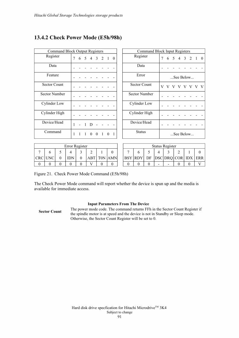
13.4.2 Check Power Mode (E5h/98h)
...See Below...Status10100111Command
--------Device/Head----D1-1Device/Head
--------Cylinder High--------Cylinder High
--------Cylinder Low--------Cylinder Low
--------Sector Number--------Sector Number
VVVVVVVVSector Count--------Sector Count
...See Below...Error--------Feature
--------Data--------Data
01234567Register01234567RegisterCommand Block Input RegistersCommand Block Output Registers
V00--00000V00000ERRIDXCORDRQDSCDFRDYBSYAMNT0NABT0IDN0UNCCRC
0123456701234567Status RegisterError Register
Figure 21. Check Power Mode Command (E5h/98h)
The Check Power Mode command will report whether the device is spun up and the media isavailable for immediate access.
The power mode code. The command returns FFh in the Sector Count Register ifthe spindle motor is at speed and the device is not in Standby or Sleep mode.Otherwise, the Sector Count Register will be set to 0.
Sector Count
Input Parameters From The Device
Hitachi Global Storage Technologies storage products
Hard disk drive specfication for Hitachi MicrodriveTM 3K4 Subject to change
91
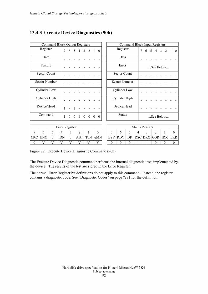
13.4.3 Execute Device Diagnostics (90h)
...See Below...Status00001001Command
--------Device/Head-----1-1Device/Head
--------Cylinder High--------Cylinder High
--------Cylinder Low--------Cylinder Low
--------Sector Number--------Sector Number
--------Sector Count--------Sector Count
...See Below...Error--------Feature
--------Data--------Data
01234567Register01234567RegisterCommand Block Input RegistersCommand Block Output Registers
000--000VVVVVVV0ERRIDXCORDRQDSCDFRDYBSYAMNT0NABT0IDN0UNCCRC
0123456701234567Status RegisterError Register
Figure 22. Execute Device Diagnostic Command (90h)
The Execute Device Diagnostic command performs the internal diagnostic tests implemented bythe device. The results of the test are stored in the Error Register.
The normal Error Register bit definitions do not apply to this command. Instead, the registercontains a diagnostic code. See "Diagnostic Codes" on page ??71 for the definition.
Hitachi Global Storage Technologies storage products
Hard disk drive specfication for Hitachi MicrodriveTM 3K4 Subject to change
92
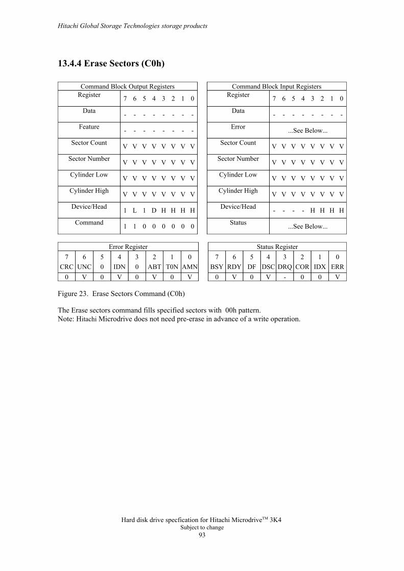
13.4.4 Erase Sectors (C0h)
...See Below...Status00000011Command
HHHH----Device/HeadHHHHD1L1Device/Head
VVVVVVVVCylinder HighVVVVVVVVCylinder High
VVVVVVVVCylinder LowVVVVVVVVCylinder Low
VVVVVVVVSector NumberVVVVVVVVSector Number
VVVVVVVVSector CountVVVVVVVVSector Count
...See Below...Error--------Feature
--------Data--------Data
01234567Register01234567RegisterCommand Block Input RegistersCommand Block Output Registers
V00-V0V0V0V0V0V0ERRIDXCORDRQDSCDFRDYBSYAMNT0NABT0IDN0UNCCRC
0123456701234567Status RegisterError Register
Figure 23. Erase Sectors Command (C0h)
The Erase sectors command fills specified sectors with 00h pattern.Note: Hitachi Microdrive does not need pre-erase in advance of a write operation.
Hitachi Global Storage Technologies storage products
Hard disk drive specfication for Hitachi MicrodriveTM 3K4 Subject to change
93
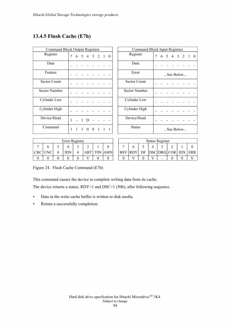
13.4.5 Flush Cache (E7h)
...See Below...Status11100111Command
--------Device/Head----D1-1Device/Head
--------Cylinder High--------Cylinder High
--------Cylinder Low--------Cylinder Low
--------Sector Number--------Sector Number
--------Sector Count--------Sector Count
...See Below...Error--------Feature
--------Data--------Data
01234567Register01234567RegisterCommand Block Input RegistersCommand Block Output Registers
V00-V0V000V00000ERRIDXCORDRQDSCDFRDYBSYAMNT0NABT0IDN0UNCCRC
0123456701234567Status RegisterError Register
Figure 24. Flush Cache Command (E7h)
This command causes the device to complete writing data from its cache.
The device returns a status, RDY=1 and DSC=1 (50h), after following sequence.
Data in the write cache buffer is written to disk media.
Return a successfully completion.
Hitachi Global Storage Technologies storage products
Hard disk drive specfication for Hitachi MicrodriveTM 3K4 Subject to change
94
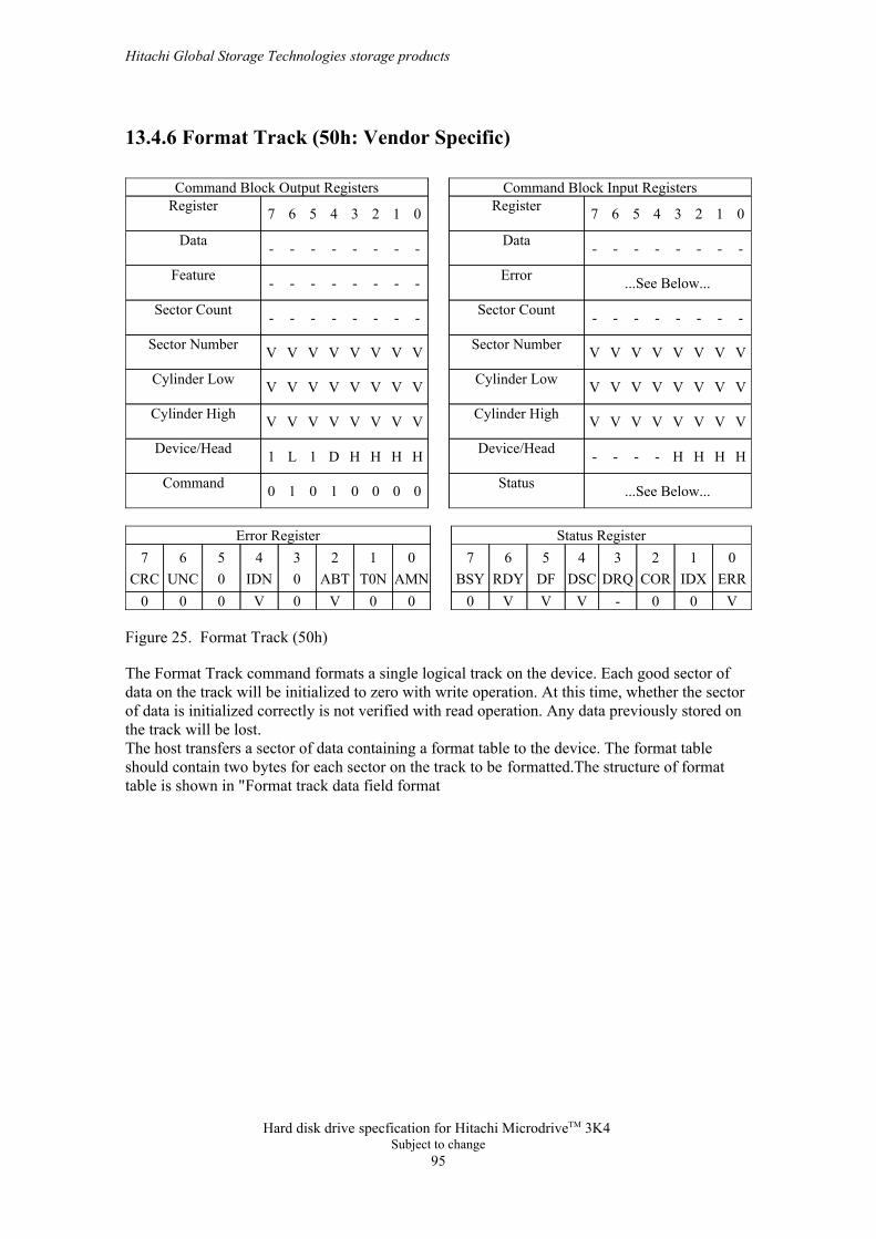
13.4.6 Format Track (50h: Vendor Specific)
...See Below...Status00001010Command
HHHH----Device/HeadHHHHD1L1Device/Head
VVVVVVVVCylinder HighVVVVVVVVCylinder High
VVVVVVVVCylinder LowVVVVVVVVCylinder Low
VVVVVVVVSector NumberVVVVVVVVSector Number
--------Sector Count--------Sector Count
...See Below...Error--------Feature
--------Data--------Data
01234567Register01234567RegisterCommand Block Input RegistersCommand Block Output Registers
V00-VVV000V0V000ERRIDXCORDRQDSCDFRDYBSYAMNT0NABT0IDN0UNCCRC
0123456701234567Status RegisterError Register
Figure 25. Format Track (50h)
The Format Track command formats a single logical track on the device. Each good sector ofdata on the track will be initialized to zero with write operation. At this time, whether the sectorof data is initialized correctly is not verified with read operation. Any data previously stored onthe track will be lost.The host transfers a sector of data containing a format table to the device. The format tableshould contain two bytes for each sector on the track to be formatted.The structure of formattable is shown in "Format track data field format
Hitachi Global Storage Technologies storage products
Hard disk drive specfication for Hitachi MicrodriveTM 3K4 Subject to change
95
" on page 99. The first byte should contain a descriptor value and the second byte shouldcontain the sector number. The descriptor value should be 0 for a good sector, and any otherdescriptor value will cause an aborted error. The remaining bytes of the sector following theformat table are ignored.Since device performance is optimal at 1:1 interleave, and the device uses relative blockaddressing internally, the device will always format a track in the same way no matter whatsector numbering is specified in the format table.
Hitachi Global Storage Technologies storage products
Hard disk drive specfication for Hitachi MicrodriveTM 3K4 Subject to change
96
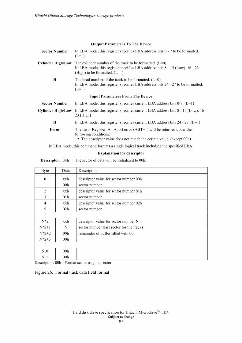
The sector of data will be initialized to 00h.Descriptor : 00h
Explanation for descriptor
In LBA mode, this command formats a single logical track including the specified LBA.
The Error Register. An Abort error (ABT=1) will be returned under thefollowing conditions:
The descriptor value does not match the certain value. (except 00h)
Error
In LBA mode, this register specifies current LBA address bits 24 - 27. (L=1)H
In LBA mode, this register specifies current LBA address bits 8 - 15 (Low), 16 -23 (High)
Cylinder High/Low
In LBA mode, this register specifies current LBA address bits 0-7. (L=1)Sector Number
Input Parameters From The Device
The head number of the track to be formatted. (L=0)In LBA mode, this register specifies LBA address bits 24 - 27 to be formatted.(L=1)
H
The cylinder number of the track to be formatted. (L=0)In LBA mode, this register specifies LBA address bits 8 - 15 (Low), 16 - 23(High) to be formatted. (L=1)
Cylinder High/Low
In LBA mode, this register specifies LBA address bits 0 - 7 to be formatted.(L=1)
Sector Number
Output Parameters To The Device
00h51100h510
::00hN*2+3
remainder of buffer filled with 00h00hN*2+2sector number (last sector for the track)NN*2+1descriptor value for sector number NxxhN*2
::sector number02h5descriptor value for sector number 02hxxh4sector number01h3descriptor value for sector number 01hxxh2sector number00h1descriptor value for sector number 00hxxh0
DescriptionDataByte
Descriptor : 00h - Format sector as good sector
Figure 26. Format track data field format
Hitachi Global Storage Technologies storage products
Hard disk drive specfication for Hitachi MicrodriveTM 3K4 Subject to change
97
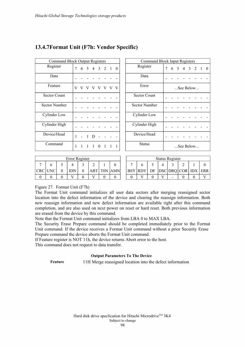
13.4.7Format Unit (F7h: Vendor Specific)
...See Below...Status11101111Command
--------Device/Head----D1-1Device/Head
--------Cylinder High--------Cylinder High
--------Cylinder Low--------Cylinder Low
--------Sector Number--------Sector Number
--------Sector Count--------Sector Count
...See Below...ErrorVVVVVVVVFeature
--------Data--------Data
01234567Register01234567RegisterCommand Block Input RegistersCommand Block Output Registers
V00-V0V000V0V000ERRIDXCORDRQDSCDFRDYBSYAMNT0NABT0IDN0UNCCRC
0123456701234567Status RegisterError Register
Figure 27. Format Unit (F7h) The Format Unit command initializes all user data sectors after merging reassigned sectorlocation into the defect information of the device and clearing the reassign information. Bothnew reassign information and new defect information are available right after this commandcompletion, and are also used on next power on reset or hard reset. Both previous informationare erased from the device by this command.Note that the Format Unit command initializes from LBA 0 to MAX LBA.The Security Erase Prepare command should be completed immediately prior to the FormatUnit command. If the device receives a Format Unit command without a prior Security Erase Prepare command the device aborts the Format Unit command.If Feature register is NOT 11h, the device returns Abort error to the host.This command does not request to data transfer.
11H Merge reassigned location into the defect informationFeatureOutput Parameters To The Device
Hitachi Global Storage Technologies storage products
Hard disk drive specfication for Hitachi MicrodriveTM 3K4 Subject to change
98

13.4.8Identify Device (ECh)
...See Below...Status00110111Command
--------Device/Head----D1-1Device/Head
--------Cylinder High--------Cylinder High
--------Cylinder Low--------Cylinder Low
--------Sector Number--------Sector Number
--------Sector Count--------Sector Count
...See Below...Error--------Feature
--------Data--------Data
01234567Register01234567RegisterCommand Block Input RegistersCommand Block Output Registers
V00--0V000V00000ERRIDXCORDRQDSCDFRDYBSYAMNT0NABT0IDN0UNCCRC
0123456701234567Status RegisterError Register
Figure 28. Identify Device Command (ECh)
The Identify Device command requests the device to transfer configuration information to thehost. The device will transfer a sector to the host containing the information in "" on page 1070TBD.
Hitachi Global Storage Technologies storage products
Hard disk drive specfication for Hitachi MicrodriveTM 3K4 Subject to change
99
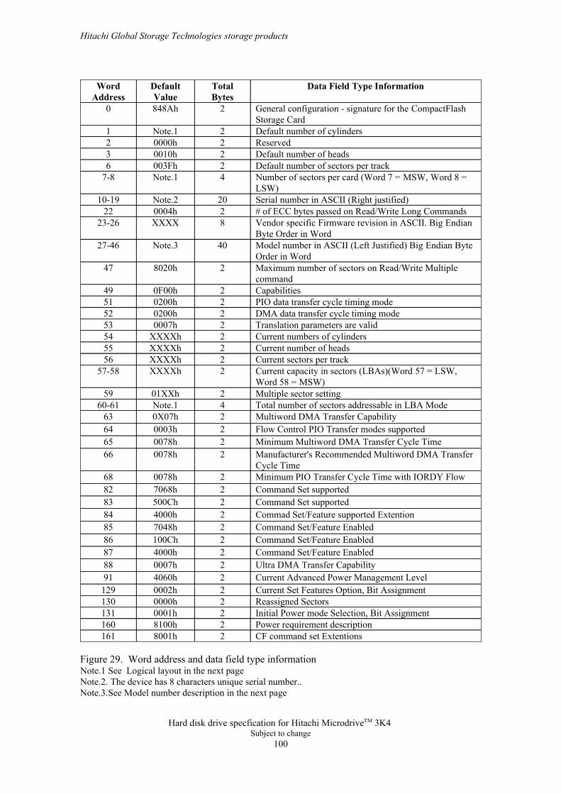
CF command set Extentions28001h161Power requirement description28100h160Initial Power mode Selection, Bit Assignment20001h131Reassigned Sectors20000h130Current Set Features Option, Bit Assignment20002h129Current Advanced Power Management Level24060h91Ultra DMA Transfer Capability20007h88Command Set/Feature Enabled24000h87Command Set/Feature Enabled2100Ch86Command Set/Feature Enabled27048h85Commad Set/Feature supported Extention24000h84Command Set supported2500Ch83Command Set supported27068h82Minimum PIO Transfer Cycle Time with IORDY Flow20078h68
Manufacturer's Recommended Multiword DMA TransferCycle Time
20078h66Minimum Multiword DMA Transfer Cycle Time20078h65Flow Control PIO Transfer modes supported20003h64Multiword DMA Transfer Capability20X07h63Total number of sectors addressable in LBA Mode4Note.160-61Multiple sector setting201XXh59
Current capacity in sectors (LBAs)(Word 57 = LSW,Word 58 = MSW)
2XXXXh57-58Current sectors per track2XXXXh56Current number of heads2XXXXh55Current numbers of cylinders2XXXXh54Translation parameters are valid20007h53DMA data transfer cycle timing mode20200h52PIO data transfer cycle timing mode20200h51Capabilities20F00h49
Maximum number of sectors on Read/Write Multiplecommand
28020h47
Model number in ASCII (Left Justified) Big Endian ByteOrder in Word
40Note.327-46
Vendor specific Firmware revision in ASCII. Big EndianByte Order in Word
8XXXX23-26# of ECC bytes passed on Read/Write Long Commands20004h22Serial number in ASCII (Right justified)20Note.210-19
Number of sectors per card (Word 7 = MSW, Word 8 =LSW)
4Note.17-8Default number of sectors per track2003Fh6Default number of heads20010h3Reserved20000h2Default number of cylinders2Note.11
General configuration - signature for the CompactFlashStorage Card
2848Ah0
Data Field Type InformationTotalBytes
DefaultValue
WordAddress
Figure 29. Word address and data field type informationNote.1 See Logical layout in the next pageNote.2. The device has 8 characters unique serial number.. Note.3.See Model number description in the next page
Hitachi Global Storage Technologies storage products
Hard disk drive specfication for Hitachi MicrodriveTM 3K4 Subject to change
100
word 0 : General ConfigurationThis field informs the device is a CompactFlash Storage Card.
word 1 : Default Number of Cylindersword 2 : Default Number of Headsword 6 : Default Number of Sectors per Trackword 7-8 : Number of Sectors per Card
The default logical parameter of the device is,
20478689284095737856Total Logical Data Bytes39997447999488Number of Sectors
39687936Number of Cylinders6363Number of Sectors/Track16
516
15115Number of HeadsLogical Layout
3K4-23K4-4Description
Figure 30. Logical parameter of the device
word 10 - 19 : Memory Card Serial NumberThe contents of this field are right justified and padded with spaces (20h).
word 22 : ECC CountThis field defines the number of ECC bytes used on each sector in the Read and Write Long commands.
word 23 - 26 : Firmware RevisionThis field contains the revision of the firmware for the Hitachi Microdrive.
word 27 - 46 : Model NumberThis field contains the model number for this product and is left justified and padded with spaces (20h).
HMS360402D5CF00Hitachi Microdrive 3K4-2
HMS360404D5CF00Hitachi Microdrive 3K4-4
Model Number
Figure 31. Model Number
word 47 : Read/Write Multiple Sector CountThe even byte value of this field contains the maximum number of sectors that can be read or written per interrupt using the Read Multiple or Write Multiple commands.
word 49 : CapabilitiesBit 13 = 0 : Standby timer operation is Hitachi specificBit 11 = 1 : IORDY supportedBit 10 = 1 : IORDY can be disabledBit 9 = 1: LBA mode supportedBit 8 = 1: DMA transfer supported (True IDE mode ONLY)
word 51 : PIO Data Transfer Cycle Timing ModeThis field defines the mode for PIO data transfer.
Hitachi Global Storage Technologies storage products
Hard disk drive specfication for Hitachi MicrodriveTM 3K4 Subject to change
101
word 52 : DMA Data Transfer Cycle Timing ModeThis field defines the mode for DMA data transfer.
word 53 : Translation Parameters are ValidBit 0 of this field is set to 1 indicating that word 54 to 58 are valid and reflect the current number ofcylinders, heads and sectors. Bit 1 of this field is set to 1 indicating the device supports PIO mode 4, thusword 64 to 70 are valid. Bit 2 of this field is set to 1 indicating word 88 is valid.
word 54 - 56 : Current Number of Cylinders, Heads, Sectors/TrackThese fields contains the current number of user addressable Cylinders, Heads, and Sectors/Track in thecurrent translation mode.
word 57 - 58 : Current CapacityThis field contains the product of the current cylinders times heads times sectors.
word 59 : Multiple Sector SettingThis field contains a validity flag in the odd byte and the current number of sectors that can be transferredper interrupt for R/W Multiple in the even byte. The odd byte is always 01h, which indicates that theeven byte is always valid.The even byte value depends on the value set by the Set Multiple command. The even byte of this wordby default contains a 00h, which indicates that R/W Multiple commands are not valid.
word 60-61 : Total Sectors Addressable in LBA ModeThis field contains the number of sectors addressable for the card in LBA mode only.
word 63 : Multiword DMA Transfer CapabilityThis field contains the capability of Multiword DMA Transfer. The low order byte identifies by bit all ofthe Modes which are supported, e.g., if Mode 0 is supported, bit 0 is set to one. The high order bytecontains a single bit set to indicate which mode is active supported, e.g., if Mode 0 is active, bit 0 is set toone.
word 64 : Flow Control PIO Transfer modes supportedBits 7 through 0 of this field is defined as the Advanced PIO Data Transfer Supported Field. This field isbit significant. Any number of bits may be set in this field by the device to indicate which Advanced PIOModes it is capable of supporting.Of these bits, bits 7 through 2 are Reserved for future Advanced PIO Modes. Bit 0, if set, indicates thatthe device supports PIO Mode 3. Bit 1, if set, indicates that the device supports PIO Mode 4.Note : For backwards compatibility with BIOSs written before Word 64 was defined for advancedmodes, a device reports in Word 51 the highest original PIO mode (i.e. PIO mode 0, 1, or 2) it cansupport. word 65 : Minimum Multiword DMA Transfer Cycle TimeThis field is defined as the Minimum Multiword DMA Transfer Cycle Time Per Word. This fielddefines, in nanoseconds, the minimum cycle time that the device can support when performingMultiword DMA transfers on a per word basis.
word 66 : Manufacturer's Recommeded Multiword DMA Transfer Cycle TimeThis field is defined as the Device Recommended Multiword DMA Transfer Cycle Time. This fielddefines, in nanoseconds, the minimum cycle time per word during a single sector host transfer whileperforming a multiple sector READ DMA or WRITE DMA command over all locations on the mediaunder nominal conditions. If a host runs at a faster cycle rate by operating at a cycle time of less than thisvalue, the device may negate DMARQ for flow control. The rate at which DMARQ is negated could
Hitachi Global Storage Technologies storage products
Hard disk drive specfication for Hitachi MicrodriveTM 3K4 Subject to change
102
result in reduced throughput despite the faster cycle rate. Transfer at this rate does not ensure that flowcontrol will not be used, but implies that higher performance may result.
word 68 : Minimum PIO Transfer Cycle Time with IORDY Flow ControlThis field is defined as the Minimum PIO Transfer With IORDY Flow Control Cycle Time. This fielddefines, in nanoseconds, the minimum cycle time that the device can support while performing datatransfers while utilizing IORDY flow control.
word 82 - 84 : Command Set SupportedWords 82, 83, and 84 indicate features/command sets supported. Bits 1 through 13 of word 83 and bits 0through 13 of word 84 are reserved. Bit 3 of word 82 is set to one indicating the device supports the Power Management feature set .Bit 5 of word 82 is set to one indicating the device supports write cache.Bit 6 of word 82 is set to one indicating the device supports look-ahead.Bit 12 of word 82 is set to one indicating the device supports the Write Buffer command.Bit 13 of word 82 is set to one indicating the device supports the Read Buffer command.Bit 14 of word 82 is set to one indicating the device supports the NOP command.
Bit 2 of word 83 is set to one indicating the device supports the CFA feature set.Bit 3 of word 83 is set to one indicating the device supports the Advanced Power Management featureset.Bit 12 of word 83 is set to one indicating the device supports Flush Cache command.Bit 14 of word 83 is set to one.Bit 14 of word 84 is set ot one.
word 85 - 87 : Command Set/Feature EnabledWords 85, 86, and 87 indicate features/command sets enabled. Bits 1 through 15 of word 86 are reserved.Bits 0-13 of word 87 are reserved. Bit 3 of word 85 is set to one, if the Power Management feature set has been enabled.Bit 5 of word 85 is set ot one, if the write cache has been enabled.Bit 6 of word 85 is set to one, if the look-ahead has been enabled.Bit 12 of word 85 is set to one, if the Write Buffer command has been enabled.Bit 13 of word 85 is set to one, if the Read Buffer command has been enabled.Bit 14 of word 85 is set to one, if the NOP command has been enabled.Bit 2 of word 86 is set to one, if the CFA feature set has been enabled.Bit 3 of word 86 is set to one, if the Advanced Power Management feature set has been enabled via theSet Features command.Bit 12 of word 86 is set to one indicating the device supports Flush Cache command.Bit 14 of word 87 is set to one.
word 88 : Ultra DMA Transfer CapabilityThis field contains the capability of Ultra DMA Transfer. The low order byte identifies by bit all of theModes which are supported, e.g., if Mode 0 is supported, bit 0 is set to one. The high order byte containsa single bit set to indicate which mode is active supported, e.g., if Mode 0 is active, bit 0 is set to one.
word 91 : Current Advanced Power Management LevelThis field contains Current Value of Advanced Power Management Level.
word 129 : Current Set Features Option, Bit AssignmentThis field contains Current Option Value of Set Features.
word 130 : Reassigned SectorsThis field contains the number of reassigned sectors.
word 131 : Initial Power mode Selection, Bit Assignment
Hitachi Global Storage Technologies storage products
Hard disk drive specfication for Hitachi MicrodriveTM 3K4 Subject to change
103
This field contains the mode definition at power on reset.
word 160 : Power Requirement DescriptionThis word is required for CompactFlash Storage Cards that support power mode 1.Bit 15: VLDif set to 1, indicates that this word contains a valid power requirement description.if set to 0, indicates that this word does not contain a power requirement description.Bit 14: RSVThis bit is reserved and must be 0.Bit 13: -XPif set to 1, indicates that the Card does not have Power Level 1 commands.if set to 0, indicates that the Card has Power Level 1 commandsBit 12: -XEif set to 1, indicates that Power Level 1 commands are disabled..if set to 0, indicates that Power Level 1 commands are enabled.Bit 0-11: Maximum currentThis field contains the Card’s maximum current in mA.
word 161 : CF Command Set ExtentionsThis word is assigned to have capability of CF command set extentions. Bit 0: If set to 1, indicates that Metadata command set is supported.If set to 0, indicates that Metadata command set is not supported.Bit 15: If set to 1, Word 161 is valid.If set to 0, Word 161 is not valid.
Hitachi Global Storage Technologies storage products
Hard disk drive specfication for Hitachi MicrodriveTM 3K4 Subject to change
104
13.4.9 Idle (E3h/97h)
...See Below...Status11000111Command
--------Device/Head----D1-1Device/Head
--------Cylinder High--------Cylinder High
--------Cylinder Low--------Cylinder Low
--------Sector Number--------Sector Number
--------Sector CountVVVVVVVVSector Count
...See Below...Error--------Feature
--------Data--------Data
01234567Register01234567RegisterCommand Block Input RegistersCommand Block Output Registers
V00-V0V000V00000ERRIDXCORDRQDSCDFRDYBSYAMNT0NABT0IDN0UNCCRC
0123456701234567Status RegisterError Register
Figure 32. Idle Command (E3h/97h)
The Idle command causes the device to enter Idle mode immediatly, and set auto power downtimeout parameter(standby timer). And then the timer starts counting down.When the Idle mode is entered, the device is spun up to operating speed. If the device is alreadyspinning, the spin up sequence is not executed.During Idle mode the device is spinning and ready to respond to host commands immediately.
Timeout Parameter. If zero, the timeout interval(Standby Timer) is NOT disabled,but the timeout interval is set for 109 minutes automatically. If other than zero, thetimeout interval is set for (Timeout Parameter x5) seconds.The device will enter Standby mode automatically if the timeout interval expireswith no device access from the host. The timeout interval will be reinitialized ifthere is a device access before the timeout interval expires.
Sector CountOutput Parameters To The Device
Hitachi Global Storage Technologies storage products
Hard disk drive specfication for Hitachi MicrodriveTM 3K4 Subject to change
105
13.4.10 Idle Immediate (E1h/95h)
...See Below...Status10000111Command
--------Device/Head----D1-1Device/Head
--------Cylinder High--------Cylinder High
--------Cylinder Low--------Cylinder Low
--------Sector Number--------Sector Number
--------Sector Count--------Sector Count
...See Below...Error--------Feature
--------Data--------Data
01234567Register01234567RegisterCommand Block Input RegistersCommand Block Output Registers
V00-V0V000V00000ERRIDXCORDRQDSCDFRDYBSYAMNT0NABT0IDN0UNCCRC
0123456701234567Status RegisterError Register
Figure 33. Idle Immediate Command (E1h/95h)
The Idle Immediate command causes the device to enter Idle mode.The device is spun up to operating speed. If the device is already spinning, the spin upsequence is not executed.During Idle mode the device is spinning and ready to respond to host commands immediately.The Idle Immediate command will not affect the auto power down timeout parameter.
Hitachi Global Storage Technologies storage products
Hard disk drive specfication for Hitachi MicrodriveTM 3K4 Subject to change
106
13.4.11 Initialize Device Parameters (91h)
...See Below...Status10001001Command
--------Device/HeadHHHHD1-1Device/Head
--------Cylinder High--------Cylinder High
--------Cylinder Low--------Cylinder Low
--------Sector Number--------Sector Number
--------Sector CountVVVVVVVVSector Count
...See Below...Error--------Feature
--------Data--------Data
01234567Register01234567RegisterCommand Block Input RegistersCommand Block Output Registers
V00--00000V00000ERRIDXCORDRQDSCDFRDYBSYAMNT0NABT0IDN0UNCCRC
0123456701234567Status RegisterError Register
Figure 34. Initialize Device Parameters Command (91h)
The Initialize Device Parameters command enables the host to set the number of sectors pertrack and the number of heads minus 1, per cylinder. Words 54-58 in Identify DeviceInformation reflects these parameters.The parameters remain in effect until the following events:
Another Initialize Device Parameters command is received.The device is powered off.Hard reset occurs.Soft reset occurs and the Set Feature option of CCh is set
The number of heads minus 1 per cylinder. The minimum is 0 and the maximum is15.
H
The number of sectors per track. 0 does not mean there are 256 sectors per track, butthere is no sector per track.
Sector CountOutput Parameters To The Device
Hitachi Global Storage Technologies storage products
Hard disk drive specfication for Hitachi MicrodriveTM 3K4 Subject to change
107
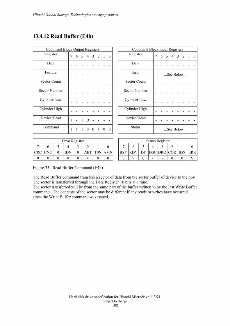
13.4.12 Read Buffer (E4h)
...See Below...Status00100111Command
--------Device/Head----D1-1Device/Head
--------Cylinder High--------Cylinder High
--------Cylinder Low--------Cylinder Low
--------Sector Number--------Sector Number
--------Sector Count--------Sector Count
...See Below...Error--------Feature
--------Data--------Data
01234567Register01234567RegisterCommand Block Input RegistersCommand Block Output Registers
V00--0V000V00000ERRIDXCORDRQDSCDFRDYBSYAMNT0NABT0IDN0UNCCRC
0123456701234567Status RegisterError Register
Figure 35. Read Buffer Command (E4h)
The Read Buffer command transfers a sector of data from the sector buffer of device to the host.The sector is transferred through the Data Register 16 bits at a time.The sector transferred will be from the same part of the buffer written to by the last Write Buffercommand. The contents of the sector may be different if any reads or writes have occurredsince the Write Buffer command was issued.
Hitachi Global Storage Technologies storage products
Hard disk drive specfication for Hitachi MicrodriveTM 3K4 Subject to change
108

13.4.13 Read DMA(C8h/C9h)
...See Below...StatusR0010011Command
HHHH----Device/HeadHHHHD1L1Device/Head
VVVVVVVVCylinder HighVVVVVVVVCylinder High
VVVVVVVVCylinder LowVVVVVVVVCylinder Low
VVVVVVVVSector NumberVVVVVVVVSector Number
VVVVVVVVSector CountVVVVVVVVSector Count
...See Below...Error--------Feature
--------Data--------Data
01234567Register01234567RegisterCommand Block Input RegistersCommand Block Output Registers
V00-V0V0V0V0V0VVERRIDXCORDRQDSCDFRDYBSYAMNT0NABT0IDN0UNCCRC
0123456701234567Status RegisterError Register
Figure 36. Read DMA Command (C8h/C9h)
The Read DMA command reads one or more sectors of data from disk media, then transfers thedata from the device to the host.The sectors are transferred through the Data Register 16 bits at a time.The host initializes a slave-DMA channel prior to issuing the command. The data transfers arequalified by DMARQ and are performed by the slave-DMA channel. The device issues onlyone interrupt per command to indicate that data transfer has terminated and status is available.If an uncorrectable error occurs, the read will be terminated at the failing sector.
The number of requested sectors not transferred. This will be zero, unlessSector CountInput Parameters From The Device
The retry bit. If set to one, then retries are disabled.R
The head number of the first sector to be transferred. (L=0)In LBA mode, this register specifies LBA bits 24-27 to be transferred.(L=1)
H
The cylinder number of the first sector to be transferred. (L=0)In LBA mode, this register specifies LBA address bits 8 - 15 (Low) 16 - 23(High) to be transferred. (L=1)
Cylinder High/Low
The sector number of the first sector to be transferred. (L=0)In LBA mode, this register specifies LBA address bits 0 - 7 to betransferred. (L=1)
Sector Number
The number of continuous sectors to be transferred. If zero is specified,then 256 sectors will be transferred.
Sector CountOutput Parameters To The Device
Hitachi Global Storage Technologies storage products
Hard disk drive specfication for Hitachi MicrodriveTM 3K4 Subject to change
109
The head number of the sector to be transferred. (L=0)In LBA mode, this register contains current LBA bits 24 - 27. (L=1)
H
The cylinder number of the last transferred sector. (L=0)In LBA mode, this register contains current LBA bits 8 - 15 (Low), 16 - 23(High). (L=1)
Cylinder High/Low
The sector number of the last transferred sector. (L=0)In LBA mode, this register contains current LBA bits 0 - 7. (L=1)
Sector Number
an unrecoverable error occurs.
Hitachi Global Storage Technologies storage products
Hard disk drive specfication for Hitachi MicrodriveTM 3K4 Subject to change
110
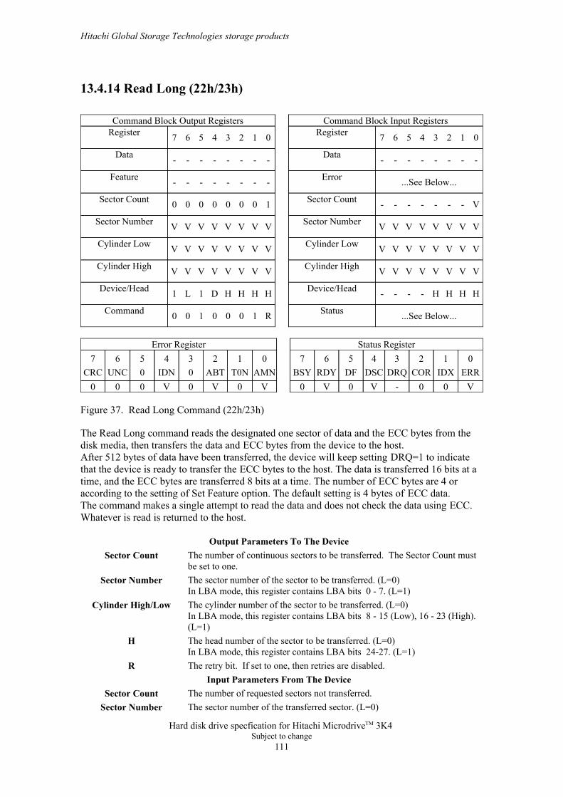
13.4.14 Read Long (22h/23h)
...See Below...StatusR1000100Command
HHHH----Device/HeadHHHHD1L1Device/Head
VVVVVVVVCylinder HighVVVVVVVVCylinder High
VVVVVVVVCylinder LowVVVVVVVVCylinder Low
VVVVVVVVSector NumberVVVVVVVVSector Number
V-------Sector Count10000000Sector Count
...See Below...Error--------Feature
--------Data--------Data
01234567Register01234567RegisterCommand Block Input RegistersCommand Block Output Registers
V00-V0V0V0V0V000ERRIDXCORDRQDSCDFRDYBSYAMNT0NABT0IDN0UNCCRC
0123456701234567Status RegisterError Register
Figure 37. Read Long Command (22h/23h)
The Read Long command reads the designated one sector of data and the ECC bytes from thedisk media, then transfers the data and ECC bytes from the device to the host.After 512 bytes of data have been transferred, the device will keep setting DRQ=1 to indicatethat the device is ready to transfer the ECC bytes to the host. The data is transferred 16 bits at atime, and the ECC bytes are transferred 8 bits at a time. The number of ECC bytes are 4 or according to the setting of Set Feature option. The default setting is 4 bytes of ECC data.The command makes a single attempt to read the data and does not check the data using ECC.Whatever is read is returned to the host.
The sector number of the transferred sector. (L=0)Sector NumberThe number of requested sectors not transferred.Sector Count
Input Parameters From The DeviceThe retry bit. If set to one, then retries are disabled.R
The head number of the sector to be transferred. (L=0)In LBA mode, this register contains LBA bits 24-27. (L=1)
H
The cylinder number of the sector to be transferred. (L=0)In LBA mode, this register contains LBA bits 8 - 15 (Low), 16 - 23 (High).(L=1)
Cylinder High/Low
The sector number of the sector to be transferred. (L=0)In LBA mode, this register contains LBA bits 0 - 7. (L=1)
Sector Number
The number of continuous sectors to be transferred. The Sector Count mustbe set to one.
Sector CountOutput Parameters To The Device
Hitachi Global Storage Technologies storage products
Hard disk drive specfication for Hitachi MicrodriveTM 3K4 Subject to change
111
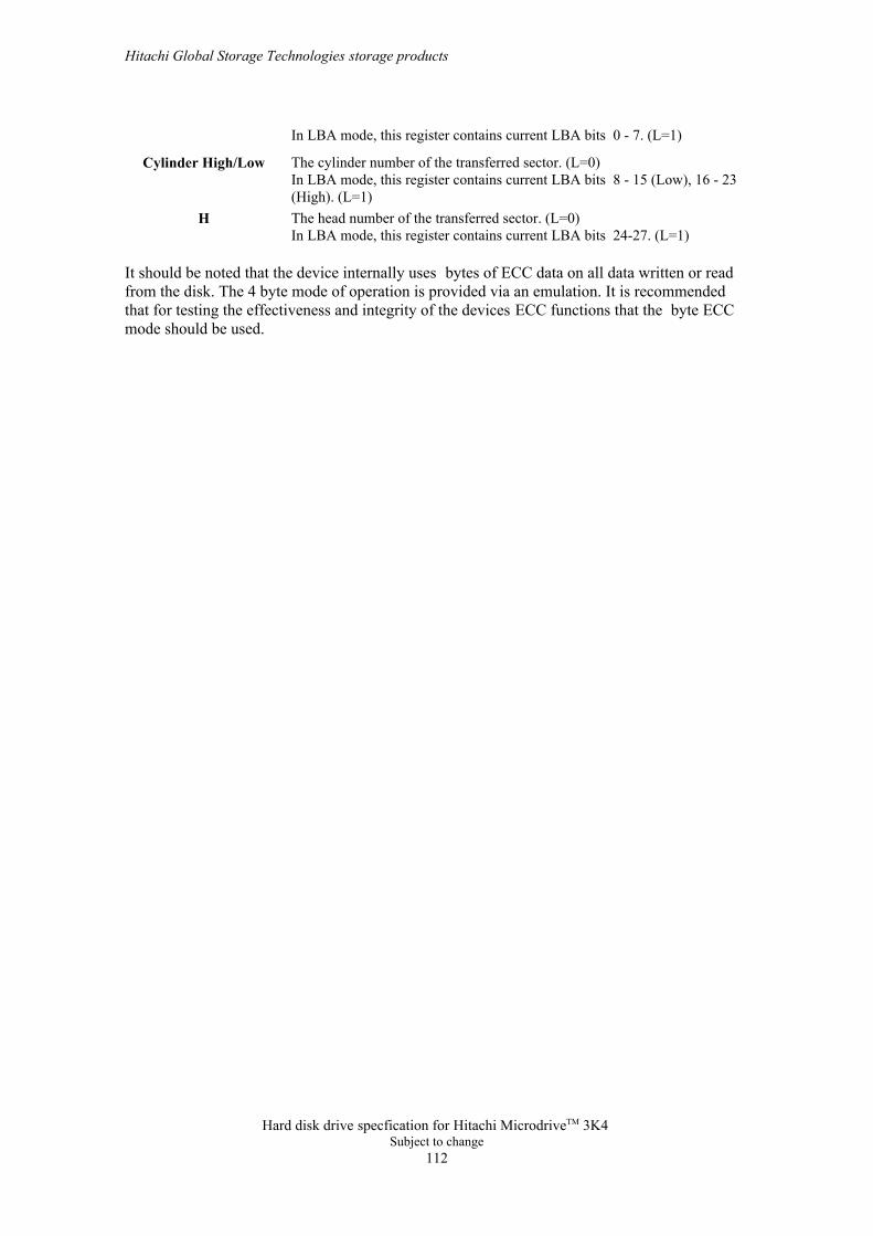
The head number of the transferred sector. (L=0)In LBA mode, this register contains current LBA bits 24-27. (L=1)
H
The cylinder number of the transferred sector. (L=0)In LBA mode, this register contains current LBA bits 8 - 15 (Low), 16 - 23(High). (L=1)
Cylinder High/Low
In LBA mode, this register contains current LBA bits 0 - 7. (L=1)
It should be noted that the device internally uses bytes of ECC data on all data written or readfrom the disk. The 4 byte mode of operation is provided via an emulation. It is recommendedthat for testing the effectiveness and integrity of the devices ECC functions that the byte ECCmode should be used.
Hitachi Global Storage Technologies storage products
Hard disk drive specfication for Hitachi MicrodriveTM 3K4 Subject to change
112

13.4.15 Read Multiple (C4h)
...See Below...Status00100011Command
HHHH----Device/HeadHHHHD1L1Device/Head
VVVVVVVVCylinder HighVVVVVVVVCylinder High
VVVVVVVVCylinder LowVVVVVVVVCylinder Low
VVVVVVVVSector NumberVVVVVVVVSector Number
VVVVVVVVSector CountVVVVVVVVSector Count
...See Below...Error--------Feature
--------Data--------Data
01234567Register01234567RegisterCommand Block Input RegistersCommand Block Output Registers
V00-V0V0V0V0V0V0ERRIDXCORDRQDSCDFRDYBSYAMNT0NABT0IDN0UNCCRC
0123456701234567Status RegisterError Register
Figure 38. Read Multiple Command (C4h)
The Read Multiple command reads one or more sectors of data from disk media, then transfersthe data from the device to the host.The sectors are transferred through the Data Register 16 bits at a time. Command execution isidentical to the Read Sectors command except that an interrupt is generated for each block (asdefined by the Set Multiple command) instead of for each sector.
The cylinder number of the last transferred sector. (L=0)Cylinder High/Low
The sector number of the last transferred sector. (L=0)In LBA mode, this register contains current LBA bits 0 - 7. (L=1)
Sector Number
The number of requested sectors not transferred. This will be zero, unlessan unrecoverable error occurs.
Sector CountInput Parameters From The Device
The head number of the first sector to be transferred. (L=0)In LBA mode, this register contains LBA bits 24 - 27. (L=1)
H
The cylinder number of the first sector to be transferred. (L=0)In LBA mode, this register contains LBA bits 8 - 15 (Low), 16 - 23 (High).(L=1)
Cylinder High/Low
The sector number of the first sector to be transferred. (L=0)In LBA mode, this register contains LBA bits 0 - 7. (L=1)
Sector Number
The number of continuous sectors to be transferred. If zero is specified,then 256 sectors will be transferred.
Sector CountOutput Parameters To The Device
Hitachi Global Storage Technologies storage products
Hard disk drive specfication for Hitachi MicrodriveTM 3K4 Subject to change
113
The head number of the last transferred sector. (L=0)LBA mode, this register contains current LBA bits 24 - 27. (L=1)
H
In LBA mode, this register contains current LBA bits 8-15 (Low), 16-23(High). (L=1)
Hitachi Global Storage Technologies storage products
Hard disk drive specfication for Hitachi MicrodriveTM 3K4 Subject to change
114
13.4.16 Read Sector(s) (20h/21h)
...See Below...StatusR0000100Command
HHHH----Device/HeadHHHHD1L1Device/Head
VVVVVVVVCylinder HighVVVVVVVVCylinder High
VVVVVVVVCylinder LowVVVVVVVVCylinder Low
VVVVVVVVSector NumberVVVVVVVVSector Number
VVVVVVVVSector CountVVVVVVVVSector Count
...See Below...Error--------Feature
--------Data--------Data
01234567Register01234567RegisterCommand Block Input RegistersCommand Block Output Registers
V00-V0V0V0V0V0V0ERRIDXCORDRQDSCDFRDYBSYAMNT0NABT0IDN0UNCCRC
0123456701234567Status RegisterError Register
Figure 39. Read Sector(s) Command (20h/21h)
The Read Sectors command reads one or more sectors of data from disk media, then transfersthe data from the device to the host.The sectors are transferred through the Data Register 16 bits at a time.If an uncorrectable error occurs, the read will be terminated at the failing sector.
The cylinder number of the last transferred sector. (L=0)Cylinder High/Low
The sector number of the last transferred sector. (L=0)In LBA mode, this register contains current LBA bits 0 - 7. (L=1)
Sector Number
The number of requested sectors not transferred. This will be zero, unlessan unrecoverable error occurs.
Sector CountInput Parameters From The Device
The retry bit. If set to one, then retries are disabled.R
The head number of the first sector to be transferred. (L=0)In LBA mode, this register contains LBA bits 24 - 27. (L=1)
H
The cylinder number of the first sector to be transferred. (L=0)In LBA mode, this register contains LBA bits 8 - 15 (Low), 16 - 23 (High).(L=1)
Cylinder High/Low
The sector number of the first sector to be transferred. (L=0)In LBA mode, this register contains LBA bits 0 - 7. (L=1)
Sector Number
The number of continuous sectors to be transferred. If zero is specified,then 256 sectors will be transferred.
Sector CountOutput Parameters To The Device
Hitachi Global Storage Technologies storage products
Hard disk drive specfication for Hitachi MicrodriveTM 3K4 Subject to change
115

The head number of the last transferred sector. (L=0)In LBA mode, this register contains current LBA bits 24 - 27. (L=1)
H
In LBA mode, this register contains current LBA bits 8 - 15 (Low), 16 - 23(High). (L=1)
Hitachi Global Storage Technologies storage products
Hard disk drive specfication for Hitachi MicrodriveTM 3K4 Subject to change
116
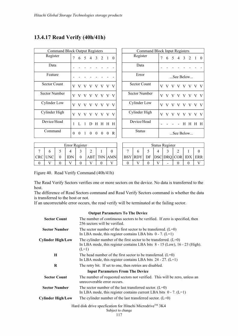
13.4.17 Read Verify (40h/41h)
...See Below...StatusR0000100Command
HHHH----Device/HeadHHHHD1L1Device/Head
VVVVVVVVCylinder HighVVVVVVVVCylinder High
VVVVVVVVCylinder LowVVVVVVVVCylinder Low
VVVVVVVVSector NumberVVVVVVVVSector Number
VVVVVVVVSector CountVVVVVVVVSector Count
...See Below...Error--------Feature
--------Data--------Data
01234567Register01234567RegisterCommand Block Input RegistersCommand Block Output Registers
V00-V0V0V0V0V0V0ERRIDXCORDRQDSCDFRDYBSYAMNT0NABT0IDN0UNCCRC
0123456701234567Status RegisterError Register
Figure 40. Read Verify Command (40h/41h)
The Read Verify Sectors verifies one or more sectors on the device. No data is transferred to thehost.The difference of Read Sectors command and Read Verify Sectors command is whether the datais transferred to the host or not.If an uncorrectable error occurs, the read verify will be terminated at the failing sector.
The cylinder number of the last transferred sector. (L=0)Cylinder High/Low
The sector number of the last transferred sector. (L=0)In LBA mode, this register contains current LBA bits 0 - 7. (L=1)
Sector Number
The number of requested sectors not verified. This will be zero, unless anunrecoverable error occurs.
Sector CountInput Parameters From The Device
The retry bit. If set to one, then retries are disabled.R
The head number of the first sector to be transferred. (L=0)In LBA mode, this register contains LBA bits 24 - 27. (L=1)
H
The cylinder number of the first sector to be transferred. (L=0)In LBA mode, this register contains LBA bits 8 - 15 (Low), 16 - 23 (High).(L=1)
Cylinder High/Low
The sector number of the first sector to be transferred. (L=0)In LBA mode, this register contains LBA bits 0 - 7. (L=1)
Sector Number
The number of continuous sectors to be verified. If zero is specified, then256 sectors will be verified.
Sector CountOutput Parameters To The Device
Hitachi Global Storage Technologies storage products
Hard disk drive specfication for Hitachi MicrodriveTM 3K4 Subject to change
117
The head number of the last transferred sector. (L=0)In LBA mode, this register contains current LBA bits 24 - 27. (L=1)
H
In LBA mode, this register contains current LBA bits 8 - 15 (Low), 16 - 23(High). (L=1)
Hitachi Global Storage Technologies storage products
Hard disk drive specfication for Hitachi MicrodriveTM 3K4 Subject to change
118
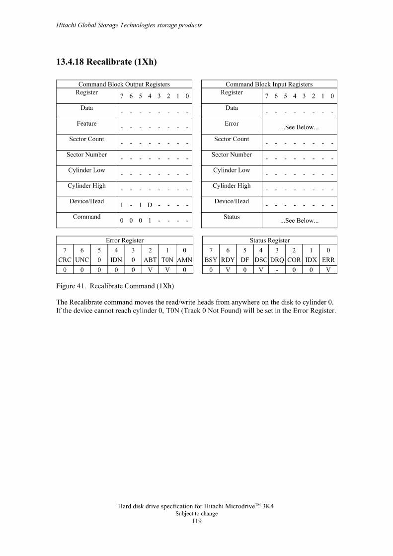
13.4.18 Recalibrate (1Xh)
...See Below...Status----1000Command
--------Device/Head----D1-1Device/Head
--------Cylinder High--------Cylinder High
--------Cylinder Low--------Cylinder Low
--------Sector Number--------Sector Number
--------Sector Count--------Sector Count
...See Below...Error--------Feature
--------Data--------Data
01234567Register01234567RegisterCommand Block Input RegistersCommand Block Output Registers
V00-V0V00VV00000ERRIDXCORDRQDSCDFRDYBSYAMNT0NABT0IDN0UNCCRC
0123456701234567Status RegisterError Register
Figure 41. Recalibrate Command (1Xh)
The Recalibrate command moves the read/write heads from anywhere on the disk to cylinder 0.If the device cannot reach cylinder 0, T0N (Track 0 Not Found) will be set in the Error Register.
Hitachi Global Storage Technologies storage products
Hard disk drive specfication for Hitachi MicrodriveTM 3K4 Subject to change
119
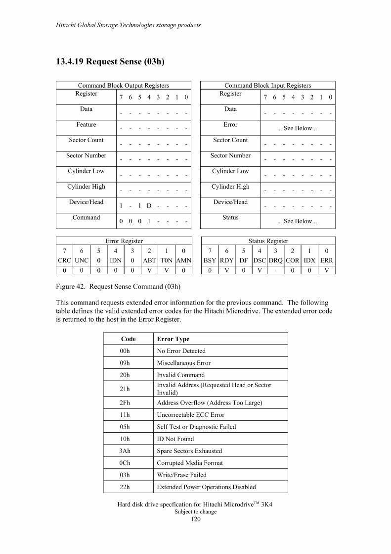
13.4.19 Request Sense (03h)
...See Below...Status----1000Command
--------Device/Head----D1-1Device/Head
--------Cylinder High--------Cylinder High
--------Cylinder Low--------Cylinder Low
--------Sector Number--------Sector Number
--------Sector Count--------Sector Count
...See Below...Error--------Feature
--------Data--------Data
01234567Register01234567RegisterCommand Block Input RegistersCommand Block Output Registers
V00-V0V00VV00000ERRIDXCORDRQDSCDFRDYBSYAMNT0NABT0IDN0UNCCRC
0123456701234567Status RegisterError Register
Figure 42. Request Sense Command (03h)
This command requests extended error information for the previous command. The followingtable defines the valid extended error codes for the Hitachi Microdrive. The extended error codeis returned to the host in the Error Register.
Extended Power Operations Disabled22h
Write/Erase Failed03h
Corrupted Media Format0Ch
Spare Sectors Exhausted3Ah
ID Not Found10h
Self Test or Diagnostic Failed05h
Uncorrectable ECC Error11h
Address Overflow (Address Too Large)2Fh
Invalid Address (Requested Head or SectorInvalid)21h
Invalid Command20h
Miscellaneous Error09h
No Error Detected00h
Error TypeCode
Hitachi Global Storage Technologies storage products
Hard disk drive specfication for Hitachi MicrodriveTM 3K4 Subject to change
120
Figure 43. Extended Error Codes
Hitachi Global Storage Technologies storage products
Hard disk drive specfication for Hitachi MicrodriveTM 3K4 Subject to change
121
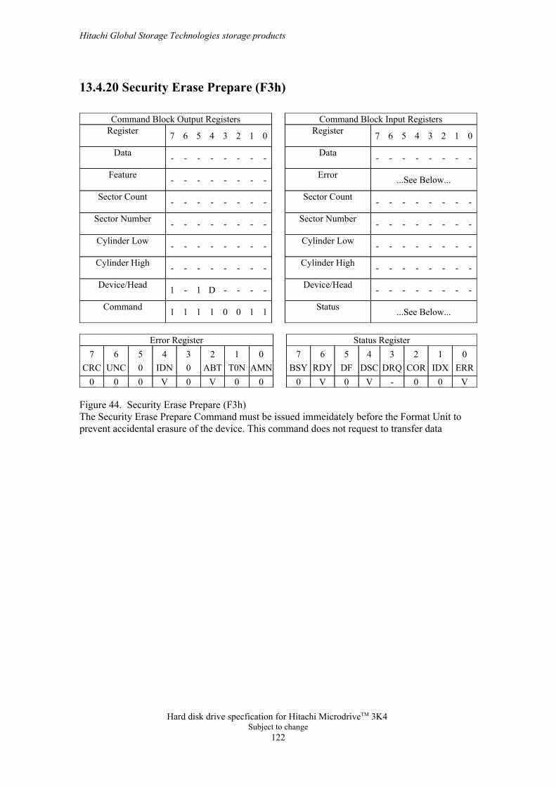
13.4.20 Security Erase Prepare (F3h)
...See Below...Status11001111Command
--------Device/Head----D1-1Device/Head
--------Cylinder High--------Cylinder High
--------Cylinder Low--------Cylinder Low
--------Sector Number--------Sector Number
--------Sector Count--------Sector Count
...See Below...Error--------Feature
--------Data--------Data
01234567Register01234567RegisterCommand Block Input RegistersCommand Block Output Registers
V00-V0V000V0V000ERRIDXCORDRQDSCDFRDYBSYAMNT0NABT0IDN0UNCCRC
0123456701234567Status RegisterError Register
Figure 44. Security Erase Prepare (F3h) The Security Erase Prepare Command must be issued immeidately before the Format Unit toprevent accidental erasure of the device. This command does not request to transfer data
Hitachi Global Storage Technologies storage products
Hard disk drive specfication for Hitachi MicrodriveTM 3K4 Subject to change
122
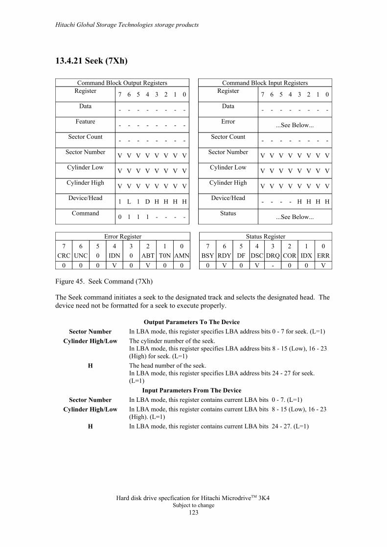
13.4.21 Seek (7Xh)
...See Below...Status----1110Command
HHHH----Device/HeadHHHHD1L1Device/Head
VVVVVVVVCylinder HighVVVVVVVVCylinder High
VVVVVVVVCylinder LowVVVVVVVVCylinder Low
VVVVVVVVSector NumberVVVVVVVVSector Number
--------Sector Count--------Sector Count
...See Below...Error--------Feature
--------Data--------Data
01234567Register01234567RegisterCommand Block Input RegistersCommand Block Output Registers
V00-V0V000V0V000ERRIDXCORDRQDSCDFRDYBSYAMNT0NABT0IDN0UNCCRC
0123456701234567Status RegisterError Register
Figure 45. Seek Command (7Xh)
The Seek command initiates a seek to the designated track and selects the designated head. Thedevice need not be formatted for a seek to execute properly.
In LBA mode, this register contains current LBA bits 24 - 27. (L=1)H
In LBA mode, this register contains current LBA bits 8 - 15 (Low), 16 - 23(High). (L=1)
Cylinder High/LowIn LBA mode, this register contains current LBA bits 0 - 7. (L=1)Sector Number
Input Parameters From The Device
The head number of the seek.In LBA mode, this register specifies LBA address bits 24 - 27 for seek.(L=1)
H
The cylinder number of the seek.In LBA mode, this register specifies LBA address bits 8 - 15 (Low), 16 - 23(High) for seek. (L=1)
Cylinder High/LowIn LBA mode, this register specifies LBA address bits 0 - 7 for seek. (L=1)Sector Number
Output Parameters To The Device
Hitachi Global Storage Technologies storage products
Hard disk drive specfication for Hitachi MicrodriveTM 3K4 Subject to change
123
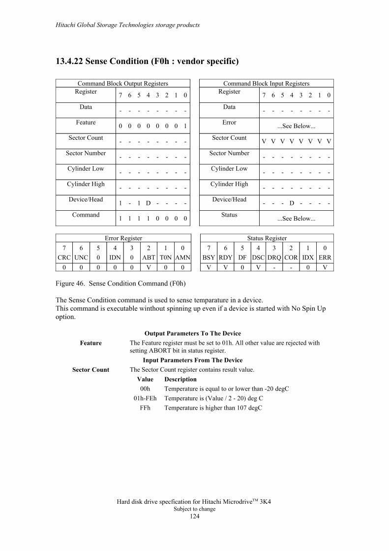
13.4.22 Sense Condition (F0h : vendor specific)
...See Below...Status00001111Command
----D---Device/Head----D1-1Device/Head
--------Cylinder High--------Cylinder High
--------Cylinder Low--------Cylinder Low
--------Sector Number--------Sector Number
VVVVVVVVSector Count--------Sector Count
...See Below...Error10000000Feature
--------Data--------Data
01234567Register01234567RegisterCommand Block Input RegistersCommand Block Output Registers
V0--V0VV00V00000ERRIDXCORDRQDSCDFRDYBSYAMNT0NABT0IDN0UNCCRC
0123456701234567Status RegisterError Register
Figure 46. Sense Condition Command (F0h)
The Sense Condition command is used to sense temparature in a device.This command is executable winthout spinning up even if a device is started with No Spin Upoption.
Temperature is higher than 107 degCFFhTemperature is (Value / 2 - 20) deg C01h-FEhTemperature is equal to or lower than -20 degC00hDescriptionValue
The Sector Count register contains result value.Sector CountInput Parameters From The Device
The Feature register must be set to 01h. All other value are rejected withsetting ABORT bit in status register.
FeatureOutput Parameters To The Device
Hitachi Global Storage Technologies storage products
Hard disk drive specfication for Hitachi MicrodriveTM 3K4 Subject to change
124
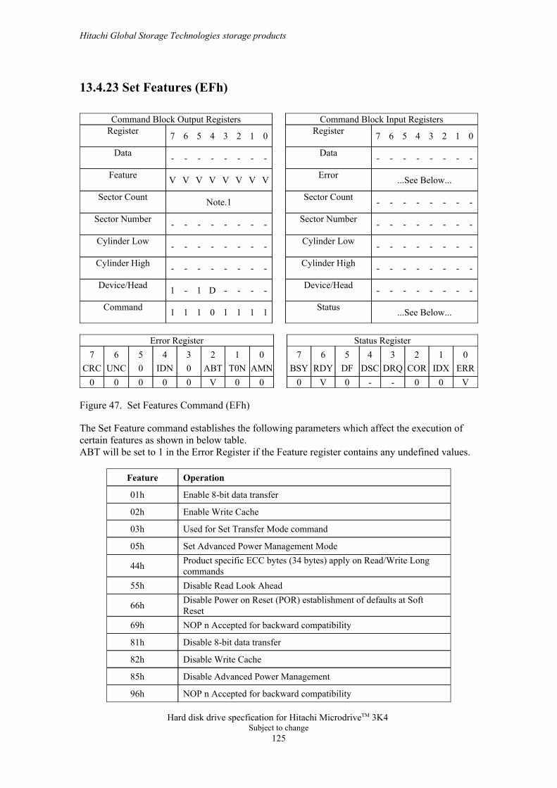
13.4.23 Set Features (EFh)
...See Below...Status11110111Command
--------Device/Head----D1-1Device/Head
--------Cylinder High--------Cylinder High
--------Cylinder Low--------Cylinder Low
--------Sector Number--------Sector Number
--------Sector CountNote.1Sector Count
...See Below...ErrorVVVVVVVVFeature
--------Data--------Data
01234567Register01234567RegisterCommand Block Input RegistersCommand Block Output Registers
V00--0V000V00000ERRIDXCORDRQDSCDFRDYBSYAMNT0NABT0IDN0UNCCRC
0123456701234567Status RegisterError Register
Figure 47. Set Features Command (EFh)
The Set Feature command establishes the following parameters which affect the execution ofcertain features as shown in below table.ABT will be set to 1 in the Error Register if the Feature register contains any undefined values.
NOP n Accepted for backward compatibility96h
Disable Advanced Power Management85h
Disable Write Cache82h
Disable 8-bit data transfer81h
NOP n Accepted for backward compatibility69h
Disable Power on Reset (POR) establishment of defaults at SoftReset66h
Disable Read Look Ahead55h
Product specific ECC bytes (34 bytes) apply on Read/Write Longcommands44h
Set Advanced Power Management Mode05h
Used for Set Transfer Mode command03h
Enable Write Cache02h
Enable 8-bit data transfer01h
OperationFeature
Hitachi Global Storage Technologies storage products
Hard disk drive specfication for Hitachi MicrodriveTM 3K4 Subject to change
125
Enable Power on Rest (POR) establishment of defaults at Soft ResetCCh
4 bytes of ECC apply on Read/Write Long commandsBBh
Enable Read Look AheadAAh
NOP n Accepted for backward compatibility9Ah
Accepted for backward compatibility. Use of this feature is notrecommended97h
Figure 48. Features Supported
Features 01h and 81h are used to enable and clear 8 bit data transfer modes in True IDE Mode.If the 01h feature command is issued all data transfers will occur on the low order D7-D0 databus and the IOIS16 signal will not be asserted for data register accesses.Features 82h, AAh and BBh are the default features for the Hitachi Microdrive, thus, the hostdoes not have to issue this command with these features unless it is necessary for compatibilityreasons.Features 66h and CCh can be used to enable and disable whether the Power On Reset (POR)Defaults will be set when a soft reset occurs. The default setting is to revert to the POR defaultswhen a soft reset occurs.Feature 05h is used for advanced power management. The Sector Count Register specifies theadvanced power management level as below. The advanced power management level at poweron resetis 60h.
80h - FEh Up to Low Power Idle mode01h - 7Fh Up to Standby mode00h, FFh Reserved
Feature 85h is used to disable advanced power management. This results in the same effect asthe host uses features 05h with the Sector Count Register FEh.
Hitachi Global Storage Technologies storage products
Hard disk drive specfication for Hitachi MicrodriveTM 3K4 Subject to change
126
13.4.24 Set Multiple (C6h)
...See Below...Status01100011Command
--------Device/Head----D1-1Device/Head
--------Cylinder High--------Cylinder High
--------Cylinder Low--------Cylinder Low
--------Sector Number--------Sector Number
--------Sector CountVVVVVVVVSector Count
...See Below...Error--------Feature
--------Data--------Data
01234567Register01234567RegisterCommand Block Input RegistersCommand Block Output Registers
V00--0V000V00000ERRIDXCORDRQDSCDFRDYBSYAMNT0NABT0IDN0UNCCRC
0123456701234567Status RegisterError Register
Figure 49. Set Multiple Command (C6h)
The Set Multiple command enables the device to perform Read and Write Multiple commandsand establishes the block size for these commands. The block size is the number of sectors to betransferred for each interrupt.The default block size after power up, or hard reset is 0, and Read Multiple and Write Multiplecommands are disabled.If an invalid block size is specified, an Abort error will be returned to the host, and ReadMultiple and Write Multiple commands will be disabled.
The block size to be used for Read Multiple and Write Multiple commands.Valid block sizes can be selected from 0, 1, 2, 4, 8 or 16. If 0 is specified,then Read Multiple and Write Multiple commands are disabled.
Sector CountOutput Parameters To The Device
Hitachi Global Storage Technologies storage products
Hard disk drive specfication for Hitachi MicrodriveTM 3K4 Subject to change
127
13.4.25 Sleep (E6h/99h)
...See Below...Status01100111Command
--------Device/Head----D1-1Device/Head
--------Cylinder High--------Cylinder High
--------Cylinder Low--------Cylinder Low
--------Sector Number--------Sector Number
--------Sector Count--------Sector Count
...See Below...Error--------Feature
--------Data--------Data
01234567Register01234567RegisterCommand Block Input RegistersCommand Block Output Registers
V00-V0V000V00000ERRIDXCORDRQDSCDFRDYBSYAMNT0NABT0IDN0UNCCRC
0123456701234567Status RegisterError Register
Figure 50. Sleep Command (E6h/99h)
The Sleep command causes the device to enter the Sleep Mode immediately. When this command is issued, the device confirms the completion of the cached writecommands before it asserts INTRQ. Then the device is spun down. If the device is already spundown, the spin down sequence is not executed. It is not required to use a software reset or ahardware reset to recover from Sleep Mode, but simply issue a command to the device.
Hitachi Global Storage Technologies storage products
Hard disk drive specfication for Hitachi MicrodriveTM 3K4 Subject to change
128
13.4.26Standby (E2h/96h)
...See Below...Status01000111Command
--------Device/Head----D1-1Device/Head
--------Cylinder High--------Cylinder High
--------Cylinder Low--------Cylinder Low
--------Sector Number--------Sector Number
--------Sector CountVVVVVVVVSector Count
...See Below...Error--------Feature
--------Data--------Data
01234567Register01234567RegisterCommand Block Input RegistersCommand Block Output Registers
V00-V0V000V00000ERRIDXCORDRQDSCDFRDYBSYAMNT0NABT0IDN0UNCCRC
0123456701234567Status RegisterError Register
Figure 51. Standby Command (E2h/96h)
The Standby command causes the device to enter the Standby Mode immediately, and set autopower down timeout parameter(standby timer). When this command is issued, the device confirms the completion of the cached writecommands before it asserts INTRQ. Then the device is spun down, but the interface remainsactive.If the device is already spun down, the spin down sequence is not executed.During the Standby mode the device will respond to commands, but there is a delay whilewaiting for the spindle to reach operating speed.The timer starts counting down when the device returns to Idle mode.
Timeout Parameter. If zero, the timeout interval(Standby Timer) is NOTdisabled, but the timeout interval is set to 109 minutes automatically. Ifother than zero, the timeout interval is set for (Timeout Parameter x5)seconds. When the automatic power down sequence is enabled,The device will enter Standby mode automatically if the timeout intervalexpires with no device access from the host. The timeout interval will bereinitialized if there is a device access before the timeout interval expires.
Sector CountOutput Parameters To The Device
Hitachi Global Storage Technologies storage products
Hard disk drive specfication for Hitachi MicrodriveTM 3K4 Subject to change
129
13.4.27 Standby Immediate (E0h/94h)
...See Below...Status00000111Command
--------Device/Head----D1-1Device/Head
--------Cylinder High--------Cylinder High
--------Cylinder Low--------Cylinder Low
--------Sector Number--------Sector Number
--------Sector Count--------Sector Count
...See Below...Error--------Feature
--------Data--------Data
01234567Register01234567RegisterCommand Block Input RegistersCommand Block Output Registers
V00-V0V000V00000ERRIDXCORDRQDSCDFRDYBSYAMNT0NABT0IDN0UNCCRC
0123456701234567Status RegisterError Register
Figure 52. Standby Immediate Command (E0h/94h)
The Standby Immediate command causes the device to enter Standby mode immediately.When this command is issued, the device confirms the completion of the cached writecommands before asserts INTRQ. Then the device is spun down, but the interface remainsactive.If the device is already spun down, the spin down sequence is not executed.During the Standby mode, the device will respond to commands, but there is a delay whilewaiting for the spindle to reach operating speed.The Standby Immediate command will not affect the auto power down timeout parameter.
Hitachi Global Storage Technologies storage products
Hard disk drive specfication for Hitachi MicrodriveTM 3K4 Subject to change
130
13.4.28 Translate Sector (87h)
...See Below...StatusR0000100Command
HHHH----Device/HeadHHHHD1L1Device/Head
VVVVVVVVCylinder HighVVVVVVVVCylinder High
VVVVVVVVCylinder LowVVVVVVVVCylinder Low
VVVVVVVVSector NumberVVVVVVVVSector Number
--------Sector Count--------Sector Count
...See Below...Error--------Feature
--------Data--------Data
01234567Register01234567RegisterCommand Block Input RegistersCommand Block Output Registers
V00-V0V0V0V0V0V0ERRIDXCORDRQDSCDFRDYBSYAMNT0NABT0IDN0UNCCRC
0123456701234567Status RegisterError Register
Figure 53. Translate Sector command (87h)
This command allows the host a method of determining the exact number of times a user sectorhas been erased and programmed. The controller responds with a 512 byte buffer of informationcontaining the desired cylinder, head and sector, including its Logical Address, and the HotCount, if available, for that sector. The following table represents the information in the buffer.Please note that this command is unique to the card.
Reserved1Bh-1FFh
Hot Count MSB (18) - LSB (1A)18h-1Ah
Reserved14h-17h
Erased Flag (FFh) = Erased; 00h = Not Erased13h
Reserved07h-12h
LBA MSB (04) - LSB (06)04h-06h
Sector03h
Head02h
Cylinder MSB (00), Cylinder LSB (01)00h-01h
InformationAddress
Figure 54. Translate Sector Information
Hitachi Global Storage Technologies storage products
Hard disk drive specfication for Hitachi MicrodriveTM 3K4 Subject to change
131
13.4.29 Wear Level (F5h)
...See Below...Status10101111Command
--------Device/HeadVVVVD1-1Device/Head
--------Cylinder High--------Cylinder High
--------Cylinder Low--------Cylinder Low
--------Sector Number--------Sector Number
00000000Sector Count--------Sector Count
...See Below...Error--------Feature
--------Data--------Data
01234567Register01234567RegisterCommand Block Input RegistersCommand Block Output Registers
V00-V0V000V00000ERRIDXCORDRQDSCDFRDYBSYAMNT0NABT0IDN0UNCCRC
0123456701234567Status RegisterError Register
Figure 55. Wear Level Command (F5h)
This command is implemented as a nop command. However, the Sector Count Register isreturned with 00h for backward compatibility.
Hitachi Global Storage Technologies storage products
Hard disk drive specfication for Hitachi MicrodriveTM 3K4 Subject to change
132
13.4.30 Write Buffer (E8h)
...See Below...Status00010111Command
--------Device/Head----D1-1Device/Head
--------Cylinder High--------Cylinder High
--------Cylinder Low--------Cylinder Low
--------Sector Number--------Sector Number
--------Sector Count--------Sector Count
...See Below...Error--------Feature
--------Data--------Data
01234567Register01234567RegisterCommand Block Input RegistersCommand Block Output Registers
V00--0V000V00000ERRIDXCORDRQDSCDFRDYBSYAMNT0NABT0IDN0UNCCRC
0123456701234567Status RegisterError Register
Figure 56. Write Buffer Command (E8h)
The Write Buffer command transfers a sector of data from the host to the sector buffer of thedevice. The sectors of data are transferred through the Data Register 16 bits at a time. The Read Buffer and Write Buffer commands are synchronized such that sequential WriteBuffer and Read Buffer commands access the same 512 byte within the buffer.
Hitachi Global Storage Technologies storage products
Hard disk drive specfication for Hitachi MicrodriveTM 3K4 Subject to change
133
13.4.31 Write DMA (CAh/CBh)
...See Below...StatusR1010011Command
HHHH----Device/HeadHHHHD1L1Device/Head
VVVVVVVVCylinder HighVVVVVVVVCylinder High
VVVVVVVVCylinder LowVVVVVVVVCylinder Low
VVVVVVVVSector NumberVVVVVVVVSector Number
VVVVVVVVSector CountVVVVVVVVSector Count
...See Below...Error--------Feature
--------Data--------Data
01234567Register01234567RegisterCommand Block Input RegistersCommand Block Output Registers
V00-VVV000V0V00VERRIDXCORDRQDSCDFRDYBSYAMNT0NABT0IDN0UNCCRC
0123456701234567Status RegisterError Register
Figure 57. Write DMA Command (CAh/CBh)
The Write DMA command transfers one or more sectors of data from the host to the device,then the data is written to the disk media.The sectors of data are transferred through the Data Register 16 bits at a time.The host initializes a slave-DMA channel prior to issuing the command. Data transfers arequalified by DMARQ and are performed by the slave-DMA channel. The device issues onlyone interrupt per command to indicate that data transfer has terminated and status is available.If an uncorrectable error occurs, the write will be terminated at the failing sector.
Input Parameters From The Device
The retry bit. If set to one, then retries are disabled. When write cache isenabled, They are ignored. (Ignoring the retry bit is in violation of ATA-3.)
R
The head number of the first sector to be transferred. (L=0)In LBA mode, this register contains LBA bits 24 - 27. (L=1)
H
The cylinder number of the first sector to be transferred. (L=0)In LBA mode, this register contains LBA bits 8 - 15 (Low), 16 - 23 (High).(L=1)
Cylinder High/Low
The sector number of the first sector to be transferred. (L=0)In LBA mode, this register contains LBA bits 0 - 7. (L=1)
Sector Number
The number of continuous sectors to be transferred. If zero is specified,then 256 sectors will be transferred.
Sector Count
Output Parameters To The Device
Hitachi Global Storage Technologies storage products
Hard disk drive specfication for Hitachi MicrodriveTM 3K4 Subject to change
134
The head number of the last transferred sector. (L=0) In LBA mode, thisregister contains current LBA bits 24 - 27. (L=1)
H
The cylinder number of the last transferred sector. (L=0)In LBA mode, this register contains current LBA bits 8 - 15 (Low), 16 - 23(High). (L=1)
Cylinder High/Low
The sector number of the last transferred sector. (L=0)In LBA mode, this register contains current LBA bits 0 - 7. (L=1)
Sector Number
The number of requested sectors not transferred. This will be zero, unlessan unrecoverable error occurs.
Sector Count
Hitachi Global Storage Technologies storage products
Hard disk drive specfication for Hitachi MicrodriveTM 3K4 Subject to change
135
13.4.32 Write Long (32h/33h)
...See Below...StatusR1001100Command
HHHH----Device/HeadHHHHD1L1Device/Head
VVVVVVVVCylinder HighVVVVVVVVCylinder High
VVVVVVVVCylinder LowVVVVVVVVCylinder Low
VVVVVVVVSector NumberVVVVVVVVSector Number
V-------Sector Count10000000Sector Count
...See Below...Error--------Feature
--------Data--------Data
01234567Register01234567RegisterCommand Block Input RegistersCommand Block Output Registers
V00-VVV000V0V000ERRIDXCORDRQDSCDFRDYBSYAMNT0NABT0IDN0UNCCRC
0123456701234567Status RegisterError Register
Figure 58. Write Long Command (32h/33h)
The Write Long command transfers the data and the ECC bytes of the designated one sectorfrom the host to the device, then the data and the ECC bytes are written to the disk media.After 512 bytes of data have been transferred, the device will keep setting DRQ=1 to indicatethat the device is ready to receive the ECC bytes from the host. The data is transferred 16 bits ata time, and the ECC bytes are transferred 8 bits at a time. The number of ECC bytes are 4 or according to setting of Set Feature option. The default number after power on is 4 bytes.
The sector number of the sector to be transferred. (L=0) In LBA mode, thisregister contains current LBA bits 0 - 7. (L=1)
Sector Number
The number of requested sectors not transferred.Sector Count
Input Parameters From The Device
The retry bit. If set to one, then retries are disabled.R
The head number of the sector to be transferred. (L=0) In LBA mode, thisregister contains LBA bits 24 - 27. (L=1)
H
The cylinder number of the sector to be transferred. (L=0) In LBA mode,this register contains LBA bits 8 - 15 (Low), 16 - 23 (High). (L=1)
Cylinder High/Low
The sector number of the sector to be transferred. (L=0) In LBA mode, thisregister contains LBA bits 0 - 7. (L=1)
Sector Number
The number of continuous sectors to be transferred. The Sector Count mustbe set to one.
Sector Count
Output Parameters To The Device
Hitachi Global Storage Technologies storage products
Hard disk drive specfication for Hitachi MicrodriveTM 3K4 Subject to change
136
The head number of the sector to be transferred. (L=0) In LBA mode, thisregister contains current LBA bits 24 - 27. (L=1)
H
The cylinder number of the sector to be transferred. (L=0) In LBA mode,this register contains current LBA bits 8 - 15 (Low), 16 - 23 (High). (L=1)
Cylinder High/Low
The file internally uses bytes of ECC on all data read or writes. The 4 byte mode of operation isprovided via an emulation technique. As a consequence of this emulation it is recommendedthat byte ECC mode is used for all tests to confirm the operation of the files ECC hardware.Unexpected results may occur if such testing is performed using 4 byte mode.
Hitachi Global Storage Technologies storage products
Hard disk drive specfication for Hitachi MicrodriveTM 3K4 Subject to change
137
13.4.33 Write Multiple (C5h)
...See Below...Status10100011Command
HHHH----Device/HeadHHHHD1L1Device/Head
VVVVVVVVCylinder HighVVVVVVVVCylinder High
VVVVVVVVCylinder LowVVVVVVVVCylinder Low
VVVVVVVVSector NumberVVVVVVVVSector Number
VVVVVVVVSector CountVVVVVVVVSector Count
...See Below...Error--------Feature
--------Data--------Data
01234567Register01234567RegisterCommand Block Input RegistersCommand Block Output Registers
V00-VVV000V0V000ERRIDXCORDRQDSCDFRDYBSYAMNT0NABT0IDN0UNCCRC
0123456701234567Status RegisterError Register
Figure 59. Write Multiple Command (C5h)
The Write Multiple command transfers one or more sectors from the host to the device, then thedata is written to the disk media.Command execution is identical to the Write Sectors command except that an interrupt isgenerated for each block (as defined by the Set Multiple command) instead of for each sector.The sectors are transferred through the Data Register 16 bits at a time.
The cylinder number of the last transferred sector. (L=0)Cylinder High/Low
The sector number of the last transferred sector. (L=0)In LBA mode, this register contains current LBA bits 0 - 7. (L=1)
Sector Number
The number of requested sectors not transferred. This will be zero, unlessan unrecoverable error occurs.
Sector CountInput Parameters From The Device
The head number of the first sector to be transferred. (L=0)In LBA mode, this register contains LBA bits 24 - 27. (L=1)
H
The cylinder number of the first sector to be transferred. (L=0)In LBA mode, this register contains LBA bits 8 - 15 (Low), 16 - 23 (High).(L=1)
Cylinder High/Low
The sector number of the first sector to be transferred. (L=0)In LBA mode, this register contains LBA bits 0 - 7. (L=1)
Sector Number
The number of continuous sectors to be transferred. If zero is specified,then 256 sectors will be transferred.
Sector CountOutput Parameters To The Device
Hitachi Global Storage Technologies storage products
Hard disk drive specfication for Hitachi MicrodriveTM 3K4 Subject to change
138

The head number of the last transferred sector. (L=0)In LBA mode, this register contains current LBA bits 24 - 27. (L=1)
H
In LBA mode, this register contains current LBA bits 8 - 15 (Low), 16 - 23(High). (L=1)
Hitachi Global Storage Technologies storage products
Hard disk drive specfication for Hitachi MicrodriveTM 3K4 Subject to change
139

13.4.34 Write Multiple without Erase (CDh)
...See Below...StatusR0001100Command
HHHH----Device/HeadHHHHD1L1Device/Head
VVVVVVVVCylinder HighVVVVVVVVCylinder High
VVVVVVVVCylinder LowVVVVVVVVCylinder Low
VVVVVVVVSector NumberVVVVVVVVSector Number
VVVVVVVVSector CountVVVVVVVVSector Count
...See Below...Error--------Feature
--------Data--------Data
01234567Register01234567RegisterCommand Block Input RegistersCommand Block Output Registers
V00-VVV000V0V000ERRIDXCORDRQDSCDFRDYBSYAMNT0NABT0IDN0UNCCRC
0123456701234567Status RegisterError Register
Figure 60. Write Multiple without Erase Command (CDh)
This command is identical to the Write Multiple command as the Hitachi Microdrive does notneed pre-erase before a write operation.
Hitachi Global Storage Technologies storage products
Hard disk drive specfication for Hitachi MicrodriveTM 3K4 Subject to change
140
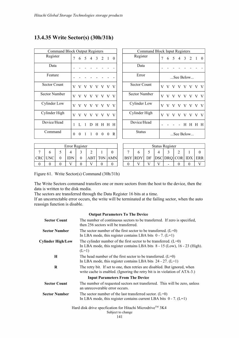
13.4.35 Write Sector(s) (30h/31h)
...See Below...StatusR0001100Command
HHHH----Device/HeadHHHHD1L1Device/Head
VVVVVVVVCylinder HighVVVVVVVVCylinder High
VVVVVVVVCylinder LowVVVVVVVVCylinder Low
VVVVVVVVSector NumberVVVVVVVVSector Number
VVVVVVVVSector CountVVVVVVVVSector Count
...See Below...Error--------Feature
--------Data--------Data
01234567Register01234567RegisterCommand Block Input RegistersCommand Block Output Registers
V00-VVV000V0V000ERRIDXCORDRQDSCDFRDYBSYAMNT0NABT0IDN0UNCCRC
0123456701234567Status RegisterError Register
Figure 61. Write Sector(s) Command (30h/31h)
The Write Sectors command transfers one or more sectors from the host to the device, then thedata is written to the disk media.The sectors are transferred through the Data Register 16 bits at a time.If an uncorrectable error occurs, the write will be terminated at the failing sector, when the autoreassign function is disable.
The sector number of the last transferred sector. (L=0)In LBA mode, this register contains current LBA bits 0 - 7. (L=1)
Sector Number
The number of requested sectors not transferred. This will be zero, unlessan unrecoverable error occurs.
Sector CountInput Parameters From The Device
The retry bit. If set to one, then retries are disabled. But ignored, whenwrite cache is enabled. (Ignoring the retry bit is in violation of ATA-3.)
R
The head number of the first sector to be transferred. (L=0)In LBA mode, this register contains LBA bits 24 - 27. (L=1)
H
The cylinder number of the first sector to be transferred. (L=0)In LBA mode, this register contains LBA bits 8 - 15 (Low), 16 - 23 (High).(L=1)
Cylinder High/Low
The sector number of the first sector to be transferred. (L=0)In LBA mode, this register contains LBA bits 0 - 7. (L=1)
Sector Number
The number of continuous sectors to be transferred. If zero is specified,then 256 sectors will be transferred.
Sector CountOutput Parameters To The Device
Hitachi Global Storage Technologies storage products
Hard disk drive specfication for Hitachi MicrodriveTM 3K4 Subject to change
141
The head number of the last transferred sector. (L=0)In LBA mode, thisregister contains current LBA bits 24 - 27. (L=1)
H
The cylinder number of the last transferred sector. (L=0)In LBA mode, this register contains current LBA bits 8 - 15 (Low), 16 - 23(High). (L=1)
Cylinder High/Low
Hitachi Global Storage Technologies storage products
Hard disk drive specfication for Hitachi MicrodriveTM 3K4 Subject to change
142
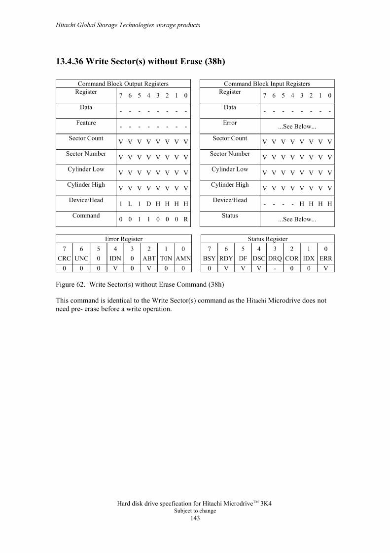
13.4.36 Write Sector(s) without Erase (38h)
...See Below...StatusR0001100Command
HHHH----Device/HeadHHHHD1L1Device/Head
VVVVVVVVCylinder HighVVVVVVVVCylinder High
VVVVVVVVCylinder LowVVVVVVVVCylinder Low
VVVVVVVVSector NumberVVVVVVVVSector Number
VVVVVVVVSector CountVVVVVVVVSector Count
...See Below...Error--------Feature
--------Data--------Data
01234567Register01234567RegisterCommand Block Input RegistersCommand Block Output Registers
V00-VVV000V0V000ERRIDXCORDRQDSCDFRDYBSYAMNT0NABT0IDN0UNCCRC
0123456701234567Status RegisterError Register
Figure 62. Write Sector(s) without Erase Command (38h)
This command is identical to the Write Sector(s) command as the Hitachi Microdrive does notneed pre- erase before a write operation.
Hitachi Global Storage Technologies storage products
Hard disk drive specfication for Hitachi MicrodriveTM 3K4 Subject to change
143
13.4.37 Write Verify (3Ch: Vendor Specific)
In implementation, Write Verify command is exactry same as Write Sector(s) command (30h).No read verification is performed after write operation.
Refer to Write Sectors Command for parameters.
Hitachi Global Storage Technologies storage products
Hard disk drive specfication for Hitachi MicrodriveTM 3K4 Subject to change
144
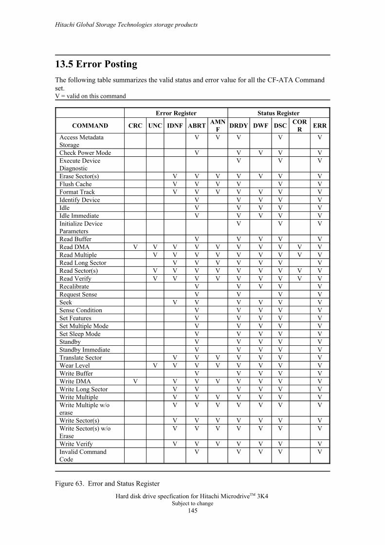
13.5 Error PostingThe following table summarizes the valid status and error value for all the CF-ATA Commandset. V = valid on this command
VVVVVInvalid CommandCode
VVVVVVVWrite Verify
VVVVVVVWrite Sector(s) w/oErase
VVVVVVVWrite Sector(s)
VVVVVVVWrite Multiple w/oerase
VVVVVVVWrite MultipleVVVVVVWrite Long SectorVVVVVVVVWrite DMAVVVVVWrite BufferVVVVVVVVWear LevelVVVVVVVTranslate SectorVVVVVStandby ImmediateVVVVVStandbyVVVVVSet Sleep ModeVVVVVSet Multiple ModeVVVVVSet FeaturesVVVVVSense ConditionVVVVVVSeekVVVVRequest SenseVVVVVRecalibrateVVVVVVVVVRead VerifyVVVVVVVVVRead Sector(s)VVVVVVVRead Long SectorVVVVVVVVVRead MultipleVVVVVVVVVVRead DMAVVVVVRead Buffer
VVVInitialize DeviceParameters
VVVVVIdle ImmediateVVVVVIdleVVVVVIdentify DeviceVVVVVVVFormat TrackVVVVVVFlush CacheVVVVVVVErase Sector(s)
VVVExecute DeviceDiagnostic
VVVVVCheck Power Mode
VVVVVAccess MetadataStorage
ERRCORRDSCDWFDRDYAMN
FABRTIDNFUNCCRCCOMMAND
Status RegisterError Register
Figure 63. Error and Status Register
Hitachi Global Storage Technologies storage products
Hard disk drive specfication for Hitachi MicrodriveTM 3K4 Subject to change
145
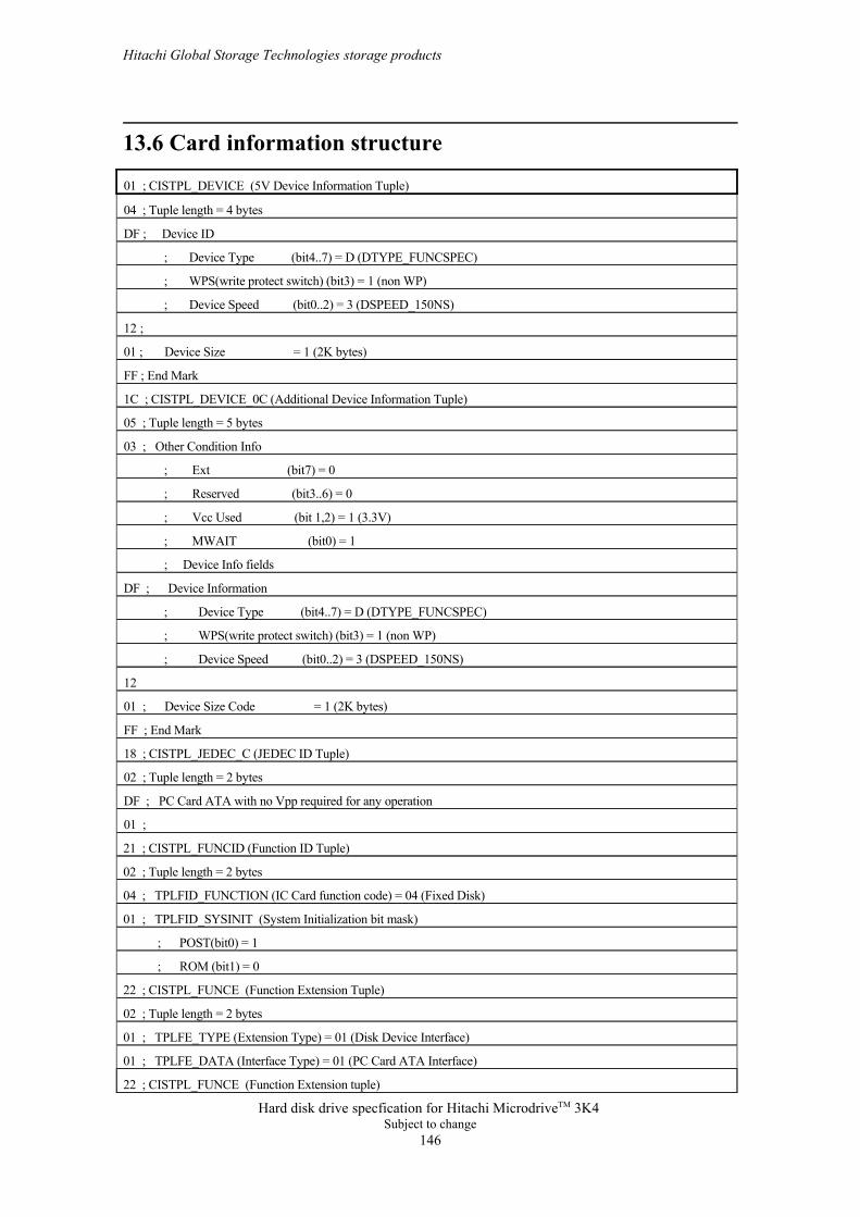
13.6 Card information structure
22 ; CISTPL_FUNCE (Function Extension tuple)
01 ; TPLFE_DATA (Interface Type) = 01 (PC Card ATA Interface)
01 ; TPLFE_TYPE (Extension Type) = 01 (Disk Device Interface)
02 ; Tuple length = 2 bytes
22 ; CISTPL_FUNCE (Function Extension Tuple)
; ROM (bit1) = 0
; POST(bit0) = 1
01 ; TPLFID_SYSINIT (System Initialization bit mask)
04 ; TPLFID_FUNCTION (IC Card function code) = 04 (Fixed Disk)
02 ; Tuple length = 2 bytes
21 ; CISTPL_FUNCID (Function ID Tuple)
01 ;
DF ; PC Card ATA with no Vpp required for any operation
02 ; Tuple length = 2 bytes
18 ; CISTPL_JEDEC_C (JEDEC ID Tuple)
FF ; End Mark
01 ; Device Size Code = 1 (2K bytes)
12
; Device Speed (bit0..2) = 3 (DSPEED_150NS)
; WPS(write protect switch) (bit3) = 1 (non WP)
; Device Type (bit4..7) = D (DTYPE_FUNCSPEC)
DF ; Device Information
; Device Info fields
; MWAIT (bit0) = 1
; Vcc Used (bit 1,2) = 1 (3.3V)
; Reserved (bit3..6) = 0
; Ext (bit7) = 0
03 ; Other Condition Info
05 ; Tuple length = 5 bytes
1C ; CISTPL_DEVICE_0C (Additional Device Information Tuple)
FF ; End Mark
01 ; Device Size = 1 (2K bytes)
12 ;
; Device Speed (bit0..2) = 3 (DSPEED_150NS)
; WPS(write protect switch) (bit3) = 1 (non WP)
; Device Type (bit4..7) = D (DTYPE_FUNCSPEC)
DF ; Device ID
04 ; Tuple length = 4 bytes
01 ; CISTPL_DEVICE (5V Device Information Tuple)
Hitachi Global Storage Technologies storage products
Hard disk drive specfication for Hitachi MicrodriveTM 3K4 Subject to change
146
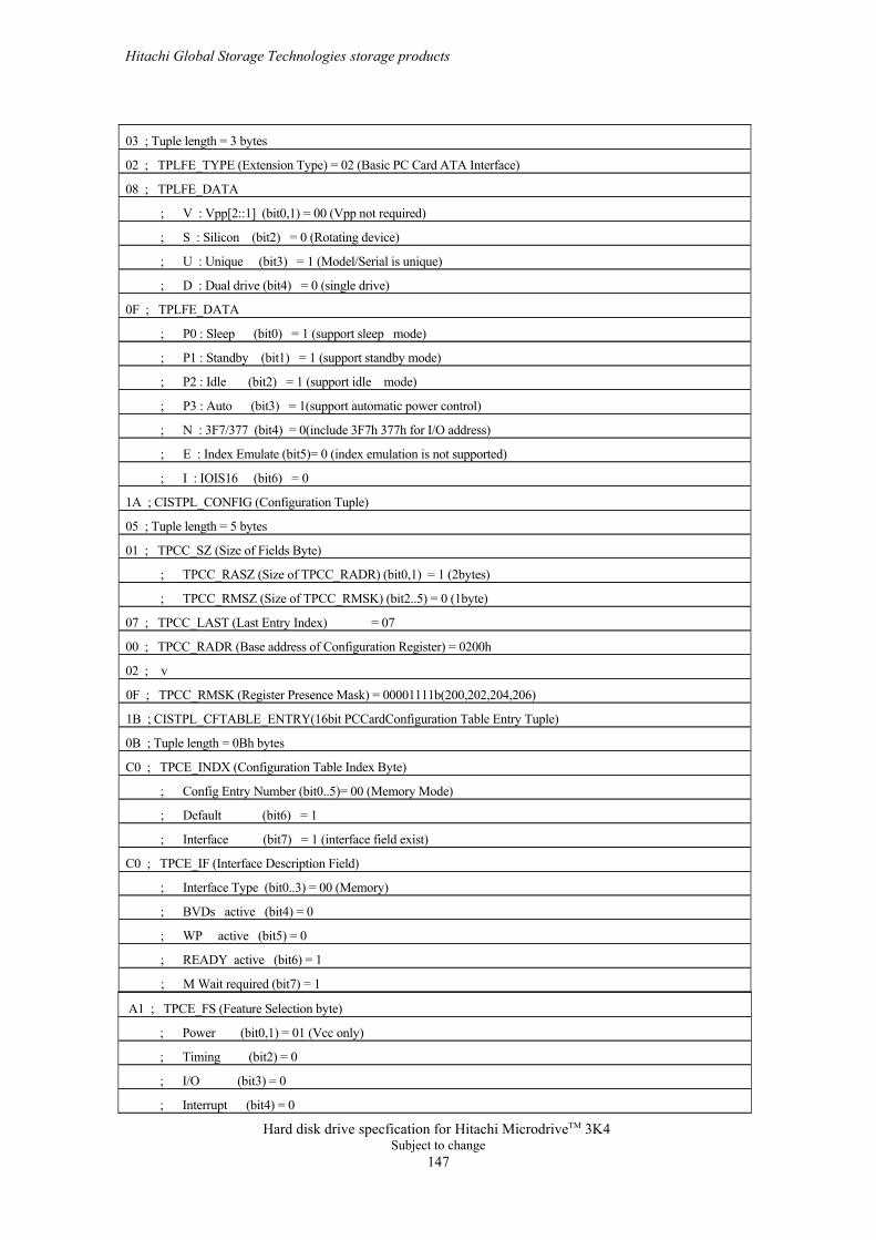
; M Wait required (bit7) = 1
; READY active (bit6) = 1
; WP active (bit5) = 0
; BVDs active (bit4) = 0
; Interface Type (bit0..3) = 00 (Memory)
C0 ; TPCE_IF (Interface Description Field)
; Interface (bit7) = 1 (interface field exist)
; Default (bit6) = 1
; Config Entry Number (bit0..5)= 00 (Memory Mode)
C0 ; TPCE_INDX (Configuration Table Index Byte)
0B ; Tuple length = 0Bh bytes
1B ; CISTPL_CFTABLE_ENTRY(16bit PCCardConfiguration Table Entry Tuple)
0F ; TPCC_RMSK (Register Presence Mask) = 00001111b(200,202,204,206)
02 ; v
00 ; TPCC_RADR (Base address of Configuration Register) = 0200h
07 ; TPCC_LAST (Last Entry Index) = 07
; TPCC_RMSZ (Size of TPCC_RMSK) (bit2..5) = 0 (1byte)
; TPCC_RASZ (Size of TPCC_RADR) (bit0,1) = 1 (2bytes)
01 ; TPCC_SZ (Size of Fields Byte)
05 ; Tuple length = 5 bytes
1A ; CISTPL_CONFIG (Configuration Tuple)
; I : IOIS16 (bit6) = 0
; E : Index Emulate (bit5)= 0 (index emulation is not supported)
; N : 3F7/377 (bit4) = 0(include 3F7h 377h for I/O address)
; P3 : Auto (bit3) = 1(support automatic power control)
; P2 : Idle (bit2) = 1 (support idle mode)
; P1 : Standby (bit1) = 1 (support standby mode)
; P0 : Sleep (bit0) = 1 (support sleep mode)
0F ; TPLFE_DATA
; D : Dual drive (bit4) = 0 (single drive)
; U : Unique (bit3) = 1 (Model/Serial is unique)
; S : Silicon (bit2) = 0 (Rotating device)
; V : Vpp[2::1] (bit0,1) = 00 (Vpp not required)
08 ; TPLFE_DATA
02 ; TPLFE_TYPE (Extension Type) = 02 (Basic PC Card ATA Interface)
03 ; Tuple length = 3 bytes
; Interrupt (bit4) = 0
; I/O (bit3) = 0
; Timing (bit2) = 0
; Power (bit0,1) = 01 (Vcc only)
A1 ; TPCE_FS (Feature Selection byte)
Hitachi Global Storage Technologies storage products
Hard disk drive specfication for Hitachi MicrodriveTM 3K4 Subject to change
147
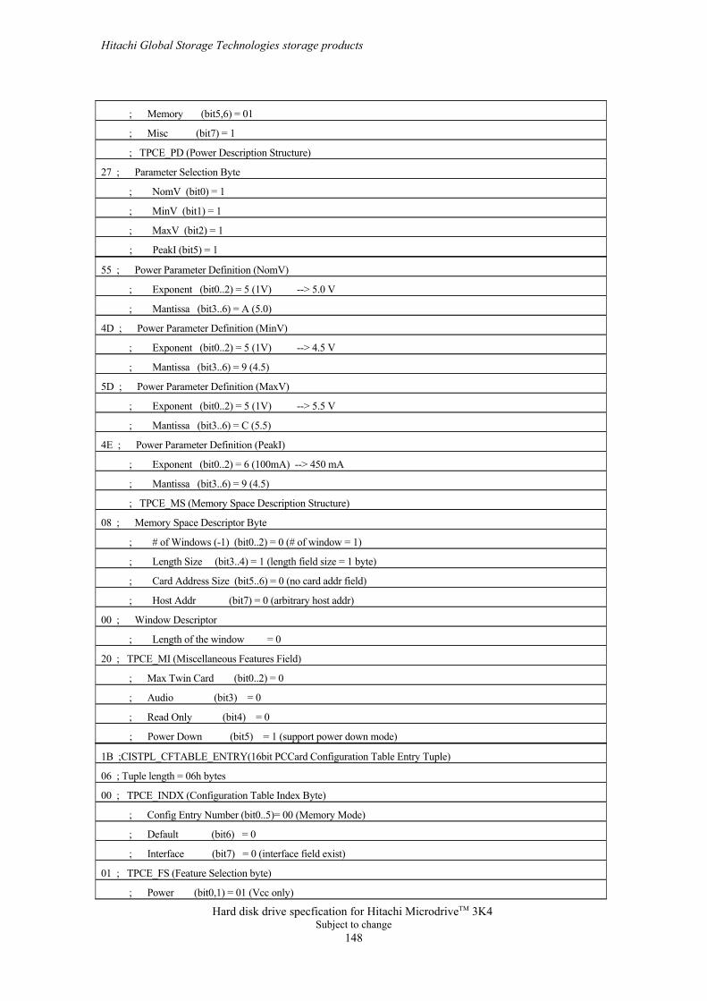
; PeakI (bit5) = 1
; MaxV (bit2) = 1
; MinV (bit1) = 1
; NomV (bit0) = 1
27 ; Parameter Selection Byte
; TPCE_PD (Power Description Structure)
; Misc (bit7) = 1
; Memory (bit5,6) = 01
; Power Down (bit5) = 1 (support power down mode)
; Read Only (bit4) = 0
; Audio (bit3) = 0
; Max Twin Card (bit0..2) = 0
20 ; TPCE_MI (Miscellaneous Features Field)
; Length of the window = 0
00 ; Window Descriptor
; Host Addr (bit7) = 0 (arbitrary host addr)
; Card Address Size (bit5..6) = 0 (no card addr field)
; Length Size (bit3..4) = 1 (length field size = 1 byte)
; # of Windows (-1) (bit0..2) = 0 (# of window = 1)
08 ; Memory Space Descriptor Byte
; TPCE_MS (Memory Space Description Structure)
; Mantissa (bit3..6) = 9 (4.5)
; Exponent (bit0..2) = 6 (100mA) --> 450 mA
4E ; Power Parameter Definition (PeakI)
; Mantissa (bit3..6) = C (5.5)
; Exponent (bit0..2) = 5 (1V) --> 5.5 V
5D ; Power Parameter Definition (MaxV)
; Mantissa (bit3..6) = 9 (4.5)
; Exponent (bit0..2) = 5 (1V) --> 4.5 V
4D ; Power Parameter Definition (MinV)
; Mantissa (bit3..6) = A (5.0)
; Exponent (bit0..2) = 5 (1V) --> 5.0 V
55 ; Power Parameter Definition (NomV)
; Power (bit0,1) = 01 (Vcc only)
01 ; TPCE_FS (Feature Selection byte)
; Interface (bit7) = 0 (interface field exist)
; Default (bit6) = 0
; Config Entry Number (bit0..5)= 00 (Memory Mode)
00 ; TPCE_INDX (Configuration Table Index Byte)
06 ; Tuple length = 06h bytes
1B ;CISTPL_CFTABLE_ENTRY(16bit PCCard Configuration Table Entry Tuple)
Hitachi Global Storage Technologies storage products
Hard disk drive specfication for Hitachi MicrodriveTM 3K4 Subject to change
148

; Mantissa (bit3..6) = 7 (3.5)
; Exponent (bit0..2) = 6 (100mA) --> 350 mA
3E ; Power Parameter Definition (PeakI)
1E ; Extension = 1Eh = +0.30 --+
; Extension (bit7) = 1 (extension exists) +
; Mantissa (bit3..6) = 6 (3.0) +
; Exponent (bit0..2) = 5 (1V) --+-> 3.3 V
B5 ; Power Parameter Definition (NomV)
; PeakI (bit5) = 1
; MaxV (bit2) = 0
; MinV (bit1) = 0
; NomV (bit0) = 1
21 ; Parameter Selection Byte
; Misc (bit7) = 0
; Memory (bit5,6) = 00
; Interrupt (bit4) = 0
; I/O (bit3) = 0
; Timing (bit2) = 0
; MinV (bit1) = 1
; NomV (bit0) = 1
27 ; Parameter Selection Byte
; TPCE_PD (Power Description Structure)
; Misc (bit7) = 1
; Memory (bit5,6) = 00
; Interrupt (bit4) = 1
; I/O (bit3) = 1
; Timing (bit2) = 0
; Power (bit0,1) = 01 (Vcc only)
99 ; TPCE_FS (Feature Selection byte)
; M Wait required (bit7) = 0
; READY active (bit6) = 1
; WP active (bit5) = 0
; BVDs active (bit4) = 0
; Interface Type (bit0..3) = 01 (I/O and Memory)
41 ; TPCE_IF (Interface Description Field)
; Interface (bit7) = 1 (interface field exist)
; Default (bit6) = 1
; Config Entry Number (bit0..5)= 01 (I/O and Memory Mode)
C1 ; TPCE_INDX (Configuration Table Index Byte)
0D ; Tuple length = 0Dh bytes
1B ;CISTPL_CFTABLE_ENTRY(16bit PCCard Configuration Table Entry Tuple)
Hitachi Global Storage Technologies storage products
Hard disk drive specfication for Hitachi MicrodriveTM 3K4 Subject to change
149
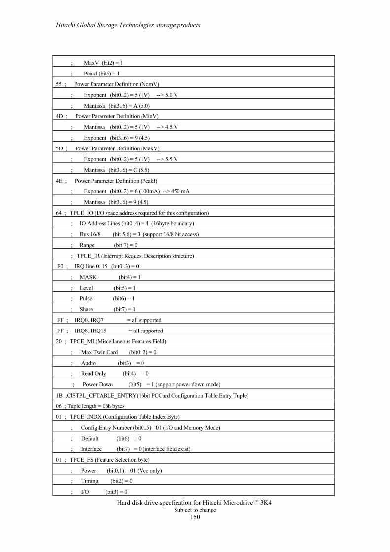
; Power Down (bit5) = 1 (support power down mode)
; Read Only (bit4) = 0
; Audio (bit3) = 0
; Max Twin Card (bit0..2) = 0
20 ; TPCE_MI (Miscellaneous Features Field)
FF ; IRQ8..IRQ15 = all supported
FF ; IRQ0..IRQ7 = all supported
; Share (bit7) = 1
; Pulse (bit6) = 1
; Level (bit5) = 1
; MASK (bit4) = 1
F0 ; IRQ line 0..15 (bit0..3) = 0
; TPCE_IR (Interrupt Request Description structure)
; Range (bit 7) = 0
; Bus 16/8 (bit 5,6) = 3 (support 16/8 bit access)
; IO Address Lines (bit0..4) = 4 (16byte boundary)
64 ; TPCE_IO (I/O space address required for this configuration)
; Mantissa (bit3..6) = 9 (4.5)
; Exponent (bit0..2) = 6 (100mA) --> 450 mA
4E ; Power Parameter Definition (PeakI)
; Mantissa (bit3..6) = C (5.5)
; Exponent (bit0..2) = 5 (1V) --> 5.5 V
5D ; Power Parameter Definition (MaxV)
; Exponent (bit3..6) = 9 (4.5)
; Mantissa (bit0..2) = 5 (1V) --> 4.5 V
4D ; Power Parameter Definition (MinV)
; Mantissa (bit3..6) = A (5.0)
; Exponent (bit0..2) = 5 (1V) --> 5.0 V
55 ; Power Parameter Definition (NomV)
; PeakI (bit5) = 1
; MaxV (bit2) = 1
; I/O (bit3) = 0
; Timing (bit2) = 0
; Power (bit0,1) = 01 (Vcc only)
01 ; TPCE_FS (Feature Selection byte)
; Interface (bit7) = 0 (interface field exist)
; Default (bit6) = 0
; Config Entry Number (bit0..5)= 01 (I/O and Memory Mode)
01 ; TPCE_INDX (Configuration Table Index Byte)
06 ; Tuple length = 06h bytes
1B ;CISTPL_CFTABLE_ENTRY(16bit PCCard Configuration Table Entry Tuple)
Hitachi Global Storage Technologies storage products
Hard disk drive specfication for Hitachi MicrodriveTM 3K4 Subject to change
150
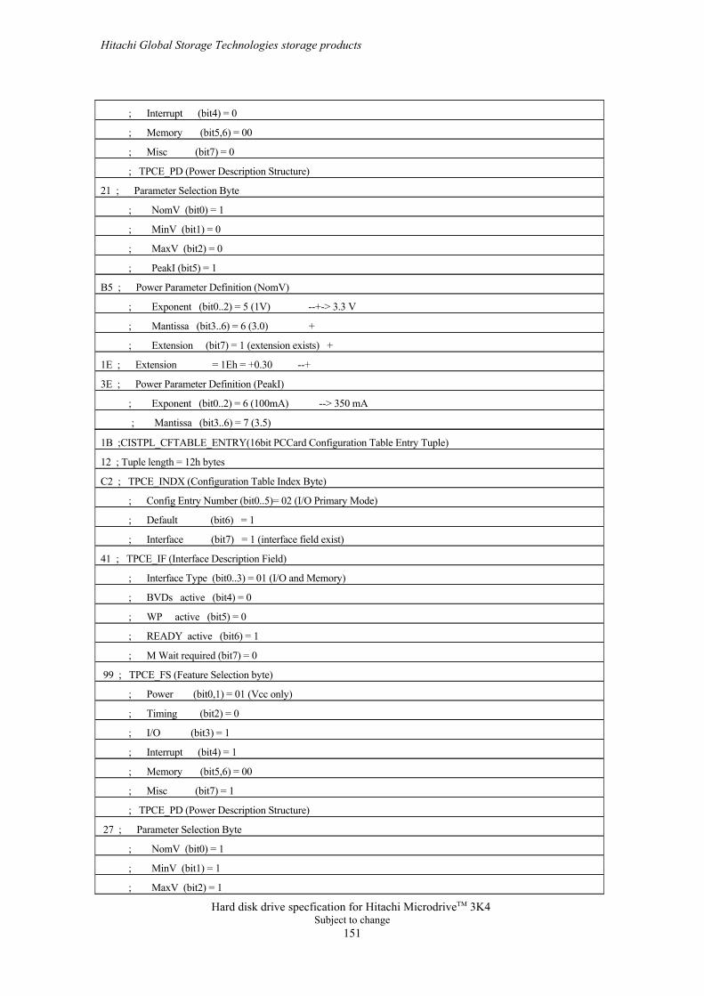
; Mantissa (bit3..6) = 7 (3.5)
; Exponent (bit0..2) = 6 (100mA) --> 350 mA
3E ; Power Parameter Definition (PeakI)
1E ; Extension = 1Eh = +0.30 --+
; Extension (bit7) = 1 (extension exists) +
; Mantissa (bit3..6) = 6 (3.0) +
; Exponent (bit0..2) = 5 (1V) --+-> 3.3 V
B5 ; Power Parameter Definition (NomV)
; PeakI (bit5) = 1
; MaxV (bit2) = 0
; MinV (bit1) = 0
; NomV (bit0) = 1
21 ; Parameter Selection Byte
; TPCE_PD (Power Description Structure)
; Misc (bit7) = 0
; Memory (bit5,6) = 00
; Interrupt (bit4) = 0
; MaxV (bit2) = 1
; MinV (bit1) = 1
; NomV (bit0) = 1
27 ; Parameter Selection Byte
; TPCE_PD (Power Description Structure)
; Misc (bit7) = 1
; Memory (bit5,6) = 00
; Interrupt (bit4) = 1
; I/O (bit3) = 1
; Timing (bit2) = 0
; Power (bit0,1) = 01 (Vcc only)
99 ; TPCE_FS (Feature Selection byte)
; M Wait required (bit7) = 0
; READY active (bit6) = 1
; WP active (bit5) = 0
; BVDs active (bit4) = 0
; Interface Type (bit0..3) = 01 (I/O and Memory)
41 ; TPCE_IF (Interface Description Field)
; Interface (bit7) = 1 (interface field exist)
; Default (bit6) = 1
; Config Entry Number (bit0..5)= 02 (I/O Primary Mode)
C2 ; TPCE_INDX (Configuration Table Index Byte)
12 ; Tuple length = 12h bytes
1B ;CISTPL_CFTABLE_ENTRY(16bit PCCard Configuration Table Entry Tuple)
Hitachi Global Storage Technologies storage products
Hard disk drive specfication for Hitachi MicrodriveTM 3K4 Subject to change
151
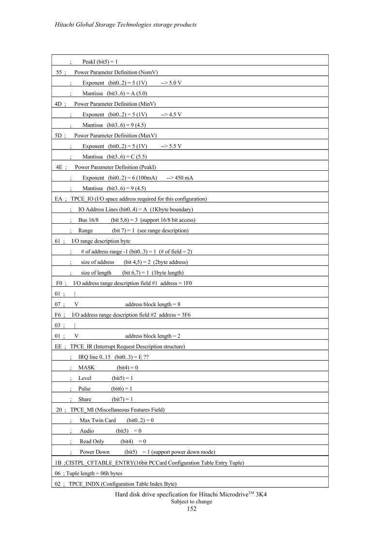
; Power Down (bit5) = 1 (support power down mode)
; Read Only (bit4) = 0
; Audio (bit3) = 0
; Max Twin Card (bit0..2) = 0
20 ; TPCE_MI (Miscellaneous Features Field)
; Share (bit7) = 1
; Pulse (bit6) = 1
; Level (bit5) = 1
; MASK (bit4) = 0
; IRQ line 0..15 (bit0..3) = E ??
EE ; TPCE_IR (Interrupt Request Description structure)
01 ; V address block length = 2
03 ; |
F6 ; I/O address range description field #2 address = 3F6
07 ; V address block length = 8
01 ; |
F0 ; I/O address range description field #1 address = 1F0
; size of length (bit 6,7) = 1 (1byte length)
; size of address (bit 4,5) = 2 (2byte address)
; # of address range -1 (bit0..3) = 1 (# of field = 2)
61 ; I/O range description byte
; Range (bit 7) = 1 (see range description)
; Bus 16/8 (bit 5,6) = 3 (support 16/8 bit access)
; IO Address Lines (bit0..4) = A (1Kbyte boundary)
EA ; TPCE_IO (I/O space address required for this configuration)
; Mantissa (bit3..6) = 9 (4.5)
; Exponent (bit0..2) = 6 (100mA) --> 450 mA
4E ; Power Parameter Definition (PeakI)
; Mantissa (bit3..6) = C (5.5)
; Exponent (bit0..2) = 5 (1V) --> 5.5 V
5D ; Power Parameter Definition (MaxV)
; Mantissa (bit3..6) = 9 (4.5)
; Exponent (bit0..2) = 5 (1V) --> 4.5 V
4D ; Power Parameter Definition (MinV)
; Mantissa (bit3..6) = A (5.0)
; Exponent (bit0..2) = 5 (1V) --> 5.0 V
55 ; Power Parameter Definition (NomV)
; PeakI (bit5) = 1
02 ; TPCE_INDX (Configuration Table Index Byte)
06 ; Tuple length = 06h bytes
1B ;CISTPL_CFTABLE_ENTRY(16bit PCCard Configuration Table Entry Tuple)
Hitachi Global Storage Technologies storage products
Hard disk drive specfication for Hitachi MicrodriveTM 3K4 Subject to change
152
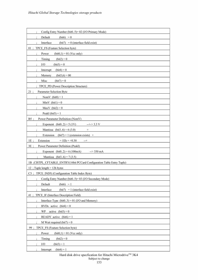
; Mantissa (bit3..6) = 7 (3.5)
; Exponent (bit0..2) = 6 (100mA) --> 350 mA
3E ; Power Parameter Definition (PeakI)
1E ; Extension = 1Eh = +0.30 --+
; Extension (bit7) = 1 (extension exists) +
; Mantissa (bit3..6) = 6 (3.0) +
; Exponent (bit0..2) = 5 (1V) --+-> 3.3 V
B5 ; Power Parameter Definition (NomV)
; PeakI (bit5) = 1
; MaxV (bit2) = 0
; MinV (bit1) = 0
; NomV (bit0) = 1
21 ; Parameter Selection Byte
; TPCE_PD (Power Description Structure)
; Misc (bit7) = 0
; Memory (bit5,6) = 00
; Interrupt (bit4) = 0
; I/O (bit3) = 0
; Timing (bit2) = 0
; Power (bit0,1) = 01 (Vcc only)
01 ; TPCE_FS (Feature Selection byte)
; Interface (bit7) = 0 (interface field exist)
; Default (bit6) = 0
; Config Entry Number (bit0..5)= 02 (I/O Primary Mode)
; Interrupt (bit4) = 1
; I/O (bit3) = 1
; Timing (bit2) = 0
; Power (bit0,1) = 01 (Vcc only)
99 ; TPCE_FS (Feature Selection byte)
; M Wait required (bit7) = 0
; READY active (bit6) = 1
; WP active (bit5) = 0
; BVDs active (bit4) = 0
; Interface Type (bit0..3) = 01 (I/O and Memory)
41 ; TPCE_IF (Interface Description Field)
; Interface (bit7) = 1 (interface field exist)
; Default (bit6) = 1
; Config Entry Number (bit0..5)= 03 (I/O Secondary Mode)
C3 ; TPCE_INDX (Configuration Table Index Byte)
12 ; Tuple length = 12h bytes
1B ;CISTPL_CFTABLE_ENTRY(16bit PCCard Configuration Table Entry Tuple)
Hitachi Global Storage Technologies storage products
Hard disk drive specfication for Hitachi MicrodriveTM 3K4 Subject to change
153
20 ; TPCE_MI (Miscellaneous Features Field)
; Share (bit7) = 1
; Pulse (bit6) = 1
; Level (bit5) = 1
; MASK (bit4) = 0
; IRQ line 0..15 (bit0..3) = E
EE ; TPCE_IR (Interrupt Request Description structure)
01 ; V address block length = 2
03 ; |
76 ; I/O address range description field #2 address = 376
07 ; V address block length = 8
01 ; |
70 ; I/O address range description field #1 address = 170
; size of length (bit 6,7) = 1 (1byte length)
; size of address (bit 4,5) = 2 (2byte address)
; # of address range -1 (bit0..3) = 1 (# of field = 2)
61 ; I/O range description byte
; Range (bit 7) = 1 (see range description)
; Bus 16/8 (bit 5,6) = 3 (support 16/8 bit access)
; IO Address Lines (bit0..4) = A (1Kbyte boundary)
EA ; TPCE_IO (I/O space address required for this configuration)
; Mantissa (bit3..6) = 9 (4.5)
; Exponent (bit0..2) = 6 (100mA) --> 450 mA
4E ; Power Parameter Definition (PeakI)
; Mantissa (bit3..6) = C (5.5)
; Exponent (bit0..2) = 5 (1V) --> 5.5 V
5D ; Power Parameter Definition (MaxV)
; Mantissa (bit3..6) = 9 (4.5)
; Exponent (bit0..2) = 5 (1V) --> 4.5 V
4D ; Power Parameter Definition (MinV)
; Mantissa (bit3..6) = A (5.0)
; Exponent (bit0..2) = 5 (1V) --> 5.0 V
55 ; Power Parameter Definition (NomV)
; PeakI (bit5) = 1
; MaxV (bit2) = 1
; MinV (bit1) = 1
; NomV (bit0) = 1
27 ; Parameter Selection Byte
; TPCE_PD (Power Description Structure)
; Misc (bit7) = 1
; Memory (bit5,6) = 00
Hitachi Global Storage Technologies storage products
Hard disk drive specfication for Hitachi MicrodriveTM 3K4 Subject to change
154
; Power Down (bit5) = 1 (support power down mode)
; Read Only (bit4) = 0
; Audio (bit3) = 0
; Max Twin Card (bit0..2) = 0
01 ; Minor Version = 1 V
04 ; Major Version = 4 ( JEIDA 4.2/PCMCIA 2.1 )
12 ; tuple length = 12h ( 18 ) bytes
15 ; CISTPL_VERS_1 ( level1 Version Tuple )
00 ; V
00 ; TPLMID_CARD ( Manufacture Info )
00 ; V
07 ; TPLMID_MANF ( Manufacture Code ) = 0319h for Hitachi
04 ; Tuple length = 4 bytes
20 ; CISTPL_MANFID ( Manufacture ID Tuple )
; Mantissa (bit3..6) = 7 (3.5)
; Exponent (bit0..2) = 6 (100mA) --> 350 mA
3E ; Power Parameter Definition (PeakI)
1E ; Extension = 1Eh = +0.30 --+
; Extension (bit7) = 1 (extension exists) +
; Mantissa (bit3..6) = 6 (3.0) +
; Exponent (bit0..2) = 5 (1V) --+-> 3.3 V
B5 ; Power Parameter Definition (NomV)
; PeakI (bit5) = 1
; MaxV (bit2) = 0
; MinV (bit1) = 0
; NomV (bit0) = 1
21 ; Parameter Selection Byte
; TPCE_PD (Power Description Structure)
; Misc (bit7) = 0
; Memory (bit5,6) = 00
; Interrupt (bit4) = 0
; I/O (bit3) = 0
; Timing (bit2) = 0
; Power (bit0,1) = 01 (Vcc only)
01 ; TPCE_FS (Feature Selection byte)
; Interface (bit7) = 0 (interface field exist)
; Default (bit6) = 0
; Config Entry Number (bit0..5)= 03 (I/O Secondary Mode)
03 ; TPCE_INDX (Configuration Table Index Byte)
06 ; Tuple length = 06h bytes
1B ;CISTPL_CFTABLE_ENTRY(16bit PCCard Configuration Table Entry Tuple)
Hitachi Global Storage Technologies storage products
Hard disk drive specfication for Hitachi MicrodriveTM 3K4 Subject to change
155
FF ; End Mark
00
65 ; "e"
76 ; "v"
69 ; "i"
72 ; "r"
64 ; "d"
6F ; "o"
72 ; "r"
63 ; "c"
69 ; "i"
6D ; "m"
00
49 ; "I"
48 ; "H"
43 ; "C"
41 ; "A"
54 ; "T"
49 ; "I"
48 ; "H"
00 ; Tuple length = 0 bytes
14 ; CISTPL_NO_LINK (No Link Tuple)
FF ; CISTPL_END (Tuple End)
Hitachi Global Storage Technologies storage products
Hard disk drive specfication for Hitachi MicrodriveTM 3K4 Subject to change
156
© Copyright Hitachi Global Storage Technologies
Hitachi Global Storage Technologies5600 Cottle RoadSan Jose, CA 95193Produced in the United States
10/03
All rights reserved Travelstar™ is a trademark ofHitachi Global Storage Technologies.
Microsoft, Windows XP, and Windows are trademarks of Microsoft Corporation in the United States, other countries, or both.
Other product names are trademarks or registered trade-marks of their respective companies. References in this publication to Hitachi Global Storage Technologies products, programs or services do not imply that Hitachi Global Storage Technologies intends to make these available in all countries in which Hitachi Global Storage Technologies operates.
Product information is provided for information pur-poses only and does not constitute a warranty. Information is true as of the date of publication and is subject to change. Actual results may vary. This publication is for general guidance only. Photo-graphs may show design models.
17 October 2003