Embed Size (px)
Citation preview

HARDWARE DESIGN AND IMPLEMENTATION FOR A WIRELESS
DISTRIBUTED INTELLIGENT SYSTEM UTILIZING 802.1 1
Gary Wong
B.A.Sc. (Honors), Simon Fraser University, 2000
A PROJECT SUBMITTED IN PARTIAL FULFILLMENT OF
THE REQUIREMENTS FOR THE DEGREE OF
MASTER OF ENGINEERING
In the School
of
Engineering Science
O Gary Wong 2004
SIMON FRASER UNIVERSITY
Fa11 2004
All rights reserved. This work may not be reproduced in whole or in part,
by photocopy or other means, without permission of the author.
APPROVAL
Name:
Degree:
Title of Project:
Gary Wong
Master of Engineering
Hardware Design and Implementation for a
Wireless Intelligent System Utilizing 802.1 1
Examining Committee:
W. A. Gruver Senior Supervisor Professor
D. Sabaz Chief Technology Officer Intelligent Robotics Manufacturing and Systems
Date Approved:
. &&

SIMON FRASER UNIVERSITY
PARTIAL COPYRIGHT LICENCE
The author, whose copyright is declared on the title page of this work, has granted to Simon Fraser University the right to lend this thesis, project or extended essay to users of the Simon Fraser University Library, and to make partial or single copies only for such users or in response to a request from the library of any other university, or other educational institution, on its own behalf or for one of its users.
The author has further granted permission to Simon Fraser University to keep or make a digital copy for use in its circulating collection.
The author has further agreed that permission for multiple copying of this work for scholarly purposes may be granted by either the author or the Dean of Graduate Studies.
It is understood that copying or publication of this work for financial gain shall not be allowed without the author's written permission. \
Permission for public performance, or limited permission for private scholarly use, of any multimedia materials forming part of this work, may have been granted by the author. This information may be found on the separately catalogued multimedia material and in the signed Partial Copyright Licence.
The original Partial Copyright Licence attesting to these terms, and signed by this author, may be found in the original bound copy of this work, retained in the Simon Fraser University Archive.
W. A. C. Bennett Library Simon Fraser University
Burnaby, BC, Canada

ABSTRACT
Wireless devices using the IEEE 802.1 1 standard have two inherent fundamental
limitations. The range of wireless devices themselves, entailing a point-to-point
communication channel, constricts the area of coverage. Secondly, the standard only
provides for a wireless communication path connecting devices, no facility is available
for users to implement services at each wireless device
To overcome these deficiencies, a separate subsystem that can be controlled and
enhanced with added computational sub-systems is constructed. By introducing the
ability to control the wireless module with supporting hardware and firmware, the extra
intelligence required to implement peer-to-peer connectivity and the facility for users to
introduced distributed intelligence. With these additions, wireless infrastructures that are
truly scalable and distributed will be possible.
This report will outline the design of a wireless device that will enable higher level
systems to facilitate a wireless network that will be totally peer-to-peer and the ability to
incorporate distributed intelligence.
iii

DEDICATION
This work is dedicated to my family
for their unconditional love and support
in all aspects of my life.

ACKNOWLEDGEMENTS
The author would like to express his gratitude and appreciation to Dr. W. A. Gruver and
Mr. D. Sabaz for their support, understanding, and knowledge. Their supervisory roles
throughout the execution of this project are thankfully acknowledged.

TABLE OF CONTENTS . . .................................................................................................................... APPROVAL 11 ... ABSTRACT ................................................................................................................... III
................................................................................................................. DEDICATION iv
ACKNOWLEDGEMENTS ............................................................................................... v
TABLE OF CONTENTS ................................................................................................. vi ... LIST OF FIGURES ....................................................................................................... VIII
ABBREVIATIONS AND ACRONYMS ........................................................................... ix
INTRODUCTION ........................................................................................................ 1 1 . 1 Future of Wireless ............................................................................................. 1 1.2 Problem Definition ............................................................................................. 2
............................................................................................... 1.3 Project Overview 2
SPECIFICATION BACKGROUND ............................................................................. 3 2.1 The Advanced RlSC Machine Architecture ....................................................... 3 2.2 IEEE 802.1 1 ...................................................................................................... 4
2.2.1 General Architecture .................................................................................. 4 2.2.2 Physical Layer ............................................................................................ 6
............................................................................................ 2.2.3 MAC Sublayer 6 2.2.4 Distributed Coordination Function .............................................................. 7 2.2.5 Point Coordination Function ....................................................................... 9
DESIGN REQUIREMENTS ...................................................................................... 12 3.1 CPU ................................................................................................................ 12 3.2 Memory ........................................................................................................... 12 3.3 Video Output ................................................................................................... 13 3.4 Wireless Communication ................................................................................. 13 3.5 Inputs Interfaces .............................................................................................. 13 3.6 Miscellaneous 10 ............................................................................................. 13
ARCHITECTURE ..................................................................................................... 14 4.1 Processor ........................................................................................................ 15 4.2 Companion Chip ............................................................................................. 16
........................................................ 4.3 Power Supply Regulation and Monitoring 16 4.3.1 Setting the Main Output Voltage ............................................................... 17
............................................................... 4.3.2 Setting the Core Output Voltage 17 ........................................................................... 4.3.3 Setting the Current Limit 17
........................................................... 4.3.4 Setting the Voltage Monitor Levels 17 .................................................................................... 4.3.5 Inductor Selection 18 ..................................................................................... 4.3.6 Power Monitoring 18
4.4 Flash ROM ...................................................................................................... 18 4.5 Synchronous Dynamic RAM ............................................................................ 19
.................................................................................................. 4.6 Video Display 19 4.7 RS-232 Port .................................................................................................... 20
5 PCB and Layer Stack .............................................................................................. 21
............................................................................................. 6 OPERATING SYSTEM 22
7 CONCLUSION ......................................................................................................... 23 7.1 Future Work .................................................................................................... 23
APPENDIX .................................................................................................................... 24
.............................................................................................................. REFERENCES 35
LIST OF FIGURES
Figure 2-1: IBSS / Ad Hoc Network ................................................................................. 5
Figure 2-2: ESS Infrastructure Network ........................................................................... 6
Figure 2-3: Example of DCF Operation ........................................................................... 9
Figure 2-4: Example of PCF Operation .......................................................................... 10
Figure 4-1 : System Block Diagram ................................................................................ 14
.............................................................. Figure 4-2: PXA255 Processor Block Diagram 15
Figure 4-3: JTAG Wiring Diagram ................................................................................. 19
Figure 5-1 : PCB Layer Stack ......................................................................................... 21
Figure 7-1 : PXA255 Schematic ..................................................................................... 25
Figure 7-2: Flash Schematic .......................................................................................... 26
Figure 7-3: SDRAM Schematic ...................................................................................... 27
Figure 7-4: SA-1 11 1 Main Schematic ............................................................................ 28
Figure 7-5: Video Schematic ........................................................................................ 29
Figure 7-6: SA-1 11 1 PCMCIA Schematic ...................................................................... 30
...................................................... Figure 7-7: SA-1 11 1 Keyboard & Mouse Schematic 31
...................................................................................... Figure 7-8: RS-232 Schematic 32
Figure 7-9: Power Supply Schematic ............................................................................. 33
Figure 7-1 0: PCB Layout ............................................................................................... 34
viii

ABBREVIATIONS AND ACRONYMS
AC'97
ACK
AP
ARM
BSA
BSS
ClSC
CF
CPU
CSMAICA
CTS
CW
DCF
DlFS
DS
DSSS
ESS
FHSS
FR-4
GPlO
12c l BSS
IEEE
10
I R
KB
LAN
LCD
LED
mBGA
Audio Codec '97
Acknowledgement
Access Point
Advanced RlSC Machine
Basic Service Area
Basic Service Set
Complex Instruction Set Computer
Compact Flash
Central Processing Unit
Carrier Sense Multiple Access with Collision Avoidance
Clear-to-Send
Contention Window
Distributed Coordination Function
DCF Interframe Space
Distributed System
Direct Sequence Spread Spectrum
Extended Service Set
Frequency Hopping Spread Spectrum
Fire-Retardant 4
General Purpose Input-Output
Inter-Integrated Circuit
Independent Basic Service Set
Institute of Electrical and Electronics Engineers
Input-Output
l nf rared
Kilobyte
Local Area Network
Liquid Crystal Display
Light Emitting Diodes
micro-BGA

MC
MMC
MS
MSDU
NAV
PC
PCB
PCMCIA
PDA
PlFS
PLL
PS/2
PWM
RlSC
RAM
ROM
RF
RTS
SDRAM
Sl FS
SMROM
SRAM
SSlD
SSP
TBTT
UART
USB
VGA
W LAN
Memory Controller
Matched Memory Cycle
Mobile Station
MAC Service Data Unit
Network Allocation Vector
Personal Computer
Printed Circuit Board
Personal Computer Memory Card International Association
Personal Digital Assistant
PCF lnterframe Space
Phase-Locked Loop
Programming System 2
Pulse Width Modulation
Reduced Instruction Set Computer
Random Access Memory
Read-only Memory
Radio Frequency
Request-to-Send
Synchronous Dynamic RAM
Short lnterframe Space
Synchronous Mask ROM
Static RAM
Service Set Identifier
Speech Service Platform
Target Beacon Transition Time
Universal Asynchronous Receiver Transmitter
Universal Serial Bus
Video Graphics Array
Wireless Local Area Network

1 INTRODUCTION
1.1 Future of Wireless
Advancement in microchip technology has resulted in cheaper, smaller, higher
performing central processor units (CPUs) with low-power consumption. Size and price,
once considered major barriers for wireless technologies aimed at the consumer level,
have now spawned a society for items that are small, slim, portable and cosmetically
sexy but yet powerful. Be it a cellular phone, a Personal Digital Assistant (PDA), or a
notebook with a wireless lnternet connection, societies increasing demand for fast,
reliable, data and information services show no sign of slowing down.
Cellular phones that once only provided analog voice communications now allow the
user to surf the web, take photograph, email them to friends, and more. The PDA, once
only supplied contact information and schedule management, have become a powerful
portable computer of its own, capable of performing any task a typical desktop Personal
Computer (PC) can do.
More and more people at home and office settings are choosing wireless over
conventionally wired networks. Unlike its predecessor, wired Local Area Networks
(LAN), Wireless Local Area Networks (WLAN) have the convenience of mobility and
removes the problem of wire clutter. However, the items mentioned are not truly mobile
in the sense they are constricted to an area of service. A future with an lnternet similar
to today's but without all the wires is not only foreseeable but a certainty.

1.2 Problem Definition
Today's computers are non-intelligent but are great workers. Albeit a node in a network
that routes traffic or a computer that is used to crunch large amounts of data, they all
lack intelligence, in the sense they can do what they were designed to do but lack the
capability to learn and go beyond that scope. The goal is to have countless intelligent
mobile units that can learn and teach other new things.
1.3 Project Overview
This project will outline the hardware design and construction of a wireless device that
will enable higher level systems to facilitate a wireless network that will be totally peer-to-
peer and the ability to incorporate distributed intelligence.
2 SPECIFICATION BACKGROUND
The Advanced RlSC Machine (ARM) and IEEE 802.1 1 standard play a large part of the
project work. This section provides some background knowledge to the reader.
2.1 The Advanced RlSC Machine Architecture
Sometime in the early 1980s, between 1983 and 1985, Acorn Computers Limited of
Cambridge, England developed the first ARM processor. At the time, the market lacked
a commercial 16-bit processor with comparable latency to Acorn's own 8-bit 6502 based
microcomputer. The top-of-the-line 16-bit commercial Complex lnstruction Set
Computers (CSIC) microprocessors ran at slower clock rates then the memory while
complex instructions took several clock cycles to execute. Thus, Acorn was driven to
produce an in-house proprietary microprocessor to solve this issue.
The task was not an easy one. Acorn knew that it would require hundreds of man-years
of design effort. Having roughly 400 employees, Acorn knew the only way to succeed
was to design a more efficient commercial microprocessor with a fraction of the effort.
The situation seemed impossible until they discovered some papers written by some
post-graduate students from Berkeley.
The Berkeley Reduced lnstruction Set Computer (RISC) I was designed in less than a
year and had similar performance to current commercial microprocessors. Instead of
using many complex instructions as possible, to increase compiling time for high level
languages, the Berkeley RlSC I approach provided only a few simple instructions, each

completing within one clock cycle. To handle the complex operations, the group broke
the instruction down to subroutines.
The ARM incorporated the RlSC 1's load-and-store architecture, a fixed-length 32-bit
instruction, 3 address instruction formats and excluded the register windows, single
cycle execution, and delayed branches either due to cost or complexity.
2.2 IEEE 802.1 1
IEEE 802.1 1 standard, ratified in 1997, defines a wireless local area network
architecture that can be viewed as a wired Ethernet network (IEEE 802.2) to application
layers or layers above it. The original specification supported 1 Mbps and 2Mbps
transfer rates and now we see rates of 54Mbps and higher currently in the market place.
2.2.1 General Architecture
In an IEEE 802.1 1 network architecture, a group of mobile stations (MSes) or devices
controlled under a distribution system (DS) is called a Basic Service Set (BSS). A BSS,
which occupies a Basic Service Area (BSA), can be either an Independent Basic Service
Set (IBSS) ad hoc network or an infrastructure network. The BSA allows any station to
directly communicate with any other station (Figure 2-l), via a centralized Access Point
W ) .

mobile s t a t i o n 2
mobile s t a t i o n 3
moblle s t a t i o n 4
mobile s t a t i o n 1
Figure 2-1 : IBSS / Ad Hoc Network
In an infrastructure network, BSSes can have an extended range via inter-
communication of APs from different BSSes. This extended infrastructure is called an
Extended Service Set (ESS), and can also provide access to wired networks via portals.
Figure 2-2 illustrates an exemplary infrastructure network. The DS is analogous to a
backbone network responsible for the MAC level transport of MAC Service Data Units
(MSDUs).

mobile s t a t i o n I / AP _ - 'ix.,
moblle s t a t i o n 6
ESS
Figure 2-2: ESS Infrastructure Network
2.2.2 Physical Layer
The physical layer is responsible for transmitting and receiving packets over the wireless
medium. IEEE 802.1 1 consists of three physical layer specifications: Frequency
Hopping Spread Spectrum (FHSS), Direct Sequence Spread Spectrum (DSSS), and
Infrared (IR).
2.2.3 MAC Sublayer
The MAC sublayer is responsible for channel allocation, protocol data unit addressing,
frame formatting, error checking, and fragmentation and reassembly. The transmission
medium can be in contention or non-contention mode. During contentional periods, all
stations contend for the channel for each packet transmitted while during contention-free
6

periods, the medium usage is mediated by the AP, which eliminates stations contending
for channel access. The medium must alternate between contention periods and
contention-free periods, with long enough duration in the contention period to transmit at
least one MSDU under Distributed Coordination Function (DCF). A contention-free
period followed by a contention period is commonly referred as a superframe.
IEEE 802.1 1 supports three different types of frames: management, control, and data.
The management frames maintain timing and synchronization, handles authentication
and deauthentication, and are used for station association and disassociation with the
AP. A management frame sent at the beginning of each superframe, referred to as a
beacon frame, is used to maintain the synchronization of local timers in the stations and
deliver protocol related parameters. The beacon frame also contains the Target Beacon
Transition Time (TBTT), which indicates when the next beacon frame will arrive. Control
frames are used for handshaking and positive acknowledgments during the contention
period, and to indicate an end the contention-free period. Data frames, on the other
hand, are only used to transmit data.
2.2.4 Distributed Coordination Function
Distributed Coordination Function is the fundamental 802.1 1 MAC protocol and uses
Carrier Sense Multiple Access with Collision Avoidance (CSMNCA) on top of the
physical layer. CSMNCA is a contention-based "listen-before-talk" scheme for
transmission of MSDUs over the wireless medium to reduce the statistical probability of
collisions. Before transmitting a frame, each station must sense the channel for a
minimum duration called the DCF lnterframe Space (DIFS) followed by a random
backoff time. The random backoff time is always a multiple of a slot time. The channel

must stay idle during the entire process before the frame transmission can be initiated.
Each station maintains a contention window (CW) that determines the remaining number
of slot times a station must wait before transmission. When a station transmits an
MSDU, a duration field is set in the MAC header indicating the time the channel will be
busy with the current transaction. Based on these fields, stations detecting MSDUs sent
update their Network Allocation Vectors (NAVs). The NAV indicates the amount of time
remaining for the current transmission session to complete, before the channel will be
idle once again.
In the case of multiple DCF stations, priority is given to the station with the shortest wait
time. The remaining stations keep the same random backoff, but continue to count
down the remaining slots as soon as the channel is idle. This allows waiting stations
higher priority when they resume transmission attempt over newly initiated transmission
attempts. A collision will occur when two or more stations simultaneously count down to
zero. In this case, each transmitting station must re-transmit with a new backoff time.
The receiving station acknowledges a successful transmission with an acknowledge
frame (ACK) after a Short Interframe Space (SIFS), shorter than the DIFS. The sender
then does another random backoff, called a "post-backoff", even if there are no more
MSDUs to be delivered. If the transmission fails, no ACK is received by the sending
station, the transmission is retried with a doubled CW, reducing the probability of
collisions with other stations.
The maximum MSDU size is 2304 bytes. Frames longer than 2304 bytes are
fragmented into smaller frames and sent individually, following the same collision
avoidance scheme. As an alternative option to avoid wasted bandwidth due to collisions
8

with longer frames, a Request-to-Send (RTS) frame, followed by a Clear-to-Send (CTS)
response, can be sent to reserve a channel prior to sending a long frame. RTS and CTS
frames also contain duration fields for other stations to update their NAVs.
Figure 2-3 shows the timing for a possible DCF scenario.
MSOl I Data I
Other MSes N AV
Figure 2-3: Example of DCF Operation
2.2.5 Point Coordination Function
In IEEE 802.1 1, the Point Coordination Function has a higher priority than the DCF.
This is because a PCF can initiate transmission after a PCF Interframe Space (PIFS)
which is shorter than a DlFS but still longer than a SIFS. The PCF is a central controlled
access method coordinated by a point coordinator within the Access Point (AP) in each
BSS. PCF is optionally supported but has great benefits to time-bounded services such
as audio or video applications. The point coordinator polls stations during the collision-
free periods to transmit without contending for the channel.

The duration of the collision-free period interval is an integral multiple of the beacon
frame period. This interval length is determined by the AP to best manage the traffic.
During the collision-free period, all stations in the BSS update their NAVs to the length of
collision-free period, and may only transmit when polled by the point coordinator or when
sending an ACK frame following reception of data frame.
In a PCF sequence during a collision-free period, the point coordinator polls a station for
pending data. If the polled station has a frame to send, then it may do so; if the polled
station has no data to send, the point coordinator will wait with no response for PIFS and
will poll the next station or end the collision-free period. In this contention-free scheme,
the channel does not stay idle for longer than PIFS. The point coordinator continues
polling until the collision-free period ends, at which time a collision-free-end control
frame is sent to signify the last frame of the collision-free period.
Figure 2-4 illustrates a PCF sequence during the contention free period.
A,
MSOl i j
MS02
-
m +
Data -
All MSes I NAV I CFP
Figure 2-4: Example of PCF Operation

PCF is not very scalable, in that a single point has control of media access and must poll
all stations, which can be ineffective in large network. However, it offers benefits of
dedicated bandwidth during the collision-free period.

3 DESIGN REQUIREMENTS
Low power consumption is a must and by minimizing power consumption, it will allow the
system to operate longer. Lower power consumption will allow the use of a smaller and
lighter battery. Since the end product is to be a mobile unit, size and weight should also
be minimized. During the component sourcing stage, the lowest power consuming
components with sleep modes were preferred over conventional components. Surface
mount parts were chosen to further reduce board size and weight whenever possible.
Throughout this paper, please refer to the appendix for schematics and layout diagrams.
3.1 CPU
The CPU will consume a large fraction of the total power consumed by the board. As a
result, the low-power high performance lntel PXA255 StrongARM microprocessor was
selected. The PXA255 StrongARM processor has a 3.3V and 1.3V rail and core voltage
respectively. The processor has an adjustable phase-locked loop (PLL) based CPU
clock setting, the ability to enter sleep modes, and with less than 500mW power
dissipation under normal operation will also be beneficial.
3.2 Memory
The memory consists of four 3V lntel 32MB StrataFlash ROMs, yielding a total of 128MB
of Flash. The dynamic memory consists of eight 256mbits 133MHz standard
Synchronous Dynamic Random Access Memory (SDRAM) yielding a total of 256MB.
The SDRAM includes a low-power self-refresh capability to reduce power consumption
during sleep modes.

3.3 Video Output
Integrated within the PXA255 processor is a Liquid Crystal Display (LCD) controller
providing greyscale, 8-bit or 16-bit colour pixels. A Fairchild TMC3533 3.3V triple video
Digital Analog Converter (DAC) has been implemented to provide an alternative Video
Graphics Array (VGA) analog video output supporting a resolution up to 1280x1024 at a
refresh rate of 60Hz.
3.4 Wireless Communication
For simplicity, wireless Radio Frequency (RF) communication will be done via a
standard PCMCIA 802.1 1 wireless card.
3.5 Inputs Interfaces
A RS-232 serial port and two PSI2 interfaces were desired to support simultaneous
keyboard and mouse functionality. A PCMCIA slot is required to interface the 802.1 1
wireless PCMCIA card for wireless communication. The Intel SA-1111 companion chip
was selected to provide these interfaces because of its compatibility with the PXA255
processor, its low-power consumption and its ability to enter sleep mode.
3.6 Miscellaneous 10
A handful of buttons, Light Emitting Diodes (LEDs) were implemented in the design to
present visual feedback or indicate Power, Processor Activity, Interrupts and Reset to
just name a few.

4 ARCHITECTURE
The system architecture is illustrated in Figure 4-1.
20 Pin JTAG Interface
RS-232 Serial Port Interface
m m
128MB Flash - m 4xStrataFlash C3
-0 lz m U) U)
!?? -0
3
Figure 4-1 : System Block Diagram

4.1 Processor
The PXA255 processor, developed by Intel, is designed for low-power portable handheld
and handset devices. The processor is based on the ARM V5TE architecture defined by
ARM.
Flashf
4 banks
I
Figure 4-2: PXA255 Processor Block Diagram
Observing the lower centre of Figure 4-2, an Intel Xscale Microarchitecture is shown.
The microarchitecture consists of an ARM CPU with 32 kilobyte (KB) instruction cache,
32KB data cache and an additional 2KB mini data cache. The Memory Controller (MC)
can supports up to four banks of SDRAMISMROM and four banks of ROM/Flash/SRAM.
The MC also supports PCMCIA and CF control signals. A variety of General Purpose

Input-Output (GPIO) include: LCD controller pins, Full Function UART, Bluetooth UART,
Hardware UART, MMC controller pins, SSP pins, Network SSP pins, USB client pins,
AC'97 controller pins, 12c controller pins, PWM pins, Integrated JTAG, and 15 dedicated
GPIO pins. From the long list of peripherals, only a few will be used in this design and
will allow flexibility for development.
4.2 Companion Chip
The Intel SA-1111 companion chip is used in conjunction with the PXA255 processor to
provide additional Input-Output (10) capabilities. The capabilities include two audio
serial ports, two PWM outputs, two PSI2 ports, universal serial bus (USB) host controller
and logic for a complete PCMCIA or CompactFlash interface. The 10s of interest are the
two PSI2 ports and the PCMCIA interface.
4.3 Power Supply Regulation and Monitoring
The PXA255 requires two rail voltages for operation: 3.3V and 1.3V. In addition to that,
a 5V rail is required for the PSI2 ports and the PCMClA interface. The input voltage will
be 5V to 9V and a Maxim step-down switching regulator (MAX1 774) will be used to
generate the 3.3V and 1.3V rails. To determine the resistive values needed to generate
the voltages required, the formulas from the MAX1774 datasheet was used. The
detailed calculations are as follows:
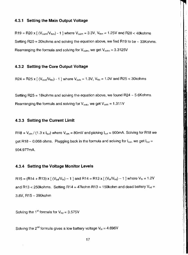
4.3.1 Setting the Main Output Voltage
R19 = R20 x [ (Vout,,,/Vfbm) - 1 ] where Voutm = 3.3V, Vfbm = 1.25V and R20 < 40kohms
Setting R20 = 20kohms and solving the equation above, we find R19 to be - 33Kohms.
Rearranging the formula and solving for Voutm, we get Voutm = 3.31 25V
4.3.2 Setting the Core Output Voltage
R24 = R25 x [ (VoutJVfbc) - 1 ] where Voutc = 1.3V, Vfbc = 1 .OV and R25 c 30kohms
Setting R25 = 18kohms and solving the equation above, we found R24 - 5.6Kohms.
Rearranging the formula and solving for Voutc, we get Voutc = 1.31 1V
4.3.3 Setting the Current Limit
R18 = VClm 1 (1.3 x lout) where VcIm = 80mV and picking lout = 900mA. Solving for R18 we
get R18 - 0.068 ohms. Plugging back in the formula and solving for lout, we get lout =
904.977mA.
4.3.4 Setting the Voltage Monitor Levels
R15 = (R14 + R13) x [ (VbdVth) - 1 ] and R14 = R13 x [ (Vbl/Vbd) - 1 ] where Vth = 1.2V
and R13 c 250kohms. Setting R14 = 47kohm R13 = 150kohm and dead battery VI,~ =
3.6V, R15 - 390kohm
Solving the 1 " formula for Vbd = 3.575V
Solving the 2nd formula gives a low battery voltage Vbl = 4.696V
17

(9V - 3.3V) x ( 400ns / 300 mA ) = 8.44uH. The closest value is 8.2uH.
4.3.6 Power Monitoring
The CPU power monitoring is done with two CPU voltage monitoring chips: the MAX81 1
and MAX81 2. When the CPU voltage drops below the 3.3V threshold, the PXA255 will
enter a sleep mode.
4.4 Flash ROM
The PXA255 is connected to four lntel 3V 256Mbit 28F256J3A StrataFlash memory
chips. A total of 128MB of flash memory is available accessible as 32bit words. Figure
4-3, JTAG wiring diagram taken from the lntel PXA255 Processor Design Guide, is used
for flash programming and debugging.
So a low battery and dead battery is defined when the voltage drops below 4.7V and
3.6V respectively.
4.3.5 Inductor Selection
30% of the 900mA maximum current load, = 300mA

Figure 4-3: JTAG Wiring Diagram
4.5 Synchronous Dynamic RAM
The PXA255 is connected to eight Samsung 256Mbit K4S561632B SDRAM chips. A
total of 256MB of SDRAM is accessible as 32bit words with two of the SDRAM chips
supplying 16bits.
4.6 Video Display
The PXA255 has a built in grey-scale, 8-bit and 16-bit color display modes for LCDs. To
convert the digital LCD outputs to an analog VGA signal, a Fairchild TMC3533 Triple
Video Digital-to-Analog Converter is used. The TMC3533 is available in 80, 50, and 30
megapixels per second. To support the maximum resolution of 1280x1 024 at 60Hz, we
would need a minimum bandwidth of 1280x1024~60 = 78643200 pixels per second.
Only the 80 megapixels per second version has sufficient bandwidth to handle required
maximum resolution.

4.7 RS-232 Port
The full function UART pins from the PXA255 connected to a MAX3243 will provide a
RS-232 serial port interface.

5 PCB and Layer Stack
The Printed Circuit Board (PCB) is made from Fire-Retardant 4 (FR-4) with '/2 ounce
copper plating. A yellow silkscreen was chosen with a green solder paste on top to
protect the board. A single sided board was not possible since the PXA255 and SA-
11 11 chips come in a 256 pin micro-ball gate array (mBGA) and the complexity of the
design. The only way to access all the embedded pins required a multi-layer board with
a structured fanout. The author used the following layer stack in Figure 5-1.
Top Layer
MidLayerl
InternalPlanel [GND]
InternalPlane2 (OC3.3V)
MidLayer2
Bottom Layer
Prepreg (1 2.6mil)
Core (1 2.6mil)
Prepreg [ I 2.6milI
Core [ I 2.6milI
Prepreg [ I 2.6mil)
Figure 5-1 : PCB Layer Stack

6 OPERATING SYSTEM
The designed system is capable of running both Windows CE and Linux. While Linux is
an open-source and Windows CE is a closed-source, the operating system chosen was
Windows CE for the following reasons. Windows CE is partially compatible with Win32
and is the platform of choice of many Pocket PCs and PDAs. The author is more
familiar with Windows than with Linux. In addition, Microsoft has provided free
development tools on their website making Windows CE easy decision.
7 CONCLUSION
The project has improved the skills and knowledge of the author tremendously and thus,
he believes the project as a success. The author was able to produce the desired end
product starting from a conceptual stage through to a manufacturing stage. However,
the path was not easy. The author spent a tremendous amount of time part sourcing,
planning and laying out the PCB. Mistakes in layout and even in schematics required
intensive checking and rechecking. In the end, the author has become very comfortable
and familiar with Protel, a PCB design and layout tool, and has experienced what is
required to bring a concept through to manufacturing. The author has also familiarized
himself of current manufacturing processes and capabilities. The experience, skills and
contacts made will be very beneficial for future work and increased the author's set of
skills.
7.1 Future Work
While the objective was to produce a functional prototype, the product needs more
refinement and improvement. Future work will include:
Increasing wireless range Improving efficiency and throughput Cost, size and weight reduction Bluetooth and USB support Tracking down and fixing bugs

APPENDIX
In this section, Figure 7-1 through Figure 7-9 are schematics while Figure 7-1 0 is
screenshot of the layout.

Figure 7-1 : PXA255 Schematic
25

Figure 7-2: Flash Schematic
26
Figure 7-3: SDRAM Schematic
27
Figure 7-4: SA-1111 Main Schematic

Figure 7-5: Video Schematic
29

Figure 7-6: SA-1111 PCMCIA Schematic

Figure 7-7: SA-1111 Keyboard & Mouse Schematic

Figure 7-8: RS-232 Schematic

Figure 7-9: Power Supply Schematic
33
Figure 7-1 0: PCB Layout
34

REFERENCES
Brian P. Crow, lndra Widjaja, Jeong Geun Kim, and Prescott Sakai, "Investigation of
the IEEE 802.1 1 Medium Access Control (MAC) Sublayer Functions", Proceedings
of IEEE INFOCOM, April 1997.
Dongyan Chen, Sachin Garg, Martin Kappes, and Kishor S. Trivedi, "Supporting
VBR VolP Traffic in IEEE 802.1 1 WLAN in PCF Mode", Proceedings of
OPNETWork 2002, Washington D.C., USA, August 2002.
IEEE 802.1 1 Working Group, "ANSI/IEEE Std. 802.1 1, 1999 Edition: Part 11 :
Wireless LAN Medium Access Control (MAC) and Physical Layer (PHY)
Specifications", 1999.
lntel Corporation, "lntel PXA255 Applications Processor's Developer's Manual", lntel
Corporation.
http://developer.intel.com/design/pca/applicationsprocessors/manuals/278693. htm.
Accessed: January 15,2004.
lntel Corporation, "lntel StrongARM SA-1111 Microprocessor Companion Chip
Developer's Manual", lntel Corporation.
http://developer.intel.com/design/strong/manuals/278242.htm.
Accessed: January 15,2004.
Maxim Semiconductors, "Dual, High-Efficiency, Step-Down Converter with Backup
Battery Switchover", Maxim Integrated Products.
http://www .maxim-ic.com/quick~view2.cfm/qv~pk/2375.
Accessed: January 15,2004.
Microsoft Developer Network, "VolP Industry Trends", Microsoft Windows
Embedded Developer Center.
http:Nmsdn.microsofi.com/embedded/devpla~oiptrends/default.aspx.
Accessed: January 15,2004.

[8] Sage Research, Inc., "Wireless LAN Adoption Trends 2004", January 2004.
http://www.researchandmarkets.com/reportinfo.asp?report~id=42791.
Accessed: January 15,2004.
[9] Stefan Mangold, Sunghyun Choi, Peter May, Ole Klein, Guido Hiertz, Lothar Stibor,
"IEEE 802.1 1 e Wireless LAN for Quality of Service", Proceedings of European
Wireless 2002, Florence, Italy, 2002.
[I 01 Stephen Casner and Van Jacobson, "Request for Comments 2508: Compressing
IPIUDPIRTP Headers for Low-Speed Serial Links", Internet Engineering Task
Force, February 1999.
[I 11 Zhenhua Xiao, Tejinder S. Randhawa, R.H. Stephen Hardy, "Performance Analysis
of CRTP in IEEE 802.1 1 Network, submitted to PlMRC February, 2004.