Embed Size (px)
Citation preview

Hardware
ELEC 330
Digital Systems Engineering
Dr. Ron Hayne

330_06 2
Hardware Building Blocks
Input/Output
ProcessorControl
Unit
Memory
ClockMicrocomputer/Microcontroller
Microprocessor

330_06 3
Memory
Memory Signals Address Bus
A15 - A0
Data Bus D7 - D0
Read/Write R/W
Timing Pulse CS Tri-state outputs
Mem
Address
Data
Read/Write
Timing Pulse

330_06 4
Hardware Terminology
Bus Collection of binary
signal wires
68HC11 Buses 16-bit Address Bus 8-bit Data Bus Control Bus
(Non) Volatile Memory No power - no data (No power - still data)
Read/Write memory Store/retrieve at full speed
Read Only Memory Store at much slower speed
Random Access Memory Equal time for all locations
Sequential Access Read/Write in order

330_06 5
Microprocessor Bus Connections
Microprocessor
RAM
I/O
EEPROM
ROM
ABUSDBUS

330_06 6
Bus Operation Example
Example Instruction (STAA) Register and Memory contents
PC
C100 B7 C1 00
C101 C2 IR
C102 00
A
22
B
C200 44 33
330_06 7
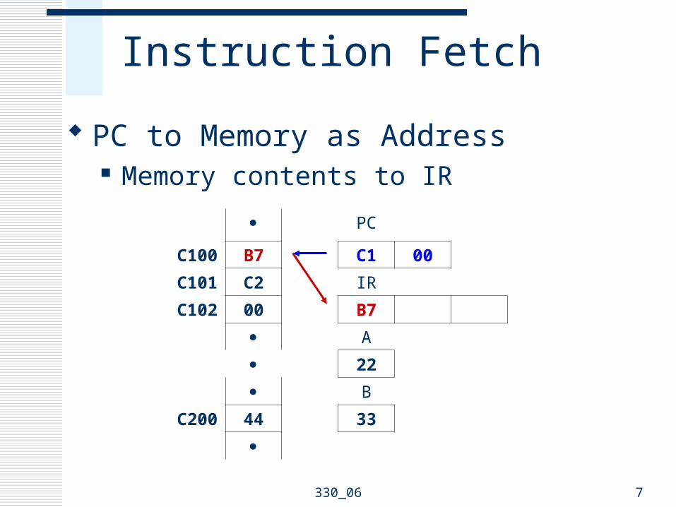
Instruction Fetch
PC to Memory as Address Memory contents to IR
PC
C100 B7 C1 00
C101 C2 IR
C102 00 B7
A
22
B
C200 44 33

330_06 8
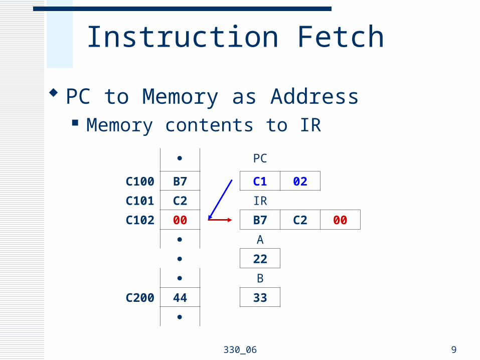
Instruction Fetch
PC to Memory as Address Memory contents to IR
PC
C100 B7 C1 01
C101 C2 IR
C102 00 B7 C2
A
22
B
C200 44 33
330_06 9
Instruction Fetch
PC to Memory as Address Memory contents to IR
PC
C100 B7 C1 02
C101 C2 IR
C102 00 B7 C2 00
A
22
B
C200 44 33

330_06 10
Instruction Execution
Operand Address to Memory Accumulator A contents to Memory
PC
C100 B7 C1 03
C101 C2 IR
C102 00 B6 C2 00
A
22
B
C200 22 33

330_06 11
Computer Failures
Grounded Address Bus Line Incorrect Address
Grounded Data Bus Line Incorrect Data
Intermittent Failures

330_06 12
Memory Mapping
68HC11A8 $0000-$00FF RAM $1000-$103F I/O $B600-$B7FF EEPROM $E000-$FFFF ROM
8 bits = 256 bytes 6 bits = 64 bytes 9 bits = 512 bytes 13 bits = 8K bytes
15 14 13 12 11 10 9 8 7 6 5 4 3 2 1 0
RAM 0 0 0 0 0 0 0 0 X X X X X X X X
I/O 0 0 0 1 0 0 0 0 0 0 X X X X X X
EEPROM 1 0 1 1 0 1 1 X X X X X X X X X
ROM 1 1 1 X X X X X X X X X X X X X

330_06 13
Creating a Memory Map
Resources 2K bytes RAM 128 bytes I/O 4K bytes EEPROM 32K bytes ROM
11 bits 7 bits 12 bits 15 bits
15 14 13 12 11 10 9 8 7 6 5 4 3 2 1 0
RAM
I/O
EEPROM
ROM

330_06 14
Creating a Memory Map
Resources 2K bytes RAM 128 bytes I/O 4K bytes EEPROM 32K bytes ROM
11 bits 7 bits 12 bits 15 bits
15 14 13 12 11 10 9 8 7 6 5 4 3 2 1 0
RAM 0 0 0 0 0 X X X X X X X X X X X
I/O
EEPROM
ROM
$0000-$07FF

330_06 15
Creating a Memory Map
Resources 2K bytes RAM 128 bytes I/O 4K bytes EEPROM 32K bytes ROM
11 bits 7 bits 12 bits 15 bits
15 14 13 12 11 10 9 8 7 6 5 4 3 2 1 0
RAM 0 0 0 0 0 X X X X X X X X X X X
I/O
EEPROM
ROM 1 X X X X X X X X X X X X X X X
$0000-$07FF
$8000-$FFFF

330_06 16
Creating a Memory Map
Resources 2K bytes RAM 128 bytes I/O 4K bytes EEPROM 32K bytes ROM
11 bits 7 bits 12 bits 15 bits
15 14 13 12 11 10 9 8 7 6 5 4 3 2 1 0
RAM 0 0 0 0 0 X X X X X X X X X X X
I/O 0 0 0 1 0 0 0 0 0 X X X X X X X
EEPROM
ROM 1 X X X X X X X X X X X X X X X
$0000-$07FF $1000-$107F
$8000-$FFFF

330_06 17
Creating a Memory Map
Resources 2K bytes RAM 128 bytes I/O 4K bytes EEPROM 32K bytes ROM
11 bits 7 bits 12 bits 15 bits
15 14 13 12 11 10 9 8 7 6 5 4 3 2 1 0
RAM 0 0 0 0 0 X X X X X X X X X X X
I/O 0 0 0 1 0 0 0 0 0 X X X X X X X
EEPROM 0 0 1 1 X X X X X X X X X X X X
ROM 1 X X X X X X X X X X X X X X X
$0000-$07FF $1000-$107F $3000-$3FFF $8000-$FFFF

330_06 18
Parallel I/O
I/O Programming Model Data Transfer
Input Port LDAA
Output Port STAA
Synchronization (Timing)Flag
I/O device ready
Polling Repeatedly tests I/O flags

330_06 19
Memory Map
THRSim11 $0000-$00FF RAM $1000-$103F I/O $B600-$B7FF RAM $E000-$FFFF ROM
8 bits = 256 bytes 6 bits = 64 bytes 9 bits = 512 bytes 13 bits = 8K bytes
15 14 13 12 11 10 9 8 7 6 5 4 3 2 1 0
RAM 0 0 0 0 0 0 0 0 X X X X X X X X
I/O 0 0 0 1 0 0 0 0 0 0 X X X X X X
RAM 1 0 1 1 0 1 1 X X X X X X X X X
ROM 1 1 1 X X X X X X X X X X X X X

330_06 20
I/O Registers
Memory-Mapped I/O
Name Address Function
PORTA $1000 Timer and Counter System
PORTB $1004 Parallel Output
PORTC $1003 Parallel Input/Output
PORTCL $1005 PORTC Latch
PORTD $1008 Serial Input/Output
PORTE $100A Analog-to-Digital Converters
PIOC $1002 Parallel I/O Control
DDRC $1007 Data Direction PORTC
DDRD $1009 Data Direction PORTD

330_06 21
Parallel I/O Hardware
Output Port PORTB $1004
Input Port PORTC $1003

330_06 22
Logical Operations
Bit Set and Clear BSET
Set all bits in a memorybyte that correspond to 1sin the mask
BCLR Clear all bits in a memory
byte that correspond tothe 1s in the mask
Assembly Language BSET LIGHTS,%00010000
Bit Testing and Branching BRSET
Branch if all the bits in a memory byte that correspond to 1s in the mask are set
BRCLR Branch if all the bits in a
memory byte that correspond to 1s in the mask are clear
Assembly Language BRCLR 0,X,MASK1,NEXT

330_06 23
Programming Example
Light PB5 if PC6 = 1 AND PC2 = 0

330_06 24
Programming Example
** Symbol Definitions
PORTC EQU $1003
PORTB EQU $1004
BIT2 EQU %00000100
BIT5 EQU %00100000
BIT6 EQU %01000000
** Data Section
ORG $10
IMAGE FCB $00 Copy of Output Bits
** Program Section Goes Here.....
* Reset Vector
ORG $FFFE
FDB LOOP
END

330_06 25
Programming Example** Program Section
ORG $E100
* Test Input Switches
LOOP LDX #PORTC
BRCLR 0,X,BIT6,NEXT Test Bit-6
BRSET 0,X,BIT2,NEXT Test Bit-2
* Set IMAGE Bit-5
BSET IMAGE,BIT5
BRA OUT
* Clear IMAGE Bit-5
NEXT BCLR IMAGE,BIT5
* Output to Port
OUT LDAA IMAGE
STAA PORTB
BRA LOOP

330_06 26
Parallel I/O Hardware
DDRC Register Data Direction Register
0 input bit 1 output bit
PIOC Register Parallel I/O Control Register
STAF Flag Bit (7) STRA Strobe A pin
PORTCL PORTC Latch Controlled by STRA pin

330_06 27
Polling Software
Loop to Test STAF (STRA)PBTST TST PIOC
BPL PBTST
Read PORTCL and Clear STAF LDAA PIOC
LDAA PORTCL
Manipulate Data ...

330_06 28
Interrupt System
Main Program in Infinite Loop When I/O Ready, Sets I/O Flag Hardware Interrupt System Responds
Stops Main Program Saves Status
Transfers to Interrupt Service Routine Clears I/O Flag Transfers Data Returns
Main Program Resumes Restores Status

330_06 29
Interrupt Hardware
Interrupt Request Line (IRQ) Active Low Condition Code (I bit) Enables Interrupts
Active Low CLI
I/O Flag Enable Interrupt
Stack Status (info in registers) saved Status restored on RTI
Interrupt Vectors Addresses of Interrupt Service Routines (ISR)

330_06 30
IRQ Example
Using STAF flag to cause interrupts STAI Interrupt Enable (1 = enable) EGA Edge for STRA (1 = low-to-high)
7 6 5 4 3 2 1 0
$1002 STAF STAI EGA PIOC

330_06 31
Interrupt Program
Interrupt Vector ORG $FFF2
FDB IRQISR
Initialize Stack LDS #$B7FF
Set Up PIOC LDAA #%01000010
STAA PIOC
Enable Interrupts CLI
Wait for InterruptsHERE BRA HERE
330_06 32
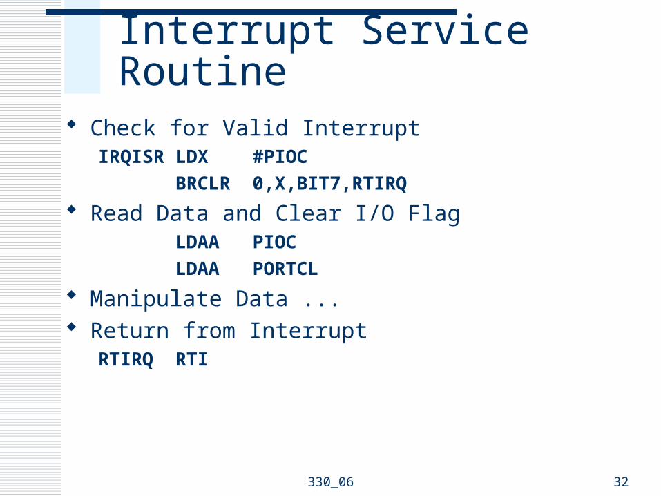
Interrupt Service Routine
Check for Valid InterruptIRQISR LDX #PIOC
BRCLR 0,X,BIT7,RTIRQ
Read Data and Clear I/O Flag LDAA PIOC
LDAA PORTCL
Manipulate Data ... Return from Interrupt
RTIRQ RTI

330_06 33
Interrupt Issues
Multiple Interrupt Sources Poll flags to determine source
Interrupting an ISR Service only one interrupt at a time Queue based on priority
Concurrency Problem Different parts of program accessing common resources
Reentrancy Problem Subroutine reentered due to interrupt

330_06 34
Summary
Memory Buses Memory Mapping Parallel I/O Interrupts