Embed Size (px)
Citation preview

Intel® Quark SoC X1000 CoreHardware Reference Manual
October 2013
Order Number: 329678-001US

Intel® Quark SoC X1000 CoreHardware Reference Manual October 20132 Order Number: 329678-001US
Legal Lines and DisclaimersINFORMATION IN THIS DOCUMENT IS PROVIDED IN CONNECTION WITH INTEL PRODUCTS. NO LICENSE, EXPRESS OR IMPLIED, BY ESTOPPEL OR OTHERWISE, TO ANY INTELLECTUAL PROPERTY RIGHTS IS GRANTED BY THIS DOCUMENT. EXCEPT AS PROVIDED IN INTEL'S TERMS AND CONDITIONS OF SALE FOR SUCH PRODUCTS, INTEL ASSUMES NO LIABILITY WHATSOEVER AND INTEL DISCLAIMS ANY EXPRESS OR IMPLIED WARRANTY, RELATING TO SALE AND/OR USE OF INTEL PRODUCTS INCLUDING LIABILITY OR WARRANTIES RELATING TO FITNESS FOR A PARTICULAR PURPOSE, MERCHANTABILITY, OR INFRINGEMENT OF ANY PATENT, COPYRIGHT OR OTHER INTELLECTUAL PROPERTY RIGHT.A "Mission Critical Application" is any application in which failure of the Intel Product could result, directly or indirectly, in personal injury or death. SHOULD YOU PURCHASE OR USE INTEL'S PRODUCTS FOR ANY SUCH MISSION CRITICAL APPLICATION, YOU SHALL INDEMNIFY AND HOLD INTEL AND ITS SUBSIDIARIES, SUBCONTRACTORS AND AFFILIATES, AND THE DIRECTORS, OFFICERS, AND EMPLOYEES OF EACH, HARMLESS AGAINST ALL CLAIMS COSTS, DAMAGES, AND EXPENSES AND REASONABLE ATTORNEYS' FEES ARISING OUT OF, DIRECTLY OR INDIRECTLY, ANY CLAIM OF PRODUCT LIABILITY, PERSONAL INJURY, OR DEATH ARISING IN ANY WAY OUT OF SUCH MISSION CRITICAL APPLICATION, WHETHER OR NOT INTEL OR ITS SUBCONTRACTOR WAS NEGLIGENT IN THE DESIGN, MANUFACTURE, OR WARNING OF THE INTEL PRODUCT OR ANY OF ITS PARTS.Intel may make changes to specifications and product descriptions at any time, without notice. Designers must not rely on the absence or characteristics of any features or instructions marked "reserved" or "undefined". Intel reserves these for future definition and shall have no responsibility whatsoever for conflicts or incompatibilities arising from future changes to them. The information here is subject to change without notice. Do not finalize a design with this information.The products described in this document may contain design defects or errors known as errata which may cause the product to deviate from published specifications. Current characterized errata are available on request.Contact your local Intel sales office or your distributor to obtain the latest specifications and before placing your product order.Copies of documents which have an order number and are referenced in this document, or other Intel literature, may be obtained by calling 1-800-548-4725, or go to: http://www.intel.com/design/literature.htm Any software source code reprinted in this document is furnished for informational purposes only and may only be used or copied and no license, express or implied, by estoppel or otherwise, to any of the reprinted source code is granted by this document.Intel processor numbers are not a measure of performance. Processor numbers differentiate features within each processor family, not across different processor families. Go to: http://www.intel.com/products/processor_number/Code Names are only for use by Intel to identify products, platforms, programs, services, etc. (“products”) in development by Intel that have not been made commercially available to the public, i.e., announced, launched or shipped. They are never to be used as “commercial” names for products. Also, they are not intended to function as trademarks.Intel and the Intel logo are trademarks of Intel Corporation in the U.S. and/or other countries.*Other names and brands may be claimed as the property of others.Copyright © 2013, Intel Corporation. All rights reserved.
Revision History—Intel® Quark Core
Revision History
Date Revision Description
September 2013 001 First external release of document.
Intel® Quark SoC X1000 CoreOctober 2013 Hardware Reference ManualOrder Number: 329678-001US 3

Intel® Quark Core—Contents
Contents
1.0 About this Manual ....................................................................................................101.1 Manual Contents................................................................................................101.2 Notational Conventions.......................................................................................111.3 Special Terminology...........................................................................................121.4 Related Documents ............................................................................................12
2.0 Introduction ............................................................................................................132.1 Intel® Quark Core Features.................................................................................132.2 Intel® Quark Core Product ..................................................................................15
2.2.1 Operating Modes and Compatibility ...........................................................152.2.2 Memory Management..............................................................................152.2.3 On-chip Cache........................................................................................152.2.4 Floating-Point Unit ..................................................................................16
2.3 System Components ..........................................................................................162.4 System Architecture...........................................................................................162.5 Systems Applications .........................................................................................17
2.5.1 Embedded Personal Computers.................................................................172.5.2 Embedded Controllers .............................................................................18
3.0 Internal Architecture ...............................................................................................193.1 Instruction Pipelining..........................................................................................223.2 Bus Interface Unit..............................................................................................22
3.2.1 Data Transfers .......................................................................................233.2.2 Write Buffers..........................................................................................233.2.3 Locked Cycles ........................................................................................243.2.4 I/O Transfers .........................................................................................24
3.3 Cache Unit ........................................................................................................253.3.1 Cache Structure .....................................................................................253.3.2 Cache Updating ......................................................................................263.3.3 Cache Replacement.................................................................................273.3.4 Cache Configuration................................................................................27
3.4 Instruction Prefetch Unit .....................................................................................283.5 Instruction Decode Unit ......................................................................................283.6 Control Unit ......................................................................................................293.7 Integer (Datapath) Unit ......................................................................................293.8 Floating-Point Unit .............................................................................................29
3.8.1 Intel® Quark Core Floating-Point Unit ........................................................293.9 Segmentation Unit .............................................................................................293.10 Paging Unit .......................................................................................................30
4.0 Bus Operation ..........................................................................................................324.1 Data Transfer Mechanism ...................................................................................32
4.1.1 Memory and I/O Spaces ..........................................................................324.1.1.1 Memory and I/O Space Organization............................................33
4.1.2 Dynamic Data Bus Sizing .........................................................................344.1.3 Interfacing with 8-, 16-, and 32-Bit Memories.............................................354.1.4 Dynamic Bus Sizing During Cache Line Fills ................................................394.1.5 Operand Alignment .................................................................................40
4.2 Bus Arbitration Logic ..........................................................................................414.3 Bus Functional Description ..................................................................................44
4.3.1 Non-Cacheable Non-Burst Single Cycle ......................................................444.3.1.1 No Wait States..........................................................................444.3.1.2 Inserting Wait States .................................................................45
Intel® Quark SoC X1000 CoreHardware Reference Manual October 20134 Order Number: 329678-001US

Contents—Intel® Quark Core
4.3.2 Multiple and Burst Cycle Bus Transfers ...................................................... 464.3.2.1 Burst Cycles............................................................................. 464.3.2.2 Terminating Multiple and Burst Cycle Transfers ............................. 474.3.2.3 Non-Cacheable, Non-Burst, Multiple Cycle Transfers ...................... 484.3.2.4 Non-Cacheable Burst Cycles ....................................................... 48
4.3.3 Cacheable Cycles ................................................................................... 494.3.3.1 Byte Enables during a Cache Line Fill ........................................... 504.3.3.2 Non-Burst Cacheable Cycles ....................................................... 514.3.3.3 Burst Cacheable Cycles.............................................................. 524.3.3.4 Effect of Changing KEN# during a Cache Line Fill .......................... 53
4.3.4 Burst Mode Details ................................................................................. 534.3.4.1 Adding Wait States to Burst Cycles.............................................. 534.3.4.2 Burst and Cache Line Fill Order ................................................... 554.3.4.3 Interrupted Burst Cycles ............................................................ 56
4.3.5 8- and 16-Bit Cycles ............................................................................... 574.3.6 Locked Cycles ........................................................................................ 594.3.7 Pseudo-Locked Cycles............................................................................. 60
4.3.7.1 Floating-Point Read and Write Cycles........................................... 614.3.8 Invalidate Cycles.................................................................................... 61
4.3.8.1 Rate of Invalidate Cycles ........................................................... 634.3.8.2 Running Invalidate Cycles Concurrently with Line Fills.................... 63
4.3.9 Bus Hold ............................................................................................... 664.3.10 Interrupt Acknowledge............................................................................ 674.3.11 Special Bus Cycles.................................................................................. 68
4.3.11.1 HALT Indication Cycle................................................................ 684.3.11.2 Shutdown Indication Cycle ......................................................... 694.3.11.3 Stop Grant Indication Cycle........................................................ 69
4.3.12 Bus Cycle Restart ................................................................................... 704.3.13 Bus States............................................................................................. 724.3.14 Floating-Point Error Handling for Intel® Quark Core .................................... 73
4.3.14.1 Floating-Point Exceptions ........................................................... 734.3.15 Intel® Quark Core Floating-Point Error Handling in AT-Compatible Systems.... 74
4.4 Enhanced Bus Mode Operation (Write-Back Mode) ................................................. 744.4.1 Summary of Bus Differences.................................................................... 744.4.2 Burst Cycles .......................................................................................... 74
4.4.2.1 Non-Cacheable Burst Operation .................................................. 754.4.2.2 Burst Cycle Signal Protocol......................................................... 75
4.4.3 Cache Consistency Cycles........................................................................ 764.4.3.1 Snoop Collision with a Current Cache Line Operation ..................... 774.4.3.2 Snoop under AHOLD.................................................................. 784.4.3.3 Snoop During Replacement Write-Back ........................................ 804.4.3.4 Snoop under BOFF#.................................................................. 824.4.3.5 Snoop under HOLD ................................................................... 844.4.3.6 Snoop under HOLD during Replacement Write-Back....................... 86
4.4.4 Locked Cycles ........................................................................................ 864.4.4.1 Snoop/Lock Collision ................................................................. 88
4.4.5 Flush Operation...................................................................................... 884.4.6 Pseudo Locked Cycles ............................................................................. 89
4.4.6.1 Snoop under AHOLD during Pseudo-Locked Cycles ........................ 894.4.6.2 Snoop under Hold during Pseudo-Locked Cycles............................ 904.4.6.3 Snoop under BOFF# Overlaying a Pseudo-Locked Cycle ................. 91
5.0 Memory Subsystem Design ...................................................................................... 935.1 Introduction ..................................................................................................... 935.2 Processor and Cache Feature Overview ................................................................ 93
5.2.1 The Burst Cycle...................................................................................... 935.2.2 The KEN# Input ..................................................................................... 94
Intel® Quark SoC X1000 CoreOctober 2013 Hardware Reference ManualOrder Number: 329678-001US 5

Intel® Quark Core—Contents
6.0 Cache Subsystem .....................................................................................................976.1 Introduction......................................................................................................976.2 Cache Memory ..................................................................................................97
6.2.1 What is a Cache? ....................................................................................976.3 Cache Trade-offs ...............................................................................................98
6.3.1 Intel® Quark Core Cache Organization.......................................................986.3.2 Block/Line Size.......................................................................................996.3.3 Replacement Policy ...............................................................................100
6.4 Updating Main Memory .....................................................................................1006.4.1 Write-Through and Buffered Write-Through Systems .................................1006.4.2 Write-Back System ...............................................................................1016.4.3 Cache Consistency ................................................................................101
6.5 Non-Cacheable Memory Locations ......................................................................1036.6 Cache and DMA Operations ...............................................................................103
7.0 Peripheral Subsystem ............................................................................................1057.1 Peripheral/Processor Bus Interface .....................................................................105
7.1.1 Mapping Techniques..............................................................................1057.1.2 Dynamic Data Bus Sizing .......................................................................1077.1.3 Address Decoding for I/O Devices ...........................................................108
7.1.3.1 Address Bus Interface..............................................................1097.1.3.2 32-Bit I/O Interface.................................................................109
7.2 Basic Peripheral Subsystem...............................................................................1117.2.1 Bus Control and Ready Logic ..................................................................1137.2.2 Bus Control Signal Description................................................................114
7.2.2.1 Intel® Quark Core Interface......................................................1147.2.3 Wait State Generator Logic ....................................................................1157.2.4 Address Decoder ..................................................................................1167.2.5 Recovery and Bus Contention .................................................................1197.2.6 Write Buffers and I/O Cycles ..................................................................119
7.2.6.1 Write Buffers and Recovery Time...............................................1197.2.7 Non-Cacheability of Memory-Mapped I/O Devices......................................1207.2.8 Intel® Quark Core On-Chip Cache Consistency..........................................120
7.3 I/O Cycles ......................................................................................................1207.3.1 Read Cycle Timing ................................................................................1207.3.2 Write Cycle Timings ..............................................................................122
8.0 Local APIC .............................................................................................................1258.1 Local APIC Overview ........................................................................................1258.2 LAPIC Register Structure ..................................................................................126
8.2.1 APIC Timer ..........................................................................................1308.2.2 Interrupt Control Register (ICR), Logical Destination Register (LDR),
Destination Format Register (DFR) ..........................................................1318.2.3 Interrupt and Task Priority .....................................................................1318.2.4 Fixed Interrupts....................................................................................1318.2.5 End of Interrupt (EOI) ...........................................................................132
9.0 Clocking Considerations and System Debugging ....................................................1339.1 Clocking Considerations....................................................................................133
9.1.1 Intel® Quark Core Clocking Architectures.................................................1339.1.1.1 Two Phase Flop Design.............................................................1339.1.1.2 LMT Single Phase Flop Design ...................................................1349.1.1.3 Intel® Quark Core 1-clock Flop Design .......................................135
9.1.2 SoC / Intel® Quark Core Clock Architecture..............................................1359.1.3 Intel® Quark Core Core/Bus/SoC Clock Ratio............................................1369.1.4 Clock Skew and Uncertainty ...................................................................137
Intel® Quark SoC X1000 CoreHardware Reference Manual October 20136 Order Number: 329678-001US

Contents—Intel® Quark Core
9.1.4.1 Clock Uncertainty Components and Numbers .............................. 1379.2 Building and Debugging a Intel® Quark Core-Based System.................................. 138
9.2.1 Debugging Features of the Intel® Quark Core .......................................... 1409.2.2 Breakpoint Instruction .......................................................................... 1409.2.3 Single-Step Trap .................................................................................. 1409.2.4 Debug Registers................................................................................... 1409.2.5 Debug Control Register (DR7) ................................................................ 1429.2.6 Debugging Overview............................................................................. 143
Figures1 Intel® Quark SoC X1000 Core used in Intel® Quark SoC X1000................................... 172 Embedded Personal Computer and Embedded Controller Example................................ 183 Intel® Quark Core Block Diagram ............................................................................ 204 Internal Pipelining ................................................................................................. 225 Intel® Quark SoC X1000 Core Cache Organization ..................................................... 266 Segmentation and Paging Address Formats............................................................... 307 Translation Lookaside Buffer ................................................................................... 318 Physical Memory and I/O Spaces ............................................................................. 339 Physical Memory and I/O Space Organization............................................................ 3410 Intel® Quark Core with 32-Bit Memory..................................................................... 3611 Addressing 16- and 8-Bit Memories ......................................................................... 3612 Logic to Generate A1, BHE# and BLE# for 16-Bit Buses.............................................. 3813 Data Bus Interface to 16- and 8-Bit Memories ........................................................... 3914 Single Master Intel® Quark Core System .................................................................. 4115 Single Master Intel® Quark Core with DMA ............................................................... 4216 Single Master Intel® Quark Core with Multiple Secondary Masters................................ 4317 Basic 2-2 Bus Cycle ............................................................................................... 4518 Basic 3-3 Bus Cycle ............................................................................................... 4619 Non-Cacheable, Non-Burst, Multiple-Cycle Transfers .................................................. 4820 Non-Cacheable Burst Cycle..................................................................................... 4921 Non-Burst, Cacheable Cycles .................................................................................. 5122 Burst Cacheable Cycle............................................................................................ 5223 Effect of Changing KEN# ........................................................................................ 5324 Slow Burst Cycle ................................................................................................... 5425 Burst Cycle Showing Order of Addresses................................................................... 5526 Interrupted Burst Cycle.......................................................................................... 5627 Interrupted Burst Cycle with Non-Obvious Order of Addresses..................................... 5728 8-Bit Bus Size Cycle............................................................................................... 5829 Burst Write as a Result of BS8# or BS16#................................................................ 5930 Locked Bus Cycle .................................................................................................. 6031 Pseudo Lock Timing ............................................................................................... 6132 Fast Internal Cache Invalidation Cycle...................................................................... 6233 Typical Internal Cache Invalidation Cycle .................................................................. 6234 System with Second-Level Cache ............................................................................ 6435 Cache Invalidation Cycle Concurrent with Line Fill ...................................................... 6536 HOLD/HLDA Cycles................................................................................................ 6637 HOLD Request Acknowledged during BOFF# ............................................................. 6738 Interrupt Acknowledge Cycles ................................................................................. 6839 Stop Grant Bus Cycle ............................................................................................. 6940 Restarted Read Cycle............................................................................................. 7041 Restarted Write Cycle ............................................................................................ 7142 Bus State Diagram ................................................................................................ 7243 Basic Burst Read Cycle........................................................................................... 75
Intel® Quark SoC X1000 CoreOctober 2013 Hardware Reference ManualOrder Number: 329678-001US 7

Intel® Quark Core—Contents
44 Snoop Cycle Overlaying a Line-Fill Cycle ...................................................................7945 Snoop Cycle Overlaying a Non-Burst Cycle ................................................................8046 Snoop to the Line that is Being Replaced...................................................................8147 Snoop under BOFF# during a Cache Line-Fill Cycle .....................................................8348 Snoop under BOFF# to the Line that is Being Replaced ...............................................8449 Snoop under HOLD during Cache Line Fill..................................................................8550 Snoop using HOLD during a Non-Cacheable, Non-Burstable Code Prefetch.....................8651 Locked Cycles (Back-to-Back) .................................................................................8752 Snoop Cycle Overlaying a Locked Cycle ....................................................................8853 Flush Cycle ...........................................................................................................8954 Snoop under AHOLD Overlaying Pseudo-Locked Cycle.................................................9055 Snoop under HOLD Overlaying Pseudo-Locked Cycle ..................................................9156 Snoop under BOFF# Overlaying a Pseudo-Locked Cycle ..............................................9257 Typical Burst Cycle.................................................................................................9558 Burst Cycle: KEN# Normally Active ..........................................................................9659 Cache Data Organization for the Intel® Quark Core On-Chip Cache ..............................9960 Bus Watching/Snooping for Shared Memory Systems ...............................................10261 Hardware Transparency........................................................................................10262 Non-Cacheable Share Memory...............................................................................10363 Mapping Scheme .................................................................................................10664 Intel® Quark Core Interface to I/O Devices .............................................................10965 32-Bit I/O Interface .............................................................................................11066 System Block Diagram .........................................................................................11267 Basic I/O Interface Block Diagram..........................................................................11368 PLD Equations for Basic I/O Control Logic ...............................................................11669 I/O Address Example ...........................................................................................11770 Internal Logic and Truth Table of 74S138................................................................11871 I/O Read Timing Analysis......................................................................................12172 I/O Read Timings.................................................................................................12173 I/O Write Cycle Timings........................................................................................12274 I/O Write Cycle Timing Analysis .............................................................................12375 Posted Write Circuit .............................................................................................12376 Timing of a Posted Write.......................................................................................12477 LAPIC Diagram....................................................................................................12578 Two phase flop based Intel® Quark Core design.......................................................13379 Clock waveforms for a two phase clock design .........................................................13480 Single phase flop based Intel® Quark Core design....................................................13481 Clock Waveforms for Single Phase flop based Intel® Quark Core design ......................13482 Intel® Quark Core 1-Clock Flop Based Design..........................................................13583 Intel® Quark Core Clocking Architecture Block Diagram for two-phase clock ................13584 Intel® Quark Core Clocking Architecture Block Diagram for single-phase clock .............13685 Intel® Quark Core Clocking Architecture Block Diagram for 1-clock design...................13686 Intel® Quark Core Clock Zones..............................................................................13787 Intel® Quark SoC X1000 Core used in Intel® Quark SoC X1000 .................................13988 Debug Registers ..................................................................................................141
Tables1 Intel® Quark Core Functional Units ..........................................................................192 Cache Configuration Options ...................................................................................273 Byte Enables and Associated Data and Operand Bytes ................................................324 Generating A31–A0 from BE3#–BE0# and A31–A2.....................................................335 Next Byte Enable Values for BSx# Cycles..................................................................356 Data Pins Read with Different Bus Sizes....................................................................357 Generating A1, BHE# and BLE# for Addressing 16-Bit Devices.....................................37
Intel® Quark SoC X1000 CoreHardware Reference Manual October 20138 Order Number: 329678-001US

Contents—Intel® Quark Core
8 Generating A0, A1 and BHE# from the Intel® Quark Core Byte Enables ........................ 399 Transfer Bus Cycles for Bytes, Words and Dwords...................................................... 4010 Burst Order (Both Read and Write Bursts) ................................................................ 5511 Special Bus Cycle Encoding..................................................................................... 6912 Bus State Description ............................................................................................ 7213 Snoop Cycles under AHOLD, BOFF#, or HOLD ........................................................... 7614 Various Scenarios of a Snoop Write-Back Cycle Colliding with an On-Going
Cache Fill or Replacement Cycle .............................................................................. 7715 Access Length of Typical CPU Functions.................................................................... 9416 Next Byte-Enable Values for the BSx# Cycles.......................................................... 10717 Valid Data Lines for Valid Byte Enable Combinations ................................................ 10818 32-Bit to 32-Bit Bus Swapping Logic Truth Table ..................................................... 11019 Bus Cycle Definitions ........................................................................................... 11420 LAPIC Register Address Map and Fields .................................................................. 12621 Intel® Quark Core Supported Clock Ratios .............................................................. 13722 Intel® Quark Core Clock Uncertainty Numbers ........................................................ 13823 LENi Fields ......................................................................................................... 142
§ §
Intel® Quark SoC X1000 CoreOctober 2013 Hardware Reference ManualOrder Number: 329678-001US 9

Intel® Quark Core—About this Manual
1.0 About this Manual
This manual describes the embedded Intel® Quark Core. It is intended for use by hardware designers familiar with the principles of embedded microprocessors and with the Intel® Quark Core architecture.
1.1 Manual ContentsThis section summarizes the contents of the chapters in this manual. The remainder of this chapter describes conventions and special terminology used throughout the manual and provides references to related documentation.
Chapter Description
Chapter 2.0, “Introduction”
This chapter provides an overview of the embedded Intel® Quark Core, including product features, system components, system architecture, and applications. This chapter also lists product frequency, voltage and package offerings.
Chapter 3.0, “Internal Architecture”
This chapter describes the Intel® Quark Core internal architecture, with a description of the processor’s functional units.
Chapter 4.0, “Bus Operation”
This chapter describes the features of the Intel® Quark Core bus, including bus cycle handling, interrupt and reset signals, cache control, and floating-point error control.
Chapter 5.0, “Memory Subsystem Design”
This chapter designing a memory subsystem that supports features of the Intel® Quark Core such as burst cycles and cache. This chapter also discusses using write-posting and interleaving to reduce bus cycle latency.
Chapter 6.0, “Cache Subsystem”
This chapter discusses cache theory and the impact of caches on performance. This chapter details different cache configurations, including direct-mapped, set associative, and fully associative. In addition, write-back and write-through methods for updating main memory are described.
Chapter 7.0, “Peripheral Subsystem”
This chapter describes the connection of peripheral devices to the Intel® Quark Core bus. Design techniques are discussed for interfacing a variety of devices, including a LAN controller and an interrupt controller.
Chapter 8.0, “Local APIC”
This chapter lists Local APIC (advanced programmable interrupt controller) registers. The local APIC (LAPIC) receives interrupts from the processor’s interrupt pins, from internal sources, and SoC and sends these to the CPU for handling the interrupts. The LAPIC currently does not support sending/receiving inter processor interrupt (IPI) messages to and from other processors on the system bus. The local APIC consists of a set of APIC registers and associated hardware that control the delivery of interrupts to the processor core.
Chapter 9.0, “Clocking Considerations and System Debugging”
This chapter describes clocking design guidelines and system debugging issues.
Intel® Quark SoC X1000 CoreHardware Reference Manual October 201310 Order Number: 329678-001US

About this Manual—Intel® Quark Core
1.2 Notational ConventionsThe following notations are used throughout this manual.
# The pound symbol (#) appended to a signal name indicates that the signal is active low.
Variables Variables are shown in italics. Variables must be replaced with correct values.
New Terms New terms are shown in italics. See the Glossary for a brief definition of commonly used terms.
Instructions Instruction mnemonics are shown in uppercase. When you are programming, instructions are not case-sensitive. You may use either upper- or lowercase.
Numbers Hexadecimal numbers are represented by a string of hexadecimal digits followed by the character H. A zero prefix is added to numbers that begin with A through F. (For example, FF is shown as 0FFH.) Decimal and binary numbers are represented by their customary notations. (That is, 255 is a decimal number and 1111 1111 is a binary number. In some cases, the letter B is added for clarity.)
Units of Measure The following abbreviations are used to represent units of measure:
Register Bits When the text refers to more that one bit, the range of bits is represented by the highest and lowest numbered bits, separated by a long dash (example: A15–A8). The first bit shown (15 in the example) is the most-significant bit and the second bit shown (8) is the least-significant bit.
A amps, amperesGbyte gigabytesKbyte kilobytesKΩ kilo-ohmsmA milliamps, milliamperesMbyte megabytesMHz megahertzms millisecondsmW milliwattsns nanosecondspF picofaradsW wattsV voltsμA microamps,
microamperesμF microfaradsμs microsecondsμW microwatts
Intel® Quark SoC X1000 CoreOctober 2013 Hardware Reference ManualOrder Number: 329678-001US 11
Intel® Quark Core—About this Manual
Register Names Register names are shown in uppercase. If a register name contains a lowercase italic character, it represents more than one register. For example, PnCFG represents three registers: P1CFG, P2CFG, and P3CFG.
Signal Names Signal names are shown in uppercase. When several signals share a common name, an individual signal is represented by the signal name followed by a number, while the group is represented by the signal name followed by a variable (n). For example, the lower chip-select signals are named CS0#, CS1#, CS2#, and so on; they are collectively called CSn#. A pound symbol (#) appended to a signal name identifies an active-low signal. Port pins are represented by the port abbreviation, a period, and the pin number (e.g., P1.0, P1.1).
1.3 Special TerminologyThe following terms have special meanings in this manual.
Assert and Deassert The terms assert and deassert refer to the acts of making a signal active and inactive, respectively. The active polarity (high/low) is defined by the signal name. Active-low signals are designated by the pound symbol (#) suffix; active-high signals have no suffix. To assert RD# is to drive it low; to assert HOLD is to drive it high; to deassert RD# is to drive it high; to deassert HOLD is to drive it low.
DOS I/O Address Peripherals that are compatible with PC/AT system architecture can be mapped into DOS (or PC/AT) addresses 0H–03FFH. In this manual, the terms DOS address and PC/AT address are synonymous.
Expanded I/O Address All peripheral registers reside at I/O addresses 0F000H–0FFFFH. PC/AT-compatible integrated peripherals can also be mapped into DOS (or PC/AT) address space (0H–03FFH).
PC/AT Address Integrated peripherals that are compatible with PC/AT system architecture can be mapped into PC/AT (or DOS) addresses 0H–03FFH. In this manual, the terms DOS address and PC/AT address are synonymous.
Set and Clear The terms set and clear refer to the value of a bit or the act of giving it a value. If a bit is set, its value is “1”; setting a bit gives it a “1” value. If a bit is clear, its value is “0”; clearing a bit gives it a “0” value.
1.4 Related DocumentsThe following Intel documents contain additional information on designing systems that incorporate the Intel® Quark Core.
Document Name Number
Intel® Quark SoC X1000 Core Developer’s Manual 329679
Intel® 64 and IA-32 Architectures Software Developer’s ManualCombined Volumes: 1, 2A, 2B, 2C, 3A, 3B and 3C
325462
Intel® Quark SoC X1000 CoreHardware Reference Manual October 201312 Order Number: 329678-001US

Introduction—Intel® Quark Core
2.0 Introduction
The Intel® Quark Core enables a range of low-cost, high-performance embedded system designs capable of running applications written for IA-32 architecture.
The Intel® Quark Core integrates a 16-Kbyte unified cache and floating-point hardware on-chip for improved performance.
The Intel® Quark Core can be configured to have a write-back on-chip cache for improved entry-level performance.
The Intel® Quark Core incorporates energy efficient “SL Technology” for mobile and fixed embedded computing. SL Technology enables system designs that exceed the Environmental Protection Agency’s (EPA) Energy Star program guidelines without compromising performance. It also increases system design flexibility and improves battery life in all Intel® Quark Core-based hand-held applications. SL Technology allows system designers to differentiate their power management schemes with a variety of energy efficient, battery life enhancing features.
The Intel® Quark Core provides power management features that are transparent to application and operating system software. Stop Clock, Auto HALT Power Down, and Auto Idle Power Down allow software-transparent control over processor power management.
Equally important is the capability of the processor to manage system power consumption. Intel® Quark Core System Management Mode (SMM) incorporates a non-maskable System Management Interrupt (SMI#), a corresponding Resume (RSM) instruction and a new memory space for system management code. Although transparent to any application or operating system, Intel's SMM ensures seamless power control of the processor core, system logic, main memory, and one or more peripheral devices.
2.1 Intel® Quark Core FeaturesThe Intel® Quark Core consists of a 32-bit integer processing unit, an on-chip cache, and a memory management unit. The Intel® Quark Core offers the following features:
• 32-bit RISC integer core — The Intel® Quark Core performs a complete set of arithmetic and logical operations on 8-, 16-, and 32-bit data types using a full-width ALU and eight general purpose registers.
• Single Cycle Execution — Many instructions execute in a single clock cycle.• Instruction Pipelining — The fetching, decoding, address translation, and execution
of instructions are overlapped within the Intel® Quark Core. • On-Chip Floating-Point Unit — The Intel® Quark Core supports the 32-, 64-, and
80-bit formats specified in IEEE standard 754. The unit is binary compatible with the 8087, Intel287, and Intel387 coprocessors, and with the Intel OverDrive® processor.
• On-Chip Cache with Cache Consistency Support — A 16-Kbyte internal cache is used for both data and instructions. Cache hits provide zero wait state access times for data within the cache. Bus activity is tracked to detect alterations in the
Intel® Quark SoC X1000 CoreOctober 2013 Hardware Reference ManualOrder Number: 329678-001US 13

Intel® Quark Core—Introduction
memory represented by the internal cache. The internal cache can be invalidated or flushed so that an external cache controller can maintain cache consistency.
• External Cache Control — Write-back and flush controls for an external cache are provided so the processor can maintain cache consistency.Note: The implementation of Intel® Quark Core on Intel® Quark SoC X1000 does
not support external cache control.• On-Chip Memory Management Unit — Address management and memory space
protection mechanisms maintain the integrity of memory in a multi-tasking and virtual memory environment. The memory management unit supports both segmentation and paging.
• Burst Cycles — Burst transfers allow a new doubleword to be read from memory on each bus clock cycle. This capability is especially useful for instruction prefetch and for filling the internal cache.
• Write Buffers — The processor contains four write buffers to enhance the performance of consecutive writes to memory. The processor can continue internal operations after a write to these buffers, without waiting for the write to be completed on the external bus.
• Bus Backoff — If another bus master needs control of the bus during a processor-initiated bus cycle, the Intel® Quark Core floats its bus signals, then restarts the cycle when the bus becomes available again.
• Instruction Restart — Programs can continue execution following an exception that is generated by an unsuccessful attempt to access memory. This feature is important for supporting demand-paged virtual memory applications.
• Dynamic Bus Sizing — External controllers can dynamically alter the effective width of the data bus. Bus widths of 8, 16, or 32 bits can be used.Note: The implementation of Intel® Quark Core on Intel® Quark SoC X1000 does
not support dynamic bus sizing. Bus width is fixed at 32 bits.
SL Technology provides the following features:• Intel System Management Mode — A unique Intel architecture operating mode
provides a dedicated special purpose interrupt and address space that can be used to implement intelligent power management and other enhanced functions in a manner that is completely transparent to the operating system and applications software.
• I/O Restart — An I/O instruction interrupted by a System Management Interrupt (SMI#) can automatically be restarted following the execution of the RSM instruction.
• Auto HALT Power Down — After the execution of a HALT instruction, the Intel® Quark Core issues a normal Halt bus cycle and the clock input to the Intel® Quark Core is automatically stopped, causing the processor to enter the Auto HALT Power Down state.
Enhanced Bus Mode Features (for the Write-Back Enhanced Intel® Quark Core processor only):
• Write Back Internal Cache — The Write-Back Enhanced Intel® Quark Core adds write-back support to the unified cache. The on-chip cache is configurable to be write-back or write-through on a line-by-line basis. The internal cache implements a modified MESI protocol, which is most applicable to single processor systems.
• Enhanced Bus Mode — The definitions of some signals have been changed to support the new Enhanced Bus Mode (Write-Back Mode).
• Write Bursting — Data written from the processor to memory can be burst to provide zero wait state transfers.
Intel® Quark SoC X1000 CoreHardware Reference Manual October 201314 Order Number: 329678-001US

Introduction—Intel® Quark Core
2.2 Intel® Quark Core Product Intel® Quark Cores are available in a full range of speeds (up to 533 MHz).
2.2.1 Operating Modes and Compatibility
The Intel® Quark Core supports several operating modes. The operating mode determines which instructions and architectural features are accessible. The operating mode is set in software as one of the following:
• Real Mode: When the processor is powered up or reset, it is initialized in Real Mode. This mode allows access to the 32-bit register set of the Intel® Quark Core. Nearly all Intel® Quark Core instructions are available, but the default operand size is 16 bits; in order to use the 32-bit registers and addressing modes, override instruction prefixes must be used. The primary purpose of Real Mode is to set up the processor for Protected Mode operation.
• Protected Mode (also called Protected Virtual Address Mode): The complete capabilities of the Intel® Quark Core become available when programs are run in Protected Mode. In addition to segmentation protection, paging can be used in Protected Mode. The linear address space is four gigabytes and virtual memory programs of up to 64 terabytes can be run. The addressing mechanism is more sophisticated in Protected Mode than in Real Mode.
• Virtual 8086 Mode, a sub-mode of Protected Mode, allows programs to be run with the segmentation and paging protection mechanisms of Protected Mode. This mode offers more flexibility for running programs. Using this mode, the Intel® Quark Core can execute operating systems and applications simultaneously.
The hardware offers additional modes, which are described in greater detail in the Intel® Quark SoC X1000 Core Developer’s Manual.
2.2.2 Memory Management
The memory management unit supports both segmentation and paging. Segmentation provides several independent, protected address spaces. This security feature limits the damage a program error can cause. For example, a program's stack space should be prevented from growing into its code space. The segmentation unit maps the separate address spaces seen by programmers into one unsegmented, linear address space.
Paging provides access to data structures larger than the available memory space by keeping them partly in memory. Paging breaks the linear address space into units of 4 Kbytes called pages. When a program makes its first reference to a page, the program can be stopped, the new page copied from disk, and the program restarted. Programs tend to use only a few pages at a time, so a processor with paging can simulate a large address space in RAM using a small amount of RAM plus storage on a disk.
2.2.3 On-chip Cache
A software-transparent 16-Kbyte cache on the Intel® Quark Core stores recently accessed information on the processor. Both instructions and data can be cached. If the processor needs to read data that is available in the cache, the cache responds, thereby avoiding a time-consuming external memory cycle. This allows the processor to complete transfers faster and reduces traffic on the processor bus.
The Intel® Quark Core can be configured to implement a write-back protocol. With a write-through protocol, all writes to the cache are immediately written to the external memory that the cache represents. With a write-back protocol, writes to the cache are
Intel® Quark SoC X1000 CoreOctober 2013 Hardware Reference ManualOrder Number: 329678-001US 15

Intel® Quark Core—Introduction
stored for future memory updating. To reduce the impact of writes on performance, the processor can buffer its write cycles; an operation that writes data to memory can finish before the write cycle is actually performed on the processor bus.
The processor performs a cache line fill to place new information into the on-chip cache. This operation reads four doublewords into a cache line, the smallest unit of storage that can be allocated in the cache. Most read cycles on the processor bus result from cache misses, which cause cache line fills.
The Intel® Quark Core provides mechanisms to maintain cache consistency.
2.2.4 Floating-Point Unit
The internal floating-point unit performs floating-point operations on the 32-, 64- and 80-bit arithmetic formats as specified in IEEE Standard 754. Like the integer processing unit, the floating-point unit architecture is binary-compatible with the 8087 and 80287 coprocessors.
Floating-point instructions execute fastest when they are entirely internal to the processor. This occurs when all operands are in the internal registers or cache. When data needs to be read from or written to external locations, burst transfers minimize the time required and a bus locking mechanism ensures that the bus is not relinquished to other bus masters during the transfer. Bus signals are provided to monitor errors in floating-point operations and to control the processor's response to such errors.
2.3 System ComponentsThe remaining chapters of this manual detail the Intel® Quark Core’s architecture, hardware functions, and interfacing. For more information on the architecture and software interface, see Section 1.4, “Related Documents” on page 12.
2.4 System ArchitectureFigure 1 shows how the Intel® Quark Core is implemented in the Intel® Quark SoC X1000.
Intel® Quark SoC X1000 CoreHardware Reference Manual October 201316 Order Number: 329678-001US

Introduction—Intel® Quark Core
2.5 Systems ApplicationsMost Intel® Quark Core systems can be grouped as one of these types:
• Embedded Personal Computer• Embedded Controller
Each type of system has distinct design goals and constraints, as described in the following sections. Software running on the processor, even in stand-alone embedded applications, should use a standard operating system such as Linux*, to facilitate debugging, documentation, and transportability.
2.5.1 Embedded Personal Computers
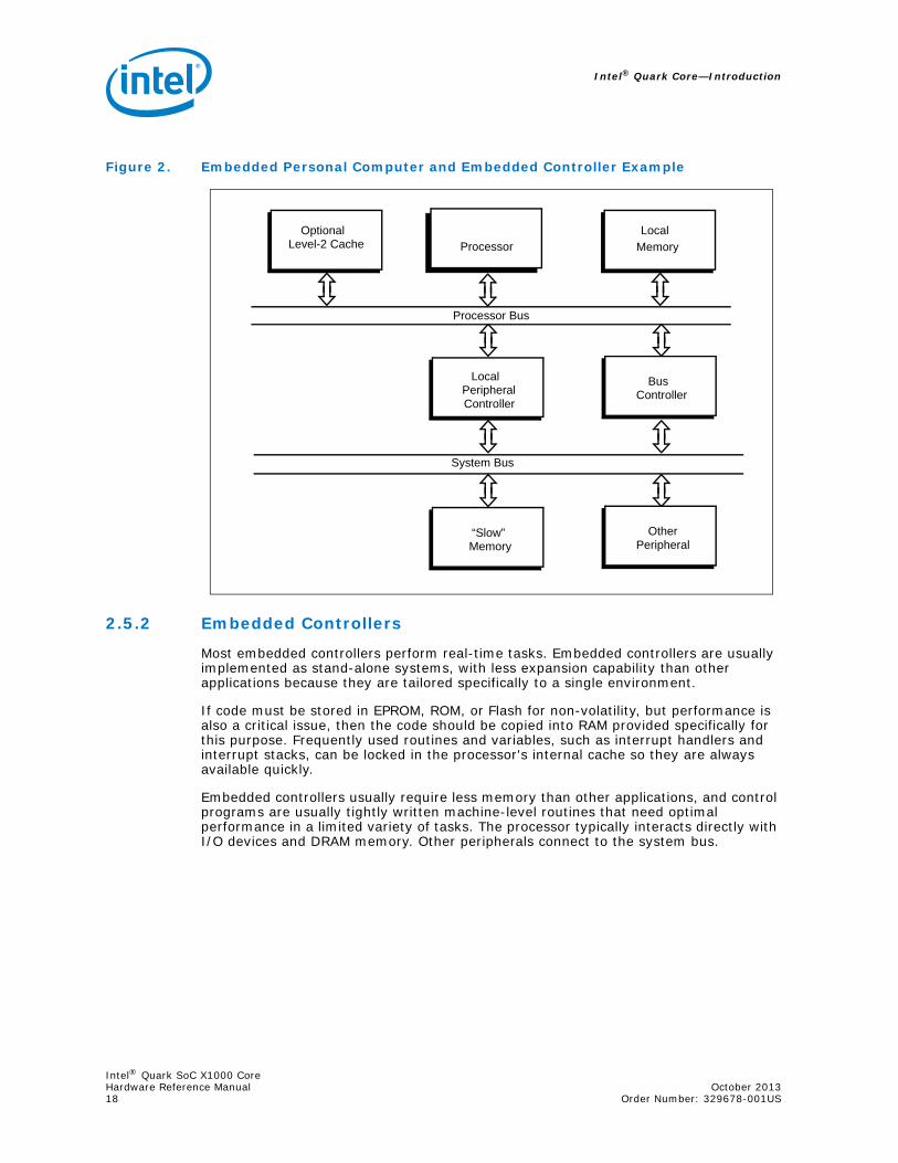
In single-processor embedded systems, the processor interacts with I/O devices and DRAM memory. Conventional personal computer architecture puts most peripherals on separate plug-in boards. Expansion is typically limited to memory boards and I/O boards. A standard I/O architecture such as MCA or EISA is used. System cost and size are very important. Figure 2 shows an example of an embedded personal computer or an embedded controller application.
Figure 1. Intel® Quark SoC X1000 Core used in Intel® Quark SoC X1000
Intel® Quark SoC X1000 CoreOctober 2013 Hardware Reference ManualOrder Number: 329678-001US 17
Intel® Quark Core—Introduction
2.5.2 Embedded Controllers
Most embedded controllers perform real-time tasks. Embedded controllers are usually implemented as stand-alone systems, with less expansion capability than other applications because they are tailored specifically to a single environment.
If code must be stored in EPROM, ROM, or Flash for non-volatility, but performance is also a critical issue, then the code should be copied into RAM provided specifically for this purpose. Frequently used routines and variables, such as interrupt handlers and interrupt stacks, can be locked in the processor's internal cache so they are always available quickly.
Embedded controllers usually require less memory than other applications, and control programs are usually tightly written machine-level routines that need optimal performance in a limited variety of tasks. The processor typically interacts directly with I/O devices and DRAM memory. Other peripherals connect to the system bus.
Figure 2. Embedded Personal Computer and Embedded Controller Example
Processor
Bus
Processor Bus
System Bus
Optional Local
MemoryLevel-2 Cache
LocalPeripheralController
Controller
OtherPeripheral
“Slow”Memory
Intel® Quark SoC X1000 CoreHardware Reference Manual October 201318 Order Number: 329678-001US
Internal Architecture—Intel® Quark Core
3.0 Internal Architecture
The Intel® Quark Core has a 32-bit architecture with on-chip memory management and cache and add clock multiplier and floating-point units. The Intel® Quark Core also supports dynamic bus sizing for the external data bus; that is, the bus size can be specified as 8-, 16-, or 32-bits wide.
Note: The implementation of Intel® Quark Core on Intel® Quark SoC X1000 does not support dynamic bus sizing. Bus width is fixed at 32 bits.
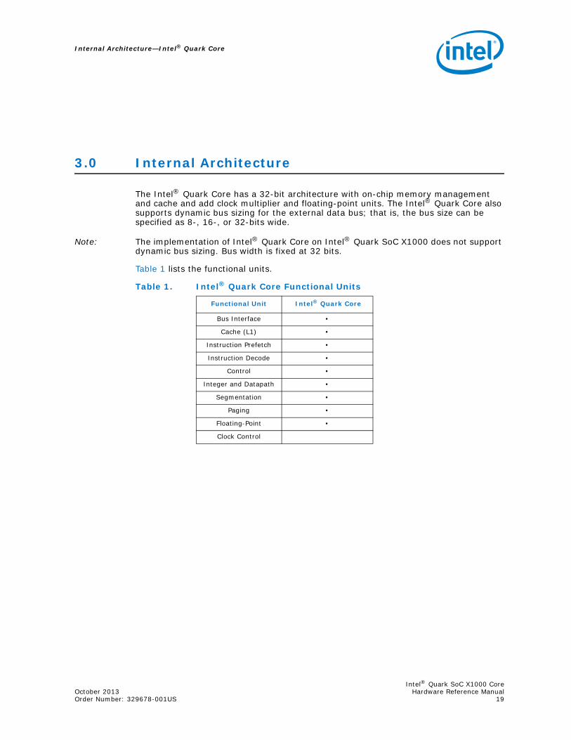
Table 1 lists the functional units.
Table 1. Intel® Quark Core Functional Units
Functional Unit Intel® Quark Core
Bus Interface •
Cache (L1) •
Instruction Prefetch •
Instruction Decode •
Control •
Integer and Datapath •
Segmentation •
Paging •
Floating-Point •
Clock Control
Intel® Quark SoC X1000 CoreOctober 2013 Hardware Reference ManualOrder Number: 329678-001US 19

Intel® Quark Core—Internal Architecture
Figure 3 is a block diagram of the Intel® Quark Core. Note that the cache unit is 16 Kbytes for the Intel® Quark Core.
Signals from the external 32-bit processor bus reach the internal units through the bus interface unit. On the internal side, the bus interface unit and cache unit pass addresses bi-directionally through a 32-bit bus. Data is passed from the cache to the bus interface unit on a 32-bit data bus. The closely coupled cache and instruction prefetch units simultaneously receive instruction prefetches from the bus interface unit over a shared 32-bit data bus, which the cache also uses to receive operands and other types of data. Instructions in the cache are accessible to the instruction prefetch unit, which contains a 32-byte queue of instructions waiting to be executed.
The on-chip cache is 16 Kbytes for the Intel® Quark Core. It is 4-way set associative and follows a write-through policy. The Write-Back Enhanced Intel® Quark Core can be set to use an on-chip write-back cache policy. The on-chip cache includes features to provide flexibility in external memory system design. Individual pages can be designated as cacheable or non-cacheable by software or hardware. The cache can also be enabled and disabled by software or hardware.
Figure 3. Intel® Quark Core Block Diagram
Intel® Quark SoC X1000 CoreHardware Reference Manual October 201320 Order Number: 329678-001US
Internal Architecture—Intel® Quark Core
Internal cache memory allows frequently used data and code to be stored on-chip, reducing accesses to the external bus. A burst bus feature enables fast cache fills.
When internal requests for data or instructions can be satisfied from the cache, time-consuming cycles on the external processor bus are avoided. The bus interface unit is only involved when an operation needs access to the processor bus. Many internal operations are therefore transparent to the external system.
The instruction decode unit translates instructions into low-level control signals and microcode entry points. The control unit executes microcode and controls the integer, floating-point, and segmentation units. Computation results are placed in internal registers within the integer or floating-point units, or in the cache. Internal storage locations (datapaths) are kept in the integer unit.
The cache shares two 32-bit data buses with the segmentation, integer, and floating-point units. These two buses can be used together as a 64-bit inter-unit transfer bus. When 64-bit segment descriptors are passed from the cache to the segmentation unit, 32 bits are passed directly over one data bus and the other 32 bits are passed through the integer unit, so that all 64 bits reach the segmentation unit simultaneously.
The memory management unit (MMU) consists of a segmentation unit and a paging unit which perform address generation. The segmentation unit translates logical addresses and passes them to the paging and cache units on a 32-bit linear address bus. Segmentation allows management of the logical address space by providing easy relocation of data and code and efficient sharing of global resources.
The paging mechanism operates beneath segmentation and is transparent to the segmentation process. The paging unit translates linear addresses into physical addresses, which are passed to the cache on a 20-bit bus. Paging is optional and can be disabled by system software. To implement a virtual memory system, the Intel® Quark Core supports full restartability for all page and segment faults.
Memory is organized into one or more variable length segments, each up to four Gbytes (232 bytes). A segment can have attributes associated with it that include its location, size, type (i.e., stack, code, or data), and protection characteristics. Each task on an Intel® Quark Core can have a maximum of 16,381 segments and each are up to four Gbytes in size. Thus, each task has a maximum of 64 terabytes (trillion bytes) of virtual memory.
The segmentation unit provides four levels of protection for isolating and protecting applications and the operating system from each other. The hardware-enforced protection allows the design of systems with a high degree of software integrity.
The Intel® Quark Core has four modes of operation: Real Address Mode (Real Mode), Protected Mode, Virtual Mode (within Protected Mode), and System Management Mode (SMM). Real Mode is required primarily to set up the Intel® Quark Core for Protected Mode operation.
Protected Mode provides access to the sophisticated memory management paging and privilege capabilities of the processor. Within Protected Mode, software can perform a task switch to enter into tasks designated as Virtual 8086 Mode tasks.
System Management Mode (SMM) provides system designers with a means of adding new software-controlled features to their computer products that always operate transparently to the operating system (OS) and software applications. SMM is intended for use only by system firmware, not by applications software or general purpose systems software.
Intel® Quark SoC X1000 CoreOctober 2013 Hardware Reference ManualOrder Number: 329678-001US 21

Intel® Quark Core—Internal Architecture
3.1 Instruction PipeliningNot every instruction involves all internal units. When an instruction needs the participation of several units, each unit operates in parallel with others on instructions at different stages of execution. Although each instruction is processed sequentially, several instructions are at varying stages of execution in the processor at any given time. This is called instruction pipelining. Instruction prefetch, instruction decode, microcode execution, integer operations, floating-point operations, segmentation, paging, cache management, and bus interface operations are all performed simultaneously. Figure 4 shows some of this parallelism for a single instruction: the instruction fetch, two-stage decode, execution, and register write-back of the execution result. Each stage in this pipeline can occur in one clock cycle.
Figure 4. Internal Pipelining
The internal pipelining on the Intel® Quark Core offers an important performance advantage over many single-clock RISC processors: in the Intel® Quark Core, data can be loaded from the cache with one instruction and used by the next instruction in the next clock. This performance advantage results from the stage-1 decode step, which initiates memory accesses before the execution cycle. Because most compilers and application programs follow load instructions with instructions that operate on the loaded data, this method optimizes the execution of existing binary code.
The method has a performance trade-off: an instruction sequence that changes register contents and then uses that register in the next instruction to access memory takes three clocks rather than two. This trade-off is only a minor disadvantage, however, since most instructions that access memory use the stable contents of the stack pointer or frame pointer, and the additional clock is not used very often. Compilers often place an unrelated instruction between one that changes an addressing register and one that uses the register. Such code is compatible with the Intel® Quark Core provides special stack increment/decrement hardware and an extra register port to execute back-to-back stack push/pop instructions in a single clock.
3.2 Bus Interface Unit The bus interface unit prioritizes and coordinates data transfers, instruction prefetches, and control functions between the processor's internal units and the outside system. Internally, the bus interface unit communicates with the cache and the instruction prefetch units through three 32-bit buses, as shown in Figure 3. Externally, the bus
A5140-01
CLK
InstructionFetch
Stage-1Decode
Stage-2Decode
Execution
RegisterWrite-back
Intel® Quark SoC X1000 CoreHardware Reference Manual October 201322 Order Number: 329678-001US
Internal Architecture—Intel® Quark Core
interface unit provides the processor bus signals, described in Chapter 3. Except for cycle definition signals, all external bus cycles, memory reads, instruction prefetches, cache line fills, etc., look like conventional microprocessor cycles to external hardware, with all cycles having the same bus timing.
The bus interface unit contains the following architectural features:• Address Transceivers and Drivers — The A31–A2 address signals are driven on the
processor bus, together with their corresponding byte-enable signals, BE3#–BE0#. The high-order 28 address signals are bidirectional, allowing external logic to drive cache invalidation addresses into the processor.
• Data Bus Transceivers — The D31–D0 data signals are driven onto and received from the processor bus.
• Bus Size Control — Three sizes of external data bus can be used: 32, 16, and 8 bits wide. Two inputs from external logic specify the width to be used. Bus size can be changed on a cycle-by-cycle basis.
• Write Buffering — Up to four write requests can be buffered, allowing many internal operations to continue without waiting for write cycles to be completed on the processor bus.
• Bus Cycles and Bus Control — A large selection of bus cycles and control functions are supported, including burst transfers, non-burst transfers (single- and multiple-cycle), bus arbitration (bus request, bus hold, bus hold acknowledge, bus locking, bus pseudo-locking, and bus backoff), floating-point error signalling, interrupts, and reset. Two software-controlled outputs enable page caching on a cycle-by-cycle basis. One input and one output are provided for controlling burst read transfers.
• Parity Generation and Control — Even parity is generated on writes to the processor and checked on reads. An error signal indicates a read parity error.
• Cache Control — Cache control and consistency operations are supported. Three inputs allow the external system to control the consistency of data stored in the internal cache unit. Two special bus cycles allow the processor to control the consistency of external cache.Note: The implementation of Intel® Quark Core on Intel® Quark SoC X1000 does
not support external cache.
3.2.1 Data Transfers
To support the cache, the bus interface unit reads 16-byte cacheable transfers of operands, instructions, and other data on the processor bus and passes them to the cache unit. When cache contents are updated from an internal source, such as a register, the bus interface unit writes the updated cache information to the external system. Non-cacheable read transfers are passed through the cache to the integer or floating-point units.
During instruction prefetch, the bus interface unit reads instructions on the processor bus and passes them to both the instruction prefetch unit and the cache. The instruction prefetch unit may then obtain its inputs directly from the cache.
3.2.2 Write Buffers
The bus interface unit has temporary storage for buffering up to four 32-bit write transfers to memory. Addresses, data, or control information can be buffered. Single I/O-mapped writes are not buffered, although multiple I/O writes may be buffered. The buffers can accept memory writes as fast as one per clock. Once a write request is buffered, the internal unit that generated the request is free to continue processing. If no higher-priority request is pending and the bus is free, the transfer is propagated as
Intel® Quark SoC X1000 CoreOctober 2013 Hardware Reference ManualOrder Number: 329678-001US 23

Intel® Quark Core—Internal Architecture
an immediate write cycle to the processor bus. When all four write buffers are full, any subsequent write transfer stalls inside the processor until a write buffer becomes available.
The bus interface unit can re-order pending reads in front of buffered writes. This is done because pending reads can prevent an internal unit from continuing, whereas buffered writes need not have a detrimental effect on processing speed.
Writes are propagated to the processor bus in the first-in-first-out order in which they are received from the internal unit. However, a subsequently generated read request (data or instruction) may be re-ordered in front of buffered writes. As a protection against reading invalid data, this re-ordering of reads in front of buffered writes occurs only if all buffered writes are cache hits. Because an external read is generated only for a cache miss, and is re-ordered in front of buffered writes only if all such buffered writes are cache hits, any read generated on the external bus with this protection never reads a location that is about to be written by a buffered write. This re-ordering can only happen once for a given set of buffered writes, because the data returned by the read cycle could otherwise replace data about to be written from the write buffers.
To ensure that no more than one such re-ordering is done for a given set of buffered writes, all buffered writes are re-flagged as cache misses when a read request is re-ordered ahead of them. Buffered writes thus marked are propagated to the processor bus before the next read request is acted upon. Invalidation of data in the internal cache also causes all pending writes to be flagged as cache misses. Disabling the cache unit disables the write buffers, which eliminates any possibility of re-ordering bus cycles.
3.2.3 Locked Cycles
The processor can generate signals to lock a contiguous series of bus cycles. These cycles can then be performed without interference from other bus masters, if external logic observes these lock signals. One example of a locked operation is a semaphor read-modify-write update, where a resource control register is updated. No other operations should be allowed on the bus until the entire locked semaphor update is completed.
When a locked read cycle is generated, the internal cache is not read. All pending writes in the buffer are completed first. Only then is the read part of the locked operation performed, the data modified, the result placed in a write buffer, and a write cycle performed on the processor bus. This sequence of operations ensures that all writes are performed in the order in which they were generated.
3.2.4 I/O Transfers
Transfers to and from I/O locations have some restrictions to ensure data integrity:• Caching — I/O reads are never cached.• Read Re-ordering — I/O reads are never re-ordered ahead of buffered writes to
memory. This ensures that the processor has completed updating all memory locations before reading status from a device.
• Writes — Single I/O writes are never buffered. When processing an OUT instruction, internal execution stops until all buffered writes and the I/O write are completed on the processor bus. This allows time for external logic to drive a cache invalidate cycle or mask interrupts before the processor executes the next instruction. The processor completes updating all memory locations before writing to the I/O location. Repeated OUT instructions may be buffered.
The Intel® Quark Core does not buffer single I/O writes; a read is not done until the I/O write is completed.
Intel® Quark SoC X1000 CoreHardware Reference Manual October 201324 Order Number: 329678-001US

Internal Architecture—Intel® Quark Core
3.3 Cache UnitThe cache unit stores copies of recently read instructions, operands, and other data. When the processor requests information already in the cache, called a cache hit, no processor-bus cycle is required. When the processor requests information not in the cache, called a cache miss, the information is read into the cache in one or more 16-byte cacheable data transfers, called cache line fills. An internal write request to an area currently in the cache causes two distinct actions if the cache is using a write-through policy: the cache is updated, and the write is also passed through the cache to memory. If the cache is using a write-back policy, then the internal write request only causes the cache to be updated and the write is stored for future main memory updating.
The cache transfers data to other units on two 32-bit buses, as shown in Figure 3. The cache receives linear addresses on a 32-bit bus and the corresponding physical addresses on a 20-bit bus. The cache and instruction prefetch units are closely coupled. 16-Byte blocks of instructions in the cache can be passed quickly to the instruction prefetch unit. Both units read information in 16-byte blocks.
The cache can be accessed as often as once each clock. The cache acts on physical addresses, which minimizes the number of times the cache must be flushed. When both the cache and the cache write-through functions are disabled, the cache may be used as a high-speed RAM.
3.3.1 Cache Structure
The cache has a four-way set associative organization. There are four possible cache locations to store data from a given area of memory. As shown in Figure 5, the 16-Kbyte data block is divided into four data ways, each containing 256 16-byte sets, or cache lines. Each cache line holds data from 16 successive byte addresses in memory, beginning with an address divisible by 16.
Intel® Quark SoC X1000 CoreOctober 2013 Hardware Reference ManualOrder Number: 329678-001US 25

Intel® Quark Core—Internal Architecture
Cache addressing is performed by dividing the high-order 28 bits of the physical address into three parts, as shown in Figure 5. The 8 bits of the index field specify the set number, one of 256, within the cache. The high-order 20 bits on the Intel® Quark Core processor are the tag field; these bits are compared with tags for each cache line in the indexed set, and they indicate whether a 16-byte cache line is stored for that physical address. The low-order 4 bits of the physical address select the byte within the cache line. Finally, a 4-bit valid field, one for each way within a given set, indicates whether the cached data at that physical address is currently valid.
3.3.2 Cache Updating
When a cache miss occurs on a read, the 16-byte block containing the requested information is written into the cache. Data in the neighborhood of the required data is also read into the cache, but the exact position of data within the cache line depends on its location in memory with respect to addresses divisible by 16.
Figure 5. Intel® Quark SoC X1000 Core Cache Organization
Intel® Quark SoC X1000 CoreHardware Reference Manual October 201326 Order Number: 329678-001US

Internal Architecture—Intel® Quark Core
Any area of memory can be cacheable, but any page of memory can be declared not cacheable by setting a bit in its page table entry. The I/O region of memory is non-cacheable. When a read from memory is initiated on the bus, external logic can indicate whether the data may be placed in cache, as discussed in Chapter 4.0, “Bus Operation”. If the read is cacheable, the processor attempts to read an entire 16-byte cache line.
The cache unit follows a write-through cache policy. The unit on the Intel® Quark Core can be configured to be a write-through or write-back cache. Cache line fills are performed only for read misses, never for write misses. When the processor is enabled for normal caching and write- through operation, every internal write to the cache (cache hit) not only updates the cache but is also passed along to the bus interface unit and propagated through the processor bus to memory. The only conditions under which data in the cache differs from the corresponding data in memory occur when a processor write cycle to memory is delayed by buffering in the bus interface unit, or when an external bus master alters the memory area mapped to the internal cache. When the Intel® Quark Core is enabled for normal caching and write-back operation, an internal write only causes the cache to be updated. The modified data is stored for the future update of main memory and is not immediately written to memory.
3.3.3 Cache Replacement
Replacement in the cache is handled by a pseudo-LRU (least recently used) mechanism. This mechanism maintains three bits for each set in the valid/LRU block, as shown in Figure 5. The LRU bits are updated on each cache hit or cache line fill. Each cache line (four per set) also has an associated valid bit that indicates whether the line contains valid data. When the cache is flushed or the processor is reset, all of the valid bits are cleared. When a cache line is to be filled, a location for the fill is selected by simply finding any cache line that is invalid. If no cache line is invalid, the LRU bits select the line to be overwritten. Valid bits are not set for lines that are only partially valid.
Cache lines can be invalidated individually by a cache line invalidation operation on the processor bus. When such an operation is initiated, the cache unit compares the address to be invalidated with tags for the lines currently in cache and clears the valid bit if a match is found. A cache flush operation is also available. This invalidates the entire contents of the internal cache unit.
3.3.4 Cache Configuration
Configuration of the cache unit is controlled by two bits in the processor’s machine status register (CR0). One of these bits enables caching (cache line fills). The other bit enables memory write-through. Table 2 shows the four configuration options. Chapter 4.0, “Bus Operation” gives details.
Table 2. Cache Configuration Options
Cache Enabled Write-through Enabled Operating Mode
no noCache line fills, cache write-throughs, and cache invalidations are disabled. This configuration allows the internal cache to be used as high-speed static RAM.
no yes
Cache line fills are disabled, and cache write-throughs and cache invalidations are enabled. This configuration allows software to disable the cache for a short time, then re-enable it without flushing the original contents.
yes no INVALID
yes yes Cache line fills, cache write-throughs, and cache invalidations are enabled. This is the normal operating configuration.
Intel® Quark SoC X1000 CoreOctober 2013 Hardware Reference ManualOrder Number: 329678-001US 27
Intel® Quark Core—Internal Architecture
When caching is enabled, memory reads and instruction prefetches are cacheable. These transfers are cached if external logic asserts the cache enable input in that bus cycle, and if the current page table entry allows caching. During cycles in which caching is disabled, cache lines are not filled on cache misses. However, the cache remains active even though it is disabled for further filling. Data already in the cache is used if it is still valid. When all data in the cache is flagged invalid, as happens in a cache flush, all internal read requests are propagated as bus cycles to the external system.
When cache write-through is enabled, all writes, including those that are cache hits, are written through to memory. Invalidation operations remove a line from cache if the invalidate address maps to a cache line. When cache write-throughs are disabled, an internal write request that is a cache hit does not cause a write-through to memory, and cache invalidation operations are disabled. With both caching and cache write-through disabled, the cache can be used as a high-speed static RAM. In this configuration, the only write cycles that are propagated to the processor bus are cache misses, and cache invalidation operations are ignored.
The Intel® Quark Core can also be configured to use a write-back cache policy. For detailed information on the Intel® Quark Core cache feature, refer to Chapter 6.0, “Cache Subsystem”.
3.4 Instruction Prefetch UnitWhen the bus interface unit is not performing bus cycles to execute an instruction, the instruction prefetch unit uses the bus interface unit to prefetch instructions. By reading instructions before they are needed, the processor rarely needs to wait for an instruction prefetch cycle on the processor bus.
Instruction prefetch cycles read 16-byte blocks of instructions, starting at addresses numerically greater than the last-fetched instruction. The prefetch unit, which has a direct connection (not shown in Figure 3) to the paging unit, generates the starting address. The 16-byte prefetched blocks are read into both the prefetch and cache units simultaneously. The prefetch queue in the prefetch unit stores 32 bytes of instructions. As each instruction is fetched from the queue, the code part is sent to the instruction decode unit and (depending on the instruction) the displacement part is sent to the segmentation unit, where it is used for address calculation. If loops are encountered in the program being executed, the prefetch unit gets copies of previously executed instructions from the cache.
The prefetch unit has the lowest priority for processor bus access. Assuming zero wait-state memory access, prefetch activity never delays execution. However, if there is no pending data transfer, prefetching may use bus cycles that would otherwise be idle. The prefetch unit is flushed whenever the next instruction needed is not in numerical sequence with the previous instruction; for example, during jumps, task switches, exceptions, and interrupts.
The prefetch unit never accesses beyond the end of a code segment and it never accesses a page that is not present. However, prefetching may cause problems for some hardware mechanisms. For example, prefetching may cause an interrupt when program execution nears the end of memory. To keep prefetching from reading past a given address, instructions should come no closer to that address than one byte plus one aligned 16-byte block.
3.5 Instruction Decode UnitThe instruction decode unit receives instructions from the instruction prefetch unit and translates them in a two-stage process into low-level control signals and microcode entry points, as shown in Figure 3. Most instructions can be decoded at a rate of one per clock. Stage 1 of the decode, shown in Figure 4, initiates a memory access. This
Intel® Quark SoC X1000 CoreHardware Reference Manual October 201328 Order Number: 329678-001US
Internal Architecture—Intel® Quark Core
allows execution of a two-instruction sequence that loads and operates on data in just two clocks, as described in Section 3.2, “Bus Interface Unit” on page 22.
The decode unit simultaneously processes instruction prefix bytes, opcodes, modR/M bytes, and displacements. The outputs include hardwired microinstructions to the segmentation, integer, and floating-point units. The instruction decode unit is flushed whenever the instruction prefetch unit is flushed.
3.6 Control UnitThe control unit interprets the instruction word and microcode entry points received from the instruction decode unit. The control unit has outputs with which it controls the integer and floating-point processing units. It also controls segmentation because segment selection may be specified by instructions.
The control unit contains the processor's microcode. Many instructions have only one line of microcode, so they can execute in an average of one clock cycle. Figure 4 shows how execution fits into the internal pipelining mechanism.
3.7 Integer (Datapath) UnitThe integer and datapath unit identifies where data is stored and performs all of the arithmetic and logical operations available in the processor's instruction set, plus a few new instructions. It has eight 32-bit general-purpose registers, several specialized registers, an ALU, and a barrel shifter. Single load, store, addition, subtraction, logic, and shift instructions execute in one clock.
Two 32-bit bidirectional buses connect the integer and floating-point units. These buses are used together for transferring 64-bit operands. The same buses also connect the processing units with the cache unit. The contents of the general purpose registers are sent to the segmentation unit on a separate 32-bit bus for generation of effective addresses.
3.8 Floating-Point UnitThe floating-point unit executes the same instruction set as the 387 math coprocessor. The unit contains a push-down register stack and dedicated hardware for interpreting the 32-, 64-, and 80-bit formats as specified in IEEE Standard 754. An output signal passed through to the processor bus indicates floating-point errors to the external system, which in turn can assert an input to the processor indicating that the processor should ignore these errors and continue normal operations.
3.8.1 Intel® Quark Core Floating-Point Unit
The Intel® Quark Core incorporates the basic 32-bit architecture, with on-chip memory management and cache memory units. They also have an on-chip floating-point unit (FPU) that operates in parallel with the arithmetic and logic unit. The FPU provides arithmetic instructions for a variety of numeric data types and executes numerous built-in transcendental functions (e.g., tangent, sine, cosine, and log functions). The floating-point unit fully conforms to the ANSI/IEEE standard 754-1985 for floating-point arithmetic.
3.9 Segmentation UnitA segment is a protected, independent address space. Segmentation is used to enforce isolation among application programs, to invoke recovery procedures, and to isolate the effects of programming errors.
Intel® Quark SoC X1000 CoreOctober 2013 Hardware Reference ManualOrder Number: 329678-001US 29

Intel® Quark Core—Internal Architecture
The segmentation unit translates a segmented address issued by a program, called a logical address, into an unsegmented address, called a linear address. The locations of segments in the linear address space are stored in data structures called segment descriptors. The segmentation unit performs its address calculations using segment descriptors and displacements (offsets) extracted from instructions. Linear addresses are sent to the paging and cache units. When a segment is accessed for the first time, its segment descriptor is copied into a processor register. A program can have as many as 16,383 segments. Up to six segment descriptors can be held in processor registers at a time. Figure 6 shows the relationships between logical, linear, and physical addresses.
Figure 6. Segmentation and Paging Address Formats
3.10 Paging UnitThe paging unit allows access to data structures larger than the available memory space by keeping them partly in memory and partly on disk. Paging divides the linear address space into blocks called pages. Paging uses data structures in memory called page tables for mapping a linear address to a physical address. The cache uses physical addresses and puts them on the processor bus. The paging unit also identifies problems, such as accesses to a page that is not resident in memory, and raises exceptions called page faults. When a page fault occurs, the operating system has a chance to bring the required page into memory from disk. If necessary, it can free space in memory by sending another page out to disk. If paging is not enabled, the physical address is identical to the linear address.
Intel® Quark Core supports the following: 4-Kbyte, 2-MB, and 4-MB paging, Supervisor Mode Execution Protection (SMEP), and Execute-Disable Page Protection (PAE.XD).
The paging unit includes a translation lookaside buffer (TLB) that stores the 32 most recently used page table entries. Figure 7 shows the TLB data structures. The paging unit looks up linear addresses in the TLB. If the paging unit does not find a linear address in the TLB, the unit generates requests to fill the TLB with the correct physical address contained in a page table in memory. Only when the correct page table entry is in the TLB does the bus cycle take place. When the paging unit maps a page in the
A5142-01
SegmentSelector
SegmentOffset
047 32 31
Logical Address
Page OffsetPage DirectoryOffset
Page TableOffset
02122
11
111231
Linear Address
Page OffsetPage Base Address
Translated by the segmentation unit
01231
Physical Address
Translated by the paging unit
Intel® Quark SoC X1000 CoreHardware Reference Manual October 201330 Order Number: 329678-001US

Internal Architecture—Intel® Quark Core
linear address space to a page in physical memory, it maps only the upper 20 bits of the linear address. The lowest 12 bits of the physical address come unchanged from the linear address.
Figure 7. Translation Lookaside Buffer
Most programs access only a small number of pages during any short span of time. When this is true, the pages stay in memory and the address translation information stays in the TLB. In typical systems, the TLB satisfies 99% of the requests to access the page tables. The TLB uses a pseudo-LRU algorithm, similar to the cache, as a content-replacement strategy.
The TLB is flushed whenever the page directory base register (CR3) is loaded. Page faults can occur during either a page directory read or a page table read. The cache can be used to supply data for the TLB, although this may not be desirable when external logic monitors TLB updates.
Unlike segmentation, paging is invisible to application programs and does not provide the same kind of protection against programs altering data outside a restricted part of memory. Paging is visible to the operating system, which uses it to satisfy application program memory requirements. For more information on paging and segmentation, see the Intel® Quark SoC X1000 Core Developer’s Manual.
Way 3Way 2Way 1
DataBlock
Way 0Way 3Way 2Way 1
Valid Attributeand Tag Block
A5174-01
LRUBlock
Way 0
Set 7
Set 6
Set 5
Set 4
Set 3
Set 2
Set 1
Set 0
Physical Address
20 Bits
Data
3 Bits
TagAttribute
17 Bits3 Bits1 Bit
Valid
31 1231 121514
Linear Address
Set Select
Intel® Quark SoC X1000 CoreOctober 2013 Hardware Reference ManualOrder Number: 329678-001US 31

Intel® Quark Core—Bus Operation
4.0 Bus Operation
The Intel® Quark Core operates in Standard Bus (write-through) mode. However, when the internal cache is configured in write-back mode, the processor bus operates in Enhanced Bus mode, which is described in Section 4.4.
4.1 Data Transfer MechanismAll data transfers occur as a result of one or more bus cycles. Logical data operands of byte, word and doubleword lengths may be transferred without restrictions on physical address alignment. Data may be accessed at any byte boundary but two or three cycles may be required for unaligned data transfers. (See Section 4.1.2, “Dynamic Data Bus Sizing” on page 34 and Section 4.1.5, “Operand Alignment” on page 40.)
Note: The implementation of Intel® Quark Core on Intel® Quark SoC X1000 does not support dynamic data bus sizing. Bus width is fixed at 32 bits.
The Intel® Quark Core address signals are split into two components. High-order address bits are provided by the address lines, A31–A2. The byte enables, BE3#–BE0#, form the low-order address and provide linear selects for the four bytes of the 32-bit address bus.
The byte enable outputs are asserted when their associated data bus bytes are involved with the present bus cycle, as listed in Table 3. Byte enable patterns that have a deasserted byte enable separating two or three asserted byte enables never occur (see Table 7, “Generating A1, BHE# and BLE# for Addressing 16-Bit Devices” on page 37). All other byte enable patterns are possible.
Address bits A0 and A1 of the physical operand's base address can be created when necessary. Use of the byte enables to create A0 and A1 is shown in Table 4. The byte enables can also be decoded to generate BLE# (byte low enable) and BHE# (byte high enable). These signals are needed to address 16-bit memory systems. (See Section 4.1.3, “Interfacing with 8-, 16-, and 32-Bit Memories” on page 35.)
4.1.1 Memory and I/O Spaces
Bus cycles may access physical memory space or I/O space. Peripheral devices in the system can be either memory-mapped, I/O-mapped, or both. Physical memory addresses range from 00000000H to FFFFFFFFH (4 gigabytes). I/O addresses range from 00000000H to 0000FFFFH (64 Kbytes) for programmed I/O. (See Figure 8.)
Table 3. Byte Enables and Associated Data and Operand Bytes
Byte Enable Signal Associated Data Bus Signals
BE0# D7–D0 (byte 0–least significant)
BE1# D15–D8 (byte 1)
BE2# D23–D16 (byte 2)
BE3# D31–D24 (byte 3–most significant)
Intel® Quark SoC X1000 CoreHardware Reference Manual October 201332 Order Number: 329678-001US
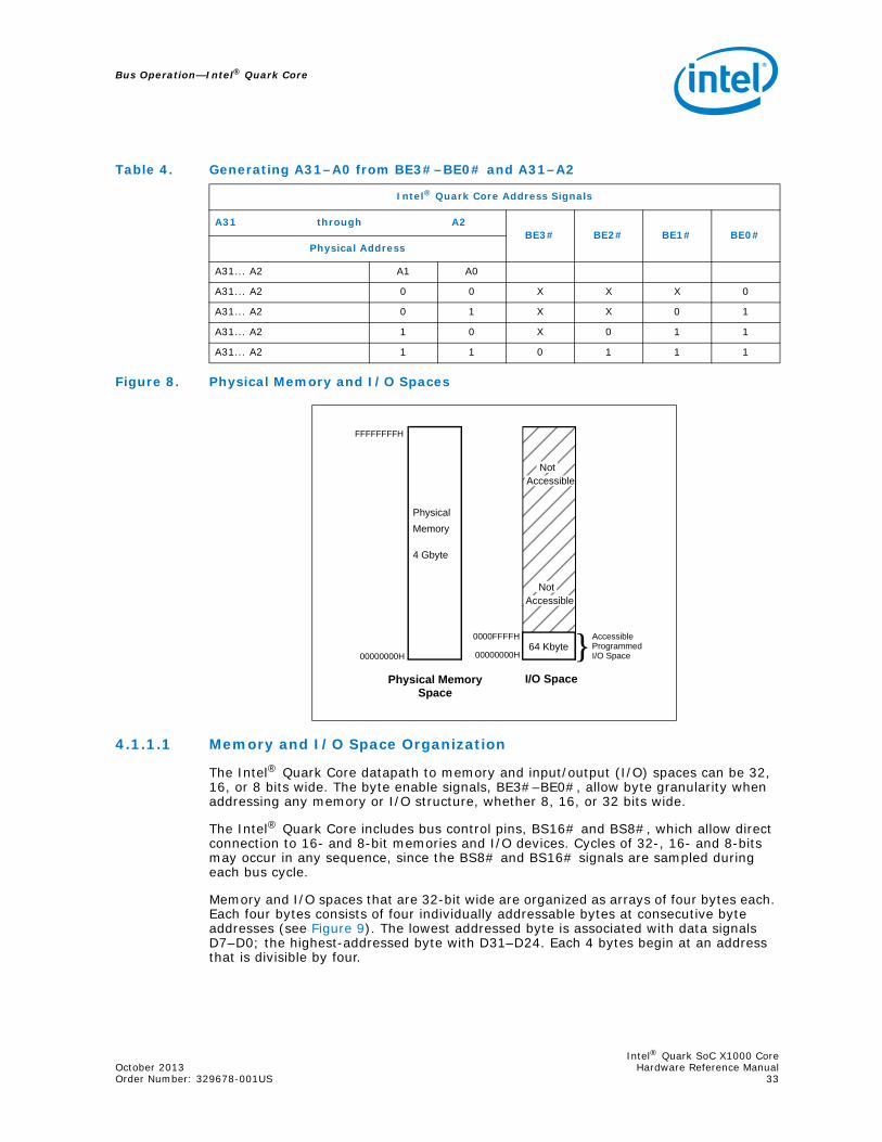
Bus Operation—Intel® Quark Core
Figure 8. Physical Memory and I/O Spaces
4.1.1.1 Memory and I/O Space Organization
The Intel® Quark Core datapath to memory and input/output (I/O) spaces can be 32, 16, or 8 bits wide. The byte enable signals, BE3#–BE0#, allow byte granularity when addressing any memory or I/O structure, whether 8, 16, or 32 bits wide.
The Intel® Quark Core includes bus control pins, BS16# and BS8#, which allow direct connection to 16- and 8-bit memories and I/O devices. Cycles of 32-, 16- and 8-bits may occur in any sequence, since the BS8# and BS16# signals are sampled during each bus cycle.
Memory and I/O spaces that are 32-bit wide are organized as arrays of four bytes each. Each four bytes consists of four individually addressable bytes at consecutive byte addresses (see Figure 9). The lowest addressed byte is associated with data signals D7–D0; the highest-addressed byte with D31–D24. Each 4 bytes begin at an address that is divisible by four.
Table 4. Generating A31–A0 from BE3#–BE0# and A31–A2
Intel® Quark Core Address Signals
A31 through A2BE3# BE2# BE1# BE0#
Physical Address
A31... A2 A1 A0
A31... A2 0 0 X X X 0
A31... A2 0 1 X X 0 1
A31... A2 1 0 X 0 1 1
A31... A2 1 1 0 1 1 1
Physical
Memory
4 Gbyte
NotAccessible
64 Kbyte
{AccessibleProgrammedI/O Space
0000FFFFH
00000000H00000000H
Physical MemorySpace
I/O Space
FFFFFFFFH
NotAccessible
Intel® Quark SoC X1000 CoreOctober 2013 Hardware Reference ManualOrder Number: 329678-001US 33
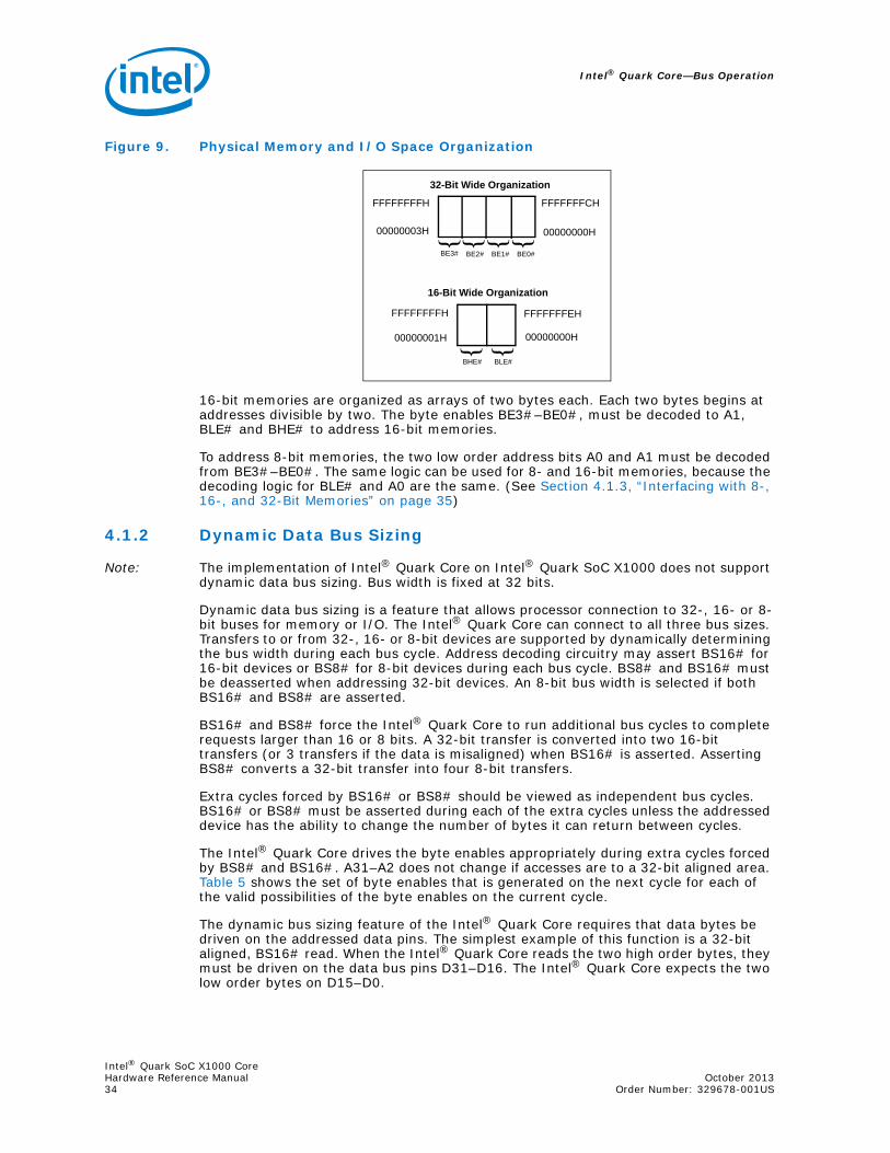
Intel® Quark Core—Bus Operation
Figure 9. Physical Memory and I/O Space Organization
16-bit memories are organized as arrays of two bytes each. Each two bytes begins at addresses divisible by two. The byte enables BE3#–BE0#, must be decoded to A1, BLE# and BHE# to address 16-bit memories.
To address 8-bit memories, the two low order address bits A0 and A1 must be decoded from BE3#–BE0#. The same logic can be used for 8- and 16-bit memories, because the decoding logic for BLE# and A0 are the same. (See Section 4.1.3, “Interfacing with 8-, 16-, and 32-Bit Memories” on page 35)
4.1.2 Dynamic Data Bus Sizing
Note: The implementation of Intel® Quark Core on Intel® Quark SoC X1000 does not support dynamic data bus sizing. Bus width is fixed at 32 bits.
Dynamic data bus sizing is a feature that allows processor connection to 32-, 16- or 8-bit buses for memory or I/O. The Intel® Quark Core can connect to all three bus sizes. Transfers to or from 32-, 16- or 8-bit devices are supported by dynamically determining the bus width during each bus cycle. Address decoding circuitry may assert BS16# for 16-bit devices or BS8# for 8-bit devices during each bus cycle. BS8# and BS16# must be deasserted when addressing 32-bit devices. An 8-bit bus width is selected if both BS16# and BS8# are asserted.
BS16# and BS8# force the Intel® Quark Core to run additional bus cycles to complete requests larger than 16 or 8 bits. A 32-bit transfer is converted into two 16-bit transfers (or 3 transfers if the data is misaligned) when BS16# is asserted. Asserting BS8# converts a 32-bit transfer into four 8-bit transfers.
Extra cycles forced by BS16# or BS8# should be viewed as independent bus cycles. BS16# or BS8# must be asserted during each of the extra cycles unless the addressed device has the ability to change the number of bytes it can return between cycles.
The Intel® Quark Core drives the byte enables appropriately during extra cycles forced by BS8# and BS16#. A31–A2 does not change if accesses are to a 32-bit aligned area. Table 5 shows the set of byte enables that is generated on the next cycle for each of the valid possibilities of the byte enables on the current cycle.
The dynamic bus sizing feature of the Intel® Quark Core requires that data bytes be driven on the addressed data pins. The simplest example of this function is a 32-bit aligned, BS16# read. When the Intel® Quark Core reads the two high order bytes, they must be driven on the data bus pins D31–D16. The Intel® Quark Core expects the two low order bytes on D15–D0.
32-Bit Wide Organization
FFFFFFFFH FFFFFFFCH
16-Bit Wide Organization
FFFFFFFFH FFFFFFFEH
00000001H 00000000H
{ { { {
BE3# BE2# BE1# BE0#
{ {
BHE# BLE#
00000003H 00000000H
Intel® Quark SoC X1000 CoreHardware Reference Manual October 201334 Order Number: 329678-001US

Bus Operation—Intel® Quark Core
The external system must contain buffers to enable the Intel® Quark Core to read and write data on the appropriate data bus pins. Table 6 shows the data bus lines to which the Intel® Quark Core expects data to be returned for each valid combination of byte enables and bus sizing options.
Valid data is only driven onto data bus pins corresponding to asserted byte enables during write cycles. Other pins in the data bus are driven but they contain no valid data. The Intel® Quark Core does not duplicate write data onto parts of the data bus for which the corresponding byte enable is deasserted.
4.1.3 Interfacing with 8-, 16-, and 32-Bit Memories
Note: The implementation of Intel® Quark Core on Intel® Quark SoC X1000 supports 32-bit data mode only.
Table 5. Next Byte Enable Values for BSx# Cycles
Current Next with Next with BS16#
BE3# BE2# BE1# BE0# BE3# BE2# BE1# BE0# BE3# BE2# BE1# BE0#
1 1 1 0 N N N N N N N N
1 1 0 0 1 1 0 1 N N N N
1 0 0 0 1 0 0 1 1 0 1 1
0 0 0 0 0 0 0 1 0 0 1 1
1 1 0 1 N N N N N N N N
1 0 0 1 1 0 1 1 1 0 1 1
0 0 0 1 0 0 1 1 0 0 1 1
1 0 1 1 N N N N N N N N
0 0 1 1 0 1 1 1 N N N N
0 1 1 1 N N N N N N N N
Note: “N” means that another bus cycle is not required to satisfy the request.
Table 6. Data Pins Read with Different Bus Sizes
BE3# BE2# BE1# BE0# w/o BS8#/BS16# w BS8# w BS16#
1 1 1 0 D7–D0 D7–D0 D7–D0
1 1 0 0 D15–D0 D7–D0 D15–D0
1 0 0 0 D23–D0 D7–D0 D15–D0
0 0 0 0 D31–D0 D7–D0 D15–D0
1 1 0 1 D15–D8 D15–D8 D15–D8
1 0 0 1 D23–D8 D15–D8 D15–D8
0 0 0 1 D31–D8 D15–D8 D15–D8
1 0 1 1 D23–D16 D23–D16 D23–D16
0 0 1 1 D31–D16 D23–D16 D31–D16
0 1 1 1 D31–D24 D31–D24 D31–D24
Intel® Quark SoC X1000 CoreOctober 2013 Hardware Reference ManualOrder Number: 329678-001US 35

Intel® Quark Core—Bus Operation
In 32-bit physical memories, such as the one shown in Figure 10, each 4-byte word begins at a byte address that is a multiple of four. A31–A2 are used as a 4-byte word select. BE3#–BE0# select individual bytes within the 4-byte word. BS8# and BS16# are deasserted for all bus cycles involving the 32-bit array.
For 16- and 8-bit memories, byte swapping logic is required for routing data to the appropriate data lines and logic is required for generating BHE#, BLE# and A1. In systems where mixed memory widths are used, extra address decoding logic is necessary to assert BS16# or BS8#.
Figure 10. Intel® Quark Core with 32-Bit Memory
Figure 11 shows the Intel® Quark Core address bus interface to 32-, 16- and 8-bit memories. To address 16-bit memories the byte enables must be decoded to produce A1, BHE# and BLE# (A0). For 8-bit wide memories the byte enables must be decoded to produce A0 and A1. The same byte select logic can be used in 16- and 8-bit systems, because BLE# is exactly the same as A0 (see Table 7).
Figure 11. Addressing 16- and 8-Bit Memories
BE3#–BE0# can be decoded as shown in Table 7. The byte select logic necessary to generate BHE# and BLE# is shown in Figure 12.
Processor32-BitMemory
Data Bus (D31–D0)32
Address Bus(BE3#–BE0#, A31–A2)
BS8# BS16#
“HIGH” “HIGH”
Processor
BS16#BS8#
Address Bus (A31–A2, BE3#–BE0#)
A31–A2
BE3#–BE0#
BHE#, BLE#, A1
A0 (BLE#), A1A31–A2 8-Bit Memory
16-Bit Memory
32-Bit Memory
ByteSelect Logic
AddressDecode
Intel® Quark SoC X1000 CoreHardware Reference Manual October 201336 Order Number: 329678-001US

Bus Operation—Intel® Quark Core
Table 7. Generating A1, BHE# and BLE# for Addressing 16-Bit Devices
Intel® Quark Core 8-, 16-Bit Bus SignalsComments
BE3# BE2# BE1# BE0# A13 BHE#2 BLE# (A0)1
1† 1† 1† 1† x x x x–no asserted bytes
1 1 1 0 0 1 0
1 1 0 1 0 0 1
1 1 0 0 0 0 0
1 0 1 1 1 1 0
1† 0† 1† 0† x x x x–not contiguous bytes
1 0 0 1 0 0 1
1 0 0 0 0 0 0
0 1 1 1 1 0 1
0† 1† 1† 0† x x x x–not contiguous bytes
0† 1† 0† 1† x x x x–not contiguous bytes
0† 1† 0† 0† x x x x–not contiguous bytes
0 1 1 1 0 0
0† 0† 1† 0† x x x x–not contiguous bytes
0 0 0 1 0 0 1
0 0 0 0 0 0 0
Notes:1. BLE# asserted when D7–D0 of 16-bit bus is asserted.2. BHE# asserted when D15–D8 of 16-bit bus is asserted.3. A1 low for all even words; A1 high for all odd words.
KEY:x =don't care† = a non-occurring pattern of byte enables; either none are asserted or the pattern has byte enables asserted for non-contiguous bytes
Intel® Quark SoC X1000 CoreOctober 2013 Hardware Reference ManualOrder Number: 329678-001US 37
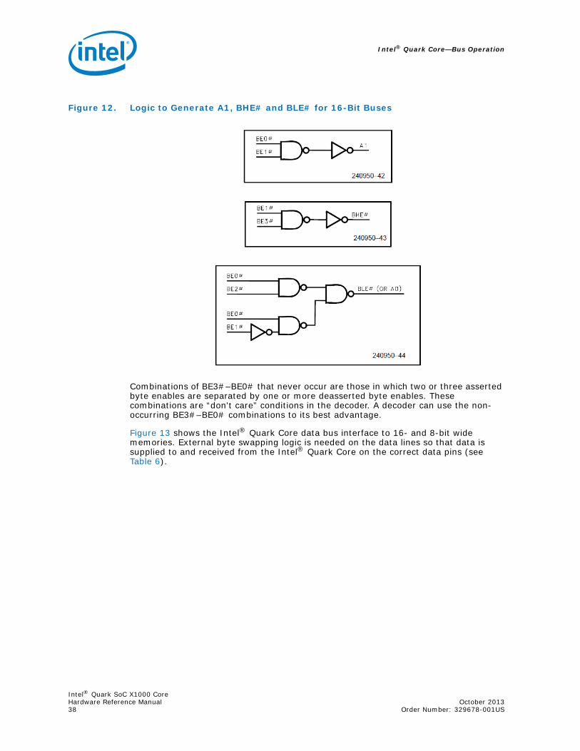
Intel® Quark Core—Bus Operation
Combinations of BE3#–BE0# that never occur are those in which two or three asserted byte enables are separated by one or more deasserted byte enables. These combinations are “don't care” conditions in the decoder. A decoder can use the non-occurring BE3#–BE0# combinations to its best advantage.
Figure 13 shows the Intel® Quark Core data bus interface to 16- and 8-bit wide memories. External byte swapping logic is needed on the data lines so that data is supplied to and received from the Intel® Quark Core on the correct data pins (see Table 6).
Figure 12. Logic to Generate A1, BHE# and BLE# for 16-Bit Buses
Intel® Quark SoC X1000 CoreHardware Reference Manual October 201338 Order Number: 329678-001US

Bus Operation—Intel® Quark Core
Figure 13. Data Bus Interface to 16- and 8-Bit Memories
4.1.4 Dynamic Bus Sizing During Cache Line Fills
Note: The implementation of Intel® Quark Core on Intel® Quark SoC X1000 does not support dynamic data bus sizing. Bus width is fixed at 32 bits.
BS8# and BS16# can be driven during cache line fills. The Intel® Quark Core generates enough 8- or 16-bit cycles to fill the cache line. This can be up to sixteen 8-bit cycles.
The external system should assume that all byte enables are asserted for the first cycle of a cache line fill. The Intel® Quark Core generates proper byte enables for subsequent cycles in the line fill. Table 8 shows the appropriate A0 (BLE#), A1 and BHE# for the various combinations of the Intel® Quark Core byte enables on both the first and subsequent cycles of the cache line fill. The “†” marks all combinations of byte enables that are generated by the Intel® Quark Core during a cache line fill.
Processor
BS16#
BS8#
AddressDecode
32-BitMemory
16-Bit Memory
8-Bit MemoryByte SwapLogic
Byte SwapLogic
16
8
8
8
8
8
D7–D0
D15–D8D23–D16
D31–D24
(A31–A2, BE3#–BE0#)
Table 8. Generating A0, A1 and BHE# from the Intel® Quark Core Byte Enables (Sheet 1 of 2)
BE3# BE2# BE1# BE0#First Cache Fill Cycle Any Other Cycle
A0 A1 BHE# A0 A1 BHE#
1 1 1 0 0 0 0 0 0 1
1 1 0 0 0 0 0 0 0 0
1 0 0 0 0 0 0 0 0 0†0 0 0 0 0 0 0 0 0 0
1 1 0 1 0 0 0 1 0 0
1 0 0 1 0 0 0 1 0 0†0 0 0 1 0 0 0 1 0 0
1 0 1 1 0 0 0 0 1 1
Intel® Quark SoC X1000 CoreOctober 2013 Hardware Reference ManualOrder Number: 329678-001US 39
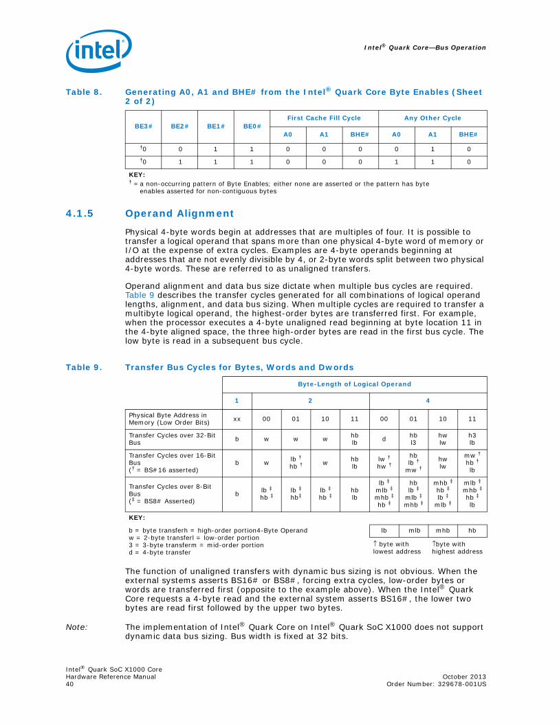
Intel® Quark Core—Bus Operation
4.1.5 Operand Alignment
Physical 4-byte words begin at addresses that are multiples of four. It is possible to transfer a logical operand that spans more than one physical 4-byte word of memory or I/O at the expense of extra cycles. Examples are 4-byte operands beginning at addresses that are not evenly divisible by 4, or 2-byte words split between two physical 4-byte words. These are referred to as unaligned transfers.
Operand alignment and data bus size dictate when multiple bus cycles are required. Table 9 describes the transfer cycles generated for all combinations of logical operand lengths, alignment, and data bus sizing. When multiple cycles are required to transfer a multibyte logical operand, the highest-order bytes are transferred first. For example, when the processor executes a 4-byte unaligned read beginning at byte location 11 in the 4-byte aligned space, the three high-order bytes are read in the first bus cycle. The low byte is read in a subsequent bus cycle.
The function of unaligned transfers with dynamic bus sizing is not obvious. When the external systems asserts BS16# or BS8#, forcing extra cycles, low-order bytes or words are transferred first (opposite to the example above). When the Intel® Quark Core requests a 4-byte read and the external system asserts BS16#, the lower two bytes are read first followed by the upper two bytes.
Note: The implementation of Intel® Quark Core on Intel® Quark SoC X1000 does not support dynamic data bus sizing. Bus width is fixed at 32 bits.
†0 0 1 1 0 0 0 0 1 0†0 1 1 1 0 0 0 1 1 0
KEY:† =a non-occurring pattern of Byte Enables; either none are asserted or the pattern has byte enables asserted for non-contiguous bytes
Table 8. Generating A0, A1 and BHE# from the Intel® Quark Core Byte Enables (Sheet 2 of 2)
BE3# BE2# BE1# BE0#First Cache Fill Cycle Any Other Cycle
A0 A1 BHE# A0 A1 BHE#
Table 9. Transfer Bus Cycles for Bytes, Words and Dwords
Byte-Length of Logical Operand
1 2 4
Physical Byte Address in Memory (Low Order Bits) xx 00 01 10 11 00 01 10 11
Transfer Cycles over 32-Bit Bus b w w w hb
lb d hbl3
hwlw
h3lb
Transfer Cycles over 16-Bit Bus(† = BS#16 asserted)
b w lb †hb † w hb
lblw †hw †
hblb †
mw †hwlw
mw †hb †lb
Transfer Cycles over 8-Bit Bus(‡ = BS8# Asserted)
b lb ‡hb ‡
lb ‡hb‡
lb ‡hb ‡
hblb
lb ‡mlb ‡mhb ‡hb ‡
hblb ‡
mlb ‡mhb ‡
mhb ‡hb ‡lb ‡
mlb ‡
mlb ‡mhb ‡hb ‡lb
KEY:
b = byte transferh = high-order portion4-Byte Operandw = 2-byte transferl = low-order portion3 = 3-byte transferm = mid-order portiond = 4-byte transfer
lb mlb mhb hb
↑ byte with lowest address
↑byte with highest address
Intel® Quark SoC X1000 CoreHardware Reference Manual October 201340 Order Number: 329678-001US

Bus Operation—Intel® Quark Core
In the unaligned transfer described above, the processor requested three bytes on the first cycle. When the external system asserts BS16# during this 3-byte transfer, the lower word is transferred first followed by the upper byte. In the final cycle, the lower byte of the 4-byte operand is transferred, as shown in the 32-bit example above.
4.2 Bus Arbitration Logic Bus arbitration logic is needed with multiple bus masters. Hardware implementations range from single-master designs to those with multiple masters and DMA devices.
Figure 14 shows a simple system in which only one master controls the bus and accesses the memory and I/O devices. Here, no arbitration is required.
Figure 14. Single Master Intel® Quark Core System
Processor
I/O MEM
Control Bus
Data Bus
Address Bus
Intel® Quark SoC X1000 CoreOctober 2013 Hardware Reference ManualOrder Number: 329678-001US 41
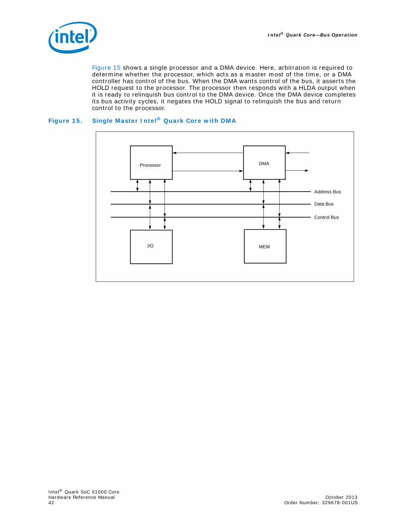
Intel® Quark Core—Bus Operation
Figure 15 shows a single processor and a DMA device. Here, arbitration is required to determine whether the processor, which acts as a master most of the time, or a DMA controller has control of the bus. When the DMA wants control of the bus, it asserts the HOLD request to the processor. The processor then responds with a HLDA output when it is ready to relinquish bus control to the DMA device. Once the DMA device completes its bus activity cycles, it negates the HOLD signal to relinquish the bus and return control to the processor.
Figure 15. Single Master Intel® Quark Core with DMA
Processor DMA
MEMI/O
Address Bus
Data Bus
Control Bus
Intel® Quark SoC X1000 CoreHardware Reference Manual October 201342 Order Number: 329678-001US

Bus Operation—Intel® Quark Core
Figure 16 shows more than one primary bus master and two secondary masters, and the arbitration logic is more complex. The arbitration logic resolves bus contention by ensuring that all device requests are serviced one at a time using either a fixed or a rotating scheme. The arbitration logic then passes information to the Intel® Quark Core, which ultimately releases the bus. The arbitration logic receives bus control status information via the HOLD and HLDA signals and relays it to the requesting devices.
Figure 16. Single Master Intel® Quark Core with Multiple Secondary Masters
As systems become more complex and include multiple bus masters, hardware must be added to arbitrate and assign the management of bus time to each master. The second master may be a DMA controller that requires bus time to perform memory transfers or it may be a second processor that requires the bus to perform memory or I/O cycles. Any of these devices may act as a bus master. The arbitration logic must assign only one bus master at a time so that there is no contention between devices when accessing main memory.
The arbitration logic may be implemented in several different ways. The first technique is to “round-robin” or to “time slice” each master. Each master is given a block of time on the bus to match their priority and need for the bus.
Another method of arbitration is to assign the bus to a master when the bus is needed. Assigning the bus requires the arbitration logic to sample the BREQ or HOLD outputs from the potential masters and to assign the bus to the requestor. A priority scheme must be included to handle cases where more than one device is requesting the bus. The arbitration logic must assert HOLD to the device that must relinquish the bus. Once
Processor DMA
MEMI/O
ArbitrationLogic
ACQ
ACKHLDA 0
HOLD 0
DRQ
DACK
Address Bus
Data Bus
Control Bus
BDCKBREQ
Intel® Quark SoC X1000 CoreOctober 2013 Hardware Reference ManualOrder Number: 329678-001US 43

Intel® Quark Core—Bus Operation
HLDA is asserted by all of these devices, the arbitration logic may assert HLDA or BACK# to the device requesting the bus. The requestor remains the bus master until another device needs the bus.
These two arbitration techniques can be combined to create a more elaborate arbitration scheme that is driven by a device that needs the bus but guarantees that every device gets time on the bus. It is important that an arbitration scheme be selected to best fit the needs of each system's implementation.
The Intel® Quark Core asserts BREQ when it requires control of the bus. BREQ notifies the arbitration logic that the processor has pending bus activity and requests the bus. When its HOLD input is inactive and its HLDA signal is deasserted, the Intel® Quark Core can acquire the bus. Otherwise if HOLD is asserted, then the Intel® Quark Core has to wait for HOLD to be deasserted before acquiring the bus. If the Intel® Quark Core does not have the bus, then its address, data, and status pins are 3-stated. However, the processor can execute instructions out of the internal cache or instruction queue, and does not need control of the bus to remain active.
The address buses shown in Figure 15 and Figure 16 are bidirectional to allow cache invalidations to the processors during memory writes on the bus.
4.3 Bus Functional DescriptionThe Intel® Quark Core supports a wide variety of bus transfers to meet the needs of high performance systems. Bus transfers can be single cycle or multiple cycle, burst or non-burst, cacheable or non-cacheable, 8-, 16- or 32-bit, and pseudo-locked. Cache invalidation cycles and locked cycles provide support for multiprocessor systems.
This section explains basic non-cacheable, non-burst single cycle transfers. It also details multiple cycle transfers and introduces the burst mode. Cacheability is introduced in Section 4.3.3, “Cacheable Cycles” on page 49. The remaining sections describe locked, pseudo-locked, invalidate, bus hold and interrupt cycles.
Bus cycles and data cycles are discussed in this section. A bus cycle is at least two clocks long and begins with ADS# asserted in the first clock and RDY# or BRDY# asserted in the last clock. Data is transferred to or from the Intel® Quark Core during a data cycle. A bus cycle contains one or more data cycles.
Refer to Section 4.3.13, “Bus States” on page 72 for a description of the bus states shown in the timing diagrams.
4.3.1 Non-Cacheable Non-Burst Single Cycle
4.3.1.1 No Wait States
The fastest non-burst bus cycle that the Intel® Quark Core supports is two clocks. These cycles are called 2-2 cycles because reads and writes take two cycles each. The first “2” refers to reads and the second “2” to writes. If a wait state needs to be added to the write, the cycle is called “2-3.”
Basic two-clock read and write cycles are shown in Figure 17. The Intel® Quark Core initiates a cycle by asserting the address status signal (ADS#) at the rising edge of the first clock. The ADS# output indicates that a valid bus cycle definition and address is available on the cycle definition lines and address bus.
Intel® Quark SoC X1000 CoreHardware Reference Manual October 201344 Order Number: 329678-001US
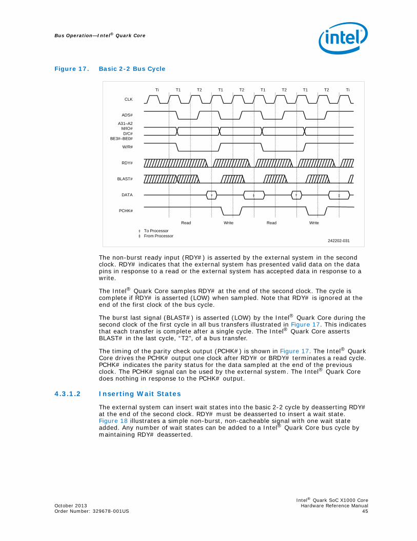
Bus Operation—Intel® Quark Core
Figure 17. Basic 2-2 Bus Cycle
The non-burst ready input (RDY#) is asserted by the external system in the second clock. RDY# indicates that the external system has presented valid data on the data pins in response to a read or the external system has accepted data in response to a write.
The Intel® Quark Core samples RDY# at the end of the second clock. The cycle is complete if RDY# is asserted (LOW) when sampled. Note that RDY# is ignored at the end of the first clock of the bus cycle.
The burst last signal (BLAST#) is asserted (LOW) by the Intel® Quark Core during the second clock of the first cycle in all bus transfers illustrated in Figure 17. This indicates that each transfer is complete after a single cycle. The Intel® Quark Core asserts BLAST# in the last cycle, “T2”, of a bus transfer.
The timing of the parity check output (PCHK#) is shown in Figure 17. The Intel® Quark Core drives the PCHK# output one clock after RDY# or BRDY# terminates a read cycle. PCHK# indicates the parity status for the data sampled at the end of the previous clock. The PCHK# signal can be used by the external system. The Intel® Quark Core does nothing in response to the PCHK# output.
4.3.1.2 Inserting Wait States
The external system can insert wait states into the basic 2-2 cycle by deasserting RDY# at the end of the second clock. RDY# must be deasserted to insert a wait state. Figure 18 illustrates a simple non-burst, non-cacheable signal with one wait state added. Any number of wait states can be added to a Intel® Quark Core bus cycle by maintaining RDY# deasserted.
CLK
ADS#
A31–A2M/IO#D/C#
BE3#–BE0#
W/R#
RDY#
BLAST#
DATA
PCHK#
Ti T1 T2 T1 T2 T1 T2 T1 T2 Ti
Read Write Read Write
To ProcessorFrom Processor‡
†
† † ‡‡
242202-031
Intel® Quark SoC X1000 CoreOctober 2013 Hardware Reference ManualOrder Number: 329678-001US 45

Intel® Quark Core—Bus Operation
Figure 18. Basic 3-3 Bus Cycle
The burst ready input (BRDY#) must be deasserted on all clock edges where RDY# is deasserted for proper operation of these simple non-burst cycles.
4.3.2 Multiple and Burst Cycle Bus Transfers
Multiple cycle bus transfers can be caused by internal requests from the Intel® Quark Core or by the external memory system. An internal request for a 128-bit pre-fetch requires more than one cycle. Internal requests for unaligned data may also require multiple bus cycles. A cache line fill requires multiple cycles to complete.
The external system can cause a multiple cycle transfer when it can only supply 8- or 16-bits per cycle.
Only multiple cycle transfers caused by internal requests are considered in this section. Cacheable cycles and 8- and 16-bit transfers are covered in Section 4.3.3, “Cacheable Cycles” on page 49 and Section 4.3.5, “8- and 16-Bit Cycles” on page 57.
Internal Requests from Intel® Quark Core
An internal request by the Intel® Quark Core for a 64-bit floating-point load must take more than one internal cycle.
4.3.2.1 Burst Cycles
The Intel® Quark Core can accept burst cycles for any bus requests that require more than a single data cycle. During burst cycles, a new data item is strobed into the Intel® Quark Core every clock rather than every other clock as in non-burst cycles. The fastest burst cycle requires two clocks for the first data item, with subsequent data items returned every clock.
CLK
ADS#
A31–A2M/IO#D/C#
BE3#–BE0#
W/R#
RDY#
BLAST#
DATA
Ti T1 T2 Ti
Read Write
To ProcessorFrom Processor
T2 T1 T2 T2
‡†
† ‡
242202-032
Intel® Quark SoC X1000 CoreHardware Reference Manual October 201346 Order Number: 329678-001US
Bus Operation—Intel® Quark Core
The Intel® Quark Core is capable of bursting a maximum of 32 bits during a write. Burst writes can only occur if BS8# or BS16# is asserted. For example, the Intel® Quark Core can burst write four 8-bit operands or two 16-bit operands in a single burst cycle. But the Intel® Quark Core cannot burst multiple 32-bit writes in a single burst cycle.
Burst cycles begin with the Intel® Quark Core driving out an address and asserting ADS# in the same manner as non-burst cycles. The Intel® Quark Core indicates that it is willing to perform a burst cycle by holding the burst last signal (BLAST#) deasserted in the second clock of the cycle. The external system indicates its willingness to do a burst cycle by asserting the burst ready signal (BRDY#).
The addresses of the data items in a burst cycle all fall within the same 16-byte aligned area (corresponding to an internal Intel® Quark Core cache line). A 16-byte aligned area begins at location XXXXXXX0 and ends at location XXXXXXXF. During a burst cycle, only BE3#–BE0#, A2, and A3 may change. A31–A4, M/IO#, D/C#, and W/R# remain stable throughout a burst. Given the first address in a burst, external hardware can easily calculate the address of subsequent transfers in advance. An external memory system can be designed to quickly fill the Intel® Quark Core internal cache lines.
Burst cycles are not limited to cache line fills. Any multiple cycle read request by the Intel® Quark Core can be converted into a burst cycle. The Intel® Quark Core only bursts the number of bytes needed to complete a transfer. For example, the Intel® Quark Core bursts eight bytes for a 64-bit floating-point non-cacheable read.
The external system converts a multiple cycle request into a burst cycle by asserting BRDY# rather than RDY# (non-burst ready) in the first cycle of a transfer. For cycles that cannot be burst, such as interrupt acknowledge and halt, BRDY# has the same effect as RDY#. BRDY# is ignored if both BRDY# and RDY# are asserted in the same clock. Memory areas and peripheral devices that cannot perform bursting must terminate cycles with RDY#.
4.3.2.2 Terminating Multiple and Burst Cycle Transfers
The Intel® Quark Core deasserts BLAST# for all but the last cycle in a multiple cycle transfer. BLAST# is deasserted in the first cycle to inform the external system that the transfer could take additional cycles. BLAST# is asserted in the last cycle of the transfer to indicate that the next time BRDY# or RDY# is asserted the transfer is complete.
BLAST# is not valid in the first clock of a bus cycle. It should be sampled only in the second and subsequent clocks when RDY# or BRDY# is asserted.
The number of cycles in a transfer is a function of several factors including the number of bytes the Intel® Quark Core needs to complete an internal request (1, 2, 4, 8, or 16), the state of the bus size inputs (BS8# and BS16#), the state of the cache enable input (KEN#) and the alignment of the data to be transferred.
When the Intel® Quark Core initiates a request, it knows how many bytes are transferred and if the data is aligned. The external system must indicate whether the data is cacheable (if the transfer is a read) and the width of the bus by returning the state of the KEN#, BS8# and BS16# inputs one clock before RDY# or BRDY# is asserted. The Intel® Quark Core determines how many cycles a transfer will take based on its internal information and inputs from the external system.
BLAST# is not valid in the first clock of a bus cycle because the Intel® Quark Core cannot determine the number of cycles a transfer will take until the external system asserts KEN#, BS8# and BS16#. BLAST# should only be sampled in the second T2 state and subsequent T2 states of a cycle when the external system asserts RDY# or BRDY#.
Intel® Quark SoC X1000 CoreOctober 2013 Hardware Reference ManualOrder Number: 329678-001US 47

Intel® Quark Core—Bus Operation
The system may terminate a burst cycle by asserting RDY# instead of BRDY#. BLAST# remains deasserted until the last transfer. However, any transfers required to complete a cache line fill follow the burst order; for example, if burst order was 4, 0, C, 8 and RDY# was asserted after 0, the next transfers are from C and 8.
4.3.2.3 Non-Cacheable, Non-Burst, Multiple Cycle Transfers
Figure 19 illustrates a two-cycle, non-burst, non-cacheable read. This transfer is simply a sequence of two single cycle transfers. The Intel® Quark Core indicates to the external system that this is a multiple cycle transfer by deasserting BLAST# during the second clock of the first cycle. The external system asserts RDY# to indicate that it will not burst the data. The external system also indicates that the data is not cacheable by deasserting KEN# one clock before it asserts RDY#. When the Intel® Quark Core samples RDY# asserted, it ignores BRDY#.
Figure 19. Non-Cacheable, Non-Burst, Multiple-Cycle Transfers
Each cycle in the transfer begins when ADS# is asserted and the cycle is complete when the external system asserts RDY#.
The Intel® Quark Core indicates the last cycle of the transfer by asserting BLAST#. The next RDY# asserted by the external system terminates the transfer.
4.3.2.4 Non-Cacheable Burst Cycles
The external system converts a multiple cycle request into a burst cycle by asserting BRDY# rather than RDY# in the first cycle of the transfer. This is illustrated in Figure 20.
There are several features to note in the burst read. ADS# is asserted only during the first cycle of the transfer. RDY# must be deasserted when BRDY# is asserted.
CLK
ADS#
A31–A2M/IO#D/C#W/R#
BE3#–BE0#
RDY#
BRDY#
BLAST#
DATA
To Processor†
KEN#
2nd Data
TiT2T1T2T1Ti
1st Data
††
242202-033
Intel® Quark SoC X1000 CoreHardware Reference Manual October 201348 Order Number: 329678-001US

Bus Operation—Intel® Quark Core
BLAST# behaves exactly as it does in the non-burst read. BLAST# is deasserted in the second clock of the first cycle of the transfer, indicating more cycles to follow. In the last cycle, BLAST# is asserted, prompting the external memory system to end the burst after asserting the next BRDY#.
Figure 20. Non-Cacheable Burst Cycle
4.3.3 Cacheable Cycles
Any memory read can become a cache fill operation. The external memory system can allow a read request to fill a cache line by asserting KEN# one clock before RDY# or BRDY# during the first cycle of the transfer on the external bus. Once KEN# is asserted and the remaining three requirements described below are met, the Intel® Quark Core fetches an entire cache line regardless of the state of KEN#. KEN# must be asserted in the last cycle of the transfer for the data to be written into the internal cache. The Intel® Quark Core converts only memory reads or prefetches into a cache fill.
KEN# is ignored during write or I/O cycles. Memory writes are stored only in the on-chip cache if there is a cache hit. I/O space is never cached in the internal cache.
To transform a read or a prefetch into a cache line fill, the following conditions must be met:1. The KEN# pin must be asserted one clock prior to RDY# or BRDY# being asserted
for the first data cycle.2. The cycle must be of a type that can be internally cached. (Locked reads, I/O
reads, and interrupt acknowledge cycles are never cached.)3. The page table entry must have the page cache disable bit (PCD) set to 0. To cache
a page table entry, the page directory must have PCD=0. To cache reads or prefetches when paging is disabled, or to cache the page directory entry, control register 3 (CR3) must have PCD=0.
4. The cache disable (CD) bit in control register 0 (CR0) must be clear.
CLK
ADS#
A31–A2M/IO#D/C#W/R#
BE3#–BE0#
RDY#
BRDY#
BLAST#
DATA
KEN#
TiT2T1T2T1Ti
To Processor†
† †
242202-034
Intel® Quark SoC X1000 CoreOctober 2013 Hardware Reference ManualOrder Number: 329678-001US 49

Intel® Quark Core—Bus Operation
External hardware can determine when the Intel® Quark Core has transformed a read or prefetch into a cache fill by examining the KEN#, M/IO#, D/C#, W/R#, LOCK#, and PCD pins. These pins convey to the system the outcome of conditions 1–3 in the above list. In addition, the Intel® Quark Core drives PCD high whenever the CD bit in CR0 is set, so that external hardware can evaluate condition 4.
Cacheable cycles can be burst or non-burst.
4.3.3.1 Byte Enables during a Cache Line Fill
For the first cycle in the line fill, the state of the byte enables should be ignored. In a non-cacheable memory read, the byte enables indicate the bytes actually required by the memory or code fetch.
The Intel® Quark Core expects to receive valid data on its entire bus (32 bits) in the first cycle of a cache line fill. Data should be returned with the assumption that all the byte enable pins are asserted. However if BS8# is asserted, only one byte should be returned on data lines D7–D0. Similarly if BS16# is asserted, two bytes should be returned on D15–D0.
The Intel® Quark Core generates the addresses and byte enables for all subsequent cycles in the line fill. The order in which data is read during a line fill depends on the address of the first item read. Byte ordering is discussed in Section 4.3.4, “Burst Mode Details” on page 53.
Intel® Quark SoC X1000 CoreHardware Reference Manual October 201350 Order Number: 329678-001US

Bus Operation—Intel® Quark Core
4.3.3.2 Non-Burst Cacheable Cycles
Figure 21 shows a non-burst cacheable cycle. The cycle becomes a cache fill when the Intel® Quark Core samples KEN# asserted at the end of the first clock. The Intel® Quark Core deasserts BLAST# in the second clock in response to KEN#. BLAST# is deasserted because a cache fill requires three additional cycles to complete. BLAST# remains deasserted until the last transfer in the cache line fill. KEN# must be asserted in the last cycle of the transfer for the data to be written into the internal cache.
Note that this cycle would be a single bus cycle if KEN# was not sampled asserted at the end of the first clock. The subsequent three reads would not have happened since a cache fill was not requested.
The BLAST# output is invalid in the first clock of a cycle. BLAST# may be asserted during the first clock due to earlier inputs. Ignore BLAST# until the second clock.
During the first cycle of the cache line fill the external system should treat the byte enables as if they are all asserted. In subsequent cycles in the burst, the Intel® Quark Core drives the address lines and byte enables. (See Section 4.3.4.2, “Burst and Cache Line Fill Order” on page 55.)
Figure 21. Non-Burst, Cacheable Cycles
CLK
ADS#
A31–A2M/IO#D/C#W/R#
BE3#–BE0#
KEN#
RDY#
BLAST#
DATA
Ti T1 T2 T1 T2 T1 T2 T1 T2 Ti
† To Processor
BRDY#
† † ††
242202-035
Intel® Quark SoC X1000 CoreOctober 2013 Hardware Reference ManualOrder Number: 329678-001US 51

Intel® Quark Core—Bus Operation
4.3.3.3 Burst Cacheable Cycles
Figure 22 illustrates a burst mode cache fill. As in Figure 21, the transfer becomes a cache line fill when the external system asserts KEN# at the end of the first clock in the cycle.
The external system informs the Intel® Quark Core that it will burst the line in by asserting BRDY# at the end of the first cycle in the transfer.
Note that during a burst cycle, ADS# is only driven with the first address.
Figure 22. Burst Cacheable Cycle
242202-036
CLK
ADS#
A31–A4M/IO#D/C#W/R#
A3–A2BE3#–BE0#
RDY#
BLAST#
DATA
PCHK#
Ti
To Processor
T1 T2 T2 T2 T2 Ti
KEN#
BRDY#
†
††† †
Intel® Quark SoC X1000 CoreHardware Reference Manual October 201352 Order Number: 329678-001US

Bus Operation—Intel® Quark Core
4.3.3.4 Effect of Changing KEN# during a Cache Line Fill
KEN# can change multiple times as long as it arrives at its final value in the clock before RDY# or BRDY# is asserted. This is illustrated in Figure 23. Note that the timing of BLAST# follows that of KEN# by one clock. The Intel® Quark Core samples KEN# every clock and uses the value returned in the clock before BRDY# or RDY# to determine if a bus cycle would be a cache line fill. Similarly, it uses the value of KEN# in the last cycle before early RDY# to load the line just retrieved from memory into the cache. KEN# is sampled every clock and it must satisfy setup and hold times.
KEN# can also change multiple times before a burst cycle, as long as it arrives at its final value one clock before BRDY# or RDY# is asserted.
Figure 23. Effect of Changing KEN#
4.3.4 Burst Mode Details
4.3.4.1 Adding Wait States to Burst Cycles
Burst cycles need not return data on every clock. The Intel® Quark Core strobes data into the chip only when either RDY# or BRDY# is asserted. Deasserting BRDY# and RDY# adds a wait state to the transfer. A burst cycle where two clocks are required for every burst item is shown in Figure 24.
242202-037
CLK
ADS#
A31–A2M/IO#D/C#W/R#
RDY#
BLAST#
DATA
Ti T1 T2 T2
To Processor
T2 T2 T1 T2
A3–A2BE3#–BE0#
KEN#
†
††
Intel® Quark SoC X1000 CoreOctober 2013 Hardware Reference ManualOrder Number: 329678-001US 53

Intel® Quark Core—Bus Operation
Figure 24. Slow Burst Cycle
242202-038
CLK
ADS#
A31–A2M/IO#D/C#W/R#
KEN#
RDY#
BLAST#
DATA
Ti T1 T2 T2 T2 T2 T2 T2 T2 T2
To Processor
BRDY#
A3–A2BE3#–BE0#
†
† †††
Intel® Quark SoC X1000 CoreHardware Reference Manual October 201354 Order Number: 329678-001US

Bus Operation—Intel® Quark Core
4.3.4.2 Burst and Cache Line Fill Order
The burst order used by the Intel® Quark Core is shown in Table 10. This burst order is followed by any burst cycle (cache or not), cache line fill (burst or not) or code prefetch.
The Intel® Quark Core presents each request for data in an order determined by the first address in the transfer. For example, if the first address was 104 the next three addresses in the burst will be 100, 10C and 108. An example of burst address sequencing is shown in Figure 25.
Figure 25. Burst Cycle Showing Order of Addresses
The sequences shown in Table 10 accommodate systems with 64-bit buses as well as systems with 32-bit data buses. The sequence applies to all bursts, regardless of whether the purpose of the burst is to fill a cache line, perform a 64-bit read, or perform a pre-fetch. If either BS8# or BS16# is asserted, the Intel® Quark Core completes the transfer of the current 32-bit word before progressing to the next 32-bit word. For example, a BS16# burst to address 4 has the following order: 4-6-0-2-C-E-8-A.
Table 10. Burst Order (Both Read and Write Bursts)
First Address Second Address Third Address Fourth Address
0 4 8 C
4 0 C 8
8 C 0 4
C 8 4 0
242202-039
CLK
ADS#
A31–A2
RDY#
BLAST#
DATA
Ti
To Processor
T1 T2 T2 T2 T2 Ti
KEN#
BRDY#
104 100 10C 108
†
† †††
Intel® Quark SoC X1000 CoreOctober 2013 Hardware Reference ManualOrder Number: 329678-001US 55

Intel® Quark Core—Bus Operation
4.3.4.3 Interrupted Burst Cycles
Some memory systems may not be able to respond with burst cycles in the order defined in Table 10. To support these systems, the Intel® Quark Core allows a burst cycle to be interrupted at any time. The Intel® Quark Core automatically generates another normal bus cycle after being interrupted to complete the data transfer. This is called an interrupted burst cycle. The external system can respond to an interrupted burst cycle with another burst cycle.
The external system can interrupt a burst cycle by asserting RDY# instead of BRDY#. RDY# can be asserted after any number of data cycles terminated with BRDY#.
An example of an interrupted burst cycle is shown in Figure 26. The Intel® Quark Core immediately asserts ADS# to initiate a new bus cycle after RDY# is asserted. BLAST# is deasserted one clock after ADS# begins the second bus cycle, indicating that the transfer is not complete.
Figure 26. Interrupted Burst Cycle
KEN# need not be asserted in the first data cycle of the second part of the transfer shown in Figure 27. The cycle had been converted to a cache fill in the first part of the transfer and the Intel® Quark Core expects the cache fill to be completed. Note that the first half and second half of the transfer in Figure 26 are both two-cycle burst transfers.
The order in which the Intel® Quark Core requests operands during an interrupted burst transfer is shown by Table 9, “Transfer Bus Cycles for Bytes, Words and Dwords” on page 40. Mixing RDY# and BRDY# does not change the order in which operand addresses are requested by the Intel® Quark Core.
An example of the order in which the Intel® Quark Core requests operands during a cycle in which the external system mixes RDY# and BRDY# is shown in Figure 27. The Intel® Quark Core initially requests a transfer beginning at location 104. The transfer becomes a cache line fill when the external system asserts KEN#. The first cycle of the cache fill transfers the contents of location 104 and is terminated with RDY#. The
242202-067
CLK
ADS#
A31–A2
BRDY#
BLAST#
DATA
Ti T1 T2 Ti
To Processor
T2 T1 T2 T2
KEN#
RDY#
104 100 10C 108
†
† † ††
Intel® Quark SoC X1000 CoreHardware Reference Manual October 201356 Order Number: 329678-001US

Bus Operation—Intel® Quark Core
Intel® Quark Core drives out a new request (by asserting ADS#) to address 100. If the external system terminates the second cycle with BRDY#, the Intel® Quark Core next requests/expects address 10C. The correct order is determined by the first cycle in the transfer, which may not be the first cycle in the burst if the system mixes RDY# with BRDY#.
Figure 27. Interrupted Burst Cycle with Non-Obvious Order of Addresses
4.3.5 8- and 16-Bit Cycles
The Intel® Quark Core supports both 16- and 8-bit external buses through the BS16# and BS8# inputs. BS16# and BS8# allow the external system to specify, on a cycle-by-cycle basis, whether the addressed component can supply 8, 16 or 32 bits. BS16# and BS8# can be used in burst cycles as well as non-burst cycles. If both BS16# and BS8# are asserted for any bus cycle, the Intel® Quark Core responds as if only BS8# is asserted.
The timing of BS16# and BS8# is the same as that of KEN#. BS16# and BS8# must be asserted before the first RDY# or BRDY# is asserted. Asserting BS16# and BS8# can force the Intel® Quark Core to run additional cycles to complete what would have been only a single 32-bit cycle. BS8# and BS16# may change the state of BLAST# when they force subsequent cycles from the transfer.
Figure 28 shows an example in which BS8# forces the Intel® Quark Core to run two extra cycles to complete a transfer. The Intel® Quark Core issues a request for 24 bits of information. The external system asserts BS8#, indicating that only eight bits of data can be supplied per cycle. The Intel® Quark Core issues two extra cycles to complete the transfer.
242202-068
CLK
ADS#
A31–A2
BRDY#
BLAST#
DATA
Ti T1 T2 Ti
To Processor
T1 T2 T2 T2
KEN#
RDY#
104 100 10C 108
†
† † † †
Intel® Quark SoC X1000 CoreOctober 2013 Hardware Reference ManualOrder Number: 329678-001US 57

Intel® Quark Core—Bus Operation
Figure 28. 8-Bit Bus Size Cycle
Extra cycles forced by BS16# and BS8# signals should be viewed as independent bus cycles. BS16# and BS8# should be asserted for each additional cycle unless the addressed device can change the number of bytes it can return between cycles. The Intel® Quark Core deasserts BLAST# until the last cycle before the transfer is complete.
Refer to Section 4.1.2, “Dynamic Data Bus Sizing” on page 34 for the sequencing of addresses when BS8# or BS16# are asserted.
During burst cycles, BS8# and BS16# operate in the same manner as during non-burst cycles. For example, a single non-cacheable read could be transferred by the Intel® Quark Core as four 8-bit burst data cycles. Similarly, a single 32-bit write could be written as four 8-bit burst data cycles. An example of a burst write is shown in Figure 29. Burst writes can only occur if BS8# or BS16# is asserted.
242202-069
CLK
ADS#
A31–A2M/IO#D/C#W/R#
RDY#
BLAST#
DATA
Ti T1 T2 Ti
To Processor
T1 T2 T1 T2
BS8#
BE3#–BE0#
†
† † †
Intel® Quark SoC X1000 CoreHardware Reference Manual October 201358 Order Number: 329678-001US

Bus Operation—Intel® Quark Core
Figure 29. Burst Write as a Result of BS8# or BS16#
4.3.6 Locked Cycles
Locked cycles are generated in software for any instruction that performs a read-modify-write operation. During a read-modify-write operation, the Intel® Quark Core can read and modify a variable in external memory and ensure that the variable is not accessed between the read and write.
Locked cycles are automatically generated during certain bus transfers. The XCHG (exchange) instruction generates a locked cycle when one of its operands is memory-based. Locked cycles are generated when a segment or page table entry is updated and during interrupt acknowledge cycles. Locked cycles are also generated when the LOCK instruction prefix is used with selected instructions.
Locked cycles are implemented in hardware with the LOCK# pin. When LOCK# is asserted, the Intel® Quark Core is performing a read-modify-write operation and the external bus should not be relinquished until the cycle is complete. Multiple reads or writes can be locked. A locked cycle is shown in Figure 30. LOCK# is asserted with the address and bus definition pins at the beginning of the first read cycle and remains asserted until RDY# is asserted for the last write cycle. For unaligned 32-bit read-modify-write operations, the LOCK# remains asserted for the entire duration of the multiple cycle. It deasserts when RDY# is asserted for the last write cycle.
When LOCK# is asserted, the Intel® Quark Core recognizes address hold and backoff but does not recognize bus hold. It is left to the external system to properly arbitrate a central bus when the Intel® Quark Core generates LOCK#.
242202–143
CLK
ADS#
BE3#–BE0#
RDY#
BLAST#
DATA
Ti
From Processor
T1 T2 T2 T2 T2 Ti
BS8#
BRDY#
ADDRSPEC
‡
‡
Intel® Quark SoC X1000 CoreOctober 2013 Hardware Reference ManualOrder Number: 329678-001US 59
Intel® Quark Core—Bus Operation
Figure 30. Locked Bus Cycle
4.3.7 Pseudo-Locked Cycles
Pseudo-locked cycles assure that no other master is given control of the bus during operand transfers that take more than one bus cycle.
For the Intel® Quark Core, examples include 64-bit description loads and cache line fills.
Pseudo-locked transfers are indicated by the PLOCK# pin. The memory operands must be aligned for correct operation of a pseudo-locked cycle.
PLOCK# need not be examined during burst reads. A 64-bit aligned operand can be retrieved in one burst (note that this is only valid in systems that do not interrupt bursts).
The system must examine PLOCK# during 64-bit writes since the Intel® Quark Core cannot burst write more than 32 bits. However, burst can be used within each 32-bit write cycle if BS8# or BS16# is asserted. BLAST is de-asserted in response to BS8# or BS16#. A 64-bit write is driven out as two non-burst bus cycles. BLAST# is asserted during both 32-bit writes, because a burst is not possible. PLOCK# is asserted during the first write to indicate that another write follows. This behavior is shown in Figure 31.
The first cycle of a 64-bit floating-point write is the only case in which both PLOCK# and BLAST# are asserted. Normally PLOCK# and BLAST# are the inverse of each other.
During all of the cycles in which PLOCK# is asserted, HOLD is not acknowledged until the cycle completes. This results in a large HOLD latency, especially when BS8# or BS16# is asserted. To reduce the HOLD latency during these cycles, windows are available between transfers to allow HOLD to be acknowledged during non-cacheable code prefetches. PLOCK# is asserted because BLAST# is deasserted, but PLOCK# is ignored and HOLD is recognized during the prefetch.
242202-080
TiT2T1T2T1Ti
CLK
ADS#
A31–A2M/IO#D/C#
BE3#–BE0#
W/R#
RDY#
DATA
LOCK#
To ProcessorFrom Processor
Read Write
‡†
† ‡
Intel® Quark SoC X1000 CoreHardware Reference Manual October 201360 Order Number: 329678-001US

Bus Operation—Intel® Quark Core
PLOCK# can change several times during a cycle, settling to its final value in the clock in which RDY# is asserted.
4.3.7.1 Floating-Point Read and Write Cycles
For the Intel® Quark Core, 64-bit floating-point read and write cycles are also examples of operand transfers that take more than one bus cycle.
Figure 31. Pseudo Lock Timing
4.3.8 Invalidate Cycles
Invalidate cycles keep the Intel® Quark Core internal cache contents consistent with external memory. The Intel® Quark Core contains a mechanism for monitoring writes by other devices to external memory. When the Intel® Quark Core finds a write to a section of external memory contained in its internal cache, the Intel® Quark Core's internal copy is invalidated.
Invalidations use two pins, address hold request (AHOLD) and valid external address (EADS#). There are two steps in an invalidation cycle. First, the external system asserts the AHOLD input forcing the Intel® Quark Core to immediately relinquish its address bus. Next, the external system asserts EADS#, indicating that a valid address is on the Intel® Quark Core address bus. Figure 32 shows the fastest possible invalidation cycle. The Intel® Quark Core recognizes AHOLD on one CLK edge and floats the address bus in response. To allow the address bus to float and avoid contention, EADS# and the invalidation address should not be driven until the following CLK edge. The Intel® Quark Core reads the address over its address lines. If the Intel® Quark Core finds this address in its internal cache, the cache entry is invalidated. Note that the Intel® Quark Core address bus is input/output.
TiT2T1T2T1Ti
CLK
ADS#
A31–A2M/IO#D/C#
BE3#–BE0#
W/R#
RDY#
BLAST#
From Processor
DATA
PLOCK#
Write Write
‡
‡ ‡
242202-144
Intel® Quark SoC X1000 CoreOctober 2013 Hardware Reference ManualOrder Number: 329678-001US 61

Intel® Quark Core—Bus Operation
Figure 32. Fast Internal Cache Invalidation Cycle
Figure 33. Typical Internal Cache Invalidation Cycle
242202-091
CLK
ADS#
ADDR
BREQ
DATA
Ti T1 T2 Ti
To Processor†
Ti Ti T1 T2
EADS#
AHOLD
RDY#
† †
†
242202-092
CLK
ADS#
ADDR
RDY#
BREQ
DATA
Ti T1 T2 T2
To Processor
Ti Ti T1 T1
EADS#
AHOLD
†
†
†
Intel® Quark SoC X1000 CoreHardware Reference Manual October 201362 Order Number: 329678-001US
Bus Operation—Intel® Quark Core
4.3.8.1 Rate of Invalidate Cycles
The Intel® Quark Core can accept one invalidate per clock except in the last clock of a line fill. One invalidate per clock is possible as long as EADS# is deasserted in ONE or BOTH of the following cases:1. In the clock in which RDY# or BRDY# is asserted for the last time.2. In the clock following the clock in which RDY# or BRDY# is asserted for the last
time.
This definition allows two system designs. Simple designs can restrict invalidates to one every other clock. The simple design need not track bus activity. Alternatively, systems can request one invalidate per clock provided that the bus is monitored.
4.3.8.2 Running Invalidate Cycles Concurrently with Line Fills
Precautions are necessary to avoid caching stale data in the Intel® Quark Core cache in a system with a second-level cache. An example of a system with a second-level cache is shown in Figure 34.
Note: The implementation of Intel® Quark Core on Intel® Quark SoC X1000 does not support second-level cache.
An external device can write to main memory over the system bus while the Intel® Quark Core is retrieving data from the second-level cache. The Intel® Quark Core must invalidate a line in its internal cache if the external device is writing to a main memory address that is also contained in the Intel® Quark Core cache.
A potential problem exists if the external device is writing to an address in external memory, and at the same time the Intel® Quark Core is reading data from the same address in the second-level cache. The system must force an invalidation cycle to invalidate the data that the Intel® Quark Core has requested during the line fill.
Intel® Quark SoC X1000 CoreOctober 2013 Hardware Reference ManualOrder Number: 329678-001US 63
Intel® Quark Core—Bus Operation
Figure 34. System with Second-Level Cache
Processor
Second-LevelCache
System Bus
ExternalMemory
External BusMaster
Address, Data andControl Bus
Address, Data andControl Bus
Intel® Quark SoC X1000 CoreHardware Reference Manual October 201364 Order Number: 329678-001US

Bus Operation—Intel® Quark Core
If the system asserts EADS# before the first data in the line fill is returned to the Intel® Quark Core, the system must return data consistent with the new data in the external memory upon resumption of the line fill after the invalidation cycle. This is illustrated by the asserted EADS# signal labeled “1” in Figure 35.
If the system asserts EADS# at the same time or after the first data in the line fill is returned (in the same clock that the first RDY# or BRDY# is asserted or any subsequent clock in the line fill) the data is read into the Intel® Quark Core input buffers but it is not stored in the on-chip cache. This is illustrated by asserted EADS# signal labeled “2” in Figure 35. The stale data is used to satisfy the request that initiated the cache fill cycle.
Figure 35. Cache Invalidation Cycle Concurrent with Line Fill
242202-093
NOTES:1. Data returned must be consistent if its address equals the invalidation address in this clock.2. Data returned is not cached if its address equals the invalidation address in this clock.
CLK
ADS#
ADDR
AHOLD
RDY#
DATA
Ti T1 T2 T2 T2 T2 T2 T2 Ti
To Processor
EADS#
1 2
BRDY#
KEN#
†
† †††
††
Intel® Quark SoC X1000 CoreOctober 2013 Hardware Reference ManualOrder Number: 329678-001US 65
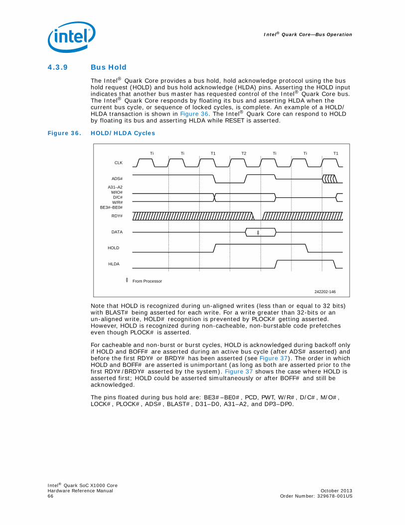
Intel® Quark Core—Bus Operation
4.3.9 Bus Hold
The Intel® Quark Core provides a bus hold, hold acknowledge protocol using the bus hold request (HOLD) and bus hold acknowledge (HLDA) pins. Asserting the HOLD input indicates that another bus master has requested control of the Intel® Quark Core bus. The Intel® Quark Core responds by floating its bus and asserting HLDA when the current bus cycle, or sequence of locked cycles, is complete. An example of a HOLD/HLDA transaction is shown in Figure 36. The Intel® Quark Core can respond to HOLD by floating its bus and asserting HLDA while RESET is asserted.
Figure 36. HOLD/HLDA Cycles
Note that HOLD is recognized during un-aligned writes (less than or equal to 32 bits) with BLAST# being asserted for each write. For a write greater than 32-bits or an un-aligned write, HOLD# recognition is prevented by PLOCK# getting asserted. However, HOLD is recognized during non-cacheable, non-burstable code prefetches even though PLOCK# is asserted.
For cacheable and non-burst or burst cycles, HOLD is acknowledged during backoff only if HOLD and BOFF# are asserted during an active bus cycle (after ADS# asserted) and before the first RDY# or BRDY# has been asserted (see Figure 37). The order in which HOLD and BOFF# are asserted is unimportant (as long as both are asserted prior to the first RDY#/BRDY# asserted by the system). Figure 37 shows the case where HOLD is asserted first; HOLD could be asserted simultaneously or after BOFF# and still be acknowledged.
The pins floated during bus hold are: BE3#–BE0#, PCD, PWT, W/R#, D/C#, M/O#, LOCK#, PLOCK#, ADS#, BLAST#, D31–D0, A31–A2, and DP3–DP0.
242202-146
CLK
ADS#
A31–A2M/IO#D/C#W/R#
BE3#–BE0#
RDY#
DATA
HLDA
Ti
From Processor
Ti T1 T2 Ti Ti T1
‡
HOLD
‡
Intel® Quark SoC X1000 CoreHardware Reference Manual October 201366 Order Number: 329678-001US

Bus Operation—Intel® Quark Core
Figure 37. HOLD Request Acknowledged during BOFF#
4.3.10 Interrupt Acknowledge
The Intel® Quark Core generates interrupt acknowledge cycles in response to maskable interrupt requests that are generated on the interrupt request input (INTR) pin. Interrupt acknowledge cycles have a unique cycle type generated on the cycle type pins.
An example of an interrupt acknowledge transaction is shown in Figure 38. Interrupt acknowledge cycles are generated in locked pairs. Data returned during the first cycle is ignored. The interrupt vector is returned during the second cycle on the lower 8 bits of the data bus. The Intel® Quark Core has 256 possible interrupt vectors.
The state of A2 distinguishes the first and second interrupt acknowledge cycles. The byte address driven during the first interrupt acknowledge cycle is 4 (A31–A3 low, A2 high, BE3#–BE1# high, and BE0# low). The address driven during the second interrupt acknowledge cycle is 0 (A31–A2 low, BE3#–BE1# high, BE0# low).
Each of the interrupt acknowledge cycles is terminated when the external system asserts RDY# or BRDY#. Wait states can be added by holding RDY# or BRDY# deasserted. The Intel® Quark Core automatically generates four idle clocks between the first and second cycles to allow for 8259A recovery time.
242202-095
CLK
ADS#
M/IO#
D/C#
KEN#
BRDY#
RDY#
W/R#
HOLD
HLDA
BOFF#
Ti Ti Ti Ti Ti T1 T2 Ti Ti Ti Ti
Intel® Quark SoC X1000 CoreOctober 2013 Hardware Reference ManualOrder Number: 329678-001US 67

Intel® Quark Core—Bus Operation
Figure 38. Interrupt Acknowledge Cycles
4.3.11 Special Bus Cycles
The Intel® Quark Core provides special bus cycles to indicate that certain instructions have been executed, or certain conditions have occurred internally. The special bus cycles are identified by the status of the pins shown in Table 11.
During these cycles the address bus is driven low while the data bus is undefined.
Two of the special cycles indicate halt or shutdown. Another special cycle is generated when the Intel® Quark Core executes an INVD (invalidate data cache) instruction and could be used to flush an external cache. The Write Back cycle is generated when the Intel® Quark Core executes the WBINVD (write-back invalidate data cache) instruction and could be used to synchronize an external write-back cache.
Note: The implementation of Intel® Quark Core on Intel® Quark SoC X1000 does not support external cache.
The external hardware must acknowledge these special bus cycles by asserting RDY# or BRDY#.
4.3.11.1 HALT Indication Cycle
The Intel® Quark Core halts as a result of executing a HALT instruction. A HALT indication cycle is performed to signal that the processor has entered into the HALT state. The HALT indication cycle is identified by the bus definition signals in special bus cycle state and by a byte address of 2. BE0# and BE2# are the only signals that distinguish HALT indication from shutdown indication, which drives an address of 0. During the HALT cycle, undefined data is driven on D31–D0. The HALT indication cycle must be acknowledged by RDY# asserted.
A halted Intel® Quark Core resumes execution when INTR (if interrupts are enabled), NMI, or RESET is asserted.
CLK
ADS#
ADDR
RDY#
DATA
Ti T1 T2 Ti Ti T1 T2 Ti
To Processor†
LOCK#
4 Clocks
†
04 00
242202-096
Intel® Quark SoC X1000 CoreHardware Reference Manual October 201368 Order Number: 329678-001US
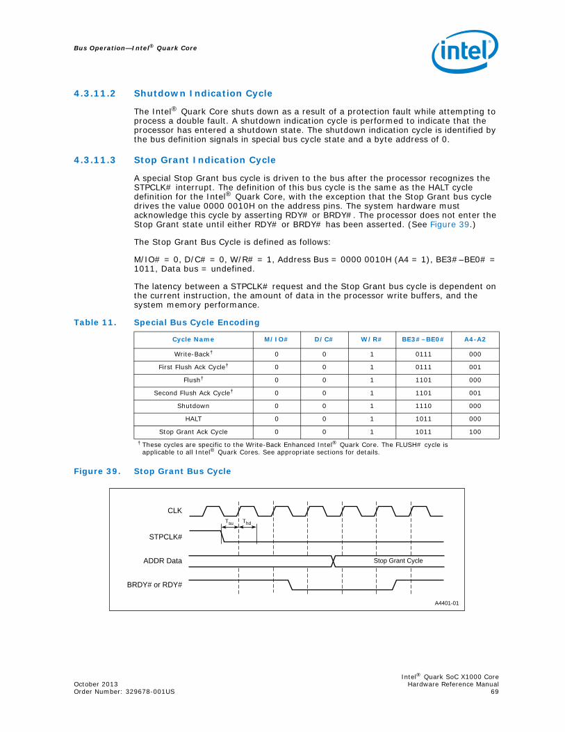
Bus Operation—Intel® Quark Core
4.3.11.2 Shutdown Indication Cycle
The Intel® Quark Core shuts down as a result of a protection fault while attempting to process a double fault. A shutdown indication cycle is performed to indicate that the processor has entered a shutdown state. The shutdown indication cycle is identified by the bus definition signals in special bus cycle state and a byte address of 0.
4.3.11.3 Stop Grant Indication Cycle
A special Stop Grant bus cycle is driven to the bus after the processor recognizes the STPCLK# interrupt. The definition of this bus cycle is the same as the HALT cycle definition for the Intel® Quark Core, with the exception that the Stop Grant bus cycle drives the value 0000 0010H on the address pins. The system hardware must acknowledge this cycle by asserting RDY# or BRDY#. The processor does not enter the Stop Grant state until either RDY# or BRDY# has been asserted. (See Figure 39.)
The Stop Grant Bus Cycle is defined as follows:
M/IO# = 0, D/C# = 0, W/R# = 1, Address Bus = 0000 0010H (A4 = 1), BE3#–BE0# = 1011, Data bus = undefined.
The latency between a STPCLK# request and the Stop Grant bus cycle is dependent on the current instruction, the amount of data in the processor write buffers, and the system memory performance.
Figure 39. Stop Grant Bus Cycle
Table 11. Special Bus Cycle Encoding
Cycle Name M/IO# D/C# W/R# BE3#–BE0# A4-A2
Write-Back† 0 0 1 0111 000
First Flush Ack Cycle† 0 0 1 0111 001
Flush† 0 0 1 1101 000
Second Flush Ack Cycle† 0 0 1 1101 001
Shutdown 0 0 1 1110 000
HALT 0 0 1 1011 000
Stop Grant Ack Cycle 0 0 1 1011 100† These cycles are specific to the Write-Back Enhanced Intel® Quark Core. The FLUSH# cycle is
applicable to all Intel® Quark Cores. See appropriate sections for details.
STPCLK#
CLK
A4401-01
Stop Grant Cycle
BRDY# or RDY#
ADDR Data
ThdTsu
Intel® Quark SoC X1000 CoreOctober 2013 Hardware Reference ManualOrder Number: 329678-001US 69

Intel® Quark Core—Bus Operation
4.3.12 Bus Cycle Restart
In a multi-master system, another bus master may require the use of the bus to enable the Intel® Quark Core to complete its current bus request. In this situation, the Intel® Quark Core must restart its bus cycle after the other bus master has completed its bus transaction.
A bus cycle may be restarted if the external system asserts the backoff (BOFF#) input. The Intel® Quark Core samples the BOFF# pin every clock cycle. When BOFF# is asserted, the Intel® Quark Core floats its address, data, and status pins in the next clock (see Figure 40 and Figure 41). Any bus cycle in progress when BOFF# is asserted is aborted and any data returned to the processor is ignored. The pins that are floated in response to BOFF# are the same as those that are floated in response to HOLD. HLDA is not generated in response to BOFF#. BOFF# has higher priority than RDY# or BRDY#. If either RDY# or BRDY# are asserted in the same clock as BOFF#, BOFF# takes effect.
Figure 40. Restarted Read Cycle
242202-097
CLK
Ti T1 T2 Tb Tb T1b T2 T2 T2 T2 T2
ADS#
A31–A2M/IO#D/C#
BE3#–BE0#
KEN#
RDY#
BLAST#
DATA
To Processor†
BRDY#
BOFF#
100 100 104 108 10C
† † † †
Intel® Quark SoC X1000 CoreHardware Reference Manual October 201370 Order Number: 329678-001US

Bus Operation—Intel® Quark Core
Figure 41. Restarted Write Cycle
The device asserting BOFF# is free to run cycles while the Intel® Quark Core bus is in its high impedance state. If backoff is requested after the Intel® Quark Core has started a cycle, the new master should wait for memory to assert RDY# or BRDY# before assuming control of the bus. Waiting for RDY# or BRDY# provides a handshake to ensure that the memory system is ready to accept a new cycle. If the bus is idle when BOFF# is asserted, the new master can start its cycle two clocks after issuing BOFF#.
The external memory can view BOFF# in the same manner as BLAST#. Asserting BOFF# tells the external memory system that the current cycle is the last cycle in a transfer.
The bus remains in the high impedance state until BOFF# is deasserted. Upon negation, the Intel® Quark Core restarts its bus cycle by driving out the address and status and asserting ADS#. The bus cycle then continues as usual.
Asserting BOFF# during a burst, BS8#, or BS16# cycle forces the Intel® Quark Core to ignore data returned for that cycle only. Data from previous cycles is still valid. For example, if BOFF# is asserted on the third BRDY# of a burst, the Intel® Quark Core assumes the data returned with the first and second BRDY# is correct and restarts the burst beginning with the third item. The same rule applies to transfers broken into multiple cycles by BS8# or BS16#.
Asserting BOFF# in the same clock as ADS# causes the Intel® Quark Core to float its bus in the next clock and leave ADS# floating low. Because ADS# is floating low, a peripheral may think that a new bus cycle has begun even though the cycle was aborted. There are two possible solutions to this problem. The first is to have all devices recognize this condition and ignore ADS# until RDY# is asserted. The second approach is to use a “two clock” backoff: in the first clock AHOLD is asserted, and in the second clock BOFF# is asserted. This guarantees that ADS# is not floating low. This is necessary only in systems where BOFF# may be asserted in the same clock as ADS#.
242202-147
CLK
ADS#
ADDRSPEC
BRDY#
DATA
Ti T1 T2 Ti
From Processor‡
Tb Tb T1b T2
BOFF#
RDY#
100 100
‡ ‡
Intel® Quark SoC X1000 CoreOctober 2013 Hardware Reference ManualOrder Number: 329678-001US 71

Intel® Quark Core—Bus Operation
4.3.13 Bus States
A bus state diagram is shown in Figure 42. A description of the signals used in the diagram is given in Table 12.
Figure 42. Bus State Diagram
240950–069
Ti T1 T2
T1bTb
Request Pending ·HOLD Deasserted ·AHOLD Deasserted ·BOFF# Deasserted
(BRDY# · BLAST#) Asserted) ·
HOLD Deasserted · AHOLD Deasserted · BOFF# Deasserted
AHOLD Deasserted ·BOFF# Deasserted ·(HOLD) Deasserted†
(RDY# Asserted + (BRDY# · BLAST#) Asserted) ·
(HOLD + AHOLD + No Request) · BOFF# Deasserted
Request Pending · (RDY# Asserted +
BOFF# Asserted
BOFF#Deasserted
BOFF#Asserted
BOFF# Deasserted
BOFF# Asserted
† HOLD is only factored into this state transition if Tb was entered while a non-cacheable. non-burst, code prefetch was in progress. Otherwise, ignore HOLD.
Table 12. Bus State Description
State Means
Ti Bus is idle. Address and status signals may be driven to undefined values, or the bus may be floated to a high impedance state.
T1 First clock cycle of a bus cycle. Valid address and status are driven and ADS# is asserted.
T2 Second and subsequent clock cycles of a bus cycle. Data is driven if the cycle is a write, or data is expected if the cycle is a read. RDY# and BRDY# are sampled.
T1b First clock cycle of a restarted bus cycle. Valid address and status are driven and ADS# is asserted.
Tb Second and subsequent clock cycles of an aborted bus cycle.
Intel® Quark SoC X1000 CoreHardware Reference Manual October 201372 Order Number: 329678-001US
Bus Operation—Intel® Quark Core
4.3.14 Floating-Point Error Handling for Intel® Quark Core
The Intel® Quark Core provides two options for reporting floating-point errors. The simplest method is to raise interrupt 16 whenever an unmasked floating-point error occurs. This option may be enabled by setting the NE bit in control register 0 (CR0).
The Intel® Quark Core also provides the option of allowing external hardware to determine how floating-point errors are reported. This option is necessary for compatibility with the error reporting scheme used in DOS-based systems. The NE bit must be cleared in CR0 to enable user-defined error reporting. User-defined error reporting is the default condition because the NE bit is cleared on reset.
Two pins, floating-point error (FERR#, an output) and ignore numeric error (IGNNE#, an input) are provided to direct the actions of hardware if user-defined error reporting is used. The Intel® Quark Core asserts the FERR# output to indicate that a floating-point error has occurred.
Note: The implementation of Intel® Quark Core on Intel® Quark SoC X1000 provides the capability to control the IGNNE# pin via a register; the default value of the register is 1'b0.
4.3.14.1 Floating-Point Exceptions
The following class of floating-point exceptions drive FERR# at the time the exception occurs (i.e., before encountering the next floating-point instruction).1. The stack fault, invalid operation, and denormal exceptions on all transcendental
instructions, integer arithmetic instructions, FSQRT, FSEALE, FPREM(1), FXTRACT, FBLD, and FBSTP.
2. Any exceptions on store instructions (including integer store instructions).
The following class of floating-point exceptions drive FERR# only after encountering the next floating-point instruction.1. Exceptions other than on all transcendental instructions, integer arithmetic
instructions, FSQRT, FSCALE, FPREM(1), FXTRACT, FBLD, and FBSTP.2. Any exception on all basic arithmetic, load, compare, and control instructions (i.e.,
all other instructions).
IGNNE# is an input to the Intel® Quark Core. When the NE bit in CR0 is cleared, and IGNNE# is asserted, the Intel® Quark Core ignores user floating-point errors and continue executing floating-point instructions. When IGNNE# is deasserted, the IGNNE# is an input to these processors that freeze on floating-point instructions that get errors (except for the control instructions FNCLEX, FNINIT, FNSAVE, FNSTENV, FNSTCW, FNSTSW, FNSTSW AX, FNENI, FNDISI and FNSETPM). IGNNE# may be asynchronous to the Intel® Quark Core clock.
In systems with user-defined error reporting, the FERR# pin is connected to the interrupt controller. When an unmasked floating-point error occurs, an interrupt is raised. If IGNNE# is high at the time of this interrupt, the Intel® Quark Core freezes (disallowing execution of a subsequent floating-point instruction) until the interrupt handler is invoked. By driving the IGNNE# pin low (when clearing the interrupt request), the interrupt handler can allow execution of a floating-point instruction, within the interrupt handler, before the error condition is cleared (by FNCLEX, FNINIT, FNSAVE or FNSTENV). If execution of a non-control floating-point instruction, within the floating-point interrupt handler, is not needed, the IGNNE# pin can be tied high.
Intel® Quark SoC X1000 CoreOctober 2013 Hardware Reference ManualOrder Number: 329678-001US 73

Intel® Quark Core—Bus Operation
4.3.15 Intel® Quark Core Floating-Point Error Handling in AT-Compatible Systems
The Intel® Quark Core provides special features to allow the implementation of an AT-compatible numerics error reporting scheme. These features DO NOT replace the external circuit. Logic is still required that decodes the OUT F0 instruction and latches the FERR# signal. The use of these Intel Processor features is described below.
• The NE bit in the Machine Status Register• The IGNNE# pin• The FERR# pin
The NE bit determines the action taken by the Intel® Quark Core when a numerics error is detected. When set, this bit signals that non-DOS compatible error handling is implemented. In this mode, Intel® Quark Core takes a software exception (16) if a numerics error is detected.
If the NE bit is reset, the Intel® Quark Core uses the IGNNE# pin to allow an external circuit to control the time at which non-control numerics instructions are allowed to execute. Note that floating-point control instructions such as FNINIT and FNSAVE can be executed during a floating-point error condition regardless of the state of IGNNE#.
Note: The implementation of Intel® Quark Core on Intel® Quark SoC X1000 provides the capability to control the IGNNE# pin via a register; the default value of the register is 1'b0.
4.4 Enhanced Bus Mode Operation (Write-Back Mode) All Intel® Quark Cores operate in Standard Bus (write-through) mode. However, when the internal cache of the Intel® Quark Core is configured in write-back mode, the processor bus operates in the Enhanced Bus mode. This section describes how the Intel® Quark Core bus operation changes for the Enhanced Bus mode when the internal cache is configured in write-back mode.
4.4.1 Summary of Bus Differences
The following is a list of the differences between the Enhanced Bus and Standard Bus modes. In Enhanced Bus mode:1. Burst write capability is extended to four doubleword burst cycles (for write-back
cycles only).2. Four new signals: INV, WB/WT#, HITM#, and CACHE#, have been added to
support the write-back operation of the internal cache. These signals function the same as the equivalent signals on the Pentium® OverDrive® processor pins.
3. The SRESET signal has been modified so that it does not write back, invalidate, or disable the cache. Special test modes are also not initiated through SRESET.
4. The FLUSH# signal behaves the same as the WBINVD instruction. Upon assertion, FLUSH# writes back all modified lines, invalidates the cache, and issues two special bus cycles.
5. The PLOCK# signal remains deasserted.
4.4.2 Burst Cycles
Figure 43 shows a basic burst read cycle of the Intel® Quark Core. In the Enhanced Bus mode, both PCD and CACHE# are asserted if the cycle is internally cacheable. The Write-Back Enhanced Intel® Quark Core samples KEN# in the clock before the first
Intel® Quark SoC X1000 CoreHardware Reference Manual October 201374 Order Number: 329678-001US

Bus Operation—Intel® Quark Core
BRDY#. If KEN# is asserted by the system, this cycle is transformed into a multiple-transfer cycle. With each data item returned from external memory, the data is “cached” only if KEN# is asserted again in the clock before the last BRDY# signal. Data is sampled only in the clock in which BRDY# is asserted. If the data is not sent to the processor every clock, it causes a “slow burst” cycle.
Figure 43. Basic Burst Read Cycle
4.4.2.1 Non-Cacheable Burst Operation
When CACHE# is asserted on a read cycle, the processor follows with BLAST# high when KEN# is asserted. However, the converse is not true. The Write-Back Enhanced Intel® Quark Core may elect to read burst data that are identified as non-cacheable by either CACHE# or KEN#. In this case, BLAST# is also high in the same cycle as the first BRDY# (in clock four). To improve performance, the memory controller should try to complete the cycle as a burst cycle.
The assertion of CACHE# on a write cycle signifies a replacement or snoop write-back cycle. These cycles consist of four doubleword transfers (either bursts or non-burst). The signals KEN# and WB/WT# are not sampled during write-back cycles because the processor does not attempt to redefine the cacheability of the line.
4.4.2.2 Burst Cycle Signal Protocol
The signals from ADS# through BLAST#, which are shown in Figure 43, have the same function and timing in both Standard Bus and Enhanced Bus modes. Burst cycles can be up to 16-bytes long (four aligned doublewords) and can start with any one of the four doublewords. The sequence of the addresses is determined by the first address and the sequence follows the order shown in Table 7 on page 37. The burst order for reads is the same as the burst order for writes. (See Section 4.3.4.2, “Burst and Cache Line Fill Order” on page 55)
242202-149
CLK
ADS#
A31–A4M/IO#D/C#W/R#
A3–A2
BLAST#
CACHE#
BRDY#
WB/WT#
1 2 3 4 5 6 7 8 9 10 11 12 13
PCD
KEN#
0 4 8 C
Intel® Quark SoC X1000 CoreOctober 2013 Hardware Reference ManualOrder Number: 329678-001US 75

Intel® Quark Core—Bus Operation
An attempted line fill caused by a read miss is indicated by the assertion of CACHE# and W/R#. For a line fill to occur, the system must assert KEN# twice: one clock prior to the first BRDY# and one clock prior to last BRDY#. It takes only one deassertion of KEN# to mark the line as non-cacheable. A write-back cycle of a cache line, due to replacement or snoop, is indicated by the assertion of CACHE# low and W/R# high. KEN# has no effect during write-back cycles. CACHE# is valid from the assertion of ADS# through the clock in which the first RDY# or BRDY# is asserted. CACHE# is deasserted at all other times. PCD behaves the same in Enhanced Bus mode as in Standard Bus mode, except that it is low during write-back cycles.
The Write-Back Enhanced Intel® Quark Core samples WB/WT# once, in the same clock as the first BRDY#. This sampled value of WB/WT# is combined with PWT to bring the line into the internal cache, either as a write-back line or write-through line.
4.4.3 Cache Consistency Cycles
The system performs snooping to maintain cache consistency. Snoop cycles can be performed under AHOLD, BOFF#, or HOLD, as described in Table 13.
The snoop cycle begins by checking whether a particular cache line has been “cached” and invalidates the line based on the state of the INV pin. If the Write-Back Enhanced Intel® Quark Core is configured in Enhanced Bus mode, the system must drive INV high to invalidate a particular cache line. The Write-Back Enhanced Intel® Quark Core does not have an output pin to indicate a snoop hit to an S-state line or an E-state line. However, the Write-Back Enhanced Intel® Quark Core invalidates the line if the system snoop hits an S-state, E-state, or M-state line, provided INV was driven high during snooping. If INV is driven low during a snoop cycle, a modified line is written back to memory and remains in the cache as a write-back line; a write-through line also remains in the cache as a write-through line.
After asserting AHOLD or BOFF#, the external bus master driving the snoop cycle must wait for two clocks before driving the snoop address and asserting EADS#. If snooping is done under HOLD, the master performing the snoop must wait for at least one clock cycle before driving the snoop addresses and asserting EADS#. INV should be driven low during read operations to minimize invalidations, and INV should be driven high to invalidate a cache line during write operations. The Write-Back Enhanced Intel® Quark Core asserts HITM# if the cycle hits a modified line in the cache. This output signal becomes valid two clock periods after EADS# is valid on the bus. HITM# remains asserted until the modified line is written back and remains asserted until the RDY# or BRDY# of the snoop cycle is asserted. Snoop operations could interrupt an ongoing bus operation in both the Standard Bus and Enhanced Bus modes. The Write-Back Enhanced Intel® Quark Core can accept EADS# in every clock period while in Standard Bus mode. In Enhanced Bus mode, the Write-Back Enhanced Intel® Quark Core can
Table 13. Snoop Cycles under AHOLD, BOFF#, or HOLD
AHOLD
Floats the address bus. ADS# is asserted under AHOLD only to initiate a snoop write-back cycle. An ongoing burst cycle is completed under AHOLD. For non-burst cycles, a specific non-burst transfer (ADS#-RDY# transfer) is completed under AHOLD and fractured before the next assertion of ADS#. A snoop write-back cycle is reordered ahead of a fractured non-burst cycle and the non-burst cycle is completed only after the snoop write-back cycle is completed, provided there are no other snoop write-back cycles scheduled.
BOFF#Overrides AHOLD and takes effect in the next clock. On-going bus cycles will stop in the clock following the assertion of BOFF# and resume when BOFF# is de-asserted. The snoop write-back cycle begins after BOFF# is de-asserted followed by the backed-off cycle.
HOLD
HOLD is acknowledged only between bus cycles, except for a non-cacheable, non-burst code prefetch cycle. In a non-cacheable, non-burst code prefetch cycle, HOLD is acknowledged after the system asserts RDY#. Once HOLD is asserted, the processor blocks all bus activities until the system releases the bus (by de-asserting HOLD).
Intel® Quark SoC X1000 CoreHardware Reference Manual October 201376 Order Number: 329678-001US

Bus Operation—Intel® Quark Core
accept EADS# every other clock period or until a snoop hits an M-state line. The Write-Back Enhanced Intel® Quark Core does not accept any further snoop cycles inputs until the previous snoop write-back operation is completed.
All write-back cycles adhere to the burst address sequence of 0-4-8-C. The CACHE#, PWT, and PCD output pins are asserted and the KEN# and WB/WT# input pins are ignored. Write-back cycles can be either burst or non-burst. All write-back operations write 16 bytes of data to memory corresponding to the modified line that hit during the snoop.
Note: The Write-Back Enhanced Intel® Quark Core accepts BS8# and BS16# line-fill cycles, but not on replacement or snoop-forced write-back cycles.
4.4.3.1 Snoop Collision with a Current Cache Line Operation
The system can also perform snooping concurrent with a cache access and may collide with a current cache bus cycle. Table 14 lists some scenarios and the results of a snoop operation colliding with an on-going cache fill or replacement cycle.
Table 14. Various Scenarios of a Snoop Write-Back Cycle Colliding with an On-GoingCache Fill or Replacement Cycle
Arbi-tration Control
Snoop to the Line That Is Being
Filled
Snoop to a Different Line than the Line
Being Filled
Snoop to the Line That Is Being
Replaced
Snoop to a Different Line than the Line
Being Replaced
AHOLD
Read all line fill data into cache line buffer.Update cache only if snoop occurred with INV = 0No write-back cycle because the line has not been modified yet.
Complete fill if the cycle is burst. Start snoop write-back. If the cycle is non-burst, the snoop write-back is reordered ahead of the line fill.After the snoop write-back cycle is completed, continue with line fill.
Complete replacement write-back if the cycle is burst. Processor does not initiate a snoop write-back, but asserts HITM# until the replacement write-back is completed.If the replacement cycle is non-burst, the snoop write-back is re-ordered ahead of the replacement write-back cycle. The processor does not continue with the replacement write-back cycle.
Complete replacement write-back if it is a burst cycle. Initiate snoop write-back. If the replacement write-back is a non-burst cycle, the snoop write-back cycle is re-ordered in front of the replacement cycle. After the snoop write-back, the replacement write-back is continued from the interrupt point.
BOFF#
Stop reading line fill dataWait for BOFF# to be deasserted. Continue read from backed off pointUpdate cache only if snoop occurred with INV = '0'.
Stop fillWait for BOFF# to be deasserted.Do snoop write-backContinue fill from interrupt point.
Stop replacement write-backWait for BOFF# to be deasserted.Initiate snoop write-backProcessor does not continue replacement write-back.
Stop replacement write-backWait for BOFF# to be de-assertedInitiate snoop write-backContinue replacement write-back from point of interrupt.
HOLD
HOLD is not acknowledged until the current bus cycle (i.e., the line operation) is completed, except for a non-cacheable, non-burst code prefetch cycle. Consequently there can be no collision with the snoop cycles using HOLD, except as mentioned earlier. In this case the snoop write-back is re-ordered ahead of an on-going non-burst, non-cached code prefetch cycle. After the write-back cycle is completed, the code prefetch cycle continues from the point of interrupt.
Intel® Quark SoC X1000 CoreOctober 2013 Hardware Reference ManualOrder Number: 329678-001US 77

Intel® Quark Core—Bus Operation
4.4.3.2 Snoop under AHOLD
Snooping under AHOLD begins by asserting AHOLD to force the Write-Back Enhanced Intel® Quark Core to float the address bus. The ADS# for the write-back cycle is guaranteed to occur no sooner than the second clock following the assertion of HITM# (i.e., there is a dead clock between the assertion of HITM# and the first ADS# of the snoop write-back cycle).
When a line is written back, KEN#, WB/WT#, BS8#, and BS16# are ignored, and PWT and PCD are always low during write-back cycles.
The next ADS# for a new cycle can occur immediately after the last RDY# or BRDY# of the write-back cycle. The Write-Back Enhanced Intel® Quark Core does not guarantee a dead clock between cycles unless the second cycle is a snoop-forced write-back cycle. This allows snoop-forced write-backs to be backed off (BOFF#) when snooping under AHOLD.
HITM# is guaranteed to remain asserted until the RDY# or BRDY# signals corresponding to the last doubleword of the write-back cycle is returned. HITM# is de-asserted from the clock edge in which the last BRDY# or RDY# for the snoop write-back cycle is asserted. The write-back cycle could be a burst or non-burst cycle. In either case, 16 bytes of data corresponding to the modified line that has a snoop hit is written back.
Snoop under AHOLD Overlaying a Line-Fill Cycle
The assertion of AHOLD during a line fill is allowed on the Write-Back Enhanced Intel® Quark Core. In this case, when a snoop cycle is overlaid by an on-going line-fill cycle, the chipset must generate the burst addresses internally for the line fill to complete, because the address bus has the valid snoop address. The write-back mode is more complex compared to the write-through mode because of the possibility of a line being written back. Figure 44 shows a snoop cycle overlaying a line-fill cycle, when the snooped line is not the same as the line being filled.
In Figure 44, the snoop to an M-state line causes a snoop write-back cycle. The Write-Back Enhanced Intel® Quark Core asserts HITM# two clocks after the EADS#, but delays the snoop write-back cycle until the line fill is completed, because the line fill shown in Figure 44 is a burst cycle. In this figure, AHOLD is asserted one clock after ADS#. In the clock after AHOLD is asserted, the Write-Back Enhanced Intel® Quark Core floats the address bus (not the Byte Enables). Hence, the memory controller must determine burst addresses in this period. The chipset must comprehend the special ordering required by all burst sequences of the Write-Back Enhanced Intel® Quark Core. HITM# is guaranteed to remain asserted until the write-back cycle completes.
If AHOLD continues to be asserted over the forced write-back cycle, the memory controller also must supply the write-back addresses to the memory. The Write-Back Enhanced Intel® Quark Core always runs the write-back with an address sequence of 0-4-8-C.
In general, if the snoop cycle overlays any burst cycle (not necessarily a line-fill cycle) the snoop write-back is delayed because of the on-going burst cycle. First, the burst cycle goes to completion and only then does the snoop write-back cycle start.
Intel® Quark SoC X1000 CoreHardware Reference Manual October 201378 Order Number: 329678-001US

Bus Operation—Intel® Quark Core
Figure 44. Snoop Cycle Overlaying a Line-Fill Cycle
AHOLD Snoop Overlaying a Non-Burst Cycle
When AHOLD overlays a non-burst cycle, snooping is based on the completion of the current non-burst transfer (ADS#-RDY# transfer). Figure 45 shows a snoop cycle under AHOLD overlaying a non-burst line-fill cycle. HITM# is asserted two clocks after EADS#, and the non-burst cycle is fractured after the RDY# for a specific single transfer is asserted. The snoop write-back cycle is re-ordered ahead of an ongoing non-burst cycle. After the write-back cycle is completed, the fractured non-burst cycle continues. The snoop write-back ALWAYS precedes the completion of a fractured cycle, regardless of the point at which AHOLD is de-asserted, and AHOLD must be de-asserted before the fractured non-burst cycle can complete.
242202-151
CLK
AHOLD
EADS#
INV
HITM#
BRDY#
CACHE#
1 2 3 4 5 6 7 8 9 10 11 12 13
BLAST#
A31–A4
A3–A2 0 4 8 C
ADS#
W/R#
To ProcessorWrite-back from Processor
Fill
0
Fill
‡†
† ‡
Intel® Quark SoC X1000 CoreOctober 2013 Hardware Reference ManualOrder Number: 329678-001US 79

Intel® Quark Core—Bus Operation
Figure 45. Snoop Cycle Overlaying a Non-Burst Cycle
AHOLD Snoop to the Same Line that is being Filled
A system snoop does not cause a write-back cycle to occur if the snoop hits a line while the line is being filled. The processor does not allow a line to be modified until the fill is completed (and a snoop only produces a write-back cycle for a modified line). Although a snoop to a line that is being filled does not produce a write-back cycle, the snoop still has an effect based on the following rules:1. The processor always snoops the line being filled.2. In all cases, the processor uses the operand that triggered the line fill.3. If the snoop occurs when INV = “1”, the processor never updates the cache with
the fill data.4. If the snoop occurs when INV = “0”, the processor loads the line into the internal
cache.
4.4.3.3 Snoop During Replacement Write-Back
If the cache contains valid data during a line fill, one of the cache lines may be replaced as determined by the Least Recently Used (LRU) algorithm. Refer to Chapter 6.0, “Cache Subsystem” for a detailed discussion of the LRU algorithm. If the line being replaced is modified, this line is written back to maintain cache coherency. When a
242202-152
CLK
AHOLD
EADS#
INV
HITM#
ADS#
A31–A4
BLAST#
To ProcessorWrite-back from Processor
1 2 3 4 5 6 7 8 9 10 11 12 13 14 15 16 17 18 19 20 21 22 23
A3–A2 0 0 4 8 C 4 8 C
RDY#
CACHE#
W/R#
Fill Fill Cont.‡
†
†
‡
Intel® Quark SoC X1000 CoreHardware Reference Manual October 201380 Order Number: 329678-001US
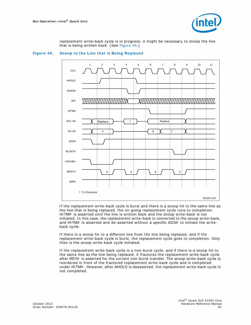
Bus Operation—Intel® Quark Core
replacement write-back cycle is in progress, it might be necessary to snoop the line that is being written back. (See Figure 46.)
Figure 46. Snoop to the Line that is Being Replaced
If the replacement write-back cycle is burst and there is a snoop hit to the same line as the line that is being replaced, the on-going replacement cycle runs to completion. HITM# is asserted until the line is written back and the snoop write-back is not initiated. In this case, the replacement write-back is converted to the snoop write-back, and HITM# is asserted and de-asserted without a specific ADS# to initiate the write-back cycle.
If there is a snoop hit to a different line from the line being replaced, and if the replacement write-back cycle is burst, the replacement cycle goes to completion. Only then is the snoop write-back cycle initiated.
If the replacement write-back cycle is a non-burst cycle, and if there is a snoop hit to the same line as the line being replaced, it fractures the replacement write-back cycle after RDY# is asserted for the current non-burst transfer. The snoop write-back cycle is reordered in front of the fractured replacement write-back cycle and is completed under HITM#. However, after AHOLD is deasserted, the replacement write-back cycle is not completed.
242202-153
CLK
AHOLD
EADS#
INV
HITM#
A31–A4
A3–A2
ADS#
1 2 3 4 5 6 7 8 9 10 11
W/R#
To Processor
BRDY#
CACHE#
BLAST#
0 8 C
Replace
0 4 8 C
Replace
†
†
Intel® Quark SoC X1000 CoreOctober 2013 Hardware Reference ManualOrder Number: 329678-001US 81

Intel® Quark Core—Bus Operation
If there is a snoop hit to a line that is different from the one being replaced, the non-burst replacement write-back cycle is fractured, and the snoop write-back cycle is reordered ahead of the replacement write-back cycle. After the snoop write-back is completed, the replacement write-back cycle continues.
4.4.3.4 Snoop under BOFF#
BOFF# is capable of fracturing any transfer, burst or non-burst. The output pins (see Table 7 and Table 14) of the Write-Back Enhanced Intel® Quark Core are floated in the clock period following the assertion of BOFF#. If the system snoop hits a modified line using BOFF#, the snoop write-back cycle is reordered ahead of the current cycle. BOFF# must be de-asserted for the processor to perform a snoop write-back cycle and resume the fractured cycle. The fractured cycle resumes with a new ADS# and begins with the first uncompleted transfer. Snoops are permitted under BOFF#, but write-back cycles are not started until BOFF# is de-asserted. Consequently, multiple snoop cycles can occur under a continuously asserted BOFF#, but only up to the first asserted HITM#.
Snoop under BOFF# during Cache Line Fill
As shown in Figure 47, BOFF# fractures the second transfer of a non-burst cache line-fill cycle. The system begins snooping by driving EADS# and INV in clock six. The assertion of HITM# in clock eight indicates that the snoop cycle hit a modified line and the cache line is written back to memory. The assertion of HITM# in clock eight and CACHE# and ADS# in clock ten identifies the beginning of the snoop write-back cycle. ADS# is guaranteed to be asserted no sooner than two clock periods after the assertion of HITM#. Write-back cycles always use the four-doubleword address sequence of 0-4-8-C (burst or non-burst). The snoop write-back cycle begins upon the de-assertion of BOFF# with HITM# asserted throughout the duration of the snoop write-back cycle.
If the snoop cycle hits a line that is different from the line being filled, the cache line fill resumes after the snoop write-back cycle completes, as shown in Figure 47.
Intel® Quark SoC X1000 CoreHardware Reference Manual October 201382 Order Number: 329678-001US

Bus Operation—Intel® Quark Core
Figure 47. Snoop under BOFF# during a Cache Line-Fill Cycle
An ADS# is always issued when a cycle resumes after being fractured by BOFF#. The address of the fractured data transfer is reissued under this ADS#, and CACHE# is not issued unless the fractured operation resumes from the first transfer (e.g., first doubleword). If the system asserts BOFF# and RDY# simultaneously, as shown in clock four on Figure 47, BOFF# dominates and RDY# is ignored. Consequently, the Write-Back Enhanced Intel® Quark Core accepts only up to the x4h doubleword, and the line fill resumes with the x0h doubleword. ADS# initiates the resumption of the line-fill operation in clock period 15. HITM# is de-asserted in the clock period following the clock period in which the last RDY# or BRDY# of the write-back cycle is asserted. Hence, HITM# is guaranteed to be de-asserted before the ADS# of the next cycle.
Figure 47 also shows the system asserting RDY# to indicate a non-burst line-fill cycle. Burst cache line-fill cycles behave similarly to non-burst cache line-fill cycles when snooping using BOFF#. If the system snoop hits the same line as the line being filled (burst or non-burst), the Write-Back Enhanced Intel® Quark Core does not assert HITM# and does not issue a snoop write-back cycle, because the line was not modified, and the line fill resumes upon the de-assertion of BOFF#. However, the line fill is cached only if INV is driven low during the snoop cycle.
242202-154
CLK
BOFF#
EADS#
INV
HITM#
ADS#
BLAST#
To Processor
1 2 3 4 5 6 7 8 9 10 11 12 13 14 15 16 17 18 19 20 21 22 23
A31–A4
A3–A2
RDY#
CACHE#
W/R#
BRDY#
Linefill Write Back Cycle Line Fill Cycle Cont.
4 0 0 4 C 8 0 C 8
†
†
Intel® Quark SoC X1000 CoreOctober 2013 Hardware Reference ManualOrder Number: 329678-001US 83

Intel® Quark Core—Bus Operation
Snoop under BOFF# during Replacement Write-Back
If the system snoop under BOFF# hits the line that is currently being replaced (burst or non-burst), the entire line is written back as a snoop write-back line, and the replacement write-back cycle is not continued. However, if the system snoop hits a different line than the one currently being replaced, the replacement write-back cycle continues after the snoop write-back cycle has been completed. Figure 48 shows a system snoop hit to the same line as the one being replaced (non-burst).
Figure 48. Snoop under BOFF# to the Line that is Being Replaced
4.4.3.5 Snoop under HOLD
Note: The implementation of Intel® Quark Core on Intel® Quark SoC X1000 does not support the HOLD mechanism.
HOLD can only fracture a non-cacheable, non-burst code prefetch cycle. For all other cycles, the Write-Back Enhanced Intel® Quark Core does not assert HLDA until the entire current cycle is completed. If the system snoop hits a modified line under HLDA during a non-cacheable, non-burstable code prefetch, the snoop write-back cycle is reordered ahead of the fractured cycle. The fractured non-cacheable, non-burst code prefetch resumes with an ADS# and begins with the first uncompleted transfer. Snoops are permitted under HLDA, but write-back cycles do not occur until HOLD is de-asserted. Consequently, multiple snoop cycles are permitted under a continuously asserted HLDA only up to the first asserted HITM#.
CLK
BOFF#
EADS#
INV
HITM#
A31–A4
A3–A2
ADS#
1 2 3 4 5 6 7 8 9 10 11 12 13 14 15 16 17 18 19
BLAST#
CACHE#
RDY#
BRDY#
To Processor
W/R#
0 4 8 C
Repl Wb
Repl Wb
Write Back Cycle
†
†
Intel® Quark SoC X1000 CoreHardware Reference Manual October 201384 Order Number: 329678-001US
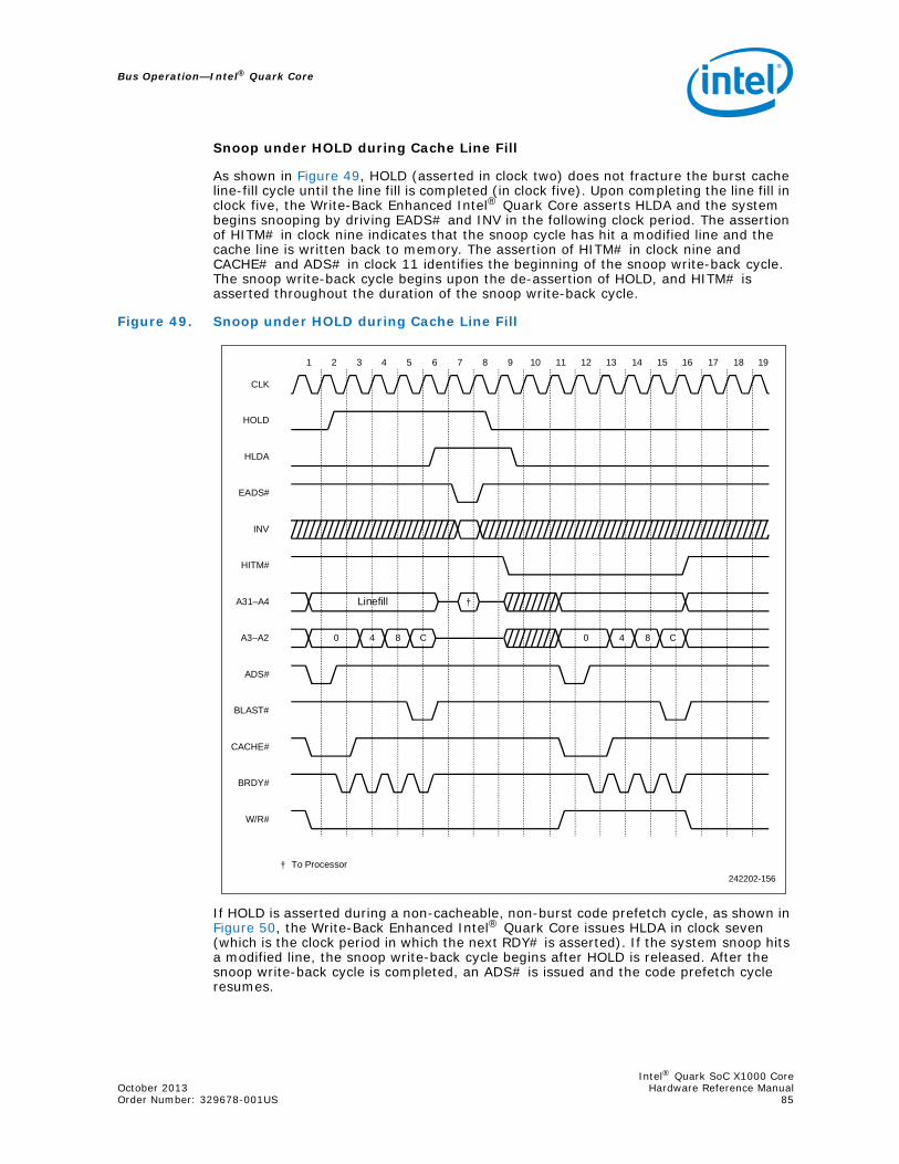
Bus Operation—Intel® Quark Core
Snoop under HOLD during Cache Line Fill
As shown in Figure 49, HOLD (asserted in clock two) does not fracture the burst cache line-fill cycle until the line fill is completed (in clock five). Upon completing the line fill in clock five, the Write-Back Enhanced Intel® Quark Core asserts HLDA and the system begins snooping by driving EADS# and INV in the following clock period. The assertion of HITM# in clock nine indicates that the snoop cycle has hit a modified line and the cache line is written back to memory. The assertion of HITM# in clock nine and CACHE# and ADS# in clock 11 identifies the beginning of the snoop write-back cycle. The snoop write-back cycle begins upon the de-assertion of HOLD, and HITM# is asserted throughout the duration of the snoop write-back cycle.
Figure 49. Snoop under HOLD during Cache Line Fill
If HOLD is asserted during a non-cacheable, non-burst code prefetch cycle, as shown in Figure 50, the Write-Back Enhanced Intel® Quark Core issues HLDA in clock seven (which is the clock period in which the next RDY# is asserted). If the system snoop hits a modified line, the snoop write-back cycle begins after HOLD is released. After the snoop write-back cycle is completed, an ADS# is issued and the code prefetch cycle resumes.
242202-156
CLK
HOLD
HLDA
INV
HITM#
A31–A4
A3–A2
ADS#
1 2 3 4 5 6 7 8 9 10 11 12 13 14 15 16 17 18 19
BLAST#
CACHE#
BRDY#
To Processor
W/R#
0 4 8 C
EADS#
0 4 8 C
Linefill
†
†
Intel® Quark SoC X1000 CoreOctober 2013 Hardware Reference ManualOrder Number: 329678-001US 85

Intel® Quark Core—Bus Operation
Figure 50. Snoop using HOLD during a Non-Cacheable, Non-Burstable Code Prefetch
4.4.3.6 Snoop under HOLD during Replacement Write-Back
Note: The implementation of Intel® Quark Core on Intel® Quark SoC X1000 does not support the HOLD mechanism.
Collision of snoop cycles under a HOLD during the replacement write-back cycle can never occur, because HLDA is asserted only after the replacement write-back cycle (burst or non-burst) is completed.
4.4.4 Locked Cycles
In both Standard and Enhanced Bus modes, the Write-Back Enhanced Intel® Quark Core architecture supports atomic memory access. A programmer can modify the contents of a memory variable and be assured that the variable is not accessed by another bus master between the read of the variable and the update of that variable. This function is provided for instructions that contain a LOCK prefix, and also for
242202-157
CLK
HOLD
EADS#
HITM#
A31–A4
A3–A2
ADS#
1 2 3 4 5 6 7 8 9 10 11 12 13 14 15 16 17 18 19
BLAST#
CACHE#
To Processor
W/R#
0 4 8 C
INV
RDY#
BRDY#
HLDA
C0 4 8
Prefetch Cycle Write Back Cycle PrefetchCont.
†
†
Intel® Quark SoC X1000 CoreHardware Reference Manual October 201386 Order Number: 329678-001US

Bus Operation—Intel® Quark Core
instructions that implicitly perform locked read modify write cycles. In hardware, the LOCK function is implemented through the LOCK# pin, which indicates to the system that the processor is performing this sequence of cycles, and that the processor should be allowed atomic access for the location accessed during the first locked cycle.
A locked operation is a combination of one or more read cycles followed by one or more write cycles with the LOCK# pin asserted. Before a locked read cycle is run, the processor first determines if the corresponding line is in the cache. If the line is present in the cache, and is in an E or S state, it is invalidated. If the line is in the M state, the processor does a write-back and then invalidates the line. A locked cycle to an M, S, or E state line is always forced out to the bus. If the operand is misaligned across cache lines, the processor could potentially run two write back cycles before starting the first locked read. In this case the sequence of bus cycles is: write back, write back, locked read, locked read, locked write and the final locked write. Note that although a total of six cycles are generated, the LOCK# pin is asserted only during the last four cycles, as shown in Figure 51.
LOCK# is not deasserted if AHOLD is asserted in the middle of a locked cycle. LOCK# remains asserted even if there is a snoop write-back during a locked cycle. LOCK# is floated if BOFF# is asserted in the middle of a locked cycle. However, it is driven LOW again when the cycle restarts after BOFF#. Locked read cycles are never transformed into line fills, even if KEN# is asserted. If there are back-to-back locked cycles, the Write-Back Enhanced Intel® Quark Core does not insert a dead clock between these two cycles. HOLD is recognized if there are two back-to-back locked cycles, and LOCK# floats when HLDA is asserted.
Figure 51. Locked Cycles (Back-to-Back)
242202-158
CLK
ADS#
DATA
Ti T1 T2 T1 T2 T1 T2 T1 T2 T1
To ProcessorFrom Processor
RDY#BRDY#
ADDR
CACHE#
LOCK#
W/R#
Rd1 Wt1 Rd2 Wt2
†
‡
‡ † ‡
†
Intel® Quark SoC X1000 CoreOctober 2013 Hardware Reference ManualOrder Number: 329678-001US 87

Intel® Quark Core—Bus Operation
4.4.4.1 Snoop/Lock Collision
If there is a snoop cycle overlaying a locked cycle, the snoop write-back cycle fractures the locked cycle. As shown in Figure 52, after the read portion of the locked cycle is completed, the snoop write-back starts under HITM#. After the write-back is completed, the locked cycle continues. But during all this time (including the write-back cycle), the LOCK# signal remains asserted.
Because HOLD is not acknowledged if LOCK# is asserted, snoop-lock collisions are restricted to AHOLD and BOFF# snooping.
Figure 52. Snoop Cycle Overlaying a Locked Cycle
4.4.5 Flush Operation
The Write-Back Enhanced Intel® Quark Core executes a flush operation when the FLUSH# pin is asserted, and no outstanding bus cycles, such as a line fill or write back, are being processed. In the Enhanced Bus mode, the processor first writes back all the modified lines to external memory. After the write-back is completed, two special cycles are generated, indicating to the external system that the write-back is done. All lines in the internal cache are invalidated after all the write-back cycles are done. Depending on the number of modified lines in the cache, the flush could take a minimum of 1280 bus clocks (2560 processor clocks) and up to a maximum of 5000+ bus clocks to scan the cache, perform the write backs, invalidate the cache, and run the flush acknowledge cycles. FLUSH# is implemented as an interrupt in the Enhanced Bus mode, and is recognized only on an instruction boundary. Write-back system designs should look for the flush acknowledge cycles to recognize the end of the flush operation. Figure 53 shows the flush operation of the Write-Back Enhanced Intel® Quark Core when configured in the Enhanced Bus mode.
242202-159
CLK
ADS#
RDY#BRDY#
AHOLD
ADDR
EADS#
HITM#
W/R#
To ProcessorFrom Processor
1 2 3 4 5 6 7 8 9 10 11 12 13 14 15 16
Write
0 4 8 C
CACHE#
LOCK#
WB1 WB2 WB3 WB4
WriteRead WB
†‡
‡ † ‡
Intel® Quark SoC X1000 CoreHardware Reference Manual October 201388 Order Number: 329678-001US

Bus Operation—Intel® Quark Core
If the Intel® Quark Core is in Standard Bus mode, it does not issue special acknowledge cycles in response to the FLUSH# input, although the internal cache is invalidated. The invalidation of the cache in this case, takes only two bus clocks.
Figure 53. Flush Cycle
4.4.6 Pseudo Locked Cycles
In Enhanced Bus mode, PLOCK# is always deasserted for both burst and non-burst cycles. Hence, it is possible for other bus masters to gain control of the bus during operand transfers that take more than one bus cycle. A 64-bit aligned operand can be read in one burst cycle or two non-burst cycles if BS8# and BS16# are not asserted. Figure 54 shows a 64-bit floating-point operand or Segment Descriptor read cycle, which is burst by the system asserting BRDY#.
4.4.6.1 Snoop under AHOLD during Pseudo-Locked Cycles
AHOLD can fracture a 64-bit transfer if it is a non-burst cycle. If the 64-bit cycle is burst, as shown in Figure 54, the entire transfer goes to completion and only then does the snoop write-back cycle start.
242202-160
CLK
ADS#
RDY#BRDY#
FLUSH#
ADDRM/IO#D/C#
W/R#,BE3–0#
CACHE#
BLAST#
DATA
T1 T1 T2 T2 T2 T2 T1 T1 T2 T1 T2 T1 T1
Write-Back 1st FlushAcknowledge
2nd FlushAcknowledge
Intel® Quark SoC X1000 CoreOctober 2013 Hardware Reference ManualOrder Number: 329678-001US 89

Intel® Quark Core—Bus Operation
Figure 54. Snoop under AHOLD Overlaying Pseudo-Locked Cycle
4.4.6.2 Snoop under Hold during Pseudo-Locked Cycles
As shown in Figure 55, HOLD does not fracture the 64-bit burst transfer. The Write-Back Enhanced Intel® Quark Core does not issue HLDA until clock four. After the 64-bit transfer is completed, the Write-Back Enhanced Intel® Quark Core writes back the modified line to memory (if snoop hits a modified line). If the 64-bit transfer is non-burst, the Write-Back Enhanced Intel® Quark Core can issue HLDA in between bus cycles for a 64-bit transfer.
242202-161
CLK
AHOLD
EADS#
HITM#
A31–A4
A3–A2
ADS#
1 2 3 4 5 6 7 8 9 10 11 12 13 14 15 16 17 18 19
BLAST#
CACHE#
To Processor†
W/R#
0 4 8 C
INV
PLOCK#
BRDY#
Write Back Cycle†
Intel® Quark SoC X1000 CoreHardware Reference Manual October 201390 Order Number: 329678-001US

Bus Operation—Intel® Quark Core
Figure 55. Snoop under HOLD Overlaying Pseudo-Locked Cycle
4.4.6.3 Snoop under BOFF# Overlaying a Pseudo-Locked Cycle
BOFF# is capable of fracturing any bus operation. In Figure 56, BOFF# fractured a current 64-bit read cycle in clock four. If there is a snoop hit under BOFF#, the snoop write-back operation begins after BOFF# is deasserted. The 64-bit write cycle resumes after the snoop write-back operation completes.
242202-162
CLK
HOLD
EADS#
HITM#
A31–A4
A3–A2
ADS#
1 2 3 4 5 6 7 8 9 10 11 12 13 14 15 16 17 18 19
BLAST#
CACHE#
To Processor
W/R#
0 4 8 C
INV
PLOCK#
BRDY#
HLDA
64-BitRead Cycle Write Back Cycle
†
†
Intel® Quark SoC X1000 CoreOctober 2013 Hardware Reference ManualOrder Number: 329678-001US 91

Intel® Quark Core—Bus Operation
Figure 56. Snoop under BOFF# Overlaying a Pseudo-Locked Cycle
CLK
AHOLD
EADS#
HITM#
A31–A4
A3–A2
ADS#
1 2 3 4 5 6 7 8 9 10 11 12 13 14 15 16 17 18 19
BLAST#
CACHE#
To Processor†
W/R#
0 4 8 C
INV
PLOCK#
BRDY#
Write Back Cycle†
242202-163
Intel® Quark SoC X1000 CoreHardware Reference Manual October 201392 Order Number: 329678-001US
Memory Subsystem Design—Intel® Quark Core
5.0 Memory Subsystem Design
5.1 IntroductionThe Intel® Quark Core can access instructions and data from its on-chip cache in the same clock cycle. To support the Intel® Quark Core's internal data path, the external bus has also been optimized. The internal cache requires rapid access to entire cache lines. Invalidation cycles must be supported to maintain consistency with external memory. All of these functions must be supported by the external memory system. Without them, the full performance potential of the CPU cannot be attained.
The requirements of multi-tasking and multiprocessor operating systems also place increased demand on the external memory system. OS support functions such as paging and context switching can degrade reference locality. Without efficient access to external memory, the performance of these functions is degraded.
Second-level (also known as L2) caching is a technique used to improve the memory interface. Some applications, such as multi-user office computers, require this feature to meet performance goals. Single-user systems, on the other hand, may not warrant the extra cost. Due to the variety of applications incorporating the Intel® Quark Core, memory system architecture is very diverse.
Note: The implementation of Intel® Quark Core on Intel® Quark SoC X1000 does not support second-level cache.
5.2 Processor and Cache Feature OverviewThe improvements made to the processor bus interface impact the memory subsystem design. It is important to understand the impact of these features before attempting to define a memory subsystem. This section reviews the bus features that affect the memory interface.
5.2.1 The Burst Cycle
The Intel® Quark Core's burst bus cycle feature has more impact on the memory logic than any other feature. A large portion of the control logic is dedicated to supporting this feature. The L2 cache control is also primarily dedicated to supporting burst cycles.
To understand why the logic is designed this way, we must first understand the function of the burst cycle. Burst cycles are generated by the CPU only when two events occur. First, the CPU must request a cycle which is longer in bytes than the data bus can accommodate. Second, the BRDY# signal must be activated to terminate the cycle. When these two events occur a burst cycle takes place. Note that this cycle occurs regardless of the state of the KEN# input. The KEN# input's function is discussed in the next section.
Intel® Quark SoC X1000 CoreOctober 2013 Hardware Reference ManualOrder Number: 329678-001US 93

Intel® Quark Core—Memory Subsystem Design
With this definition we see that several cases are included as “burstable.” Some examples of burstable cycles are listed in Table 15. These cycle lengths are shown in bytes to clarify the case listed.
The last two cases show that write cycles are burstable. In the last case a write cycle is transferred on an 8- or 16-bit bus. If BRDY# is returned to terminate this cycle, the CPU generates another write cycle without activating ADS#.
Using the burst write feature has debatable performance benefit. Some systems may implement special functions that benefit from the use of burst writes. However, the Intel® Quark Core does not write cache lines. Therefore, all write cycles are 4 bytes long. Most of the devices that use dynamic bus sizing are read-only. This fact further reduces the utility of burst writes.
Note: The implementation of Intel® Quark Core on Intel® Quark SoC X1000 does not support dynamic data bus sizing. Bus width is fixed at 32 bits.
Due to these facts, a memory subsystem design normally does not implement burst write cycles. The BRDY# input is asserted only during main memory read cycles. RDY# is used to terminate all memory write cycles. RDY# is also used for all cycles that are not in the memory subsystem or are not capable of supporting burst cycles. The RDY# input is used, for example, to terminate an EPROM or I/O cycle.
5.2.2 The KEN# Input
The primary purpose of the KEN# input is to determine whether a cycle is to be cached. Only read data and code cycles can be cached. Therefore, these cycles are the only cycles affected by the KEN# input.
Figure 57 shows a typical burst cycle. In this sequence, the value of KEN# is important in two different places. First, to begin a cacheable cycle, KEN# must be active the clock before BRDY# is returned. Second, KEN# is sampled the clock before BLAST# is active. At this time the CPU determines whether this line is written to the cache.
The state of KEN# also determines when read cycles can be burst. Most read cycles are initiated as 4 bytes long from the processor’s cache unit. When KEN# is sampled active, the clock before BRDY# or RDY# is asserted, the cycle is converted to a 16-byte cache line fill by the bus unit. This way, a cycle which would not have been burst can now be burst by activating BRDY#.
Some read cycles can be burst without activating KEN#. The most prevalent example of this type of read cycle is a code fetch. All code fetches are generated as 16-byte cycles from the processor’s cache unit. So, regardless of the state of KEN#, code fetches are always burstable. In addition, several types of data read cycles are generated as 8-byte cycles. These cycles, mentioned previously, are descriptor loads and floating-point operand loads. These cycles can be burst at any time.
The use of the KEN# input affects performance. The design example used in Figure 57 illustrates one way to use this signal effectively.
Table 15. Access Length of Typical CPU Functions
Bus Cycle Size (Bytes)
All code fetches 16
Descriptor loads 8
Cacheable reads 16
Floating-point operand loads 8
Bus size 8 (16) writes 4 (Max)
Intel® Quark SoC X1000 CoreHardware Reference Manual October 201394 Order Number: 329678-001US

Memory Subsystem Design—Intel® Quark Core
Figure 57. Typical Burst Cycle
The primary concern when using KEN# is generating it in time for zero wait state read cycles. Most main memory cycles are zero wait state if an L2 cache is implemented. The access to main memory is one wait state during most read cycles. Any cache access takes place with zero wait states. KEN# must, therefore, be valid during the first T2 of any read cycle.
Once this requirement is established, a problem arises. Decode functions are inherently asynchronous. Therefore, the decoded output that generates KEN# must be synchronized. If it is not, the CPU’s setup and hold times are violated and internal metastability results. With synchronization, the delay required to generate KEN# will be at least three clocks. In the example shown, four clocks are required. In either case the KEN# signal will not be valid before BRDY# is returned for zero or one wait state cycles.
This problem is resolved if KEN# is made active. Figure 58 illustrates this function. In this diagram KEN# is active during the first two clocks of the burst cycle. If this is a data read cycle, KEN# being active at this time causes it to be converted to a 16-byte length. The decode and synchronization of KEN# takes place during the first two T2 states of the cycle. If the cycle turns out to be non-cacheable, KEN# is deactivated in the third T2. Otherwise KEN# is left active and the retrieved data is written to the cache.
BLAST#
KEN#
DATA
BRDY#
T1
A5242-02
T2 T2 T2 T2
Sampledhere
Sampledhere
1 2 3 4
Intel® Quark SoC X1000 CoreOctober 2013 Hardware Reference ManualOrder Number: 329678-001US 95

Intel® Quark Core—Memory Subsystem Design
Figure 58. Burst Cycle: KEN# Normally Active
Some memory devices may be slow enough that 16-byte cycles are undesirable. In this case more than three wait states exist. The KEN# signal can be deactivated prior to returning RDY# or BRDY# if three or more wait states are present. As a result, these slow cycles are not converted to 16-byte cache line fills.
BLAST#
KEN#
DATA
BRDY#
T1
A5243-01
T2 T2 T2 T2
Sampledhere
Sampled here
1 2 3 4
Intel® Quark SoC X1000 CoreHardware Reference Manual October 201396 Order Number: 329678-001US

Cache Subsystem—Intel® Quark Core
6.0 Cache Subsystem
6.1 IntroductionCache is an important means of improving overall system performance. The Intel® Quark Core has an on-chip, unified code and data cache. The on-chip cache is used for both instruction and data accesses and operates on physical addresses. The Intel® Quark Core has a 16-Kbyte cache that is organized in a 4-way set associative manner. To understand cache philosophy and the system advantages of a cache, many issues must be considered.
This chapter discusses the following related cache issues: • Cache theory and the impact of cache on performance. • The relationship between cache size and hit rates when using a first-level cache. • Issues in mapping (or associativity) that arise when main memory is cached.
Different cache configurations including direct-mapped, set associative, and fully associative. They are discussed along with the performance trade-offs inherent to each configuration.
• The impact of cache line sizes and cache re-filling algorithms on performance. • Write-back and write-through methods for updating main memory. How each
method maintain cache consistency and the impact on external bus utilization. • Cache consistency issues that arise when a DMA occurs while the Intel® Quark
Core's cache is enabled. Methods that ensure cache and main memory consistency during cache accesses.
• Cache used in single versus multiple CPU systems.
6.2 Cache MemoryCache memory is high-speed memory that is placed between microprocessors and main memory. Cache memory keeps copies of main memory that are currently in use to speed microprocessor access to requested data and instructions. When properly implemented, cache access time can be three to eight times faster than that of main memory, and thus can reduce the overall access time. Cache also reduces the number of accesses to main memory DRAM, which is important to systems with multiple bus masters that all access that same memory. This section introduces the cache concept and discusses memory performance benefits provided by a cache.
6.2.1 What is a Cache?
A cache memory is a smaller high-speed memory that fits between a CPU and slower main memory. Cache memory is important in increasing computer performance by reducing total memory latency. A cache memory consists of a directory (or tag), and a data memory. Whenever the CPU is required to read or write data, it first accesses the tag memory and determines if a cache hit has occurred, implying that the requested word is present in the cache. If the tags do not match, the data word is not present in the cache. This is called a cache miss. On a cache hit, the cache data memory allows a
Intel® Quark SoC X1000 CoreOctober 2013 Hardware Reference ManualOrder Number: 329678-001US 97

Intel® Quark Core—Cache Subsystem
read operation to be completed more quickly from its faster memory than from a slower main memory access. The hit rate is the percentage of the accesses that are hits, and is affected by the size and organization of the cache, the cache algorithm used, and the program running. An effective cache system maintains data in a way that increases the hit rate. Different cache organizations are discussed later in this chapter. The main advantage of cache is that a larger main memory appears to have the high speed of a cache. For example, a zero-wait state cache that has a hit rate of 90 percent makes main memory appear to be zero-wait state memory for 9 out of 10 accesses.
Programs usually address memory in the neighborhood of recently accessed locations. This is called program locality or locality of reference and it is locality that makes cache systems possible. Code, data character strings, and vectors tend to be sequentially scanned items or items accessed repeatedly, and cache helps the performance in these cases. In some cases the program locality principle does not apply. Jumps in code sequences and context switching are some examples.
6.3 Cache Trade-offsCache efficiency is the cache's ability to keep the code and data most frequently used by the microprocessor. Cache efficiency is measured in terms of the hit rate. Another indication of cache efficiency is system performance; this is the time in which the microprocessor can perform a certain task and is measured in effective bus cycles. An efficient cache reduces external bus cycles and enhances overall system performance. Hit rates are discussed in the next section.
Factors that can affect a cache's performance are: • Size: Increasing the cache size allows more items to be contained in the cache.
Cost is increased, however, and a larger cache cannot operate as quickly as a smaller one.
• Associativity (discussed in Section 6.3, “Cache Trade-offs” on page 98): Increased associativity increases the cache hit rate but also increases its complexity and reduces its speed.
• Line Size: The amount of data the cache must fetch during each cache line replacement (every miss) affects performance. More data takes more time to fill a cache line, but then more data is available and the hit rate increases.
• Write-Back and Write Posting: The ability to write quickly to the cache and have the cache then write to the slower memory increases performance. Implementing these types of cache designs can be very complex, however.
• Features: Adding features such as write-protection (to be able to cache ROM memory), bus watching, and multiprocessing protocols can speed a cache but increases cost and complexity.
• Speed: Not all cache return data to the CPU as quickly as possible. It is less expensive and complex to use slower cache memories and cache logic.
6.3.1 Intel® Quark Core Cache Organization
The Intel® Quark Core's on-board cache is organized 4-way set associative with a line size of 16 bytes. The 16-Kbyte cache is organized as four 4-Kbyte sets. Each 4-Kbyte set is comprised of 256 16-byte lines. Figure 59 shows the cache organization. An application can achieve an extremely high hit rate with the 4-way associativity. The cache is transparent so that the Intel® Quark Core remains software-compatible with its non-cache predecessors.
Intel® Quark SoC X1000 CoreHardware Reference Manual October 201398 Order Number: 329678-001US
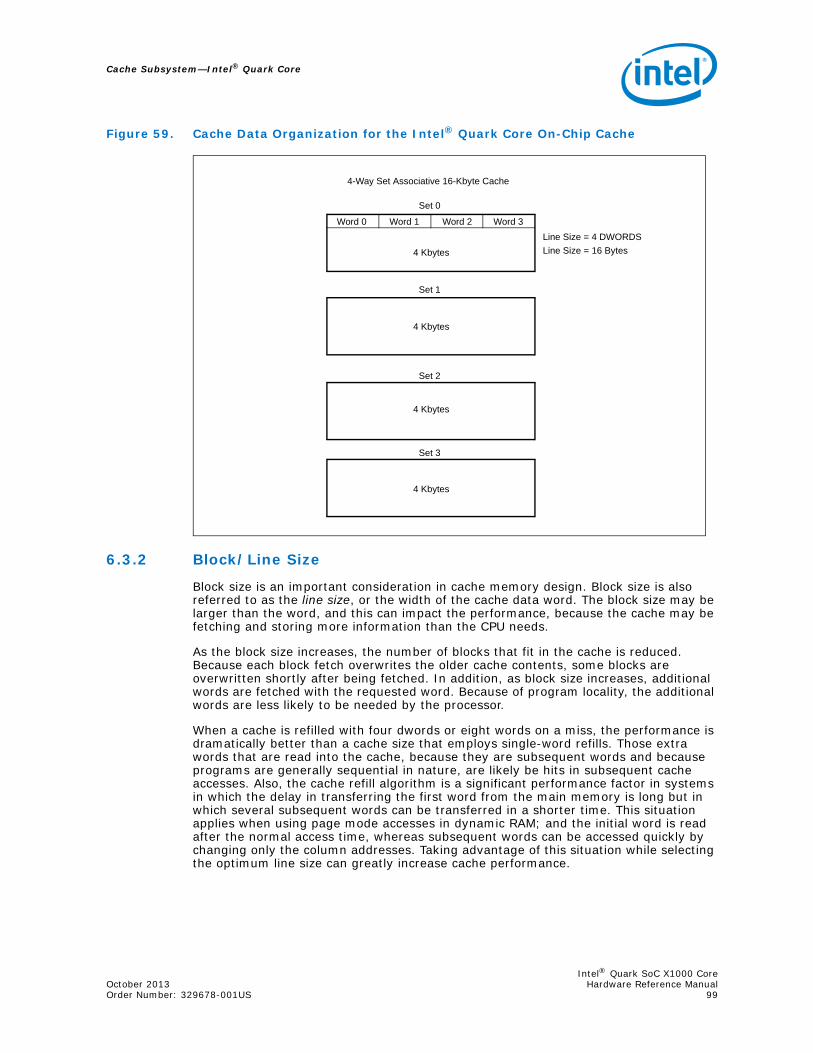
Cache Subsystem—Intel® Quark Core
Figure 59. Cache Data Organization for the Intel® Quark Core On-Chip Cache
6.3.2 Block/Line Size
Block size is an important consideration in cache memory design. Block size is also referred to as the line size, or the width of the cache data word. The block size may be larger than the word, and this can impact the performance, because the cache may be fetching and storing more information than the CPU needs.
As the block size increases, the number of blocks that fit in the cache is reduced. Because each block fetch overwrites the older cache contents, some blocks are overwritten shortly after being fetched. In addition, as block size increases, additional words are fetched with the requested word. Because of program locality, the additional words are less likely to be needed by the processor.
When a cache is refilled with four dwords or eight words on a miss, the performance is dramatically better than a cache size that employs single-word refills. Those extra words that are read into the cache, because they are subsequent words and because programs are generally sequential in nature, are likely be hits in subsequent cache accesses. Also, the cache refill algorithm is a significant performance factor in systems in which the delay in transferring the first word from the main memory is long but in which several subsequent words can be transferred in a shorter time. This situation applies when using page mode accesses in dynamic RAM; and the initial word is read after the normal access time, whereas subsequent words can be accessed quickly by changing only the column addresses. Taking advantage of this situation while selecting the optimum line size can greatly increase cache performance.
Word 0 Word 1 Word 2 Word 3
4 Kbytes
Set 0
Set 1
Set 2
Set 3
4 Kbytes
4 Kbytes
4 Kbytes
4-Way Set Associative 16-Kbyte Cache
Line Size = 4 DWORDS
Line Size = 16 Bytes
Intel® Quark SoC X1000 CoreOctober 2013 Hardware Reference ManualOrder Number: 329678-001US 99
Intel® Quark Core—Cache Subsystem
6.3.3 Replacement Policy
In a set-associative cache configuration, a replacement policy is needed to determine which set should receive new data when the cache is updated. There are four common approaches for choosing which block (or single word) within a set is be overwritten. These are the least recently used (LRU) method, the pseudo LRU method, the first-in first-out (FIFO) method, and the random method.
In the LRU method, the set that was least recently accessed is overwritten. The control logic must maintain least recently used bits and must examine the bits before an update occurs. In the pseudo LRU method, the set that was assumed to be the least recently accessed is overwritten. In the FIFO method, the cache overwrites the block that is resident for the longest time. In the random method, the cache arbitrarily replaces a block. The performance of the algorithms depends on the program behavior. The LRU method is preferred because it provides the best hit rate.
6.4 Updating Main MemoryWhen the processor executes instructions that modify the contents of the cache, changes have to be made in the main memory as well; otherwise, the cache is only a temporary buffer and it is possible for data inconsistencies to arise between the main memory and the cache. If only one of the cache or the main memory is altered and the other is not, two different sets of data become associated with the same address.
There are two general approaches to updating the main memory. The first is the write-through method; and the second is the write-back, also known as copy-back method. Memory traffic issues are discussed for both methods.
6.4.1 Write-Through and Buffered Write-Through Systems
In a write-through system, data is written to the main memory immediately after or while it is written into the cache. As a result, the main memory always contains valid data. The advantage to this approach is that any block in the cache can be overwritten without data loss, while the hardware implementation remains fairly straightforward. There is a memory traffic trade-off, however, because every write cycle increases the bus traffic on a slower memory bus. This can create contention for use of the memory bus by other bus masters. Even in a buffered write-through scheme, each write eventually goes to memory. Thus, bus utilization for write cycles is not reduced by using a write-through or buffered write-through cache.
Users sometimes adopt a buffered write-through approach in which the write accesses to the main memory can be buffered with a N-deep pipeline. A number of words are stored in pipelined registers, and will subsequently be written to the main memory. The processor can begin a new operation before the write operation to main memory is completed. If a read access follows a write access, and a cache hit occurs, then data can be accessed from the cache memory while the main memory is updated. When the N-deep pipeline is full, the processor must wait if another write access occurs and the main memory has not yet been updated. A write access followed by a read miss also requires the processor to wait because the main memory has to be updated before the next read access.
Pipeline configurations must account for multiprocessor complications when another processor accesses a shared main memory location which has not been updated by the pipeline. This means the main memory hasn't been updated, and the memory controller must take the appropriate action to prevent data inconsistencies.
Intel® Quark SoC X1000 CoreHardware Reference Manual October 2013100 Order Number: 329678-001US

Cache Subsystem—Intel® Quark Core
6.4.2 Write-Back System
In a write-back system, the processor writes data into the cache and sets a “dirty bit” which indicates that a word had been written into the cache but not into the main memory. The cache data is written into the main memory at a later time and the dirty bit is cleared. Before overwriting any word or block in the cache, the cache controller looks for a dirty bit and updates the main memory before loading the cache with the new data.
A write-back cache accesses memory less often than a write-through cache because the number of times that the main memory must be updated with altered cache locations is usually lower than the number of write accesses. This results in reduced traffic on the main memory bus.
A write-back cache can offer higher performance than a write-through cache if writes to main memory are slow. The primary use of the a write-back cache is in a multiprocessing environment. Since many processors must share the main memory, a write-back cache may be required to limit each processor's bus activity, and thus reduce accesses to main memory. It has been shown that in a single-CPU environment with up to four clock memory writes, there is no significant performance difference between a write-through and write-back cache.
There are some disadvantages to a write-back system. The cache control logic is more complex because addresses have to be reconstructed from the tag RAM and the main memory has to be updated along with the pending request. For DMA and multiprocessor operations, all locations with an asserted dirty bit must be written to the main memory before another device can access the corresponding main memory locations.
6.4.3 Cache Consistency
Write-through and write-back systems require mechanisms to eliminate the problem of stale main memory in a multiprocessing system or in a system with a DMA controller. If the main memory is updated by one processor, the cache data maintained by another processor may contain stale data. A system that prevents the stale data problem is said to maintain cache consistency. There are four methods commonly used to maintain cache consistency: snooping (or bus watching), broadcasting (or hardware transparency), non-cacheable memory designation, and cache flushing.
In snooping, cache controllers monitor the bus lines and invalidate any shared locations that are written by another processor. The common cache location is invalidated and cache consistency is maintained. This method is shown in Figure 60.
Intel® Quark SoC X1000 CoreOctober 2013 Hardware Reference ManualOrder Number: 329678-001US 101

Intel® Quark Core—Cache Subsystem
Figure 60. Bus Watching/Snooping for Shared Memory Systems
In broadcasting/hardware transparency, the addresses of all stores are transmitted to all the other cache so that all copies are updated. This is accomplished by routing the accesses of all devices to main memory through the same cache. Another method is by copying all cache writes to main memory and to all of the cache that share main memory. A hardware transparent system is shown in Figure 61.
Figure 61. Hardware Transparency
In non-cacheable memory systems, all shared memory locations are considered non-cacheable. In such systems, access to the shared memory is never copied in the cache, and the cache never receives stale data. This can be implemented with chip select logic or with the high order address bits. Figure 62 shows non-cacheable memory.
SharedMemory
CacheController
SnoopAddress I/P
OtherBus Master(s)
CPU
MainMemory
Cache
CacheCPU
OtherBus
Master
Intel® Quark SoC X1000 CoreHardware Reference Manual October 2013102 Order Number: 329678-001US

Cache Subsystem—Intel® Quark Core
Figure 62. Non-Cacheable Share Memory
In cache flushing, all cache locations with set dirty bits are written to main memory (for write-back systems), then cache contents are cleared. If all of the devices are flushed before another bus master writes to shared memory, cache consistency is maintained.
Combinations of various cache coherency techniques may be used in a system to provide an optimal solution. A system may use hardware transparency for time critical I/O operations such as paging, and it may partition the memory as non-cacheable for slower I/O operations such as printing.
6.5 Non-Cacheable Memory Locations To avoid cache consistency problems, certain memory locations must not be cached. The PC architecture has several special memory areas which may not be cached. If ROM locations on add-in cards are cached, for example, write operations to the ROM can alter the cache while main memory contents remain the same. Further, if the mode of a video RAM subsystem is switched, it can produce altered versions of the original data when a read-back is performed. Expanded memory cards may change their mapping, and hence memory contents, with an I/O write operation. LAN or disk controllers with local memory may change the memory contents independent of the Intel® Quark Core. This altering of certain memory locations can cause a cache consistency problem. For these reasons, the video RAM, shadowed BIOSROMs, expanded memory boards, add-in cards, and shadowed expansion ROMs should be non-cacheable locations. Depending on the system design, ROM locations may be cacheable in a second-level cache if write protection is allowed.
Note: The implementation of Intel® Quark Core on Intel® Quark SoC X1000 does not support second-level cache.
6.6 Cache and DMA OperationsSome of the issues related to cache consistency in systems employing DMA have already been covered in the preceding section. Because a DMA controller or other bus master can update main memory, there is a possibility of stale data in the cache. The problem can be avoided through snooping, cache transparency, and non-cacheable designs.
CPU Decoder
OtherBus
Master
Cache
Non-cacheable
Cacheable
Intel® Quark SoC X1000 CoreOctober 2013 Hardware Reference ManualOrder Number: 329678-001US 103

Intel® Quark Core—Cache Subsystem
In snooping, the cache controller monitors the system address bus and invalidates cache locations that will be written to during a DMA cycle. This method is advantageous in that the processor can access its cache during DMA operations to main memory. Only a “snoop hit” causes an invalidation cycle (or update cycle) to occur.
In cache transparency, memory accesses through the CPU and the DMA controller are directed through the cache, requiring minimal hardware. However, the main disadvantage is that while a DMA operation is in progress, the CPU bus is placed in HOLD. The concurrency of CPU/cache and DMA controller/main memory operations is not supported.
In non-cacheable designs, a separate dual-ported memory can be used as the non-cacheable portion of the memory, and the DMA device is tightly coupled to this memory. In this way, the problem of stale data cannot occur.
In all of the approaches, the cache should be made software transparent so that DMA cycles do not require special software programming to ensure cache coherency.
Intel® Quark SoC X1000 CoreHardware Reference Manual October 2013104 Order Number: 329678-001US

Peripheral Subsystem—Intel® Quark Core
7.0 Peripheral Subsystem
The peripheral (I/O) interface is an essential part of any embedded processor system. It supports communications between the microprocessor and the peripherals. Given the variety of existing peripheral devices, a peripheral system must allow a variety of interfaces. An important part of a microprocessor system is the bus that connects all major parts of the system. This chapter describes the connection of peripheral devices to the Intel® Quark Core bus. This chapter presents design techniques for interfacing different devices with the Intel® Quark Core, such as LAN controllers and EISA, VESA local bus, and PCI chip sets.
The peripheral subsystem must provide sufficient data bandwidth to support the Intel® Quark Core. High-speed devices like disks must be able to transfer data to memory with minimal CPU overhead or interaction. The on-chip cache of the Intel® Quark Core requires further considerations to avoid stale data problems. These subjects are also covered in this chapter.
The Intel® Quark Core supports 8-bit, 16-bit and 32-bit I/O devices, which can be I/O-mapped, memory-mapped, or both. It has a 106 Mbyte/sec memory bandwidth at 33 MHz. Cache coherency is supported by cache line invalidation and cache flush cycles. I/O devices can be accessed by dedicated I/O instructions for I/O-mapped devices, or by memory operand instructions for memory-mapped devices. In addition, the Intel® Quark Core always synchronizes I/O instruction execution with external bus activity. All previous instructions are completed before an I/O operation begins. In particular, all writes pending in the write buffers are completed before an I/O read or write is performed. These functions are described in this chapter.
Note: The implementation of Intel® Quark Core on Intel® Quark SoC X1000 does not support dynamic data bus sizing. Bus width is fixed at 32 bits.
7.1 Peripheral/Processor Bus InterfaceBecause the Intel® Quark Core supports both memory-mapped and I/O-mapped devices, this section discusses the types of mapping, support for dynamic bus sizing, byte swap logic, and critical timings. An example of a basic I/O controller implementation is also included. Some system-oriented interface considerations are discussed because they can have a significant influence on overall system performance.
Note: The implementation of Intel® Quark Core on Intel® Quark SoC X1000 does not support dynamic bus sizing.
7.1.1 Mapping Techniques
The system designer should have a thorough understanding of the system application and its use of peripherals in order to design the optional mapping scheme. Two techniques can be used to control the transmission of data between the computer and its peripherals. The most straightforward approach is I/O mapping.
Intel® Quark SoC X1000 CoreOctober 2013 Hardware Reference ManualOrder Number: 329678-001US 105

Intel® Quark Core—Peripheral Subsystem
The Intel® Quark Core can interface with 8-bit, 16-bit or 32-bit I/O devices, which can be I/O-mapped, memory-mapped, or both. All I/O devices can be mapped into physical memory addresses ranging from 00000000H to FFFFFFFFH (four-gigabytes) or I/O addresses ranging from 00000000H to 0000FFFFH (64 Kbytes) for programmed I/O, as shown in Figure 63.
Note: The implementation of Intel® Quark Core on Intel® Quark SoC X1000 supports 32-bit devices only.
Figure 63. Mapping Scheme
I/O mapping and memory-mapping differ in the following respects:• The address decoding required to generate chip selects for the I/O-mapped devices
is much simpler than that required for memory-mapped devices. I/O-mapped devices reside within the I/O space of the Intel® Quark Core (64 Kbytes); memory-mapped devices reside in a much larger Intel® Quark Core memory space (4-gigabytes), which requires more address lines to decode.
• The I/O space is 64 Kbytes and can be divided into 64 K of 8-bit ports, 32 K of 16-bit ports, 16 K of 32-bit ports or any combinations of ports which add up to less than 64 Kbytes. The 64 Kbytes of I/O address space refers to physical memory because I/O instructions do not utilize the segmentation or paging hardware and are directly addressable using DX registers.
• Memory-mapped devices can be accessed using the Intel® Quark Core's instructions, so that I/O to memory, memory-to-I/O, and I/O-to-I/O transfers, as well as compare and test operations, can be coded efficiently.
• The I/O-mapped device can be accessed only with IN, OUT, INS, and OUTS instructions. I/O instruction execution is synchronized with external bus activity. All I/O transfers are performed using the AL (8-bit), AX (16-bit), or EAX (32-bit) registers.
• Memory mapping offers more flexibility in Protected Mode than I/O mapping. Memory-mapped devices are protected by the memory management and protection features. A device can be inaccessible to a task, visible but protected, or
PhysicalMemory
NotAccessible
NotAccessible
64 Kbyte
FFFFFFFFH
00000000H
0000FFFFH
00000000H
AccessibleProgrammedI/O Space
I/O SpacePhysical MemorySpace
4 Gbyte
Intel® Quark SoC X1000 CoreHardware Reference Manual October 2013106 Order Number: 329678-001US

Peripheral Subsystem—Intel® Quark Core
fully accessible, depending on where it is mapped. Paging and segmentation provide the same protection levels for 4-Kbyte pages or variable length segments, which can be swapped to the disk or shared between programs. The Intel® Quark Core supports pages and segments to provide the designer with maximum flexibility.
• The I/O privilege level of the Intel® Quark Core protects I/O-mapped devices by either preventing a task from accessing any I/O devices or by allowing a task to access all I/O devices. A virtual-8086 mode I/O permission bitmap can be used to select the privilege level for a combination of I/O bytes.
7.1.2 Dynamic Data Bus Sizing
Note: The implementation of Intel® Quark Core on Intel® Quark SoC X1000 does not support dynamic data bus sizing.
Dynamic data bus sizing allows a direct processor connection to 32-, 16- or 8-bit buses for memory or I/O devices. The Intel® Quark Core supports dynamic data bus sizing. With dynamic bus sizing, the bus width is determined during each bus cycle to accommodate data transfers to or from 32-bit, 16-bit or 8-bit devices. The decoding circuitry can assert BS16# for 16-bit devices, or BS8# for 8-bit devices for each bus cycle. For addressing 32-bit devices, both BS16# and BS8# are deasserted. If both BS16# and BS8# are asserted, an 8-bit bus width is assumed.
Appropriate selection of BS16# and BS8# drives the Intel® Quark Core to run additional bus cycles to complete requests larger than 16-bits or 8-bits. When BS16# is asserted, a 32-bit transfer is converted into two 16-bit transfers (or three transfers if the data is misaligned). Similarly, asserting BS8# converts 32-bit transfers into four 8-bit transfers. The extra cycles forced by the BS16# or BS8# signals should be viewed as independent cycles. BS16# or BS8# are normally driven active during the independent cycles. The only exception is when the addressed device can vary the number of bytes that it can return between the cycles.
The Intel® Quark Core drives the appropriate byte enables during the independent cycles initiated by BS8# and BS16#. Addresses A31–A2 do not change if accesses are to a 32-bit aligned area. Table 16 shows the set of byte enables that is generated on the next cycle for each of the valid possibilities of the byte enables on the current cycle. BEx# must be ignored for 16-byte cycles to memory-mapped devices.
Table 16. Next Byte-Enable Values for the BSx# Cycles
Current Next with BS8# Next with BS16#
BE3# BE2# BE1# BE0# BE3# BE2# BE1# BE0# BE3# BE2# BE1# BE0#
1 1 1 0 N N N N N N N N
1 1 0 0 1 1 0 1 N N N N
1 0 0 0 1 0 0 1 1 0 1 1
0 0 0 0 0 0 0 1 0 0 1 1
1 1 0 1 N N N N N N N N
1 0 0 1 1 0 1 1 1 0 1 1
0 0 0 1 0 0 1 1 0 0 1 1
1 0 1 1 N N N N N N N N
0 0 1 1 0 1 1 1 N N N N
0 1 1 1 N N N N N N N N
Note: “N” means that another bus cycle is not required to satisfy the request.
Intel® Quark SoC X1000 CoreOctober 2013 Hardware Reference ManualOrder Number: 329678-001US 107
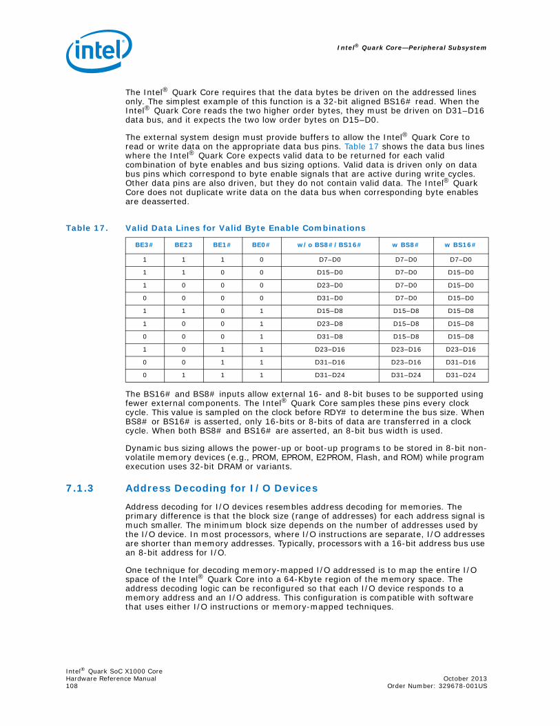
Intel® Quark Core—Peripheral Subsystem
The Intel® Quark Core requires that the data bytes be driven on the addressed lines only. The simplest example of this function is a 32-bit aligned BS16# read. When the Intel® Quark Core reads the two higher order bytes, they must be driven on D31–D16 data bus, and it expects the two low order bytes on D15–D0.
The external system design must provide buffers to allow the Intel® Quark Core to read or write data on the appropriate data bus pins. Table 17 shows the data bus lines where the Intel® Quark Core expects valid data to be returned for each valid combination of byte enables and bus sizing options. Valid data is driven only on data bus pins which correspond to byte enable signals that are active during write cycles. Other data pins are also driven, but they do not contain valid data. The Intel® Quark Core does not duplicate write data on the data bus when corresponding byte enables are deasserted.
The BS16# and BS8# inputs allow external 16- and 8-bit buses to be supported using fewer external components. The Intel® Quark Core samples these pins every clock cycle. This value is sampled on the clock before RDY# to determine the bus size. When BS8# or BS16# is asserted, only 16-bits or 8-bits of data are transferred in a clock cycle. When both BS8# and BS16# are asserted, an 8-bit bus width is used.
Dynamic bus sizing allows the power-up or boot-up programs to be stored in 8-bit non-volatile memory devices (e.g., PROM, EPROM, E2PROM, Flash, and ROM) while program execution uses 32-bit DRAM or variants.
7.1.3 Address Decoding for I/O Devices
Address decoding for I/O devices resembles address decoding for memories. The primary difference is that the block size (range of addresses) for each address signal is much smaller. The minimum block size depends on the number of addresses used by the I/O device. In most processors, where I/O instructions are separate, I/O addresses are shorter than memory addresses. Typically, processors with a 16-bit address bus use an 8-bit address for I/O.
One technique for decoding memory-mapped I/O addressed is to map the entire I/O space of the Intel® Quark Core into a 64-Kbyte region of the memory space. The address decoding logic can be reconfigured so that each I/O device responds to a memory address and an I/O address. This configuration is compatible with software that uses either I/O instructions or memory-mapped techniques.
Table 17. Valid Data Lines for Valid Byte Enable Combinations
BE3# BE23 BE1# BE0# w/o BS8#/BS16# w BS8# w BS16#
1 1 1 0 D7–D0 D7–D0 D7–D0
1 1 0 0 D15–D0 D7–D0 D15–D0
1 0 0 0 D23–D0 D7–D0 D15–D0
0 0 0 0 D31–D0 D7–D0 D15–D0
1 1 0 1 D15–D8 D15–D8 D15–D8
1 0 0 1 D23–D8 D15–D8 D15–D8
0 0 0 1 D31–D8 D15–D8 D15–D8
1 0 1 1 D23–D16 D23–D16 D23–D16
0 0 1 1 D31–D16 D23–D16 D31–D16
0 1 1 1 D31–D24 D31–D24 D31–D24
Intel® Quark SoC X1000 CoreHardware Reference Manual October 2013108 Order Number: 329678-001US

Peripheral Subsystem—Intel® Quark Core
Addresses can be assigned arbitrarily within the I/O or memory space. Addresses for either I/O-mapped or memory-mapped devices should be selected so as to minimize the number of address lines needed.
7.1.3.1 Address Bus Interface
Figure 64 shows the Intel® Quark Core address interface to 32-bit devices.
Figure 64. Intel® Quark Core Interface to I/O Devices
7.1.3.2 32-Bit I/O Interface
A simple 32-bit I/O interface is shown in Figure 65. The example uses only four 8-bit wide bidirectional buffers which are enabled by BE3#–BE0#. Table 17 provides different combinations of BE3#–BE0#. To provide greater flexibility in I/O interface implementation, the design should include interfaces for 32-, 16- and 8-bit devices. The truth table for a 32-to-32-bit interface is shown in Table 18.
Address Bus(A31–A2, BE3#–BE0#)
32-BitI/O
Devices
16-BitI/O
Devices
8-BitI/O
Devices
A31–A2
BE3#–BE0#
ByteSelect
BHE#,BLE#,A1
A0(BLE#), A1AddressDecoder
BS8# BS16#BS8# = BS16# = HIGHfor 32-Bit Addressing
A31–A2
Processor
Intel® Quark SoC X1000 CoreOctober 2013 Hardware Reference ManualOrder Number: 329678-001US 109

Intel® Quark Core—Peripheral Subsystem
Figure 65. 32-Bit I/O Interface
BUFF 0
BUFF 1
BUFF 2
BUFF 3
BE3#
8
8
8
8
8
8
8
8
BE2#
BE1#
BE0#
Intel® Quark Core Processor Data Bus 32-Bit I/O Device
Table 18. 32-Bit to 32-Bit Bus Swapping Logic Truth Table (Sheet 1 of 2)
Intel® Quark Core 8-Bit Interface(1)
BE3# BE2# BE1# BE0# BEN16# BEN8UH# BEN8UL# BEN8H# BHE#(2) A1 A0
0 0 0 0 1 1 1 1 X X X
1 0 0 0 1 1 1 1 X X X
0 1 0 0(3) 1 1 1 1 X X X
1 1 0 0 1 1 1 1 X X X
0 0 1 0(3) 1 1 1 1 X X X
1 0 1 0(3) 1 1 1 1 X X X
0 1 1 0(3) 1 1 1 1 X X X
1 1 1 0 1 1 1 1 X X X
0 0 0 1 1 1 1 1 X X X
Intel® Quark SoC X1000 CoreHardware Reference Manual October 2013110 Order Number: 329678-001US

Peripheral Subsystem—Intel® Quark Core
7.2 Basic Peripheral SubsystemAll microprocessor systems include a CPU, memory and I/O devices which are linked by the address, data and control buses. Figure 66 illustrates the system block diagram of a typical Intel® Quark Core-based system.
1 0 0 1 1 1 1 1 X X X
0 1 0 1(3) 1 1 1 1 X X X
1 1 0 1 1 1 1 1 X X X
0 0 1 1 1 1 1 1 X X X
1 0 1 1 1 1 1 1 X X X
0 1 1 1 1 1 1 1 X X X
1 1 1 1(3) 1 1 1 1 X X X
Inputs Outputs
Notes:1. X implies “do not care” (either 0 or 1).2. BHE# (byte high enable) is not needed in 8-bit interface.3. Indicates a non-occurring pattern of byte enables; either none are asserted or the pattern has byte
enables asserted for non-contiguous bytes.
Table 18. 32-Bit to 32-Bit Bus Swapping Logic Truth Table (Sheet 2 of 2)
Intel® Quark Core 8-Bit Interface(1)
BE3# BE2# BE1# BE0# BEN16# BEN8UH# BEN8UL# BEN8H# BHE#(2) A1 A0
Intel® Quark SoC X1000 CoreOctober 2013 Hardware Reference ManualOrder Number: 329678-001US 111

Intel® Quark Core—Peripheral Subsystem
Figure 66. System Block Diagram
An embedded Intel® Quark Core system may consist of several subsystems. The heart of the system is the processor. The memory subsystem is also important and must be efficient and optimized to provide peak system level performance. As described in Chapter 5.0, “Memory Subsystem Design” it is necessary to utilize the burst-bus feature of the Intel® Quark Core for the DRAM control implementation. The cache subsystem, as described in Chapter 6.0, “Cache Subsystem” also plays an important role in overall system performance. For many systems however, the on-chip cache provides sufficient performance.
A high-performance Intel® Quark Core-based system, requires an efficient peripheral subsystem. This section describes the elements of this system, including the I/O devices on the expansion bus (the memory bus) and the local I/O bus. In a typical system, a number of slave I/O devices can be controlled through the same local bus interface. Complex peripheral devices which can act as bus masters may require a more complex interface.
The bus interface control logic is shown in Figure 67 and consists of three main blocks: the bus control and ready logic, the data transceiver and byte swap logic, and the address decoder.
Processor
LANController
CacheSubsystem
MemorySubsystems
DMAC
Memory Bus
BusTranslator
I/O Bus
BusInterface
SCSI/IPIInterface
ESDI
(EISA, MCA,
Proprietary)PCI, ISA, or
Intel® Quark SoC X1000 CoreHardware Reference Manual October 2013112 Order Number: 329678-001US

Peripheral Subsystem—Intel® Quark Core
Figure 67. Basic I/O Interface Block Diagram
7.2.1 Bus Control and Ready Logic
A typical peripheral device has address inputs which the processor uses to select the device's internal registers. It also has a chip select (CS#) signal which enables it to read data from and write data to the data bus, as controlled by the READ (RD#) and WRITE (WR#) control signals. For a processor that has separate memory and I/O addressing, either memory or I/O read and write signals can be used. As discussed in Section 7.1.1, “Mapping Techniques” on page 105, when memory read and write signals are used to access the peripheral device, the device is called a memory-mapped I/O device.
Many peripheral devices also generate an interrupt output which is asserted when a response is required from the processor. Here, the processor must generate an interrupt acknowledge (INTA#) signal.
Clock CLK
ADS#
M/IO#
D/C#
W/R#
RDY#
ADS#
M/IO#
D/C#
W/R#
RDY#
CPU
Bus Controland Ready
IOCYC
EN
AddressDecoder
CS1#
CS0#
INTA
RECOV
IOR#
IOW#
CS0#
CS1#
OE#Data
Transceiver
DIR DataBus
CS0#RD#
WR#
A2
I/O #2(32-Bit)
I/O #1(32-Bit)
RD#
WR#
A2
CS1#
32
32 32 4
(To Interrupt Controller)
DataBus
AddrBus
BE3#–BE0#
Intel® Quark SoC X1000 CoreOctober 2013 Hardware Reference ManualOrder Number: 329678-001US 113

Intel® Quark Core—Peripheral Subsystem
The bus controller decodes the Intel® Quark Core’s status outputs (W/R#, M/IO# and D/C#) and activates command signals according to the type of bus cycle requested.
The bus controller can be used to do the following:1. Generate an EPROM data read when the control logic generates a signal such as a
memory read command (EPRD#). The command forces the selected memory device to output data.
2. Generate the IOCYC# signal which indicates to the address decoder that a valid I/O cycle is taking place. As a result, the relevant chip select (CS#) signal should be enabled for the I/O device. Once IOCYC is generated, the IOR# and IOW# signals are asserted according to the decoded Intel® Quark Core status signals (explained later).
3. Initiate I/O read cycles when W/R# is low and M/IO# is low. The I/O read command (IOR#) is generated. IOR# selects the I/O device which is to output the data.
4. Initiate an I/O write cycle when W/R# is high and M/IO# is low. The I/O write command signal (IOW#) is generated. This signal instructs a selected I/O device to receive data from the Intel® Quark Core.
5. Generate a RECOV signal which is used for recovery and to avoid data contention. This signal is detailed in Section 7.2.5, “Recovery and Bus Contention” on page 119.
6. Generates the interrupt acknowledge signal (INTA#). This signal is sent to the 82C59A programmable interrupt controller to enable 82C59A interrupt vector data onto the Intel® Quark Core data bus using a sequence of interrupt acknowledge pulses that are issued by the control logic.
7.2.2 Bus Control Signal Description
The following list describes the input/output signals for the bus control logic.
7.2.2.1 Intel® Quark Core Interface
ADS#—Address Status. This input signal to the bus controller is connected directly to the Intel® Quark Core ADS# output. It indicates that a valid bus cycle definition and address are available on the cycle definition lines and address bus. ADS# is driven active at the same time when addresses are driven.
M/IO#—Memory/Input-Output Signal D/C#—Data/Control W/R#—Write/Read (Input signals to bus controller)
These signals are connected directly to the Intel® Quark Core's bus cycle status outputs. For the Intel® Quark Core, they are valid when ADS# is asserted. Table 19 describes the bus cycles of various combinations of M/IO#, D/C# and W/R# signals.
Table 19. Bus Cycle Definitions (Sheet 1 of 2)
M/IO# D/C# W/R# ADS# Bus Cycle Initiated
0 0 0 0 Interrupt acknowledge
0 0 1 0 Halt/special cycle
0 1 0 0 I/O read
0 1 1 0 I/O write
Note: † Intel reserved. Do not use.
Intel® Quark SoC X1000 CoreHardware Reference Manual October 2013114 Order Number: 329678-001US

Peripheral Subsystem—Intel® Quark Core
RDY#—Ready Output Signal. This signal is connected directly to the Intel® Quark Core's RDY# input and indicates that the current bus cycle is complete. It also indicates that the I/O device has returned valid data to the Intel® Quark Core's data pins following an I/O write cycle. For the Intel® Quark Core, RDY# is ignored when the bus is idle and at the end of the first clock of the bus cycle. The signal is utilized in wait state generation which is covered in the next section.
CLK#—Clock Input Signal. This signal provides the fundamental timings for the bus control logic and is synchronous with the processor's clock. All of the external timings are specified with respect to the rising edge of the clock.
7.2.3 Wait State Generator Logic
When the memory subsystem or the I/O device cannot respond to the processor in time, wait states are added to the bus cycles. During wait states the processor freezes the state of the bus. On the Intel® Quark Core, wait states are activated by the RDY# signal (when asserted). Additional wait states are generated as long as RDY# stays deasserted, and the processor resumes its operations once RDY# is asserted.
Timing differences between microprocessors and peripheral devices are common, but can be compensated for by using wait states or some other delay techniques. The following major timing parameters must be accounted for:1. Minimum pulse width for read and write timings2. Chip select access time3. Address access time4. Access time from read strobe
It is possible to adjust the minimum pulse width and chip select access time by adding wait states. Refer to Chapter 4.0, “Bus Operation” for more detailed information on adding wait states to basic bus cycles.
Figure 68 shows PLD equations for basic I/O control logic. A wait state generator should be implemented to optimize wait state generation.
1 0 0 0 Code read
1 0 1 0 Reserved†
1 1 0 0 Memory read
1 1 1 0 Memory write
Table 19. Bus Cycle Definitions (Sheet 2 of 2)
M/IO# D/C# W/R# ADS# Bus Cycle Initiated
Note: † Intel reserved. Do not use.
Intel® Quark SoC X1000 CoreOctober 2013 Hardware Reference ManualOrder Number: 329678-001US 115

Intel® Quark Core—Peripheral Subsystem
Figure 68. PLD Equations for Basic I/O Control Logic
The equation in Figure 68 shows an implementation of a seven-state wait state controller. The wait state logic inserts the needed wait states according to the number required by the device being accessed. In a simple design, I/O accesses can be designated as being equal to the number of wait states required by the slowest device.
7.2.4 Address Decoder
The function of the address decoder is to decode the most significant address bits and generate address select signals for each system device. The address space is divided into blocks, and the address select signals indicate whether the address on the address bus is within the predetermined range. The block size usually represents the amount of address space that can be accessed within a particular device and the address select signal is asserted for any address within that range.
Address select signals are asserted within the range of addresses which is determined by the decoded address lines. The relationship between memory and I/O mapping and address decoding is given by the following equation: Given that n = bits to decoder
m = bits to I/O or memory then # of chip selects = 2n
address range = 2m = # of least significant address lines
For example, when the address decoder decodes A13 through the most significant address bits, the least significant 13 address bits A2 to A12 are ignored. Hence the address select can be asserted for a 2-Kbyte address range.
For I/O-mapped devices, the maximum I/O space is 64 Kbytes. When using I/O instructions the block size (range of addresses) for each address select signal is much smaller than the address space of the memory-mapped devices. The minimum block size is determined according to the number of addresses being used by the peripheral device.
Inputs ADS#, M/IO#, D/C#, W/R#, SEL0, SEL1, SEL2Outputs IOCYC, 0 C1, C2, IOR#, IOW#, RDY#
IOCYC = IOCYCLE VALIDC0, C1, C2 = Outputs of a 3-bit counterSel 0, 1, 2 = Programmable wait state select input
PLD Equation:IO VALID CYCLE ;; start I/O cycle
IOCYC : =ADS * M/IO# *D/C;END when readyWait State Counter;
C0 : = IOCYC * C0#;Counter bit 0C1 : = IOCYC * C0 * C1#;Counter bit 1
+ IOCYC * C0# * C1C2 : = IOCYC * C0 * C1 * C2#;Counter bit 2
+ IOCYC * C0# * C2+ IOCYC * C0# * C1 * C2
I/O Read; I/O WriteIOR : = ADS * M/IO# * D/C * W/R#
+ IOR * RDYIOW : = ADS * M/IO * D/C * W/R
+ IOW * RDY#READY (3 Wait States)
RDY = C0 * C1 * C2#
Intel® Quark SoC X1000 CoreHardware Reference Manual October 2013116 Order Number: 329678-001US

Peripheral Subsystem—Intel® Quark Core
A typical address decoding circuit for a basic I/O interface implementation is shown in Figure 69. It uses 74S138. Only one output is asserted at a time. The signal corresponding to the binary number present at the A, B and C inputs and value of the gate enable signals.
Figure 70 shows the internal logic and truth table of the 74S138. It has three enable inputs; two are active low, and one is active high. All three inputs must be asserted; otherwise the outputs are deasserted. Since all of the outputs are active low, the selected output is low and the others are high.
Figure 69. I/O Address Example
In Figure 69, address lines A15–A8 are ignored to maintain simplicity. Lines A7–A2 are decoded to generate addresses XXE0–XXFC. When a valid cycle begins, ADS# is latched in the flip-flop.
RDY#
RESET
TIMEOUT
S
D
Q#
QADS#
CPU CLK
A5A6A7
A2
A3
A4
M/IO#
D/C#
IO CS (XXE0)
E4
E8
FC
F8
E1
E2
E3
A
B
C
74S138
Intel® Quark SoC X1000 CoreOctober 2013 Hardware Reference ManualOrder Number: 329678-001US 117

Intel® Quark Core—Peripheral Subsystem
Figure 70. Internal Logic and Truth Table of 74S138
When A5, A6 and A7 are high and ADS# is strobed, E2 on the decoder is enabled. Here, M/IO# is low and D/C# is high, enabling inputs E1 and E3 of the decoder. When RDY# is active, E2 is disabled and the address is no longer valid. Reset and timeout signals may also disable the address decoding logic.
Because of its non-pipelined address bus, the basic I/O interface design for the Intel® Quark Core does not require address latches following the decoder.
The number of decoders needed is usually a factor of memory mapping complexity.
(15)
(14)
(13)
(12)
(11)
(10)
(9)
(7)
Y0
Y1
Y2
Y3
Y4
Y5
Y6
Y7
DataOutputs
(6)
(4)
(5)
G1
G2A#
G2B#
EnableInputs
(1)
(2)
(3)
A
B
C
SelectInputs
Inputs
OutputsEnable Select
G1 G2#† C B A Y0 Y1 Y2 Y3 Y4 Y5 Y6 Y7
X 1 X X X 1 1 1 1 1 1 1 1
0 X X X X 1 1 1 1 1 1 1 1
1 0 0 0 0 0 1 1 1 1 1 1 1
1 0 0 0 1 1 0 1 1 1 1 1 1
1 0 0 1 0 1 1 0 1 1 1 1 1
1 0 0 1 1 1 1 1 0 1 1 1 1
1 0 1 0 0 1 1 1 1 0 1 1 1
1 0 1 0 1 1 1 1 1 1 0 1 1
1 0 1 1 0 1 1 1 1 1 1 0 1
1 0 1 1 1 1 1 1 1 1 1 1 0†G2# = G2A# + G2B#1 = High 0= Low LevelX = Don’t Care
Intel® Quark SoC X1000 CoreHardware Reference Manual October 2013118 Order Number: 329678-001US

Peripheral Subsystem—Intel® Quark Core
7.2.5 Recovery and Bus Contention
Although data transceivers help to avoid data bus contention, I/O devices may still require a recovery period between back-to-back accesses. At higher Intel® Quark Core clock frequencies, bus contention is more problematic, particularly because of the long float delay of I/O devices, which can conflict with read data from other I/O devices or write data from the CPU. To ensure proper operation, I/O devices require a recovery time between consecutive accesses. All slave devices stop driving data on the bus on the rising edge of IOR#. After a delay which follows this rising edge, the data bus floats.
When other devices drive data on to the bus before the data from the previous access floats, bus contention occurs. The Intel® Quark Core has a fast cycle time (30 ns at 33 MHz), and the probability of bus contentions must be addressed.
Bus control logic should implement recovery to eliminate bus contention. The logic generates a RECOV signal until the data from the previous read floats. It may or may not be possible to enforce this recovery with the hardware counter. The hardware counter method may not be feasible when recovery times are too fast for the hardware counter (i.e., when recovery time is in nanoseconds). In this case, recovery time can be enforced in software using NOPs and delay loops or using a programmable timer.
The advantages of using hardware-enforced recovery are transparency and reliability. When moving to higher processor clock speeds, no change is needed in the I/O device drivers. For these reasons, hardware enforced I/O recovery time is recommended.
7.2.6 Write Buffers and I/O Cycles
The Intel® Quark Core contains four write buffers to enhance the performance of consecutive writes to memory. Writes are driven onto the external bus in the same order in which they are received by the write buffers. Under certain conditions, a memory read is reordered in front of the writes pending in the write buffer even though the writes occurred earlier in program execution (see Chapter 4.0, “Bus Operation” for details).
However, I/O cycles must be handled in a different manner by the write buffers. I/O reads are never reordered in front of buffered memory writes. This ensures that the Intel® Quark Core updates all memory locations before reading status from an I/O device.
The Intel® Quark Core never buffers single I/O writes. When processing an I/O write instruction (OUT, OUTS), internal execution stops until the I/O write actually completes on the external bus. This allows time for the external system to drive an invalidate into the Intel® Quark Core or to mask interrupts before the processor continues to the instruction following the write instruction. Repeated OUTS (REP OUTS) instructions are buffered and the next instruction is not executed until the REP OUTS finishes executing.
7.2.6.1 Write Buffers and Recovery Time
The write buffers, in association with the cache, have certain implications for I/O device recovery times. Back-to-back write recovery times must be guaranteed by explicitly generating a read cycle to a non-cacheable area in between the writes. Since the Intel® Quark Core does not buffer I/O writes, the inserted read does not proceed to the bus until the first write is completed. Then, the read cycle executes on the external bus. During this time, the I/O device recovers and allows the next write.
Intel® Quark SoC X1000 CoreOctober 2013 Hardware Reference ManualOrder Number: 329678-001US 119

Intel® Quark Core—Peripheral Subsystem
7.2.7 Non-Cacheability of Memory-Mapped I/O Devices
To avoid problems caused by I/O “read arounds,” memory-mapped I/O should not be cached. A read around occurs when a read cycle is reordered in front of a write cycle. If the memory-mapped I/O device is cached, it is possible to read the status of the I/O device before all previous writes to that device are completed. This causes a problem when the read initiates an action requiring memory to be up-to-date.
An example of when a read around could cause a problem follows:• The interrupt controller is memory-mapped in cacheable memory.• The write buffer is filled with write cache hits, so a read is reordered in front of the
writes.• One of the pending writes is a write to the interrupt controller control register.• The read that was reordered (and performed before the write) was to the interrupt
controller's status register.
Because the reading of the status register occurred before the write to the control register, the wrong status was read. This can be avoided by not caching memory-mapped I/O devices.
7.2.8 Intel® Quark Core On-Chip Cache Consistency
Some peripheral devices can write to cacheable main memory. If this is the case, cache consistency must be maintained to prevent stale data from being left in the on-chip cache. Cache consistency is maintained by adding bus snooping logic to the system and invalidating any line in the on-chip cache that another bus master writes to.
Cache line invalidations are usually performed by asserting AHOLD to allow another bus master to drive the address of the line to be invalidated, and then asserting EADS# to invalidate the line. Cache line invalidations may also be performed when BOFF# or HOLD is asserted instead of AHOLD. If AHOLD, BOFF# and HOLD are all deasserted when EADS# is issued, the Intel® Quark Core invalidates the cache line at the address that happens to be on the bus. Cache line invalidations and cache consistency are explained more fully in Chapter 6.0, “Cache Subsystem”.
7.3 I/O CyclesThe I/O read and write cycles used in a system are a factor of the I/O control logic implementation. Figure 71 through 74 illustrate an I/O read and write cycle for a typical implementation.
7.3.1 Read Cycle Timing
A new processor read cycle is initiated when ADS# is asserted in T1. The address and status signals (M/IO# = low, W/R# = low, D/C# = high) are asserted. The IOCYC signal is generated by the control logic by decoding ADS#, M/IO#, W/R# and D/C#. IOCYC indicates to an external device that an I/O cycle is pending. The IOR# signal is asserted in the T2 state when IOCYC is valid and RECOV is inactive. The RECOV signal indicates that the new cycle must be delayed to meet the I/O device recovery time or to prevent data bus contention. The I/O read signal (IOR#) signal is not asserted until RECOV is deasserted. Data becomes valid after IOR# is asserted, with the timing dependent on the number of wait states implemented.
In the example, two wait states are required for the slowest I/O device to do a read, and the bus control logic keeps IOR# active to meet the minimum active time requirement. The worst case timing values are calculated by assuming maximum delay in the decode logic and through data transceivers. The following equations show the
Intel® Quark SoC X1000 CoreHardware Reference Manual October 2013120 Order Number: 329678-001US

Peripheral Subsystem—Intel® Quark Core
fastest possible cycle implementation. Wait States should be added to meet the access times of the I/O devices used. Figure 71 and 72 show the I/O read cycle timing and the critical analysis.
Figure 71. I/O Read Timing Analysis
Figure 72. I/O Read Timings
TRVD Read Signal Valid DelayTRVD = TPLDpd
= 10 ns
TDSU Read Data Setup TimeTDSU = TBUFpd + Tsu
†
= 9 + 5 = 14 ns
TDHD Read Data Hold TimeTDHD = THD
† – TBUFpd= 3 – 9 = –6 ns
†TSU = T22 = Intel® Quark Core processor time (33 MHz) THD = Intel® Quark Core processor read hold time (33 MHz)
CLK
ADS#
M/IO#
D/C#
A31–A2
W/R#
IOCYC
IOR#
CS#
DATA
RDY#
TDSU
TDHD
To CPU
TRVD
T2 T2 T2 T2T1 T1
Intel® Quark SoC X1000 CoreOctober 2013 Hardware Reference ManualOrder Number: 329678-001US 121
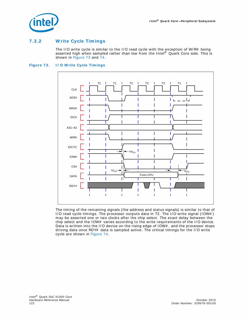
Intel® Quark Core—Peripheral Subsystem
7.3.2 Write Cycle Timings
The I/O write cycle is similar to the I/O read cycle with the exception of W/R# being asserted high when sampled rather than low from the Intel® Quark Core side. This is shown in Figure 73 and 74.
Figure 73. I/O Write Cycle Timings
The timing of the remaining signals (the address and status signals) is similar to that of I/O read cycle timings. The processor outputs data in T2. The I/O write signal (IOW#) may be asserted one or two clocks after the chip select. The exact delay between the chip select and the IOW# varies according to the write requirements of the I/O device. Data is written into the I/O device on the rising edge of IOW#, and the processor stops driving data once RDY# data is sampled active. The critical timings for the I/O write cycle are shown in Figure 74.
CLK
ADS#
M/IO#
D/C#
A31–A2
W/R#
IOCYC
IOW#
CS#
DATA
RDY#
From CPU
TWVD
T2 T2 T2 T2T1 T1
TDVD TDFD
Intel® Quark SoC X1000 CoreHardware Reference Manual October 2013122 Order Number: 329678-001US

Peripheral Subsystem—Intel® Quark Core
Figure 74. I/O Write Cycle Timing Analysis
Latches and data buffers can improve processor write performance. In Figure 75, I/O addresses and data are both latched in a configuration called a posted write. Posted writes help increase system performance by allowing the processor to complete a cycle without wait states. Once the data and address are latched, RDY# can be asserted during the first T2 of an I/O write cycle. Thus, the processor operation and the write cycle to the peripheral device can continue simultaneously. This is illustrated in Figure 76. The write cycle appears to be only two clocks long (from ADS# to RDY#) because the actual write overlaps other CPU bus cycles.
Figure 75. Posted Write Circuit
TWVD Write Signal Valid DelayTWVD = TPLDpd
= 10 ns
TDVD Write Data Valid DelayTDVD = TVD
† + TBUFpd= 19 + 9 = 28 ns
TDFD Write Data Float TimeTDFD = TFD
† – TBUFpd= 0 + 9 = 9 ns
†TVD = T10 = Intel® Quark Core processor write data valid delay (33 MHz) TFD = T11 = Intel® Quark Core processor write data float delay (33 MHz)
I/O
Device
I/ODataLatch
I/OAddressDecode
I/OAddress
Latch
DataBuffer
Address
Processor
Data I/O WriteData Bus
Intel® Quark SoC X1000 CoreOctober 2013 Hardware Reference ManualOrder Number: 329678-001US 123

Intel® Quark Core—Peripheral Subsystem
Figure 76. Timing of a Posted Write
CLK
T1 T1 T2T2
ADS
CPU
Latched
RDX#
Address
AddressCycle 1
Cycle 1 Cycle 2
Intel® Quark SoC X1000 CoreHardware Reference Manual October 2013124 Order Number: 329678-001US

Local APIC—Intel® Quark Core
8.0 Local APIC
8.1 Local APIC OverviewThe local APIC (LAPIC) receives interrupts from the processor’s interrupt pins, from internal sources, and SoC and sends these to the CPU for handling the interrupts. The LAPIC currently does not support sending/receiving inter processor interrupt (IPI) messages to and from other processors on the system bus. The local APIC consists of a set of APIC registers and associated hardware that control the delivery of interrupts to the processor core. The APIC registers are memory mapped and can be read and written using the MOV instruction.
Figure 77. LAPIC Diagram
Intel® Quark SoC X1000 CoreOctober 2013 Hardware Reference ManualOrder Number: 329678-001US 125

Intel® Quark Core—Local APIC
8.2 LAPIC Register StructureThe LAPIC registers are mapped into the 4KB APIC register space. All the registers are 32-bits, 64-bits, or 256-bits in width and are aligned on 128-bit boundaries. All the registers are accessed using load/store operations. The following table shows the LAPIC register address mapping and the different register fields.
Table 20. LAPIC Register Address Map and Fields (Sheet 1 of 5)
Address Register Name Software Read/Write Reset Value Description
FEE0_0000H Reserved
FEE0_0010H Reserved
FEE0_0020H LAPIC ID Register Read/Write[31:28] = Reserved[27:24] = 8’b0;[23:0] = Reserved
[27:24] = APIC_ID
FEE0_0030H LAPIC Version Register Read Only[7:0] = Version[23:16] = Max. LVT Entry
FEE0_0040H Reserved
FEE0_0050H Reserved
FEE0_0060H Reserved
FEE0_0070H Reserved
FEE0_0080H Task Priority Register (TPR) Read/Write [31:0] = 32’b0
[3:0] = Task Priority Sub Class[7:4] = Task Priority
FEE0_0090HReserved.Arbitration Priority Register (APR)
Not Supported.Read Only
Not Supported
FEE0_00A0H Processor Priority Register (PPR) Read Only [31:0] = 32’b0
[3:0] = Processor Priority Sub-Class[7:4] = Processor Priority
FEE0_00B0H EOI Register Write Only [31:0] = 32’b0 [7:0] = EOI vector
FEE0_00C0H Reserved
FEE0_00D0H Logical Destination Register (LDR) Read/Write [31:0] = 32’b0 [31:24] = Logical APIC_ID
FEE0_00E0H Destination Format Register (DFR)
Bits 0 -27 Read only, bits 28-31 Read/Write
[31:0] = All 1’s
[31:28] = Model1111 = Flat Model0000 = Cluster (Not Supported)
FEE0_00F0H Spurious Interrupt Vector Register
Bits 0-3,Read/Writes.Writes are dropped. Hard wired to All 1's.Bits 7-4 Read/Write; bits 9-31 Read only
[7:0] = h’FF[31:8] = All 0’s
[7:0] = Spurious Vector[7:4]= S/W can write[3:0] = 4'b1111 and writes are dropped.[8] = APIC S/W enable/disable[9] = Focus Processor Checking
FEE0_0100H throughFEE0_0170H
In-Service Register(ISR) Read only [255:0] = All 0’s
[255:16][15:0] = Reserved
FEE0_0180H throughFEE0_01F0H
Trigger Mode Register (TMR) Read only [255:0] = All 0’s
[255:16][15:0] = Reserved
FEE0_0200H throughFEE0_0270H
Interrupt Request Register (IRR) Read only [255:0] = All 0’s
[255:16][15:0] = Reserved
Intel® Quark SoC X1000 CoreHardware Reference Manual October 2013126 Order Number: 329678-001US
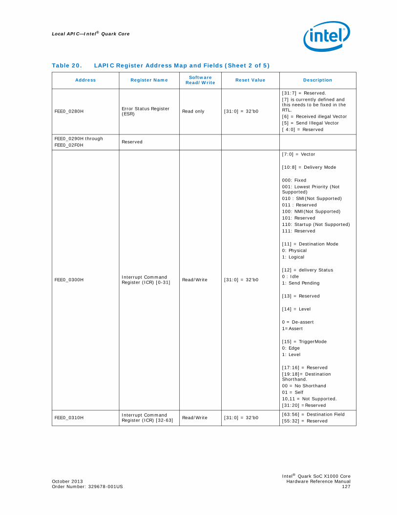
Local APIC—Intel® Quark Core
FEE0_0280H Error Status Register (ESR) Read only [31:0] = 32’b0
[31:7] = Reserved.[7] is currently defined and this needs to be fixed in the RTL.[6] = Received illegal Vector[5] = Send Illegal Vector[ 4:0] = Reserved
FEE0_0290H throughFEE0_02F0H
Reserved
FEE0_0300H Interrupt Command Register (ICR) [0-31] Read/Write [31:0] = 32’b0
[7:0] = Vector
[10:8] = Delivery Mode
000: Fixed001: Lowest Priority (Not Supported)010 : SMI(Not Supported)011 : Reserved100: NMI(Not Supported)101: Reserved110: Startup (Not Supported)111: Reserved
[11] = Destination Mode0: Physical1: Logical
[12] = delivery Status0 : Idle1: Send Pending
[13] = Reserved
[14] = Level
0 = De-assert1=Assert
[15] = TriggerMode0: Edge1: Level
[17:16] = Reserved[19:18]= Destination Shorthand.00 = No Shorthand01 = Self10,11 = Not Supported.[31:20] =Reserved
FEE0_0310H Interrupt Command Register (ICR) [32-63] Read/Write [31:0] = 32’b0
[63:56] = Destination Field[55:32] = Reserved
Table 20. LAPIC Register Address Map and Fields (Sheet 2 of 5)
Address Register Name Software Read/Write Reset Value Description
Intel® Quark SoC X1000 CoreOctober 2013 Hardware Reference ManualOrder Number: 329678-001US 127

Intel® Quark Core—Local APIC
FEE0_0320H LVT Timer Register Read/Write [31:0] = 0001_0000H
[7:0] = Vector[11:8] = Reserved[12] = Delivery Status0: Idle1: Send Pending[15:12] = Reserved[16] = Mask0: Not Masked1: Masked[17] = Timer Mode0: One-Shot1: Periodic[31:18] = Reserved
FEE0_0330H Reserved Read/Write
FEE0_0340H Reserved Read/Write
FEE0_0350H LVT LINT0 Register Read/Write [31:0] = 0001_0000H
[7:0] = Vector[10:8] = Delivery Mode000: Fixed010: SMI(Not Supported)100: NMI(Not Supported)111: ExtINT(Not Supported)101: ReservedAll other combinations are Reserved
[11] = Reserved[12] = Delivery Status0: Idle1: SendPending[13] = Interrupt Input Pin polarity0: Active High1: Active Low[14] = Remote IRR Flag (Read Only)1: LAPIC accepts the interrupt for servicing0: EOI command is received from the CPU.[15] = Trigger Mode0: Edge1: Level[16] = Mask0: Enables Reception of the Interrupt1: Inhibits Reception of the Interrupt[31:17] = Reserved
Table 20. LAPIC Register Address Map and Fields (Sheet 3 of 5)
Address Register Name Software Read/Write Reset Value Description
Intel® Quark SoC X1000 CoreHardware Reference Manual October 2013128 Order Number: 329678-001US

Local APIC—Intel® Quark Core
FEE0_0360H LVT LINT1 Register Read/Write [31:0] = 0001_0000H
[7:0] = Vector[10:8] = Delivery Mode000: Fixed010: SMI(Not Supported)100: NMI(Not Supported)111: ExtINT(Not Supported)101: ReservedAll other combinations are Reserved
[11] = Reserved[12] = Delivery Status0: Idle1: SendPending[13] = Interrupt Input Pin polarity0: Active High1: Active Low[14] = Remote IRR Flag (Read Only)1: LAPIC accepts the interrupt for servicing0: EOI command is received from the CPU.[15] = Trigger Mode0: Edge1: Level[16] = Mask0: Enables Reception of the Interrupt1: Inhibits Reception of the Interrupt[31:17] = Reserved
FEE0_0370H LVT Error Register Read/Write [31:0] = 0001_0000H
[7:0] = Vector[11:8] = Reserved[12] = Delivery Status0: Idle1: Send Pending[15:13] = Reserved[16] = Mask[31:17] = Reserved
FEE0_0380H Initial Count Register (for Timer) Read/Write [31:0] = 32’b0 [31:0] = Initial CountValue
FEE0_0390H Current Count Register (for Timer) Read Only [31:0] = 32’b0 [31:0] = Current Count Value
Table 20. LAPIC Register Address Map and Fields (Sheet 4 of 5)
Address Register Name Software Read/Write Reset Value Description
Intel® Quark SoC X1000 CoreOctober 2013 Hardware Reference ManualOrder Number: 329678-001US 129

Intel® Quark Core—Local APIC
The LAPIC can be enabled/disabled using the APIC software enable/disable flag in the spurious-interrupt vector register. Each entry in the LVT has a mask bit that can be used to inhibit interrupts from being delivered to the processor from selected local interrupt sources like the APIC Timer, etc.
The IA32_APIC_BASE MSR is not supported on Intel® Quark SoC X1000 Core and so the address of the LAPIC registers cannot be relocated. During Reset the APIC_ID is hard coded to All 0's. The BE0# - BE3# are not sampled to get the APIC_ID during Reset. The LAPIC supports the APIC timer, and internal APIC error detector. The LAPIC handles interrupts through local vector table (LVT), the error status register (ESR), the divide configuration register and the initial count and current count registers.
The LVT enables the software to program the registers to specify the manner in which the local interrupts are delivered to the Intel® Quark SoC X1000 Core. The LVT error register specifies the interrupt delivery when the APIC detects an internal error. The LAPIC has an error status register (ESR) that it uses to record errors that it detects on the vectors when handling interrupts. The IA-32 valid interrupt vectors are 256 vector numbers, ranging from 0 through 255. The LAPIC supports 240 of these vectors (16 - 255) as valid vectors. When an interrupt vector in the range of 0 to 15 is sent or received through the LAPIC, the LAPIC indicates an illegal vector in its Error Status Register. The IA-32 reserves vectors 16 through 31 for predefined interrupts, and exceptions. The LAPIC doesnot treat them as illegal vectors. An APIC error interrupt is generated when the local APIC sets one of the error bits in the ESR. When an APIC error is detected the LVT error register allows selection of interrupt vector to be delivered to the CPU.
8.2.1 APIC Timer
The LAPIC contains a 32-bit programmable timer that is available to software to time events or operations. This timer is set up by programming four registers: the divide configuration registers, the initial count and current count register, and the LVT timer register. The time base for the timer is derived from the processor's bus clock, divided by the value specified in the divide configuration register. The timer can be configured through the timer LVT entry for one-shot or periodic operation. In one-shot, the time is started by programming its initial count register. The initial count is value is then copied
FEE0_03A0H through FEE0_03D0H Reserved
FEE0_03E0H Divide Config. Register (for Timer) Read/Write [31:0] = 32’b0
[3:0] = Divide Value; [2] hard coded to 1’b0.{[3],[1:0]}
000: Divide by 2001: Divide by 4010: Divide by 8011:Divide by 16100: Divide by 32101: Divide by 64110: Divide by 128111: Divide by 1
FEE0_03F0H Reserved
Table 20. LAPIC Register Address Map and Fields (Sheet 5 of 5)
Address Register Name Software Read/Write Reset Value Description
Intel® Quark SoC X1000 CoreHardware Reference Manual October 2013130 Order Number: 329678-001US
Local APIC—Intel® Quark Core
into the current count register (ccr) and count-down begins. After the timer reaches zero, an timer interrupt is generated and the timer remains at its value until reprogrammed.
In periodic timer, the current count register is automatically reloaded from the initial count register when the count reaches 0 and a timer interrupt is generated and the count-down is repeated. If during the count-down process the initial count register is set, counting willrestart, usingthe new initial-count value. The LVT timer register determines the vector number that is delivered to the processor with the timer interrupt that is generated when the timer count reaches zero. The mask flag in the LVT timer register can be used to mask the timer interrupt.
8.2.2 Interrupt Control Register (ICR), Logical Destination Register (LDR), Destination Format Register (DFR)
The ICR is a 64-bit register in the LAPIC that allows the software running on the CPU to specify and direct the processor to interrupt itself. The inter processor interrupts (IPI) are not currently supported. When the Destination Short hand field of the ICR is programmed to Self (2'b01) it allows the software to interrupt the CPU on which it is executing and delivers the interrupt internally. The Logical Destination Register (LDR) and Destination Format Register (DFR) are used in conjunction with the logical destination mode and message destination address (MDA) field in the ICR to select the destination CPU. The destination mode field in the ICR selects either physical (0) or logical (1) destination mode. If the destination mode is set to physical then bits [59:56] of ICR contain the APICID of the target processor. If the destination mode is set to logical, the interpretation of the 8-bit destination field in the ICR depends on the settings of the DFR and LDR registers. Upon receiving the IPI message that was sent using logical destination mode, the LAPIC compares the MDA in the message with the values in the LDR and DFR to determine if it should accept and handle the IPI.
8.2.3 Interrupt and Task Priority
The interrupts delivered to the processor through LAPIC has an implied priority based on its vector number. The LAPIC uses this priority to determine when to service the interrupt relative to the other activities of the processor. The interrupt priority (for vectors 16 to 255) is determined using vector/16. The quotient is rounded to the nearest integer with 1 being the lowest priority and 15 is the highest. Vectors 0 to31 are reserved. The priorities of user defined interrupts range from 2 to 15.
The task priority allows the software to set a priority threshold for interrupting the processor. The processor will service only those interrupts that have a priority higher than that specified in the task priority register (TPR). If software sets the task priority in the TPR to 0, the processor will handle all the interrupts, it is set to 15, all interrupts are inhibited from being handled, (except NMI, SMI, and ExtINT which are currently not supported). This mechanism allows the operating system to temporarily block specific interrupts (low priority interrupts) from disturbing high-priority work that the processor is currently working. The TPR value that the software can write is between 0 to 15.
The processor priority is set by the processor ( value 0 to 15) and is written into the processor priority register (PPR). The processor priority represents the current priority at which the processor is executing. It is used to determine whether a pending interrupt can be sent to the processor. The Processor priority is set to either to the highest priority interrupt in the ISR or to the current task priority, whichever is higher.
8.2.4 Fixed Interrupts
The LAPIC queues the fixed interrupts that it accepts either in the interrupt request register (IRR) or in-service register (ISR). These are 256-bit registers and each bit represents an interrupt vector number. Vector 0 - 15 are reserved.
Intel® Quark SoC X1000 CoreOctober 2013 Hardware Reference ManualOrder Number: 329678-001US 131

Intel® Quark Core—Local APIC
The IRR contains the active interrupt request that has been accepted but not yet dispatched to the processor for servicing. When the LAPIC accepts an interrupt, it sets the bit in the IRR that corresponds to the vector of the accepted interrupt. When the CPU is ready to handle the next interrupt, the LAPIC clears the highest priority IRR bit that is set and sets the corresponding ISR bit. The Vector for the highest priority bit is set in the ISR is then dispatched to the processor core for servicing.
When the CPU is servicing the highest priority interrupt, the LAPIC can send additional fixed interrupts by setting bits in the IRR. When the interrupt service routine issues a write to the EOI register the LAPIC clears the highest priority ISR bit that is set.
If more than one interrupt is generated with the same vector number, the LAPIC can set the bit for the vector both in the IRR and the ISR. The IRR and ISR registers can queue no more than two interrupts per priority level, and will reject other interrupts that are received within the same priority level.
If the LAPIC receives an interrupt with a priority higher than that of the interrupt currently in serviced, and interrupts are enabled in the processor core, the LAPIC dispatches the higher priority interrupt to the processor immediately without waiting for a write to the EOI register. The currently executing interrupt handler is then interrupted so the higher priority interrupt can be handled. When the handling of the higher priority interrupt has been completed, the servicing of the interrupted interrupt is resumed.
The trigger mode register (TMR) indicates the trigger mode of the interrupt. When the interrupt is accepted into the IRR, the corresponding TMR bit is cleared for edge-triggered interrupts and set for level-triggered interrupts. If a TMR bit is set when an EOI cycle for its corresponding interrupt vector is generated, and EOI message is sent to all I/O APIC's.
8.2.5 End of Interrupt (EOI)
For all interrupts (except those delivered with the NMI, SMI, ExtINT which are currently not supported) the interrupt handler must include a write to the end-of-interrupt (EOI) register. This write must occur at the end of the handler routine, sometimes before the IRET instruction. This action indicates that the servicing of the current interrupt is complete and LAPIC can issue next interrupt from the ISR.
Intel® Quark SoC X1000 CoreHardware Reference Manual October 2013132 Order Number: 329678-001US

Clocking Considerations and System Debugging—Intel® Quark Core
9.0 Clocking Considerations and System Debugging
9.1 Clocking ConsiderationsThe Intel® Quark Core is based on a legacy dual phase latch based design, in which each cycle was divided into two phases. A non-overlapping clocking scheme was needed in the dual phase design in order to meet min delay requirements. This scheme was good for unevenly partitioned logic. To ease synthesis, the Intel® Quark Core SIP design has been converted to a flop based design.
9.1.1 Intel® Quark Core Clocking Architectures
The Intel® Quark Core design supports three different clocking architectures:• Two Phase• Single Phase• 1-clock
The next sections provide a summary of each of these clocking implementations
Note: With the performance, area and power benefits inherent with the 1-clock design, Intel® Quark SoC X1000 customers are urged to use the 1-clock configuration.
9.1.1.1 Two Phase Flop Design
Figure 78 depicts the two phase latch to two phase flop design transformation. In this transformation, the 5 cycle CPU pipeline is maintained as 5 cycles of the xclk input.
The two phase design would have timing paths from the rising edge of xclk to the rising edge of xclknn essentially creating phase paths.
Figure 78. Two phase flop based Intel® Quark Core design
Data
xclk
CB
LOGIC LA1 LA2
xclknn = NOT (xclk)
FF1CB
LOGICFF2
TWO PHASE LATCH BASED
DESIGN
TWO PHASE FLOP BASED
DESIGN
xclk xclknn = NOT (xclk)
Intel® Quark SoC X1000 CoreOctober 2013 Hardware Reference ManualOrder Number: 329678-001US 133

Intel® Quark Core—Clocking Considerations and System Debugging
9.1.1.2 LMT Single Phase Flop Design
Figure 80 depicts the two phase latch to single phase flop design transformation. This transformation increases the CPU pipeline depth to 10 xclk cycles. Therefore, to get the same performance as a Dual Phase clock design, a Single Phase design will have to run at 2X the frequency.
The single phase clock design has timing paths from the rising edge of xclk to the rising edge of xclknn, but in this case xclk = xclknn as shown below. This results in full cycle timing paths. The advantage of the single phase design is that it is less sensitive to duty cycle of the input clocks and capable of reaching higher frequencies than the two phase flop design.
Figure 79. Clock waveforms for a two phase clock design
Tp
xclk
xclknn
Tp/2
Timing path
Figure 80. Single phase flop based Intel® Quark Core design
Data
xclk
CB
LOGIC LA1 LA2
xclknn = NOT (xclk)
FF1CB
LOGICFF2
TWO PHASE LATCH BASED
DESIGN
SINGLE PHASE FLOP BASED
DESIGN
xclk xclknn = xclk
Figure 81. Clock Waveforms for Single Phase flop based Intel® Quark Core design
Tp
xclk
xclknn
Timing path
Intel® Quark SoC X1000 CoreHardware Reference Manual October 2013134 Order Number: 329678-001US
Clocking Considerations and System Debugging—Intel® Quark Core
The down-side of the single phase flop design is power. Since the clock frequency needs to double for constant performance, the clock related power is significantly greater for the single phase design compared to the two phase flop design.
9.1.1.3 Intel® Quark Core 1-clock Flop Design
With the Intel® Quark Core 1.0 release, a new clocking option is available. Conceptually, the 2 phase latch design is ported to an optimized 1-clock flop based design. The 5 cycle CPU pipeline is maintained. Timing paths are all full cycle paths.
In the 1-clock design, pipe stages are optimized and redundant flops are removed. Also, unlike the two phase and single phase designs, a only a single clock tree is routed. Thus, the 1-clock design has the following advantages over the two-phase and single-phase designs:
• Reduced flop count results in smaller area, lower active and leakage power.• A single routed clock tree results in smaller area, lower active and leakage power
and improved timing due to closer point of divergence (POD) - i.e. less clock uncertainty.
Note: With the performance, area and power benefits inherent with the 1-clock design, Intel® Quark SoC X1000 customers are urged to use the 1-clock configuration.
9.1.2 SoC / Intel® Quark Core Clock Architecture
A typical SoC could have a SoC PLL which locks to a reference clock from a reference source. This PLL is followed by a divider and generates the requisite clocks for the Intel® Quark Core. Given below are block diagrams of the typical SOC/LMT clock architectures for the three Intel® Quark Core clocking options.
Figure 82. Intel® Quark Core 1-Clock Flop Based Design
D ata
xclk
C B
LO GIC LA1 LA2
xclknn = NOT (xclk)
FF1C B
LO GICFFX
TW O PHASE LATCH BASED
DESIGN
1-Clock FLOP BASED
DESIGN
xclk xclk
Figure 83. Intel® Quark Core Clocking Architecture Block Diagram for two-phase clock
x clkRef clk
SOC PLLMIA Divider
fvco_s oc
xclknn
POD
TWO-PHASE CLOCK
xclknn = not(xclk)
LMTCPU
Intel® Quark SoC X1000 CoreOctober 2013 Hardware Reference ManualOrder Number: 329678-001US 135

Intel® Quark Core—Clocking Considerations and System Debugging
Note in the two-phase clocking option, the SoC supplies Intel® Quark Core with two input clocks - xclk, xclknn. These clocks are 180 degrees out of phase. Internally, Intel® Quark Core implements two separate trees. For clock uncertainty, the point of divergence (POD) is outside of Intel® Quark Core in the SoC, where the clocks bifurcate. This implies that all the xclk<->xclknn paths will receive worst-case clock uncertainty based in this POD.
In the single-phase clock design, the SoC still supplies the Intel® Quark Core with two clocks - xclk and xclknn. However, these clocks are in-phase. The POD is still outside of Intel® Quark Core in the soC. This implies that all the xclk<->xclknn paths will receive worst-case clock uncertainty based in this POD.
With the 1-clock design, the SoC provides Intel® Quark Core with one clock - xclk. All sequential elements within Intel® Quark Core use this single clock. The clock POD is within the LMT design, which allows for lower clock uncertainty.
9.1.3 Intel® Quark Core Core/Bus/SoC Clock Ratio
The Intel® Quark Core is divides into two clock zones the core clock frequency and the bus clock frequency, which gives the ability to throttle the core or bus.
Figure 84. Intel® Quark Core Clocking Architecture Block Diagram for single-phase clock
xclkRef clk
SOC PLLL MT D ivider
fvco_soc
xclkn n
PO DSINGLE-PHASE CLOCK
LMTCPU
Figure 85. Intel® Quark Core Clocking Architecture Block Diagram for 1-clock design
xclkRef clk
SOC PLLMIA Divider
fvco_s oc
PO D
1-Clock LMT Design
LMTCPU
Intel® Quark SoC X1000 CoreHardware Reference Manual October 2013136 Order Number: 329678-001US

Clocking Considerations and System Debugging—Intel® Quark Core
As shown in Table 22, currently only a 1:1 core to bus clock ratio is supported. Additional ratios may be supported in future releases of Intel® Quark Core.
9.1.4 Clock Skew and Uncertainty
• Clock skew = Max Insertion Delay - Min Insertion Delay — Systematic Variation a functions of distance and no of sinks— Prime Time sets the skew to zero and calculates real skew value case by case
by traversing the clock tree.• Clock uncertainty - Systematic or Random
— Systematic components add linearly together— Random components root sum square— Related to the POD (point of divergence) and depth of buffers or Insertion
delay.• Cross clock vs. Same Clock Skew
— Since most of the paths in this design will go from xclk to xclknn, the cross clock skew is going to be really important.
9.1.4.1 Clock Uncertainty Components and Numbers
Table 22 lists the uncertainty components and totals. These numbers are applicable to both P1271 and P1269 and have been used for our analysis. Note these numbers are meant as a guideline, the SoC groups depending on their clock tree implementation will refine these numbers.
Figure 86. Intel® Quark Core Clock Zones
Table 21. Intel® Quark Core Supported Clock Ratios
Intel® Quark Core SoC
core bus fabric
Fcore Fbus FSoC
1 1 1
2 1 1
3 1 1
4 1 1
Intel® Quark SoC X1000 CoreOctober 2013 Hardware Reference ManualOrder Number: 329678-001US 137

Intel® Quark Core—Clocking Considerations and System Debugging
9.2 Building and Debugging a Intel® Quark Core-Based System Although a Intel® Quark Core-based system designer should plan the entire system, it is necessary to begin building different elements of the core and begin testing them before building the final system. If a printed circuit board layout has to be done, the whole system may be simulated before generating the net list for the layout vendor. It is advisable to work with a preliminary layout to avoid the problems associated with wire wrap boards that operate at high frequencies.
Figure 87 shows how the Intel® Quark Core is implemented in the Intel® Quark SoC X1000.
Table 22. Intel® Quark Core Clock Uncertainty Numbers
Clock Uncertainty Components Two Phase (ps)
Single Phase (ps)
Single Clock (ps)
Formulat ion Comments
SOC Clock Tree MAX Insertion Delay(ns) 200 0 0Assumed Insertion Delay Since we are shorting for single phase. The POD of the Single phase will be righ at the boundary of the MIA CORE.
SOC Clock Tree Insertion Delay Supply Variance (ps) 12 0 0 6% Using the curve fit equationSOC Clock Tree Insertion Delay Mismatch(ODV) (ps) 12 0 0 6%SOC Clock Tree Insertion Delay Aging (ps) 7 0 0 3.5%
LMT Core Clock Tree Max Insertion Delay(ns) 400 400 500For Single clock the POD would be closer to the luanch/Capture Flops
LMT Clock Tree Insertion Delay Supply Variance (ps) 24 24 12 6%
LMT Clock Tree Insertion Delay Mismatch(ODV) (ps) 24 24 12 6%
The total ODV saturates at about 45ps, when the total number of buffers in the insert ion delay chain increases from 24. Additionally since the ODV for the global clock tree would be common it should not be added into the unc f or the same clock. On top of that the point of divergence for the for two timed flops may not be root of the local tree.
LMT Clock Tree Insertion Delay Aging (ps) 14 14 7 3.5%
Duty Cycle Variability 40 0 0 5% 2% duty cycle variation for 500MHzSOC PLL Cycle- to-Cycle Jitter 60 60 60Addit ional Slop 35.54 21.59 16.79Total clock Uncertainity 177.68 107.94 83.97 Using RSS for adding the random componentsTotal clock Uncertainity w/GB 213.21 129.53 100.76
Intel® Quark SoC X1000 CoreHardware Reference Manual October 2013138 Order Number: 329678-001US
Clocking Considerations and System Debugging—Intel® Quark Core
The following steps are usually carried out in designing with the Intel® Quark Core. 1. Clock circuitry should consist of an oscillator and fast buffer. The CLK signal should
be clean, without any overshoot or undershoot.2. The reset circuitry should be designed as shown in Chapter 4.0, “Bus Operation”.
This circuitry is used to generate the RESET # signal for the Intel® Quark Core. The system should be checked during reset for all of the timings. The clock continues to run during these tests.
3. The INT and HOLD pins should be held low (deasserted). The READY# pin is held high to add additional delays (wait states) to the first cycle. At this instance, the Intel® Quark Core is reset, and the signals emitted from it are checked for the validity of the state. The Intel® Quark Core starts executing instructions at location FFFFFFF0H after reset. The address latch is connected and the address is verified.
4. The PAL implementing the address decoder should be connected to the Intel® Quark Core.
Figure 87. Intel® Quark SoC X1000 Core used in Intel® Quark SoC X1000
Intel® Quark SoC X1000 CoreOctober 2013 Hardware Reference ManualOrder Number: 329678-001US 139

Intel® Quark Core—Clocking Considerations and System Debugging
9.2.1 Debugging Features of the Intel® Quark Core
The Intel® Quark Core provides several features which simplify the debugging process for the system hardware designer. The device offers the following on-chip debugging aids:
• Breakpoint Instruction: describes code execution breakpoint opcode. • Single-Step Trap: describes single-step capability provided by the TF bit in the flag
register. • Debug Registers and Debug Control Register (DR7): describes code and data
breakpoint capability as provided by the debug registers (DR3–DR0, DR6 and DR7).
• Debugging Overview: describes ITP and JTAG Debugging
9.2.2 Breakpoint Instruction
The Intel® Quark Core provides a breakpoint instruction that can be used by software debuggers. This instruction is a single byte opcode and generates an exception 3 trap when it is executed. In a typical environment a debugger program can place the breakpoint instruction at various points in the program. The single-byte breakpoint opcode is an alias for the two-byte general software interrupt instruction, INTn where n=3. The only difference between INT 3 and INT n is that INT3 is never IOPL-sensitive but INTn is IOPL-sensitive in Protected Mode and Virtual 8086 Mode.
9.2.3 Single-Step Trap
The Intel® Quark Core supports the legacy single-step feature. If the single stepflag bit (bit 8, TF) is set to 1 in the EFLAG register, a single step exception occurs. This exception is auto-vectored to exception 1 and occurs immediately after completion of the next instruction. Typically a debugger sets the TF bit of the EFLAG register on the debugger's stack followed by transfer of the control to the user program. The debugger also loads the flag image (EFLAG) via the IRET instruction. The single-step trap occurs after execution of one instruction of the user program.
Since the exception 1 occurs right after the execution of the instruction as a trap, the CS:EIP pushed onto the debugger's stack points to the next unexecuted instruction of the program which is being debugged, merely by ending with an IRET instruction.
After MOV to SS and POP to SS instructions, the Intel® Quark Core masks some exceptions, including single-step trap exceptions.
9.2.4 Debug Registers
The Intel® Quark Core has an advanced debugging feature. It has six debug registers that allow data access breakpoints as well code access breakpoints. Since the breakpoints are indicated by on-chip registers, an instruction execution breakpoint can be placed in ROM code or in code shared by several tasks. Neither of these is supported by the INT3 breakpoint opcode.
The debug register provides the ability to specify four distinct breakpoint addresses, control options, and read breakpoint status. When the CPU goes through reset, the breakpoints are all in the disabled state. Hence the breakpoints cannot occur unless the debug resisters are programmed.
It is possible to specify up to four breakpoint addresses by writing into debug registers. The debug registers are shown in Figure 88. The addresses specified are 32-bit linear addresses. The processor hardware continuously compares the linear breakpoint addresses in DR3–DR0 with the linear addresses generated by executing software.
Intel® Quark SoC X1000 CoreHardware Reference Manual October 2013140 Order Number: 329678-001US

Clocking Considerations and System Debugging—Intel® Quark Core
When the paging is disabled then the linear address is equal to the physical address. If the paging is enabled then the linear address is translated to a 32-bit address by the on-chip paging unit. Whether paging is enabled or disabled, the breakpoint register holds linear addresses.
Figure 88. Debug Registers
31 16 15 0
Breakpoint 0 Linear Address DR0
Breakpoint 1 Linear Address DR1
Breakpoint 2 Linear Address DR2
Breakpoint 3 Linear Address DR3
Intel Reserved. Do not define. DR4
Intel Reserved. Do not define. DR5
0 BT
BS
BD 0 0 0 0 0 0 0 0 0 B
3B2
B1
B0 DR6
LEN3
R3
W3
LEN2
R2
W2
LEN1
R1
W1
LEN0
R0
W0 0 0 G
D 0 0 0 GE
LE
G3
L3
G2
L2
G1
L1
G0
L0 DR7
31 16 15 0
Note: 0 indicates Intel reserved: Do not define.
LENiEncoding
BreakpointField Width
Usage of Least Significant Bits in Breakpoint Address
Register i, (i = 0–3)
00 1 Byte All 32 bits used to specify a single-byte breakpoint field.
01 2 Byte
A31–A1 used to specify a two-byte word-aligned breakpoint field. A0 in breakpoint address register is not used.
10
Undefined–Do not use
this encoding.
11 4 Byte
A31–A2 used to specify a four-byte dword-aligned breakpoint field. A0 and A1 in breakpoint address register are not used.
DR2 = 00000005H; LEN2 = 00B
DR2 = 00000005H; LEN2 = 01B
DR2 = 00000005H; LEN2 = 11B
31 0
00000008H
BKPT FLD2 00000004H
00000000H
31 0
00000008H
00000004H
00000000H
31 0
00000008H
00000004H
00000000H
BKPT FLD2
BKPT FLD2
Intel® Quark SoC X1000 CoreOctober 2013 Hardware Reference ManualOrder Number: 329678-001US 141

Intel® Quark Core—Clocking Considerations and System Debugging
9.2.5 Debug Control Register (DR7)
A debug control register, DR7 shown in Figure 88, allows several debug control functions such as enabling the breakpoints and setting up several control options for the breakpoints. There are several fields within the debug control register. These are discussed below:
LENi (breakpoint length specification bits). A 2-bit LEN field exists for each of the four breakpoints. It specifies the length of the associated breakpoint field. It is possible to have three different choices: 1 byte, 2 bytes and 4 bytes. LENi field encoding is shown in Table 23.
The LENi field controls the size of the breakpoint field i by controlling whether all the low order linear address bits in the breakpoint address register are used to detect the breakpoint event. Therefore, all breakpoint fields are aligned: 2-byte breakpoint fields begin on word boundaries, and 4-byte breakpoint fields begin on dword boundaries.
A 2-bit RW field exists for each of the four breakpoints. The 2-bit field specifies the type of usage which must occur in order to activate the associated breakpoint.
RW encoding 00 is used to setup an instruction execution breakpoint. RW encodings 01 or 11 are used to setup write only or read-only or read/write data breakpoints. The data breakpoint can be setup by writing the linear address into DRi. For data breakpoints, RWi can:
= 01 M write only= 11 M read/writeLENi = 00, 01, 11.
An instruction execution breakpoint can be setup by writing the address of the beginning of the instruction into DRi. RWi must equal 00 and LENi must equal 00 for instruction execution breakpoints. If the instruction beginning at the breakpoint address is about to be executed, the instruction execution breakpoint has occurred, and the breakpoint is enabled, an exception 1 fault occurs before the instruction is executed.
GD (Global Debug Register access detect). The debug registers can only be accessed in real mode or at privilege level 0 in Protected Mode. The GD bit when set provides extra protection against any debug register access even in Real Mode or at privilege level 0 in Protected Mode. This additional protection feature is provided to guarantee that a software debugger can have full control over the debug register resources when required.
The Intel® Quark Core always does exact data breakpoint matching regardless of the GE/LE bit settings. Any data breakpoint trap is reported after completion of the instruction that caused the operand transfer. Reporting is provided by forcing the Intel® Quark Core execution unit to wait for the completion of data operand transfers before beginning execution of the next instruction.
Table 23. LENi Fields
RW Encoding Usage Causing Breakpoint
00 Instruction execution only
01 Data writes only
10 Undefined—Do not use this encoding
11 Data reads and writes only
Intel® Quark SoC X1000 CoreHardware Reference Manual October 2013142 Order Number: 329678-001US

Clocking Considerations and System Debugging—Intel® Quark Core
When the Intel® Quark Core switches to a new task, the LE bit is cleared. Thus, LE enables fast switching from one task to another task. To avoid having exact data breakpoint match enabled in the new task, the LE bit is cleared by the processor during the task switch. Note that exact data breakpoint match must be re-enabled under software control.
The GE bit supports exact data breakpoint match that is to remain enabled during all tasks executing in the system. The Intel® Quark Core GE bit is unaffected during a task switch.
Note: Instruction execution breakpoints are always reported.
G, L (breakpoint enable, global and local). Associated breakpoints are enabled when either G or L are set. When this happens the Intel® Quark Core detects the ith breakpoint condition, then the exception 1 handler is invoked.
Debug status register. A debug status register, DR6 allows the exception 1 handler to easily determine why it was invoked. Exception 1 handler can be invoked as a result of one of the several events as documented in the datasheet. This register contains single-bit flags for each of the possible events invoking exception 1. Some of these events are faults while others are traps.
9.2.6 Debugging Overview
Once the Intel® Quark Core-based system is designed and the printed circuit board is fabricated and stuffed, the next step is to debug the hardware in increments.
The design of a microprocessor-based system can be subdivided into several phases. The design starts with preparation of the system specification followed by conceptual representation in the form of block diagram. The next phase is implementing the design, which consists of the hardware design and the software design occurring in parallel. Hardware debugging usually begins by testing the system with short test programs. Initially the power and ground lines are tested for opens and shorts followed by the testing of the reset function. After the hardware passes these programs, the hardware/software integration phase begins. The test programs are then replaced by the application software and complete system is debugged.
When there are both hardware and software problems, it can be difficult to isolate each. Several types of testing systems are available to assist in this process. The most common type is the in-circuit emulator, which plugs into the microprocessor socket and allows the operation of the system to be controlled and monitored. In-circuit emulators usually include memory that can be used in place of the prototype memory. Another useful test tool is the logic analyzer, which captures the “trace” of the bus activity and displays the sequence of bus cycles that were executed. Most in-circuit emulators also provide this function, which is invaluable for both hardware and software debugging. Test programs can be run from an ICE or a monitor.
The Intel® Quark Core contains a JTAG (Joint Test Action Group) test-logic unit, which you can use to test the processor and its connections to the system. The JTAG specifications with which this unit complies are documented in Standard 1149.1-1990, IEEE Standard Test Access Port and Boundary Scan Architecture and its supplement, Standard 11.49.1a-1993.
Refer to the “Debug Port and JTAG/TAP” chapter in the Intel® Quark SoC X1000 EDS for more details.
§ §
Intel® Quark SoC X1000 CoreOctober 2013 Hardware Reference ManualOrder Number: 329678-001US 143