Embed Size (px)
Citation preview

Calhoun: The NPS Institutional Archive
Theses and Dissertations Thesis Collection
1995-06
Harmonic distortion correction using active power
line conditioners
Jones, Kevin David.
Monterey, California. Naval Postgraduate School
http://hdl.handle.net/10945/31450

NAVAL POSTGRADUATE SCHOOL MONTEREY, CALIFORNIA
THESIS
HARMONIC DISTORTION CORRECTION USING ACTIVE POWER LINE CONDITIONERS
by
Kevin David Jones
June 1995
Thesis Advisor: Robert W. Ashton
Approved for public release; distribution is unlimited
19951109 075 DTIC QUAIOT INSPECTED 8

REPORT DOCUMENTATION PAGE Form Approved OMB No. 0704-0188
1. AGENCY USE ONLY (Leave blank) 2. REPORT DATE
June 1995
3. REPORT TYPE AND DATES COVERED
Engineer's and Master's Thesis
4. TITLE AND SUBTITLE HARMONIC DISTORTION CORRECTION USING ACTIVE POWER LINE CONDITIONERS
6. AUTHOR(S)) Kevin D. Jones
7. PERFORMING ORGANIZATION NAME(S) AND ADDRESS(ES)
Naval Postgraduate School Monterey, Ca 93943-5000
9. SPONSORING/MONITORING AGENCY NAME(S) AND ADDRESS(ES)
5. FUNDING NUMBERS
8. PERFORMING ORGANIZATION REPORT NUMBER
10. SPONSORING/MONITORING AGENCY REPORT NUMBER
11. SUPPLEMENTARY NOTES . The views expressed in this thesis are those of the author and do not reflect the official policy or position of the Department of Defense or the U.S. Government
12a. DISTRIBUnON/AVAILABIUTY STATEMENT
Approved for public release; distribution is unlimited.
12b. DISTRIBUTION CODE
13. ABSTRACT (Maximum 200 words)
Harmonic distortion of a voltage wave form on a local distribution system may have many effects, such as: protective device malfunctions, medical equipment failures, and increased noise generation and bearing wear of rotating equipment In the past these effects have been tolerated. Advances in semiconductor technology in the past two decades have produced devices that can handle large amounts of power efficiently and safely. These advances have led to an increased number of loads mat contribute to the bus voltage distortion.
These same advances that have made the distortion problem worse also have given rise to devices that can be used to actively correct the problem Active Power Line Conditioners (APLCs) use voltage or current converters to improve harmonic distortion on local buses. APLCs use information from current or power sensors that are spread throughout the distribution system in order to correct the voltage wave form distortion. These sensors are difficult and costly to install. This Ihesis presents an APLC that produces its distortion canceling signal using only bus voltage information thus reducing the distribution sample points to one. The LabVIEW graphical progimuning language is used for «rninling and control of the APLC
14. SUBJECT TERMS Active Power Line Conditioner, Harmonic Distortion
17. SECURITY CLASSIFICATION OF REPORT unclassified
18. SECURITY CLASSIFICATION OF THIS PAGE .. . .- ,
Unclassified
15. NUMBER OF PAGES 61
16 PRICE CODE
19. SECURITY CLASSIFICATION OF ABSTRACT rr ...
Unclassified
20. LIMITATION OF ABSTRACT UL
»dT^n


Approved for public release; distribution is unlimited
HARMONIC DISTORTION CORRECTION USING ACTIVE POWER LINE CONDITIONERS
Kevin David Jones Lieutenant, United States Navy
B.S., Oregon State University, 1988
Submitted in partial fulfillment of the requirements for the degree of
ELECTRICAL ENGINEER
and
MASTER OF SCIENCE IN ELECTRICAL ENGINEERING
from the
NAVAL POSTGRADUATE SCHOOL
Author:
Approved by:
June 1995
Kevin David Jones
Robert W. Ashton, Thesis Advisor
Michael K. Shields, Second Reader
Michael A. Morgan, CJ^drman Department of Electrical and Computer Engineering
ill

IV

ABSTRACT
Harmonic distortion of a voltage waveform on a local distribution system may
have many effects, such as: protective device malfunctions, medical equipment failures,
and increased noise generation and bearing wear of rotating equipment. In the past these
effects have been tolerated. Advances in semiconductor technology in the past two
decades have produced devices that can handle large amounts of power efficiently and
safely. These advances have led to an increased number of loads that contribute to the bus
voltage distortion.
These same advances that have made the distortion problem worse also have given
rise to devices that can be used to actively correct the problem. Active Power Line
Conditioners (APLC's) use voltage or current converters to improve harmonic distortion
on local buses. APLC's use information from current or power sensors that are spread
throughout the distribution system in order to correct the voltage waveform distortion.
These sensors are difficult and costly to install. This thesis presents an APLC that
produces its distortion canceling signal using only bus voltage information, thus reducing
the distribution sample points to one. The LabVEW graphical programming language is
used for sampling and control of the APLC
M,®mslm fss» IM ■ ■■■!.nrWff ^
ST n
ETi'S DTIC :
Just 1: .vnc&ä ' \ <"■' *.*■( "*;' 'i •"* VJ
™j
• —™4
■.v-'.-ru??'::.'
L'vs."
i !
i 1 i

VI

TABLE OF CONTENTS
I. INTRODUCTION 1
H. DISTORTION SOLUTIONS 3
A. PREVENTION 3
B. ISOLATION 4
C. CORRECTION 4 1. Passive Correction 5
a. Line Reactors 5 b. Custom Designed Harmonic Filters (CDHF) 5 c. Isolation Transformers 7
2. Active Correction 7
m. ACTIVE POWER LINE CONDITIONER IMPLEMENTATION 9
A. NETWORK 10
B. CURRENT CONVERTER 11
C. A/D AND D/A CONVERTERS 13
D. CORRECTION SIGNAL 14
E. COMPUTER 16
TV. SOFTWARE IMPLEMENTATION 17
A. LAB VIEW OVERVIEW 17
B. COMPUTER PROGRAM 17 1. Data Acquisition 19 2. Data Processing 20 3. Control Development 25 4. Signal Output 30
V. ACTIVE POWER LINE CONDITIONER TESTING AND RESULTS 33
A TEST SETUP 33
B. RESULTS 36
VI. CONCLUSIONS AND RECOMMENDATIONS 47
vu

A. CONCLUSIONS 47
B. RECOMMENDATIONS 47
LIST OF REFERENCES 49
INITIAL DISTRIBUTION LIST 51
vui

ACKNOWLEDGMENT
Thank you to my Lord and Savior, Jesus Christ, who through his grace and mercy
has sustained me.
To my family and friends in Christ a special thanks for your prayers and patience
during difficult times.
IX

L INTRODUCTION
Electric power generation plants produce power generally in a sinusoidal fashion.
The majority of the loads that are consuming this power are passive and nearly linear in
nature. Non-linear loads, while they have existed for many years, have made up only a
fraction of the power consumers on a distribution system and their undesirable effects
have been tolerated. Technological advances in semiconductor devices are making these
non-linear loads more prevalent.
Modern power electronic devices, such as the insulated-gate bipolar transistor
(IGBT), power metal-oxide-semiconductor field effect transistor (MOSFET) and silicon-
controlled rectifier (SCR), are capable of handling large amounts of electrical power
efficiently and safely. Devices like these are finding more and more applications, such as
light dimmers, AC/DC converters and adjustable speed motor drives. [Ref. 1] These
applications have made life easier and made available the ability to perform a wider range
of functions with existing electrical equipment. Many times the advantages of the
improved electronics have an accompanying disadvantage; the use of power electronic
devices has increased the percentage of power that is drawn in a non-linear fashion to the
point where their effects may become unacceptable.
Non-linear power electronic loads draw currents that are not sinusoidal. These
currents act in an Ohm's law relationship with the distribution systems' transformers and
cables to cause distortion in the voltage of buses where the non-linear loads are connected.
[Ref. 2] All loads attached to the bus are subject to the distorted voltage waveform and
therefore may not operate as designed.
Distortion in the voltage waveform is defined as any deviation from the
fundamental sinusoidal shape. The distorted waveform is periodic and therefore can be

represented by a Fourier series expansion. The magnitudes of the non-fundamental
coefficients of the series expansion are a measure of the harmonic content of the distorted
signal, hence the title "harmonic distortion".
The effects of the distorted voltage are wide ranging. Fault isolation devices, such
as fuses and breakers, are sporadically interrupting power when no faults are present.
Transformers and motor windings are overheating even though all parameters are within
prescribed limits. Motor drives and computers are malfunctioning stopping critical
computer-controlled processes and medical equipment [Ref. 1]. Variations in the
electromagnetic torque developed by AC motors cause minute speed fluctuations leading
to increased bearing wear and acoustic noise generation.
There are many approaches to the correction of this distortion. Chapter II
provides a brief summary of the correction devices that have been and are being employed.
The correction device designed and tested for this thesis is presented in Chapter m. The
programming language and program used for information processing and control are
described in Chapter IV. Chapter V contains the testing and results. The summary and
recommendations are stated in Chapter VI.

H DISTORTION SOLUTIONS
The problems that harmonics produce are as widespread as the techniques used to
eliminate them. The troublesome harmonics are addressed in three ways: (1) prevent the
production of harmonic distortion; (2) isolate the distortion from harmonic sensitive
equipment, and; (3) correct the distortion.
A. PREVENTION
Power electronic devices such as AC-DC converters, while a major contributor to
harmonic distortion, can be carefully controlled so that the distortion created is rninimized.
Depending on the control scheme used in the converter, particular harmonics can be
eliminated altogether or higher harmonics produced instead. These higher harmonics are
more easily filtered out by the distribution system itself without the use of additional filter
devices. [Ref. 3] Active shaping of the input line current is one method used to minimize
the harmonic production on the distribution systems. Figure 2.1 shows the basic wave
shaping scheme. The step-up converter is operated in a current regulator mode and Step Up
...Converter.., L
Source
■M
/
i V,
Figure 2.1 Wave Shaping Circuit

controlled such that the current drawn from the line is in phase with the voltage wave form
and is sinusoidal. The switching frequency of the step-up converter is significantly higher
than the harmonics that are being corrected. Even though the switching frequency effects
will be seen in the line voltage they will be easily filtered by the transmission line
inductance.
B. ISOLATION
On essential loads, such as medical equipment and critical process controlling
computers, it is necessary at times to isolate them from a harmonically corrupt distribution
system. Uninteruptible Power Supplies (UPS), though commonly used as a backup for
power outages, are excellent for voltage regulation problems as well as suppressing
incoming line transients and harmonic disturbances. [Ref. 3]
A block diagram showing how a UPS may be used to isolate distortion from
critical loads is shown in Figure 2.2. As a harmonic isolation device, the UPS would be
sensitive to the total harmonic distortion (THD) on the line side of the rectifier. When
distortion of the line gets to the point where the critical load is affected the source of
power to the load is shifted from the normal AC supply to the UPS output powered by the
battery.
C. CORRECTION
In the event that harmonic distortion can not be prevented from occurring on a
distribution system and cost limits the use of UPS's on all loads, then harmonic correction
is the last resort. There are many ways to correct the harmonic distortion present on a
given distribution system. The correction may be passive or active.

line
Charger Rectifier
Inverter Filter
AC Switch (Sensor Controlled)
Battery
Distortion/Low Voltage Sensor
Critical ^ Loaa ^
Figure 2.2 Isolation Block Diagram
1. Passive Correction
On many devices passive elements are added in series with the load in order to
filter the harmonics or rninimize the damage from the distortion.
a. Line Reactors
The simplest passive filter used is an inductor connected in series with the
harmonically corrupting load, Figure 2.3. The increased inductance, due to the line
reactor, results in a higher effective value of the AC inductance which improves the
power factor and reduces harmonics.[Ref. 3] This method is cheap but inefficient because
of the considerable losses in the inductor.
b. Custom Designed Harmonic Filters (CDHF)
An extension of the line reactor is the addition of shunt capacitors in order
to make band pass filters, Figure 2.4. The filters are tunable to the harmonic frequency to
be attenuated. The ability to tune the filter to remove selected harmonics improves
correction system flexibility. However these tuned filters are susceptible to detuning due

Transmission Line Inductance Line Reactor
rowwu—fwwn vww
Ly) r * PCC
z Additional Bus Loads
Non-Linear Load
Figure 2.3 Line Reactor
to aging and temperature variations thus removing their effectiveness. Effectiveness may
also be eliminated if the distribution configuration causes the harmonic footprint to
change. Harmonics not originally accounted for may not be filtered. In addition,
distribution configuration changes or harmonic generated by remotely located nonlinear
loads within the filter's bandwidth, may sink into it causing an overload condition.
High Pass Filter
Harmonic Filter
Figure 2.4 Custom Designed Harmonic Filter

c Isolation Transformers
Zig-Zag or Wye-Delta transformers trap zero sequence harmonics such as
3,6,9 etc. The isolation comes at the expense of increased losses in the transformers. The
harmonics create a significant amount of eddy current losses within the transformer that
has caused transformers to literally explode from overheating. Recently "K-rated"
transformers have emerged with a greater ability to withstand the additional stress damage
and overheating. [Ref. 4] The "K factor" is simply a de-rating factor of the transformer.
2. Active Correction
The voltage wave form at a given node may be distorted or additionally distorted
by drawing non-linear current from that node. A "stiff" system is one in which the voltage
at that bus is not sensitive to the current flowing through it. While a "weak" system is one
where the bus voltage is quite sensitive to the current. Whether a given bus is "stiff" or
"weak" is generally described by its short circuit current. The higher the short circuit
current the stiffer the bus. Provided that the system is not to "stiff' the bus voltage can
be realistically corrected by injecting current into the node with the proper magnitude and
phase angle. [Ref. 1] This is precisely what an Active Power Line Conditioner (APLC)
attempts to accomplish.
Active power line conditioners can be broadly categorized by the type of converter
used, voltage or current, and the domain in which correction occurs, time or frequency.
DC to AC converters are dc supplies connected to an inverter which is switched in many
different fashions to create a desired wave shape. The inverter alternately switches
between positive, negative and common terminals in order to supply or absorb power as
needed. Voltage or current converters differ primarily by their dc source. The voltage
converter dc supply consists of a capacitor which resists a change in voltage where a

current converter's supply is an inductor which resists a change in current. Figure 2.5
shows a basic voltage and current converter. [Ref. 1]
Correction in the time domain is based on adjusting the instantaneous voltage or
current wave shape to that of a reference. An error function is developed by comparing
the measured voltage or current wave shape to a template. The error function then
provides the needed control information to the converter controlling the injected current
or output voltage. [Ref 1]
Power System
Harmonic Generating
I odd
(a)
Converter Converter
Harmonic Generating
Load
(b)
Figure 2.5 Voltage (a) and Current (b) Converter
Frequency domain correction is based on determining the harmonic content of the
distribution system waveform. The Fourier transform of the waveform yields the energy
content of the harmonics. Once the Fourier transform is taken, the inverter switching
function is determined to develop the distortion-canceling wave shape. [Ref. 1]

m. ACTIVE POWER LINE CONDITIONER IMPLEMENTATION
The active power line conditioner implemented in this thesis used a frequency
domain correction controlling a current converter. The APLC, Figure 3.1, is made up of
the network, current amplifier, D/A and A/D converters, correction signal and computer.
XS3 Xs5 * Ac3 XC5 Xch
Figure 3.1 Active Power Line Conditioner
The network is made up of the distribution system seen at the node where the
distorted voltage is to be corrected. The computer processes the sampled voltage wave
form of the network to produce the desired weights that are applied to the harmonic
sinusoids of the correction signal. The digital correction signal is the sum of the individual
harmonic correction signals. The current amplifier amplifies the distortion-canceling wave

waveform that has been converted to an analog signal. The D/A and A/D converters
allow interfacing between the analog network and digital processing equipment.
A. NETWORK
The node that the converter is connected to is the point of common coupling
(PCC) between it and the distribution system. The network is what the converter sees
looking into the distribution system at the PCC. The network is made up of linear and
non-linear loads distributed throughout the power system. The voltage of the network is
related to the impedance of the network by
M 3.1
where vBh is the h harmonic component of the voltage at bus B, ZBh is the impedance at bus B seen by harmonic current Ih, Mis the maximum harmonic number considered significant.
The network along with the a Norton equivalent circuit is depicted in Figure 3.2.
The bus equivalent load is the linearized model about a particular harmonic current.
When the line conditioner is operating, the harmonic voltage at bus B, Figure 3.2b,
is
where v i = VJ V2 sin( co t), fundamental voltage. vA is the voltage produced by the harmonic current. v c is the voltage produced by the conditioner current.
Equation 3.1 is a linear view of the voltage at the bus because in practice the
impedance matrix that relates the harmonic current to the bus voltage can be significantly
10

coupled. The complex impedance in equation 3.1 is a function of the harmonic
frequencies and currents. Coupling does not invalidate equation 3.2 but it makes the
process of finding the correct harmonic currents to inject, such that vh equals -vc,
difficult.
Power System
Network with
Non-linear
Loads
BusB
Equiv
Load
t V. ©
(a)
BU! t Admittance *i Lf
Figure 3.2 Network (a) and Norton Equivalent (b)
B. CURRENT CONVERTER
The converter used in the APLC is a model 262V pulse width modulated power
amplifier manufactured by Copley Controls Corporation. A block diagram of the amplifier
setup is shown in figure 3.3. The amplifier rails require an ungrounded voltage of 85 to
350 VDC. [Ref. 5]
The source is 208 VAC three phase which is made adjustable from zero to
maximum by the variac and ground isolated by the Wye-Wye connected transformer.
The ungrounded signal is rectified by the a three phase bridge rectifier and filtered to
produce the needed rail voltage.
11

Isolation Transformer
YY
3 phase bridge
rectifier
HV+
HVRet
Figure 3.3 Amplifier Power Supply Block Diagram
The amplifier output signal is produced by alternately switching between the HV+
and HVRet. The amplifier switching circuit is shown in Figure 3.4. Each set of switches
HV+
Poaitive Half
Bridge
HVRet
Mi
i
/Q3
/N
Negative Half
Bridge
pmrnm OutputM
proron Output(-)
Figure 3.4 Amplifier Switching Circuit
(Ql, Q2 and Q3, Q4) constitute a half bridge power stage. The output (+) and the output
(-) are either connected to the HV+ or HV Ret at all times. The average DC value at
either output connection is a function of the voltage at HV+ and the duty cycle of the half
bridge. The two half bridges continually have the same duty cycle, which is dictated by
the input differential signal, but when the positive half bridge is connected to the HV+ the
negative half bridge is connected to HV Ret. If the input signal is positive going then the
duty cycle increases from 50% which produces a positive going voltage between output
(+) and output (-). The duty cycle is 50% when the input is zero and the average DC
voltage at the output will be zero. A negative going waveform at the input causes the
12

duty cycle to drop below 50% which produces a negative average DC voltage at the
output. The output waveform is fedback and compared to the desired wave shape. This
comparison is used to develop the control for the pulse width modulator. The pulse width
modulator operates at 81 kHz. The output of the half bridges is a chopped DC voltage. A
low pass filter at the output of the switches has a center frequency of 13.8 kHz and
attenuates the 81 kHz ripple to approximately 2.0% of the maximum DC output. [Ref. 5]
The 262V amplifier was configured by the manufacturer to operate as a current
amplifier from 0 to 5 kHz with an expected load inductance of 4 mH and a center
frequency of 1.5 kHz. An inductor was added at the output to ensure that the amplifier
would operate as a current source at frequencies as low as 60 Hz. [Ref. 5]
C. A/D AND D/A CONVERTERS
The A/D converter (ADC) is a 12 bit, sampling, successive approximation
converter. The ADC has two input ranges that are software sellectable: -5 to 5 VDC or 0
to 10 VDC. The sampling rate is programmable up to 200 kHz and is independent of the
host computer clock. Conversion data is stored in a dedicated buffer to accommodate
differences in software and hardware speeds. [Ref. 6]
The D/A converter (DAC) is a 12 bit converter with an analog output range of 0
to 9.9976 V in steps of 2.44 mV for unipolar operation and -10 to 9.9951 V in steps of
4.48 mV for bipolar operation.[Ref. 6] The time of conversion is programmable to be
either:
1. Convert immediately upon writing to the DAC register,
2. Convert when triggered by an external source, or
3. Convert when triggered by an internal strobe.
13

D. CORRECTION SIGNAL
The adaptively controlled correction signal is developed by the computer using a
measure of total harmonic distortion (THD) as an error function. The error of this
distorted signal is its departure from the fundamental waveform, equation 3.3. The
waveform
distortion is quantized by the Mean Square Error (MSE). It can be shown that
r l (1a+2n e = £{^}= U- je'dcot 3.4
\2n a
Further, it can be shown that,
THD = -^- 3-5
thus the MSE is minimized when the THD is minimized.
The correction signal components Xa>Xa-XA md XC*>XCS—XA aie discrete
versions of the harmonics detected in the bus voltage, as expressed in these
equations. [Ref. 7] • (hkatr\ , ft *-—nn
where h = 3,5 ., k is the time index, T=\lf = 271/co = cycle period, N = number of samples per cycle.
14

The impedance matrix of the distribution system is unknown, implying that the
amplitude and phase of the harmonic currents are also unknown. Based on this, the
discrete signals were given an amplitude of one and phase of zero. The discrete signals
are multiplied by weighting factors sh and ch then summed together to produce the
desired discrete correction signal. [Ref. 7]
yk=l h=odd
. (hkcoT\ (hka>T\
*'su,hH+c'cosonJ 3.8
The determination of the weights are done with the help of the THD measurement.
Equations 3.9 and 3.10 show the relationship between successive weights.
Ck+i = Ck + (-V> 31°
„ dTHD _ BTHD where V, =——; vc= ——
as de
The gradients of the THD and step size, u, determine the rate of convergence. Figure 3.5
is used to illustrate this point. The THD surface is drawn as a function of one weight. The
gradient of the surface points in the correct direction to minimize the THD, equation 3.11.
v .(THa.-THa)/ . 3.11 Vc AcM-Ct)
Since the sine and cosine functions are orthogonal functions, the weighing and summing
process will eventually provide the missing amplitude and phase information to the
distortion-canceling signal.
15

•I THD,
5 o
£
THD*
THD, 2 THD, £
Cosine Control Signal
Figure 3.5 Example of One Weight Error Surface
E. COMPUTER
The computer used in the APLC is a DataStor 486-66. The computer is an IBM
compatible AT with an EISA local bus. The computer houses the National Instrument
AT-MIO-64F-5 data acquisition board. The AT-MIO-64F-5 is a high performance,
multifunction analog, digital, and timing I/O board. The ADC and DAC reside on the
board along with eight lines of TLL-compatible digital input and output, and three 16-bit
counter/timer channels for timing input and output. [Ref. 8] The algorithm used by the
computer for processing the input information and determining output signal was written
in Lab VIEW which is discussed in the next chapter.
16

IV. SOFTWARE IMPLEMENTATION
A. LABVIEW OVERVIEW
Lab VIEW, like C and BASIC, is a program development application. Traditional
programming has been done in text based languages. The growing trend is to object or
graphically oriented languages, such as Lab VIEW. Terminology, icons and ideas familiar
to scientists and engineers are implemented in Lab VIEW using graphical symbols rather
than textual language. Lab VIEW has extensive libraries of functions and subroutines that
cover most programming tasks. Data acquisition, analysis, presentation and storage and
GPIB and serial instrument control are among some of the existing libraries. [Ref. 9]
Programs developed in Lab VIEW are called virtual instruments (VTs) because
their appearance imitates that of actual instruments. VTs that are called by the running VI
are called sub VTs. The user interface portion of a VI is called the front panel and the
source code equivalent is called the block diagram. The control switches and knobs and
display gauges and graphs are contained in the front panel. Instrument control is
performed using the keyboard or mouse. Instructions are executed in the block diagram
which is actually a pictorial solution to the programming problem. [Ref. 9]
B. COMPUTER PROGRAM
The program developed for the APLC is called HARMONIC. VI, Figure 4.1 shows
the front panel of this VI. The program consists of four main parts: 1. Data acquisition
2. Data processing 3. Control Development and 4. Signal Output. This section will
discuss the theory behind and then the actual Lab VIEW implementation of these program
elements.
17

<u
u 3>
18

1. Data Acquisition
Data acquisition is the process of sampling a signal and organizing the collected
data in an useful format. The HABMONIC.VI controlled the data acquisition boards'
parameters in order to meet the following:
1. The minimum sampling frequency must meet the Nyquist criteria. The
expected analog signal to be sampled was a harmonically distorted sinusoid with a
fundamental frequency of 60 Hz. It was decided that harmonics higher than the 21st
would be negligible and that it would be considered the maximum signal frequency. The
minimum sampling frequency is 2520 Hz.
2. The maximum sampling frequency was set by the programs ability to
process the data. The sampled data is placed into a circular buffer of finite length.
Contiguous segments of data are pulled off the buffer to be processed. If the processing
rate is smaller than the sampling rate then the buffer over flows. This high limit for
sampling frequency was empirically determined to be approximately 4000 Hz.
3. The scan length or record length is the specified amount of sampled data
that is taken from the input buffer each cycle. The Fourier transform needed to be taken
in the processing section each cycle therefore the record length was chosen to be the
highest integer power of two that would not cause an input buffer overflow. The power
of two facilitated the use of fast Fourier transform (FFT) algorithms to compute the
discrete Fourier transform (DFT) which are more efficient and save processing time. The
record length was set at 2048.
Any sampling frequency meeting the above criteria would work for the program.
The final setpoint for the sampling frequency was 3072 Hz. This particular value was
chosen to ensure that the frequency represented by the DFT would be near the
fundamental and harmonic frequencies to minimize leakage. Figure 4.2. shows the block
19

diagram of the input while loop. The AI CONFIG, AI START and AI READ subVTs in
conjunction with the while loop made up the data acquisition portion of HARMONIC. VI.
2. Data Processing
The purpose of the data processing section of the HARMONIC.VI was to take the
2048 element array of data provided by the data acquisition section and produce useful
information for control and display. The processing section is shown in Figure 4.2 and is
composed of the windowing case statement, DFT, THD and HARM AVE subVIs.
The array of data is a sampled rectangular windowed segment of the analog signal.
The rectangular window arises from the finite record length of the array and creates
undesired effects in the output of the DFT. The Fourier transform of the signal of interest
x(t) is the sum of the delta functions at the harmonic frequencies.
2{x(t)} = X(f) = JJAk8(f-kfl). 4.1 k
The actual data array has a finite record length, and is thus the continuous signal
multiplied by a rectangle window function w(t). The Fourier transform of the resulting
array is 3{x' (t)} = Z{x(t)w(t)} = X(f)*W(f) = ^AtWif-kfi). 4.2
k
This is the convolution of X(f) and W(t). From this it is apparent that the impulses of the
actual transform has been spread by the transform of the window function. The Fourier
transform of the rectangle window is a sine function. As the record length decreases the
width of the zero crossings of this sine function increases. For a given record length, the
width of the zero crossings ( and thus how much the impulses of the original signal's
transform are spread) can be narrowed by using a digital window that tapers at the edges
of the record. Lab VIEW offers many types of windows of which the tapered cosine,
20

ÖD e 03 co V O o IM
[El OH
o ea n es _i Q 4 •o X s S c i— o
*05 z 3
O" o <:
Q es •<r 2 9>
21
Hamming, Hanning, Blackman and Blackman-Harris windows were incorporated into
HARMONIC. VI.
The digitally windowed array is passed to the DFT subVI. LabVIEW uses the
Split-Radix FFT algorithm to compute the DFT when the array length is an integer power
of two. The algorithm resembles the Radix-4 method but has the speed advantage of the
Radix-8 method. [Ref. 10] The output of the DFT is an array of complex numbers
containing the phase and magnitude information of the input arrays' spectrum. The
magnitude of the spectrum is extracted and sent to the THD sub VI.
The THD subVI computes the percent THD and scaled values of the energy
contained in the harmonic frequencies. These scaled values are used in the control section
as error signals. As discussed in Chapter m the THD of a periodic wave form is defined
as the percent of the energy contained in the harmonics compared to that energy contained
in the fundamental. Parseval's theorem states that the energy of a signal can be found by
integrating the magnitude squared of the Fourier transform of the signal over all
frequency. The energy contained within any bandwidth is determined by simply
integrating the same argument over that frequency band. The THD subVI uses this and
the information from the DFT to approximate the energy contained in the fundamental and
harmonic frequencies.
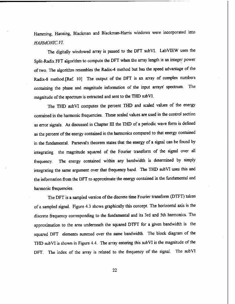
The DFT is a sampled version of the discrete time Fourier transform (DTFT) taken
of a sampled signal. Figure 4.3 shows graphically this concept. The horizontal axis is the
discrete frequency corresponding to the fundamental and its 3rd and 5th harmonics. The
approximation to the area underneath the squared DTFT for a given bandwidth is the
squared DFT elements summed over the same bandwidth. The block diagram of the
THD sub VI is shown in Figure 4.4. The array entering this subVI is the magnitude of the
DFT. The index of the array is related to the frequency of the signal. The subVI
22

X(f)
X(f)*W(f)
Discrete Fourier Transform of x(t)w(t)
Discrete Frequency
31 5t
Figure 4.3 Graphical Representation of Discrete Fourier Transform
23

itdatallTpggr iHMwwne
_^ m EH
&-$>—^>
a-1!^— :£>
031—=©>—pp>
^ÄSäfcJ^ THD r»sn
sü :: Harmonic Contentl
Figure 4.4 Block Diagram of THD subVI
24

determines the index containing the maximum value which corresponds to the fundamental
frequency. The index of the harmonic frequencies is the fundamental index multiplied by
the harmonic number. The array was split up into segments of twenty four elements
centered at the indexes of the fundamental and harmonic frequencies. Each sub array was
squared element by element and then summed to approximate a scaled value for the
energy contained within the desired frequencies. THD was then calculated by taking the
square root of the sum of the harmonic scaled values and dividing by the fundamental
value. The scaling factor cancels out in the calculation of THD. The THD and scaled
energy signals are then sent to the HARM AVE subVI.
The THD and error signals fluctuate making use of them for control difficult.
HARM AVE subVI performs a weighting average of THD and the error signals. A
block diagram of HARM AVE sub VI is shown in Figure 4.5. The weights were picked to
put more emphasis on the most recent values. In addition to the information provided for
averaging this subVI receives a trig (trigger input) and harm min (harmonic min) from the
control portion of HARMONIC.VI. Within this subVI a false trig input resets all the
averaging elements to their minimum values (harm min) for control purposes. The
information is displayed on the front panel and passed to the control section.
3. Control Development
Control development was the most challenging portion of the program. Lab VIEW
is a very powerful language for acquisition and processing but was not designed for
control applications. The intent of the control section was to use the energy signal
information from the processing section and derive the control signal weights mentioned in
Chapter HI. The control weights {S3,C3 ...Sh,Ch,...S15,C15} dictated the magnitude of
the sine and cosines wave forms that were added together in order to produce harmonic
25

r'^n^M^ t Jrfin h1^1^>4rin7i14i1n1^*1n?n3*1n^iwwi^«k^i.
■Wo li3^[h3^>*^n^1*^h1W«h3h^w*3h^WMrml1^112«^«4ffJO-iwa^-Jk h5H(H5W>5n™4&1W4i5n2W4i5n3™^^
h1H(h11*4h11irtl4h11n1W*l1n2W*M1r^)/[mnl4^ h1^13Wi13^1^13n1W^13r>?y*hl3n3^Mr^1«2«0*MJJ13-Hi £3 3- I' MW(h15^»h15n^1^15n1W4h15n2«*h15tOW^t»nl4ft2«3tn4jni15-1K'15mni19.1); THDHTHD"THTHDnW+THDnTn2+THDn2'W*THDnrn«)/(rHfl1«2w3«)4J: THDn4-THDn3jTHDn3-THDn2:THDn2-THDn1;THDn1-THDn;THDn.THD; Mr>Mi1n3ii1t*h1n2ii1n2*1n1Ji1n14i1i\Ji1n4i1; h3r»Wi3h3Tt>«1)^TI3-1)ttn34i3n21t>.1M^
«n«i5n3T6-1HH5mTa.1)«n346n?1t5-1Hi5r^ h5n14firf1S-1WÄm1l5l-1th5r>4i516-1Hi5rn1tS.1t h7r>44i7n3t7-1)»h7mt7!-1Ui7n3*7n«7-1)*h7rn1l7!-1)ii7n2-h7n11t7-1Ki7m1l7'-1).- h7n1-h7nH7-1hh7mfa7!-1th7r)-h7«(l7-1H>7m1t7!-1); . ^>-u> „uura„ h9nWfin?1S-1Hi9n.1l9-1 l«i*h9h2T^1hh9BW-1li>9n24i9n11t9-1Ki9inia-1); h9n1*9rflÖ-1H»nia-1lMr>*?(l9-1W*n1ia-1); M1nWi11n3TI11-1Hi'1'nTini.1lM1n3-h11n2ini-1Hi11m1t11l.1); h11n24>11n11l11-1Hi11mll11l-1th11n14i11nTl11-1Hi11nHni-1); h11n*int11—1W>11m"tl11l-1): h13i^13nni3-1)*13mT13-1)*13n3*13r^l13-1)^13<^13-1): hi 3n24i13r<1 H13—1 )*13mTI1 a-1 llil 3n14i13nH1 ^1 K>13mTI13-1); M3r*M3"(t1>-1Hh13nrtt13-1t „ , h15n4^>15n3tl15=1Ki15itr(na-1lti15n3*15n2nn5=1Hi15mTI15l-1J; h15n2^i15n1H15=1Hi15nmia-1lli15n14i15n1l15-1)«h15in1l19.1): M5n4i15H15-i1Hi15niTt19.lt
ButodOutieil
Figure 4.5 Block Diagram of HARM AVE subVI
26

canceling current signal which when injected into the network would reduce the energy
contained in its corresponding harmonic.
Theoretically since the sine and cosine functions are orthogonal the correction
signals proper phase and magnitude could be reached provided that the step size was small
enough. The weights needed to be varied one at a time and the response of the system
determined in order to see if the error signal had increased or decreased. Determining the
gradient of the error as a function of the changing weight would dictate the direction that
the weight would be varied. Once a minimum error signal was obtained the program
could move on to the next weight. Implementing a state machine to sequentially control
the distortion was decided to be the best approach. Figure 4.6 shows the state machine
approach to the problem. The coupling effect between harmonics made parallel correction
of harmonic to difficult.
Once the APLC was initialized and the control placed in auto the harmonic with
the largest error signal would be selected. The weight of the sine component of the
harmonic would start increasing. If the gradient were positive then the trigger would be
false and the sine weight would be deceased. The weight would be continually decreased
by a step size until the gradient turned positive and the trigger would become false. The
state would continue to execute while the trigger was true or until control was shifted to
off, hold or manual. The block diagram of the control case statements are shown in
Figure 4.7. This sequence continues until the correction sequence is passed and the
harmonic with the highest energy determined.
In practice, the gradient could not be easily used as the trigger because of
fluctuations in the error signals. This problem was overcome by assigning a variable to
store the lowest error signal value that occurs during each harmonics correction sequence
and cause the trigger to become false when the error signal reached this minimum error
27

Correction Sequence
Figure 4.6 State Machine
28

Figure 4.7 Control Case Statements
29

Signal plus some offset. This in essence searched for the proper weights by "swinging or
rocking" through the error signal. These are the trig (trigger input) and harm min
(harmonic min) signals previously mentioned in the data processing section. Figure 4.8
shows the block diagram of the subVI used to control the APLC as described above.
Each cycle the undated weights were sent to signal output section.
4. Signal Output
The AT-MIO-16F-5 data acquisition board has two analog output channels. Each
channel has its own buffer that different data sequences can be stored. The board was set
so that the conversion rate was constant. The output frequency could then be controlled
by varying the number of cycles in the data sequence. Arrays containing sinusoidal (both
cosine and sine) sequences, all of the same length, were generated in the SG subVI. The
arrays each contained a different number of cycles. The odd harmonics were to be
corrected therefore the arrays had the odd numbers as the number of cycles. Figure 4.9
shows the block diagram of the SG subVI. The weights developed in the control section
were passed to the SG subVI to be the amplitudes of the arrays. The arrays are added
element by element to develop the discrete distortion canceling signal. This signal is down
loaded to the specified I/O channel of the data acquisition board to become the input of
the current amplifier of the APLC.
30

^bit/Ml llljfil Jluftab5fa7fa9hlltl3b'
l>31h3>5Wl7ff^-51S^1H5>5)A7S^-51J7-J1h7>5)*ft7^7<^fl-31»5W1751h9<^l; ni-31h11>3M.751h11<-3^3*?(h13>3Hl7STh13<.3tn5Jlh15>3Hl75Th15<^lAi-10; tMh3m^3-1Wh3nwiria-1)>h3;^^ t7^h7m^7-1W7imtJrtt7!-1)>h7;»<[h9m^^ „,_ ,. . „ nH(h11m^ini11-1W1'n«<Jr(t11WB>MU13*l3nHn3nt13-1Mh13nminiia-ia>M3; t1W(h15nHfl5r(l1^-1Wh15m4u((1iia-1l>h15: h4v"fd!MW«rinrtd!—4L ,04ariocnwaoownh3>wa»5ntoi2)*^oomw
*N^ anwocwrihii>iwaooo5r(hii>i^ «»15^0.0001 Wa00O4nh15>1W0.MB5nM5>12l: H3iHh3t>3m>h3)*h3m1h3m<-h3I)t>-<)Wi3W
E3 h5nHh5Th5»h5H>5iinh5ro<46IP(h-1(*WtH-1t ES h7iHh71h7m>h7)*h7mrlh7in<Ji7inh-2Wi7,1H-2); SÄ h9Mh91h9p»h9Hi3m1h9m<«h9)r(^-3Wi31H-31; *^ h11nHh111h11i»h11Kinin^11m<-h11inh-4HmTH-4);
h13nHh1?1M3i«>h13>h13m1hian<4i13irth-5Hi131N^l; M5Mh151h15m>h15Wi15m1h15m<4i15)r(h-6H>15"W-«); «3nw3m1h3>h3mN31^"**U5m-t5m1h5>h5m}M51h5<-Wm); t7^«7m^h^h7m)«71h7<*7ml^9n«9m1K9>hSnl)«91h^<^aIll■ «11n«11iii1h11>h11m)*«111h11<-M1tnl3l3n«13m1h13>h13mH131h13<-*i13mI;
c3nPc3m1h3>h3m)«J1h3<4i3hljSiwäm1H5>h5i»)«51h5<4äiil: c7^«7m1h^h7mK71h7<4l7m)»^mc9m1h9>h9nl)K91h9<4l^m); clliiwIlitflhl^hllmlKlllhl^aillmlsiaBwiiaiifthl^hiamjKjIJlhl^-hiaBnt c15mc15m1h15>h15mKI5,,(h15<*l5ml: __ „ ^ „.,_ .m
^«5«Bncii-4)wt5^snc^i)rt^inh-i)^^-i)^iM^
.7*7*7H|h-W*-4M«7*7nib-2)U<cW c74c7*7TCh-2Wd>^c7*7n(h=^^ «Hi9*8l1|h-31l«c*^i9«iärtl^^
i^»11^1iri|hl4We*-^W««^"riff^)»*^ it cl1*11«(11rt|M)«<cii-2Mc11*1inib^W^
IUTPUTI
Figure 4.8 Block Diagram of Control subVI
31

Figure 4.9 Block Diagram of Signal Generating subVI
32

V. ACTIVE POWER LINE CONDITIONER TESTING AND RESULTS
A. TEST SETUP
The diagram shown in Figure 5.1 depicts the testing and measuring setup for the
APLC.
Oscilloscope
Active Power
Line Conditioner
Computer
Input
Output
Isolation Transformer
Voltage Source
Figure 5.1 Testing and Measuring Setup
A Copley 262V amplifier, controlled by the computer, was operated as a voltage
source. The amplifier was powered by the same source used by the current amplifier of
the APLC and connected as described in Chapter HI. The output voltage wave shape and
frequency of the amplifier are controlled by the computer. This is done by utilizing the
output of one of the data acquisition boards' D/A converters to drive the differential input
to the amplifier. The voltage supply section of HARMONIC. VI generates a sinusoidal data
array that is down loaded to the buffer associated with the specified I/O channel. The
33

conversion rate of the channels' D/A converter in conjunction with the number of periods
of data contained in the I/O buffer controls the output analog frequency at the desired
value. The Copley acts as an excellent low distortion voltage source with little associated
output impedance. In addition there is no need for frequency synchronization since the
computer is supplying the input sinusoidal signal for the amplifier. On the contrary, if
building power were used, the line impedance and slowly varying frequency of the bus
would need to be considered. For the purpose of this thesis, direct connection to the
building was not advantageous to "proof of principle", but would only interfere with the
accuracy by entering more unknowns unnecessarily.
The voltage source provided the power to the network as if it were supplied from
an uncorrupted stiff power grid. The distortion on a local bus is caused by the voltage
drop which occurs when the non-linear current drawn by the bus passes through the
transmission line. The line resistor (28Q) and the isolation transformer performed the part
of the transmission line.
The test equipment is powered by the wall outlet and therefore grounded. The
output of the Copley amplifiers need to be ungrounded; the test circuit was therefore
made to float. The Tektronix A6902B isolator isolated the ungrounded test circuit from
the test equipment. An additional reason for using this type of isolator was its ability to
step signals down. The voltage was reduced to meet the dynamic range of the data
acquisition boards' converters.
The non-linear load used in the test circuit was an inductor in series with a parallel
connected capacitor and resistor, all of which were driven by a phase controlled rectifier
(PCR). The test circuit is shown in Figure 5.2. The firing angle of the PCR is adjustable
by a precision potentiometer on the Variable AC/DC Supply Logic box. By adjusting the
firing angle, the amount of fundamental and harmonic current drawn were varied. [Ref. 11]
34

The ability to finely control the total amount of current drawn from the "weak" bus
allowed the for precise regulation the THD of the bus voltage.
LOGIC POWER SUPPLY
6 CHANNEL PULSE AMPLIFIER
VARIABLE AC/DC SUPPLY LOGIC
i Phase Controlled
Bridge Rectifier
21mH
25>iF
v. ssa
Figure 5.2 Non-linear Load
The following procedure is used for readying the test circuit for evaluation.
1. Energize computer, oscilloscope and isolator.
2. From the 208 VAC supply energize the rails of the amplifiers. Use the
variac and adjust the rail voltage to at least 150VDC.
3. Provide power to the PCR by energizing the Logic Power Supply, 6
Channel Pulse Amplifier and Variable AC/DC Supply Logic, in this order.
4. At the computer, execute the Lab VIEW program from Windows.
5. In Lab VIEW, execute the HARMONIC. VI.
6. Using the mouse start the VI running. The default values in the VI will
energize the voltage source and start acquisition of bus voltage data.
The VI takes a finite number of cycles to load the averaging elements. The
elements are fully loaded when the THD fluctuates less than one percent. Once the THD
is relatively stable the system is initialized and ready to be placed in auto for control to
35

begin. The APLC continues to correct the distortion until the control selector is shifted to
off or hold.
B. RESULTS
The trial run presented in this thesis started at a realistic distortion level of 12.5
percent. Figure 5.3 shows the initial distorted bus voltage wave form and the spectrum of
harmonic energy. The spectrum is automatically scaled in the vertical direction but fixed
in the horizontal direction. The x-axis starts at 100 Hz instead of the typical 0 Hz to cut
out the fundamental energy spike. The energy of the fundamental is many orders of
Figure 5.3 Bus Voltage and Energy Spectrum
36

magnitude larger than its harmonics and would overshadow their presence on the
spectrum.
The corrected bus voltage wave shape and its associated spectrum is shown in
Figure 5.4. The obvious notch that was present in the uncompensated wave shape has
been essentially eliminated. The compensated wave shape has significantly improved
towards the desired sinusoid. The spikes that are still present in the compensated voltage
wave shape are due primarily to the harmonics that were higher than the 15th which were
not corrected. The spectrum shows that the uncorrected harmonics' energy has increased
due mainly to the coupling effect of the non-linear load. The final THD was 3.0 percent.
Figure 5.4 APLC Corrected Bus Voltage and Energy Spectrum
37

The decrease in percent THD during the trial run is shown Figure 5.5. During
testing it became very apparent that the convergence rate to the proper control weights
and hence the drop of THD were sensitive to step size, averaging technique, data
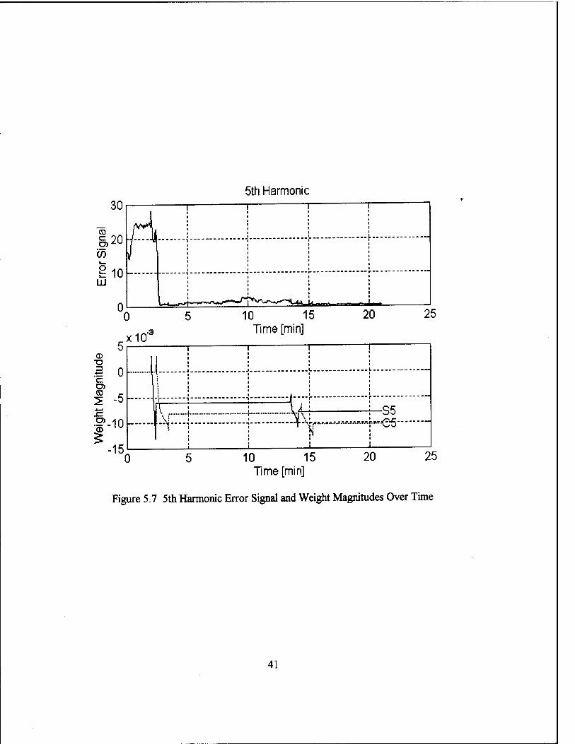
windowing and triggering levels. Figures 5.6 through 5.12 show the variations of each of
the corrected harmonics' error signal and weights over time. As explained in Chapter IV,
sequential control was used to remove the harmonic distortion. The harmonic with the
highest error signal is corrected first. The periods that the weights are not varying are the
times that some other weight is being changed either in the same harmonic or another with
a larger error signal. At times when the weights of a particular harmonic are not being
changed yet its' error signal is increasing, Figure 5.8 through 5.12, shows the significant
amount of coupling that exists between harmonics. As expected the weights were
converging on unique values depending of the network topology.
38

APLC Correction of Total Harmonic Distortion 14
12-1 o
| 10 b u '§ 8 E en
= 4 u ^_ 0_ Ä
0 0
1 _,
i ! i
10 15 Time [min]
20 25
Figure 5.5 Percent THD of Bus Voltage Over Time
39

30
CO c 20
HI 10-
0 0
3rd Harmonic
10 15 Time [min]
20
J. -C3
-S3
10 15 Time [min]
20 25
Figure 5.6 3rd Harmonic Error Signal and Weight Magnitudes Over Time
40
.x10" a»
ä of c
^ -5
1-10
-15 0
5th Harmonic
10 15 Time [min]
..-U-\ N
10 15 Time [min]
20
25
-S5 -€■5 -i
25
Figure 5.7 5th Harmonic Error Signal and Weight Magnitudes Over Time
41

0.02
ZJ 0.01 £Z O) CO 5 0 4—> x: en CD
-0.01 5
-0.02 "0
■V«
7th Harmonic
10 15 Time [min]
a.T.r.r.Ä.T.T.n.T.T.ÄÄÄ.r. J: AL«.nn.7.r.r..i.7.T.R.T.<?.r. ä.W.S?. .T.R
10 15 Time [min]
-S7
*-€-7-
20
25
25
Figure 5.8 7th Harmonic Error Signal and Weight Magnitudes Over Time
42

0
15 x10 •3
CD ■o 3 10 c CO .-
■? o
-5 0
9th Harmonic
10 15 Time [min]
20
& :C9-
25
JfLs9
25 5 10 15 20 Time [min]
Figure 5.9 9th Harmonic Error Signal and Weight Magnitudes Over Time
43

0
0.015 <D
I 0.01 Co
<D
0.005 -
0 0
11th Harmonic
10 15 Time [min]
20
PiC1T
J t~
^511
10 15 Time [min]
20
25
25
Figure 5.10 11th Harmonic Error Signal and Weight Magnitudes Over Time
44

0
0.02 a» ■o 3
4—i 0.01 c D) 03 2 0 4—i .c CD -0.01 5
-0.02 0
13th Harmonic
10 15 Time [min]
•A- lU
10 15 Time [min]
20
^■ets-
-S13
20
25
25
Figure 5.11 13th Harmonic Error Signal and Weight Magnitudes Over Time
45

,x10"
■o
a of c at CD
-5-
§-10h
■15
15th Harmonic
10 15 Time [min]
20
•C15
-&15-
25
0 5 10 15 20 25 Time [min]
Figure 5.12 15th Harmonic Error Signal and Weight Magnitudes Over Time
46

VL CONCLUSIONS AND RECOMMENDATIONS
A. CONCLUSIONS
The main goal of this thesis was to prove that THD of a local bus could be
corrected using only the knowledge of the local bus voltage. To this end, the results
presented in Chapter V show that the APLC, controlled solely from information derived
from the bus voltage, reasonable reduced the THD at the bus. The shortcoming indicated
by the results was the length of time that the algorithm took in order to come up with the
correct weights.
A secondary goal of the thesis was to create an optimal algorithm for determining
the control weights. The coupling that existed between harmonics led to a sequential
approach. This significantly contributed to the time required to reduce the THD. Since
both the phase and magnitude of the correction signal were unknown, only one of the
orthogonal functions could be varied at a time; this dictated a sequential approach to each
harmonic which added additional time to the process. The algorithm presented in this
thesis gave the best results considering the coupling effects and the limitation of Lab VIEW
as a controller.
B. RECOMMENDATIONS
Implementation of this approach on a dedicated digital signal processor (DSP)
board, such as the TMS520C30, should be investigated. The versatility of the C
programming language and the capability of today's DSP boards would allow for easy
implementation and compactability of the process.
47

The time to reduce the THD could be improved if a prior knowledge of the
network was known. The changes in a distribution system topology is periodic to some
extent. A neural network could be trained for a given system to predict its impedance
matrix, thus providing a starting point to the APLC. Additionally, the APLC could be
used to collect the information for the neural network since it would require injecting
various currents and monitoring the corresponding changes in bus voltage to determine
this impedance matrix.
A unity power factor converter should be built to provide the power to the APLC.
This converter could be powered off the same bus. This would close the loop and
theoretically make it feasible to install this type of self-contained harmonic correction
device in to any system with only one tap-in point.
48

LIST OF REFERENCES
1. Grady, W.M., Noyola, A.H., and Samotyj, M. J., "Survey of Active Power Line Conditioning Methodologies," IEEEPES, Winter Meeting, Atlanta, GA February 4, 1990.
2. Henderson, R.D., and Rose, P.J., "Harmonics: The Effects on Power Quality and Transformers," IEEE Trans, on Ind. Apps., Vol. 30, No. 3., pp528-532, May/June 1994.
3. Mohan, N., Undeland, T., and Robins, W., Power Electronics, 2nd Edition, John WUey & Sons, Inc., New York, NY, 1995.
4. Reid, W.E., "Power Quality Issues-Standards and Guidelines," IEEE Trans, on Ind Apps., ppl08-115, June 1994.
5. Operating and Service Manual Models 232, 232V, 262, and 262V High Power Amplifier, Copley Controls Corp., Westwood, MA August 1993.
6. AT-MO-I6F-5 User Manual, National Instruments, Austin, TX, July 1993.
7. Ashton, R. W., Harmonic and Power Factor Correction By Means of Active Line Conditioners With Adaptive Estimation Control, Ph.D. Dissertation, Worcester Polytechnic Institute, Worchester, MA 1991.
8. DataStor Deskside Computer, Data Storage Marketing, Inc., Boulder, CO, 1993.
9. LabVIEWfor Windows User Manual, National Instruments, Austin, TX, December 1993.
10. LabVIEWAnalysis VIReference Manual, National Instruments, Austin, TX, August 1993.
11. Fisher, M.J., Power Electronics, PWS-KENT Publishing Co., Boston, MA 1991.
49

50

INITIAL DISTRIBUTION LIST
1. Defense Technical Information Center Cameron Station Alexandria, Virginia 22304-6145
2. Library, Code 52 Naval Postgraduate School Monterey, California 93943-5101
3. Chairman, Code EC Department of Electrical and Computer Engineering Naval Postgraduate School Monterey, California 93943-5121
4. Professor Robert W. Ashton, Code EC/Ah Department of Electrical and Computer Engineering Naval Postgraduate School Monterey, California 93943-5121
5. Professor Michael K. Shields, Code EC/SI Department of Electrical and Computer Engineering Naval Postgraduate School Monterey, California 93943-5121
6. Professor Gurnam S. Gill, Code EC/Gi Department of Electrical and Computer Engineering Naval Postgraduate School Monterey, California 93943-5121
7. Lt. Kevin Jones c/o Ted Kyle 2428 Hickory Valley Rd Chattanooga, Tennessee 37421-1721
51