Embed Size (px)
Citation preview

sensors
Article
Resonant Rectifier ICs for Piezoelectric EnergyHarvesting Using Low-Voltage DropDiode Equivalents
Amad Ud Din, Seneke Chamith Chandrathna and Jong-Wook Lee *
Department of Electronics Engineering, Information and Communication System-on-Chip (SoC) ResearchCenter, Kyung Hee University, Yongin 17104, Korea; [email protected] (A.U.D.);[email protected] (S.C.C.)* Correspondence: [email protected]; Tel.: +82-31-201-3730
Academic Editor: Vittorio M. N. PassaroReceived: 20 February 2017; Accepted: 17 April 2017; Published: 19 April 2017
Abstract: Herein, we present the design technique of a resonant rectifier for piezoelectric (PE) energyharvesting. We propose two diode equivalents to reduce the voltage drop in the rectifier operation,a minuscule-drop-diode equivalent (MDDE) and a low-drop-diode equivalent (LDDE). The diodeequivalents are embedded in resonant rectifier integrated circuits (ICs), which use symmetric bias-flipto reduce the power used for charging and discharging the internal capacitance of a PE transducer.The self-startup function is supported by synchronously generating control pulses for the bias-flipfrom the PE transducer. Two resonant rectifier ICs, using both MDDE and LDDE, are fabricated ina 0.18 µm CMOS process and their performances are characterized under external and self-powerconditions. Under the external-power condition, the rectifier using LDDE delivers an output powerPOUT of 564 µW and a rectifier output voltage VRECT of 3.36 V with a power transfer efficiency of68.1%. Under self-power conditions, the rectifier using MDDE delivers a POUT of 288 µW and a VRECTof 2.4 V with a corresponding efficiency of 78.4%. Using the proposed bias-flip technique, the powerextraction capability of the proposed rectifier is 5.9 and 3.0 times higher than that of a conventionalfull-bridge rectifier.
Keywords: AC-DC converters; energy harvesting; piezoelectric; rectifier
1. Introduction
There is increasing demand for autonomous sensing devices, deployed in various applications,such as medical, healthcare, and environmental monitoring [1]. To enable uninterrupted data gatheringfrom a large population of sensing devices, e.g., the Internet of Things (IoT), a long lifetime is critical.Although there are continued innovations in battery capacity, battery lifetime is still finite. To extend thelifetime of sensing devices, energy can be acquired from ambient sources. There exist various sourcesfrom which energy can be extracted, including thermal, solar, vibrations, and wind. Among thoseenergy sources, vibrations can provide a relatively large amount of energy through highly-efficientpiezoelectric (PE) transducers.
The equivalent electrical model of a PE transducer is represented as a sinusoidal current sourceIP(t) = IPsin(ωpt) in parallel with a capacitor Cp and a resistor Rp, where ωp = 2πfp is the angularfrequency. In general, Rp is very large during low-frequency transducer operation, and the open-circuitvoltage can be expressed as Vp = IP/ωpCp. The output of a PE transducer is alternating current (AC) and,thus, needs conversion to direct current (DC). The commonly used AC-DC converters are full-bridgerectifiers (FBRs) and voltage doubler rectifiers (VDRs). Both FBR and VDR deliver a similar maximumoutput power when ideal diodes are used [2]. The operation of an FBR is well understood, which
Sensors 2017, 17, 901; doi:10.3390/s17040901 www.mdpi.com/journal/sensors
Sensors 2017, 17, 901 2 of 15
provides current for every half-cycle only after charging Cp to ±(VRECT + 2VD). Here, VRECT is therectified output voltage and VD is the diode voltage drop. The VDR provides current to the output onlyduring the positive half-cycle. In the negative half-cycle, a diode in parallel with the PE transducerprovides a path to discharge Cp to the ground. During the positive half-cycle, IP only needs to chargeCp from −VD to (VRECT + VD) before current can flow into the output.
In the rectifier, a commonly used figure-of-merit is the power transfer efficiency, which is definedas the ratio of the output power POUT to the input power PIN, which can be delivered by the PEtransducer. Rectifying a low voltage from a PE transducer may induce significant power losses due tothe diode voltage drop. An effective way to increase the efficiency of the rectifier is (1) reducing thediode’s voltage drop; and (2) increasing the input voltage by implementing the bias-flip strategy.
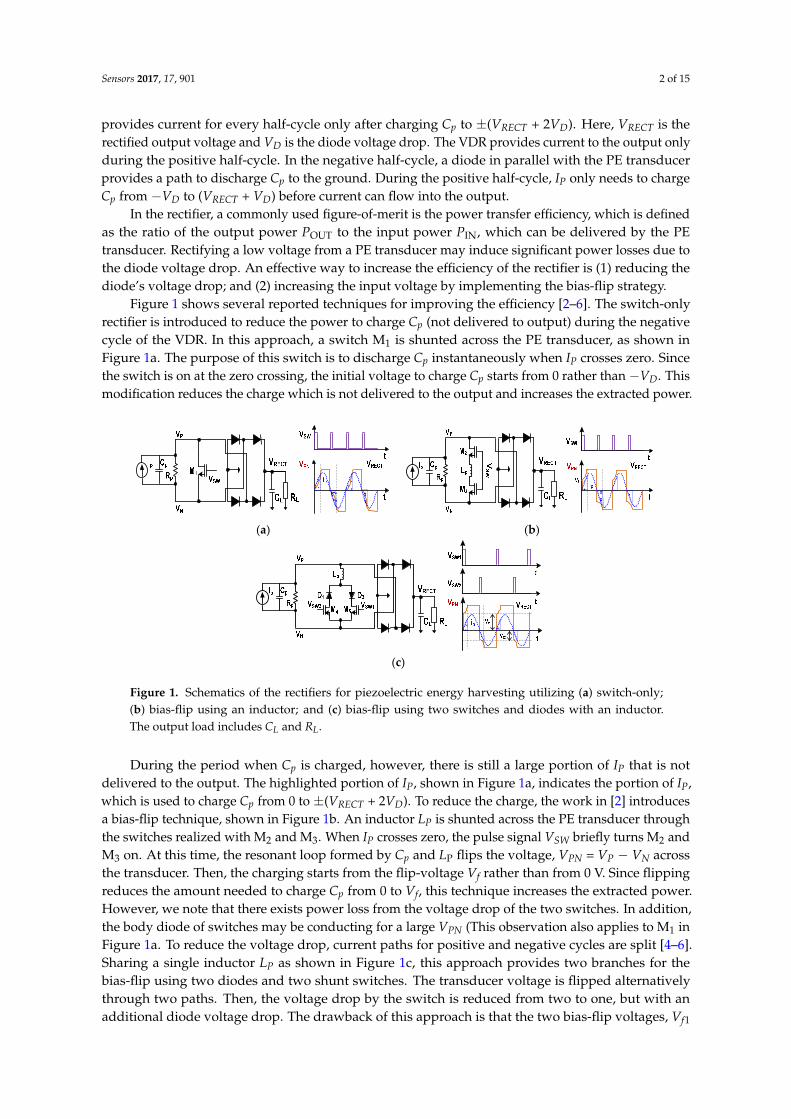
Figure 1 shows several reported techniques for improving the efficiency [2–6]. The switch-onlyrectifier is introduced to reduce the power to charge Cp (not delivered to output) during the negativecycle of the VDR. In this approach, a switch M1 is shunted across the PE transducer, as shown inFigure 1a. The purpose of this switch is to discharge Cp instantaneously when IP crosses zero. Sincethe switch is on at the zero crossing, the initial voltage to charge Cp starts from 0 rather than −VD. Thismodification reduces the charge which is not delivered to the output and increases the extracted power.
Sensors 2017, 17, 901 2 of 15
2VD). Here, VRECT is the rectified output voltage and VD is the diode voltage drop. The VDR provides current to the output only during the positive half-cycle. In the negative half-cycle, a diode in parallel with the PE transducer provides a path to discharge Cp to the ground. During the positive half-cycle, IP only needs to charge Cp from −VD to (VRECT + VD) before current can flow into the output.
In the rectifier, a commonly used figure-of-merit is the power transfer efficiency, which is defined as the ratio of the output power POUT to the input power PIN, which can be delivered by the PE transducer. Rectifying a low voltage from a PE transducer may induce significant power losses due to the diode voltage drop. An effective way to increase the efficiency of the rectifier is (1) reducing the diode’s voltage drop; and (2) increasing the input voltage by implementing the bias-flip strategy.
Figure 1 shows several reported techniques for improving the efficiency [2–6]. The switch-only rectifier is introduced to reduce the power to charge Cp (not delivered to output) during the negative cycle of the VDR. In this approach, a switch M1 is shunted across the PE transducer, as shown in Figure 1a. The purpose of this switch is to discharge Cp instantaneously when IP crosses zero. Since the switch is on at the zero crossing, the initial voltage to charge Cp starts from 0 rather than −VD. This modification reduces the charge which is not delivered to the output and increases the extracted power.
(a) (b)
(c)
Figure 1. Schematics of the rectifiers for piezoelectric energy harvesting utilizing (a) switch-only; (b) bias-flip using an inductor; and (c) bias-flip using two switches and diodes with an inductor. The output load includes CL and RL.
During the period when Cp is charged, however, there is still a large portion of IP that is not delivered to the output. The highlighted portion of IP, shown in Figure 1a, indicates the portion of IP, which is used to charge Cp from 0 to ±(VRECT + 2VD). To reduce the charge, the work in [2] introduces a bias-flip technique, shown in Figure 1b. An inductor LP is shunted across the PE transducer through the switches realized with M2 and M3. When IP crosses zero, the pulse signal VSW briefly turns M2 and M3 on. At this time, the resonant loop formed by Cp and LP flips the voltage, VPN = VP − VN across the transducer. Then, the charging starts from the flip-voltage Vf rather than from 0 V. Since flipping reduces the amount needed to charge Cp from 0 to Vf, this technique increases the extracted power. However, we note that there exists power loss from the voltage drop of the two switches. In addition, the body diode of switches may be conducting for a large VPN (This observation also applies to M1 in Figure 1a. To reduce the voltage drop, current paths for positive and negative cycles are split [4–6]. Sharing a single inductor LP as shown in Figure 1c, this approach provides two branches for the bias-flip using two diodes and two shunt switches. The transducer voltage is flipped alternatively through two paths. Then, the voltage drop by the switch is reduced from two to one, but with an additional diode voltage drop. The drawback of this approach is that
Figure 1. Schematics of the rectifiers for piezoelectric energy harvesting utilizing (a) switch-only;(b) bias-flip using an inductor; and (c) bias-flip using two switches and diodes with an inductor.The output load includes CL and RL.
During the period when Cp is charged, however, there is still a large portion of IP that is notdelivered to the output. The highlighted portion of IP, shown in Figure 1a, indicates the portion of IP,which is used to charge Cp from 0 to ±(VRECT + 2VD). To reduce the charge, the work in [2] introducesa bias-flip technique, shown in Figure 1b. An inductor LP is shunted across the PE transducer throughthe switches realized with M2 and M3. When IP crosses zero, the pulse signal VSW briefly turns M2 andM3 on. At this time, the resonant loop formed by Cp and LP flips the voltage, VPN = VP − VN acrossthe transducer. Then, the charging starts from the flip-voltage Vf rather than from 0 V. Since flippingreduces the amount needed to charge Cp from 0 to Vf, this technique increases the extracted power.However, we note that there exists power loss from the voltage drop of the two switches. In addition,the body diode of switches may be conducting for a large VPN (This observation also applies to M1 inFigure 1a. To reduce the voltage drop, current paths for positive and negative cycles are split [4–6].Sharing a single inductor LP as shown in Figure 1c, this approach provides two branches for thebias-flip using two diodes and two shunt switches. The transducer voltage is flipped alternativelythrough two paths. Then, the voltage drop by the switch is reduced from two to one, but with anadditional diode voltage drop. The drawback of this approach is that the two bias-flip voltages, Vf1

Sensors 2017, 17, 901 3 of 15
and Vf2 for positive and negative cycles, respectively, are different, i.e., Vf1 6= Vf2. This is becausethe impedance at VP and VN seen from the flipping path is different, and we observe asymmetricflipping in the waveform. The asymmetry results in fluctuation of the extracted power and increasedoutput ripple.
The diode voltage drop VD existing in the rectifier loop is the third reason for the low efficiency.The VD drop can be reduced by adding a bias voltage between the gate and drain terminal of atransistor [7]. To generate the bias voltages for a multi-stage rectifier, an extra bias distributor isrequired, which increases circuit complexity and the losses associated with it. In [3], an activediode, based on an op-amp with a pre-set DC offset, is used to reduce VD and the leakage current.Another method to reduce VD is by using a comparator-controlled switch [8]. This approach requiresapproximately one threshold voltage VTH plus two overdrive voltages to power up, limiting the inputvoltage for start-up to 1.2 V using a 0.35 µm CMOS process. Usually, the comparator is powered upfrom the output storage capacitor. If there is not enough voltage to power up, the comparator will notbe readily activated.
Herein, we propose two resonant rectifiers using low-voltage drop diode equivalents toovercome the limitations that exist in previous studies. We propose two diode equivalents,a minuscule-drop-diode equivalent (MDDE) and a low-drop-diode equivalent (LDDE), whicheffectively reduces the VD of the rectifying stage. The diode equivalents are efficiently combined with asymmetric and low-loss resonant loop to realize the bias-flip technique. Harnessing MDDE and LDDE,two resonant rectifier integrated circuits (ICs) having self-startup capabilities are designed. To improvethe efficiency under the self-power condition, the rectifier using MDDE includes synchronous bootstrappulse generators (SBPGs). The SBPG provides boosted bias-flipping pulses that are synchronizedwith the frequency of the PE transducer. Two resonant rectifier ICs using both MDDE and LDDE,are fabricated in a 0.18 µm CMOS process. The rectifier using LDDE shows measured POUT of564 µW under an external-powered condition with a corresponding efficiency of 68.1%. The rectifierusing MDDE shows enhanced efficiency under the self-powered condition. It delivers a POUT of288 µW with a corresponding efficiency of 78.4% and this result compares favorably with results fromprevious works.
2. Design
For an energy harvester, the capability for self-startup is one of the critical functions and severaltechniques have been reported [9–12]. In [9], the authors introduce a cold startup technique usinga transformer. For high voltage boosting, this approach needs a transformer with a large turn ratio,which can increase the overall size of the harvester. In [10], the authors propose a mechanical switchthat provides an instant power jerk to kick start the harvester. In [11], the authors present a low-voltagestartup technique using a VTH-tuned oscillator and a capacitor pass-on technique. Although a lowstartup voltage of 95 mV is achieved, the drawback is that this approach requires external programmingof a body voltage after fabrication. In [12], a charge pump with a switched body-biasing techniqueis presented. Since the body terminal of a transistor is connected to a high voltage when it is turnedoff, the reverse leakage is effectively suppressed. In these previous works, except [11], the self-startupfunction, which is vital to autonomous operation, is not fully supported. In this work, we embeda simple, yet efficient, approach for self-startup into the two resonant rectifiers.
2.1. Resonant Rectifier Using LDDE
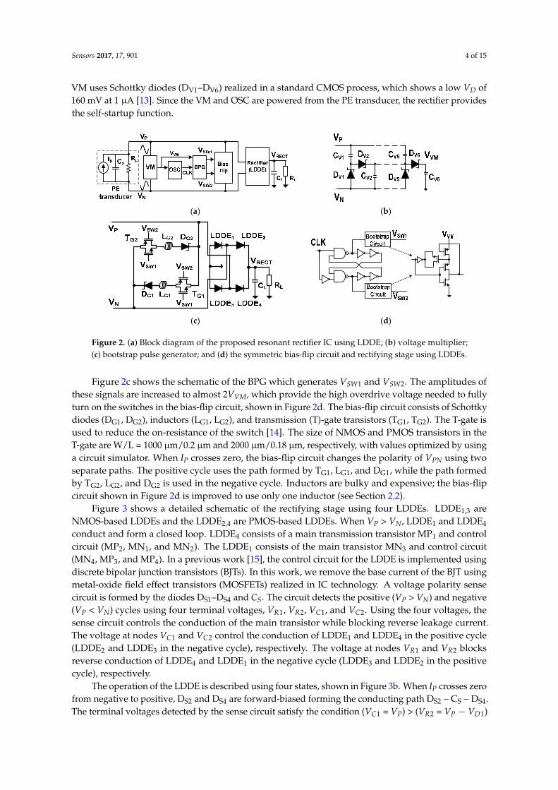
Figure 2a shows the block diagram of the resonant rectifier IC using LDDE. The rectifier consistsof a three-stage voltage multiplier (VM), an oscillator (OSC), a bootstrap pulse generator (BPG),a symmetric bias-flip circuit, and a full-bridge rectifying stage. The BPG provides the bootstrappedpulse signals VSW1 and VSW2 for the bias-flip circuit. The clock (CLK) signal for the BPG is generatedby the OSC with a frequency that can be tuned using a ring oscillator. The supply voltage of the OSCis driven by the output VVM of the voltage multiplier shown in Figure 2b. For efficient operation, the
Sensors 2017, 17, 901 4 of 15
VM uses Schottky diodes (DV1–DV6) realized in a standard CMOS process, which shows a low VD of160 mV at 1 µA [13]. Since the VM and OSC are powered from the PE transducer, the rectifier providesthe self-startup function.
Sensors 2017, 17, 901 4 of 15
which shows a low VD of 160 mV at 1 μA [13]. Since the VM and OSC are powered from the PE transducer, the rectifier provides the self-startup function.
(a) (b)
(c) (d)
Figure 2. (a) Block diagram of the proposed resonant rectifier IC using LDDE; (b) voltage multiplier; (c) bootstrap pulse generator; and (d) the symmetric bias-flip circuit and rectifying stage using LDDEs.
Figure 2c shows the schematic of the BPG which generates VSW1 and VSW2. The amplitudes of these signals are increased to almost 2VVM, which provide the high overdrive voltage needed to fully turn on the switches in the bias-flip circuit, shown in Figure 2d. The bias-flip circuit consists of Schottky diodes (DG1, DG2), inductors (LG1, LG2), and transmission (T)-gate transistors (TG1, TG2). The T-gate is used to reduce the on-resistance of the switch [14]. The size of NMOS and PMOS transistors in the T-gate are W/L = 1000 μm/0.2 μm and 2000 μm/0.18 μm, respectively, with values optimized by using a circuit simulator. When IP crosses zero, the bias-flip circuit changes the polarity of VPN using two separate paths. The positive cycle uses the path formed by TG1, LG1, and DG1, while the path formed by TG2, LG2, and DG2 is used in the negative cycle. Inductors are bulky and expensive; the bias-flip circuit shown in Figure 2d is improved to use only one inductor (see Section 2.2).
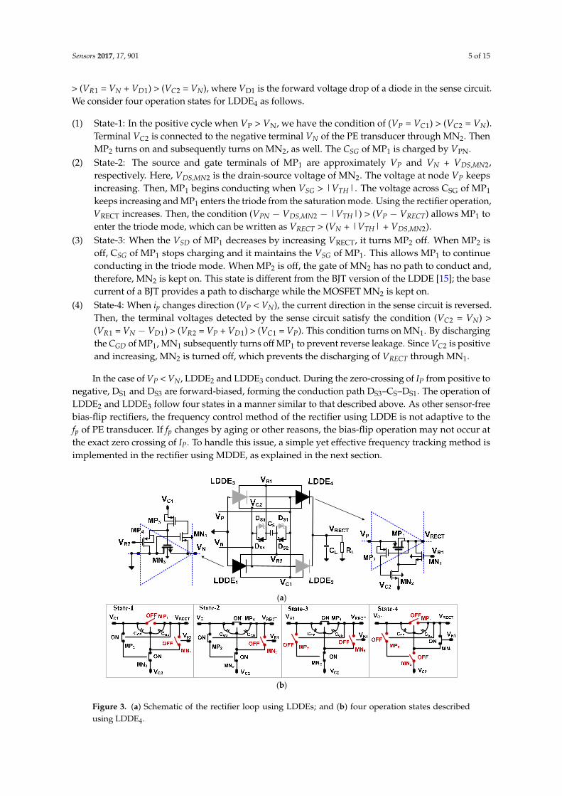
Figure 3 shows a detailed schematic of the rectifying stage using four LDDEs. LDDE1,3 are NMOS-based LDDEs and the LDDE2,4 are PMOS-based LDDEs. When VP > VN, LDDE1 and LDDE4 conduct and form a closed loop. LDDE4 consists of a main transmission transistor MP1 and control circuit (MP2, MN1, and MN2). The LDDE1 consists of the main transistor MN3 and control circuit (MN4, MP3, and MP4). In a previous work [15], the control circuit for the LDDE is implemented using discrete bipolar junction transistors (BJTs). In this work, we remove the base current of the BJT using metal-oxide field effect transistors (MOSFETs) realized in IC technology. A voltage polarity sense circuit is formed by the diodes DS1–DS4 and CS. The circuit detects the positive (VP > VN) and negative (VP < VN) cycles using four terminal voltages, VR1, VR2, VC1, and VC2. Using the four voltages, the sense circuit controls the conduction of the main transistor while blocking reverse leakage current. The voltage at nodes VC1 and VC2 control the conduction of LDDE1 and LDDE4 in the positive cycle (LDDE2 and LDDE3 in the negative cycle), respectively. The voltage at nodes VR1 and VR2 blocks reverse conduction of LDDE4 and LDDE1 in the negative cycle (LDDE3 and LDDE2 in the positive cycle), respectively.
The operation of the LDDE is described using four states, shown in Figure 3b. When IP crosses zero from negative to positive, DS2 and DS4 are forward-biased forming the conducting path DS2 – CS – DS4. The terminal voltages detected by the sense circuit satisfy the condition (VC1 = VP) > (VR2 = VP −
Figure 2. (a) Block diagram of the proposed resonant rectifier IC using LDDE; (b) voltage multiplier;(c) bootstrap pulse generator; and (d) the symmetric bias-flip circuit and rectifying stage using LDDEs.
Figure 2c shows the schematic of the BPG which generates VSW1 and VSW2. The amplitudes ofthese signals are increased to almost 2VVM, which provide the high overdrive voltage needed to fullyturn on the switches in the bias-flip circuit, shown in Figure 2d. The bias-flip circuit consists of Schottkydiodes (DG1, DG2), inductors (LG1, LG2), and transmission (T)-gate transistors (TG1, TG2). The T-gate isused to reduce the on-resistance of the switch [14]. The size of NMOS and PMOS transistors in theT-gate are W/L = 1000 µm/0.2 µm and 2000 µm/0.18 µm, respectively, with values optimized by usinga circuit simulator. When IP crosses zero, the bias-flip circuit changes the polarity of VPN using twoseparate paths. The positive cycle uses the path formed by TG1, LG1, and DG1, while the path formedby TG2, LG2, and DG2 is used in the negative cycle. Inductors are bulky and expensive; the bias-flipcircuit shown in Figure 2d is improved to use only one inductor (see Section 2.2).
Figure 3 shows a detailed schematic of the rectifying stage using four LDDEs. LDDE1,3 areNMOS-based LDDEs and the LDDE2,4 are PMOS-based LDDEs. When VP > VN, LDDE1 and LDDE4
conduct and form a closed loop. LDDE4 consists of a main transmission transistor MP1 and controlcircuit (MP2, MN1, and MN2). The LDDE1 consists of the main transistor MN3 and control circuit(MN4, MP3, and MP4). In a previous work [15], the control circuit for the LDDE is implemented usingdiscrete bipolar junction transistors (BJTs). In this work, we remove the base current of the BJT usingmetal-oxide field effect transistors (MOSFETs) realized in IC technology. A voltage polarity sensecircuit is formed by the diodes DS1–DS4 and CS. The circuit detects the positive (VP > VN) and negative(VP < VN) cycles using four terminal voltages, VR1, VR2, VC1, and VC2. Using the four voltages, thesense circuit controls the conduction of the main transistor while blocking reverse leakage current.The voltage at nodes VC1 and VC2 control the conduction of LDDE1 and LDDE4 in the positive cycle(LDDE2 and LDDE3 in the negative cycle), respectively. The voltage at nodes VR1 and VR2 blocksreverse conduction of LDDE4 and LDDE1 in the negative cycle (LDDE3 and LDDE2 in the positivecycle), respectively.
The operation of the LDDE is described using four states, shown in Figure 3b. When IP crosses zerofrom negative to positive, DS2 and DS4 are forward-biased forming the conducting path DS2 – CS – DS4.The terminal voltages detected by the sense circuit satisfy the condition (VC1 = VP) > (VR2 = VP − VD1)
Sensors 2017, 17, 901 5 of 15
> (VR1 = VN + VD1) > (VC2 = VN), where VD1 is the forward voltage drop of a diode in the sense circuit.We consider four operation states for LDDE4 as follows.
(1) State-1: In the positive cycle when VP > VN, we have the condition of (VP = VC1) > (VC2 = VN).Terminal VC2 is connected to the negative terminal VN of the PE transducer through MN2. ThenMP2 turns on and subsequently turns on MN2, as well. The CSG of MP1 is charged by VPN.
(2) State-2: The source and gate terminals of MP1 are approximately VP and VN + VDS,MN2,respectively. Here, VDS,MN2 is the drain-source voltage of MN2. The voltage at node VP keepsincreasing. Then, MP1 begins conducting when VSG > |VTH|. The voltage across CSG of MP1
keeps increasing and MP1 enters the triode from the saturation mode. Using the rectifier operation,VRECT increases. Then, the condition (VPN − VDS,MN2 − |VTH|) > (VP − VRECT) allows MP1 toenter the triode mode, which can be written as VRECT > (VN + |VTH| + VDS,MN2).
(3) State-3: When the VSD of MP1 decreases by increasing VRECT, it turns MP2 off. When MP2 isoff, CSG of MP1 stops charging and it maintains the VSG of MP1. This allows MP1 to continueconducting in the triode mode. When MP2 is off, the gate of MN2 has no path to conduct and,therefore, MN2 is kept on. This state is different from the BJT version of the LDDE [15]; the basecurrent of a BJT provides a path to discharge while the MOSFET MN2 is kept on.
(4) State-4: When ip changes direction (VP < VN), the current direction in the sense circuit is reversed.Then, the terminal voltages detected by the sense circuit satisfy the condition (VC2 = VN) >(VR1 = VN − VD1) > (VR2 = VP + VD1) > (VC1 = VP). This condition turns on MN1. By dischargingthe CGD of MP1, MN1 subsequently turns off MP1 to prevent reverse leakage. Since VC2 is positiveand increasing, MN2 is turned off, which prevents the discharging of VRECT through MN1.
In the case of VP < VN, LDDE2 and LDDE3 conduct. During the zero-crossing of IP from positive tonegative, DS1 and DS3 are forward-biased, forming the conduction path DS3–CS–DS1. The operation ofLDDE2 and LDDE3 follow four states in a manner similar to that described above. As other sensor-freebias-flip rectifiers, the frequency control method of the rectifier using LDDE is not adaptive to thefp of PE transducer. If fp changes by aging or other reasons, the bias-flip operation may not occur atthe exact zero crossing of IP. To handle this issue, a simple yet effective frequency tracking method isimplemented in the rectifier using MDDE, as explained in the next section.
Sensors 2017, 17, 901 5 of 15
VD1) > (VR1 = VN + VD1) > (VC2 = VN), where VD1 is the forward voltage drop of a diode in the sense circuit. We consider four operation states for LDDE4 as follows.
(1) State-1: In the positive cycle when VP > VN, we have the condition of (VP = VC1) > (VC2 = VN). Terminal VC2 is connected to the negative terminal VN of the PE transducer through MN2. Then MP2 turns on and subsequently turns on MN2, as well. The CSG of MP1 is charged by VPN.
(2) State-2: The source and gate terminals of MP1 are approximately VP and VN + VDS,MN2,
respectively. Here, VDS,MN2 is the drain-source voltage of MN2. The voltage at node VP keeps increasing. Then, MP1 begins conducting when VSG > |VTH|. The voltage across CSG of MP1 keeps increasing and MP1 enters the triode from the saturation mode. Using the rectifier operation, VRECT increases. Then, the condition (VPN − VDS,MN2 − |VTH|) > (VP − VRECT) allows MP1 to enter the triode mode, which can be written as VRECT > (VN + |VTH| + VDS,MN2).
(3) State-3: When the VSD of MP1 decreases by increasing VRECT, it turns MP2 off. When MP2 is off, CSG of MP1 stops charging and it maintains the VSG of MP1. This allows MP1 to continue conducting in the triode mode. When MP2 is off, the gate of MN2 has no path to conduct and, therefore, MN2 is kept on. This state is different from the BJT version of the LDDE [15]; the base current of a BJT provides a path to discharge while the MOSFET MN2 is kept on.
(4) State-4: When ip changes direction (VP < VN), the current direction in the sense circuit is reversed. Then, the terminal voltages detected by the sense circuit satisfy the condition (VC2 = VN) > (VR1 = VN − VD1) > (VR2 = VP + VD1) > (VC1 = VP). This condition turns on MN1. By discharging the CGD of MP1, MN1 subsequently turns off MP1 to prevent reverse leakage. Since VC2 is positive and increasing, MN2 is turned off, which prevents the discharging of VRECT through MN1.
In the case of VP < VN, LDDE2 and LDDE3 conduct. During the zero-crossing of IP from positive to negative, DS1 and DS3 are forward-biased, forming the conduction path DS3–CS–DS1. The operation of LDDE2 and LDDE3 follow four states in a manner similar to that described above. As other sensor-free bias-flip rectifiers, the frequency control method of the rectifier using LDDE is not adaptive to the fp of PE transducer. If fp changes by aging or other reasons, the bias-flip operation may not occur at the exact zero crossing of IP. To handle this issue, a simple yet effective frequency tracking method is implemented in the rectifier using MDDE, as explained in the next section.
(a)
(b)
Figure 3. (a) Schematic of the rectifier loop using LDDEs; and (b) four operation states described using LDDE4.
Figure 3. (a) Schematic of the rectifier loop using LDDEs; and (b) four operation states describedusing LDDE4.

Sensors 2017, 17, 901 6 of 15
2.2. Resonant Rectifier Using MDDE
Figure 4a shows the block diagram of the resonant rectifier using MDDE. The rectifier IC includestwo synchronous bootstrap pulse generators (SBPGs), dual voltage doublers, a symmetric bias-flipcircuit, and a rectifying stage using MDDE. Instead of using VM and OSC for frequency generation,the pulse signals VSW1 and VSW2 for the bias-flip circuit are directly derived from the PE transducer.For efficient bias-flipping, the VSW1 and VSW2 are bootstrapped by the SBPG, which is driven by theoutput VDBL from a voltage doubler. The dual voltage doublers are realized using the Schottky diodesDD1–DD4. Without an external power supply, the SBPG and doublers are driven by the PE transducer,realizing the self-startup function.
Figure 4b shows a schematic of the SBPG. The two SBPGs operate in a complementary manner,generating two opposite phase pulse signals, VSW1 and VSW2. In the SBPG, VP is compared with VNand the output of the comparator CMP1,2 drives the BPG. In this way, the voltages VSW1 and VSW2 forthe bias-flip circuit are generated in sync with the f p of the PE transducer. The comparator CMP1,2 isrealized using a differential amplifier with a latched load for increased gain. It achieves an open-loopgain of 35 dB by consuming 770 nA. Two diodes, DC1 and DC2, are used to prevent reverse leakagecurrent. By the BPG, the amplitudes of VSW1 and VSW2 are increased by about twice that of VDBL,which effectively flips the voltage across the nodes VP and VN.
Sensors 2017, 17, 901 6 of 15
2.2. Resonant Rectifier Using MDDE
Figure 4a shows the block diagram of the resonant rectifier using MDDE. The rectifier IC includes two synchronous bootstrap pulse generators (SBPGs), dual voltage doublers, a symmetric bias-flip circuit, and a rectifying stage using MDDE. Instead of using VM and OSC for frequency generation, the pulse signals VSW1 and VSW2 for the bias-flip circuit are directly derived from the PE transducer. For efficient bias-flipping, the VSW1 and VSW2 are bootstrapped by the SBPG, which is driven by the output VDBL from a voltage doubler. The dual voltage doublers are realized using the Schottky diodes DD1–DD4. Without an external power supply, the SBPG and doublers are driven by the PE transducer, realizing the self-startup function.
Figure 4b shows a schematic of the SBPG. The two SBPGs operate in a complementary manner, generating two opposite phase pulse signals, VSW1 and VSW2. In the SBPG, VP is compared with VN and the output of the comparator CMP1,2 drives the BPG. In this way, the voltages VSW1 and VSW2 for the bias-flip circuit are generated in sync with the fp of the PE transducer. The comparator CMP1,2 is realized using a differential amplifier with a latched load for increased gain. It achieves an open-loop gain of 35 dB by consuming 770 nA. Two diodes, DC1 and DC2, are used to prevent reverse leakage current. By the BPG, the amplitudes of VSW1 and VSW2 are increased by about twice that of VDBL, which effectively flips the voltage across the nodes VP and VN.
(a)
(b) (c)
Figure 4. (a) Block diagram of the proposed resonant rectifier IC using MDDE; (b) synchronous bootstrap pulse generator; and (c) bias-flip circuit and rectifying stage using MDDE.
To compensate the time delay between VSW1,2 and VPN, a delay line consisting of RDL and CDL is added. This allows fine tuning of the delay, which aligns the pulses VSW1 and VSW2 with the zero crossing of IP. Due to the power constraint for self-startup, the values of RDL and CDL, which depend on transducer parameters (RL, IP and fP), are externally controlled (Table 1). We perform circuit simulations and the results show that the fP from 100 to 800 Hz can be handled using this approach. The minimum delay determined by the comparator, a buffer, and BPG sets the 800 Hz as the maximum input frequency. Figure 4c shows the schematic of the bias-flip circuit and the rectifying stage using the MDDEs. To control the path for bias-flip, the Schottky diodes DG3 and DG4 are used. Using a single inductor LG3, two separate and symmetric paths are created for the positive (a path along TG4, LG3, and DG3) and negative (a path along TG3, LG3 and DG4) cycles. Compared to the bias-flip circuit for the rectifier using LDDE, the circuit for the MDDE is improved to use one shared inductor.
Figure 4. (a) Block diagram of the proposed resonant rectifier IC using MDDE; (b) synchronousbootstrap pulse generator; and (c) bias-flip circuit and rectifying stage using MDDE.
To compensate the time delay between VSW1,2 and VPN, a delay line consisting of RDL and CDLis added. This allows fine tuning of the delay, which aligns the pulses VSW1 and VSW2 with thezero crossing of IP. Due to the power constraint for self-startup, the values of RDL and CDL, whichdepend on transducer parameters (RL, IP and fP), are externally controlled (Table 1). We perform circuitsimulations and the results show that the fP from 100 to 800 Hz can be handled using this approach.The minimum delay determined by the comparator, a buffer, and BPG sets the 800 Hz as the maximuminput frequency. Figure 4c shows the schematic of the bias-flip circuit and the rectifying stage using theMDDEs. To control the path for bias-flip, the Schottky diodes DG3 and DG4 are used. Using a singleinductor LG3, two separate and symmetric paths are created for the positive (a path along TG4, LG3,and DG3) and negative (a path along TG3, LG3 and DG4) cycles. Compared to the bias-flip circuit forthe rectifier using LDDE, the circuit for the MDDE is improved to use one shared inductor.

Sensors 2017, 17, 901 7 of 15
Table 1. Values of the delay line depending on RL, IP, and fP.
fp (Hz) 200 300 400
RL (KΩ) 100 50 20 100 50 20 100 50 20
RDL (MΩ)/CDL (nF)
IP (µA)
200 8/1 8/1 10/1 8/1 8/1 8/1 8/1 8/1 8/1300 10/1 14/1 12/1 8/1 4/1.5 4/1.5 5/0.5 5/0.5 5/0.5400 10/1 14/1 14/1 8/1 8/1 5/1 8/0.5 8/0.5 3/1.2600 16/1 16/1 14/1 8/1.5 8/1.5 7/1.5 8/1 8/1 5/1.2
Figure 5 shows the operation of the rectifying stage using MDDEs. The bridge-type stage consistsof two PMOS and NMOS-based MDDEs. MDDE2,4 are PMOS-based MDDEs, where TP2 and TP4
are the main transmission transistors. MDDE1,3 are NMOS-based MDDEs, where TN1 and TN3 arethe main transistors. The control circuit, which consists of a diode and a transistor in each MDDE,reduces the VD of the main transistor via the deep-triode mode while blocking the reverse leakagecurrent. In the positive cycle (VP > VN), MDDE2 and MDDE3 close the loop, as shown in Figure 5a.The diode D2 is forward biased, which turns on N2. At this time, the gate of TP2 is connected toVN through N2, which turns on TP2. Since VN is negative, it also turns on P3 and D3. The VSG ofTP2 is determined by the voltage at the gate (VN + VDS,N2) and source (VRECT). With the condition(VRECT − VN − VDS,N2) > |VTH|, TP2 is turned on. The VGS of TN3 is determined by the voltage at thegate (VP − VSD,P3) and source (VRECT − VD,RL), where VSD,P3 and VD,RL are the source-drain voltageof P3 and the voltage drop across RL, respectively. With the condition (VP − VSD,P3 − VRECT + VD,RL)> VTH, the TN3 connects between VN and VRECT, closing the loop.
Sensors 2017, 17, 901 7 of 15
Figure 5 shows the operation of the rectifying stage using MDDEs. The bridge-type stage consists of two PMOS and NMOS-based MDDEs. MDDE2,4 are PMOS-based MDDEs, where TP2 and TP4 are the main transmission transistors. MDDE1,3 are NMOS-based MDDEs, where TN1 and TN3 are the main transistors. The control circuit, which consists of a diode and a transistor in each MDDE, reduces the VD of the main transistor via the deep-triode mode while blocking the reverse leakage current. In the positive cycle (VP > VN), MDDE2 and MDDE3 close the loop, as shown in Figure 5a. The diode D2 is forward biased, which turns on N2. At this time, the gate of TP2 is connected to VN through N2, which turns on TP2. Since VN is negative, it also turns on P3 and D3. The VSG of TP2 is determined by the voltage at the gate (VN + VDS,N2) and source (VRECT). With the condition (VRECT − VN − VDS,N2) > |VTH|, TP2 is turned on. The VGS of TN3 is determined by the voltage at the gate (VP − VSD,P3) and source (VRECT − VD,RL), where VSD,P3 and VD,RL are the source-drain voltage of P3 and the voltage drop across RL, respectively. With the condition (VP − VSD,P3 − VRECT + VD,RL) > VTH, the TN3 connects between VN and VRECT, closing the loop.
(a) (b)
Figure 5. Schematic of the rectifier loop using MDDE and operation during (a) positive and (b) negative cycles.
Table 1. Values of the delay line depending on RL, IP, and fP.
fp (Hz) 200 300 400 RL (KΩ) 100 50 20 100 50 20 100 50 20
RDL (MΩ)/CDL (nF)
IP (μA)
200 8/1 8/1 10/1 8/1 8/1 8/1 8/1 8/1 8/1 300 10/1 14/1 12/1 8/1 4/1.5 4/1.5 5/0.5 5/0.5 5/0.5 400 10/1 14/1 14/1 8/1 8/1 5/1 8/0.5 8/0.5 3/1.2 600 16/1 16/1 14/1 8/1.5 8/1.5 7/1.5 8/1 8/1 5/1.2
Next, we find the condition for TP2 and TN3 to operate in triode mode. In TP2, we observe that the source-drain voltage is VRECT − VP and the source-gate voltage is VRECT − (VN + VDS,N2). Therefore, the condition VPN >> (|VTH| + VDS,N2) allows deep-triode operation of TP2. For TN3, we observe that the drain-source voltage is VN − (VRECT − VD,RL) and the gate-source voltage is (VP − VSD,P3) − (VRECT − VD,RL). Then, the condition VPN >> (VTH + VSD,P3) allows deep-triode mode operation for TN2. In the negative cycle (VP < VN), D2 and D3 are reverse biased, and the voltage at the source terminal of N2 is VN > 0 (for P3, it is VP < 0). Therefore, both N2 and P3 are kept off and the reverse leakage through TP2 and TN3 is blocked. The operation of MDDE1 and MDDE4 in the negative cycle (VP < VN) can be similarly described, as shown in Figure 5b.
Figure 6 shows the comparison of VD of the LDDE and MDDE as a function of IP. The two RL values and the size of the main transistor are chosen to match the result in [15]. Since the control circuit does not fully turn on with small IP values, the results show that the VD of both diode
Figure 5. Schematic of the rectifier loop using MDDE and operation during (a) positive and (b)negative cycles.
Next, we find the condition for TP2 and TN3 to operate in triode mode. In TP2, we observethat the source-drain voltage is VRECT − VP and the source-gate voltage is VRECT − (VN + VDS,N2).Therefore, the condition VPN >> (|VTH| + VDS,N2) allows deep-triode operation of TP2. For TN3,we observe that the drain-source voltage is VN − (VRECT − VD,RL) and the gate-source voltage is(VP − VSD,P3) − (VRECT − VD,RL). Then, the condition VPN >> (VTH + VSD,P3) allows deep-triodemode operation for TN2. In the negative cycle (VP < VN), D2 and D3 are reverse biased, and the voltageat the source terminal of N2 is VN > 0 (for P3, it is VP < 0). Therefore, both N2 and P3 are kept off andthe reverse leakage through TP2 and TN3 is blocked. The operation of MDDE1 and MDDE4 in thenegative cycle (VP < VN) can be similarly described, as shown in Figure 5b.

Sensors 2017, 17, 901 8 of 15
Figure 6 shows the comparison of VD of the LDDE and MDDE as a function of IP. The two RLvalues and the size of the main transistor are chosen to match the result in [15]. Since the control circuitdoes not fully turn on with small IP values, the results show that the VD of both diode equivalentsincreases in the small IP range from 20 to 40 µA. When IP increases above 60 µA, VD increases withIP. The LDDE has a narrow window in the IP range from 30 to 40 µA. In the case of MDDE, the VD isbelow 50 mV in the IP range from 30 to 60 µA. In order to investigate the performance for differentPE transducer parameters, Figure 6b shows the comparison of VD of the LDDE and MDDE for thedifferent periphery. For a PE transducer having IP = 600 µA, the VD is 230 mV and 360 mV in caseof MDDE and LDDE having the same size, respectively. The results show that the MDDE showsan overall smaller VD than that of the LDDE over a broad range of IP. The LDDE use three extratransistors to control the on-resistance of the main conducting transistor. In the case of the MDDE,the control is achieved using a transistor and a diode, which makes it simple, with a low loss.
Sensors 2017, 17, 901 8 of 15
equivalents increases in the small IP range from 20 to 40 μA. When IP increases above 60 μA, VD increases with IP. The LDDE has a narrow window in the IP range from 30 to 40 μA. In the case of MDDE, the VD is below 50 mV in the IP range from 30 to 60 μA. In order to investigate the performance for different PE transducer parameters, Figure 6b shows the comparison of VD of the LDDE and MDDE for the different periphery. For a PE transducer having IP = 600 μA, the VD is 230 mV and 360 mV in case of MDDE and LDDE having the same size, respectively. The results show that the MDDE shows an overall smaller VD than that of the LDDE over a broad range of IP. The LDDE use three extra transistors to control the on-resistance of the main conducting transistor. In the case of the MDDE, the control is achieved using a transistor and a diode, which makes it simple, with a low loss.
(a) (b)
Figure 6. Comparison of the diode voltage drops as a function of IP for (a) different loads; and (b) periphery (W/L).
2.3. Loss Calculation
Figure 7 shows the key waveforms of the resonant rectifier. When the PE element starts providing IP, the rectifier enters a startup state. In this state, the BPG starts generating VSW1 and VSW2, which have amplitudes that increase with VPN. A steady-state is assumed after t1. Just before time t1, Cp is pre-recharged to −(VRECT + 2VD). At time t1, IP changes direction and the bias-flip operation allows the charging of Cp from Vf to (VRECT + 2VD) until t2. During this period, the output current Io starts flowing to the load. In the negative cycle, Cp is discharged from −Vf to −(VRECT + 2VD). The effectiveness of bias-flip is usually expressed using a flipping efficiency ηf, defined as:
2f RECT
fRECT
V V
V
(1)
The amount of charge QCp lost due to charging Cp during time interval [t1, t2] can be expressed as:
[ 2 ] [ 2 (2 1)]Cp RECT D f p RECT D RECT f pQ V V V C V V V C (2)
Next, we consider the charge lost across Rp in the time interval [t1, tπ]. Since VPN varies during the time interval, we consider two cases of charge losses, QRp1 during [t1, t2] and QRp2 during [t2, tπ], given by:
2
1 2 1 2
( ) ( )t tPN PN
Rp Rp Rp t tp p
V t V tQ Q Q dt dt
R R
(3)
During the time interval [t1, t2], Vf is inverted via a bias-flip. In this period, VPN(t) can be obtained by integrating IP(t) as:
0 50 100 150 20020
40
60
80
100
120
140
VD (
mV
)
IP (A)
RL = 80 k (LDDE)
RL = 113 k (LDDE)
RL = 80 k (MDDE)
RL = 113 k (MDDE)
0 100 200 300 400 500 6000
100
200
300
400
500
600
700
RL=113 K
VD(m
V)
IP(A)
W/L=1.5mm/3.5m (MDDE) W/L= 200m/1m (MDDE) W/L= 1.5mm/3.5m (LDDE) W/L= 200m/1m (LDDE)
Figure 6. Comparison of the diode voltage drops as a function of IP for (a) different loads;and (b) periphery (W/L).
2.3. Loss Calculation
Figure 7 shows the key waveforms of the resonant rectifier. When the PE element starts providingIP, the rectifier enters a startup state. In this state, the BPG starts generating VSW1 and VSW2, whichhave amplitudes that increase with VPN. A steady-state is assumed after t1. Just before time t1, Cp
is pre-recharged to −(VRECT + 2VD). At time t1, IP changes direction and the bias-flip operationallows the charging of Cp from Vf to (VRECT + 2VD) until t2. During this period, the output currentIo starts flowing to the load. In the negative cycle, Cp is discharged from −Vf to −(VRECT + 2VD).The effectiveness of bias-flip is usually expressed using a flipping efficiency ηf, defined as:
η f =Vf + VRECT
2VRECT(1)
The amount of charge QCp lost due to charging Cp during time interval [t1, t2] can be expressed as:
QCp = [VRECT + 2VD − Vf ]Cp = [VRECT + 2VD − VRECT(2η f − 1)]Cp (2)
Next, we consider the charge lost across Rp in the time interval [t1, tπ]. Since VPN varies duringthe time interval, we consider two cases of charge losses, QRp1 during [t1, t2] and QRp2 during [t2, tπ],given by:
QRp = QRp1 + QRp2 =∫ t2
t1
VPN(t)Rp
dt+∫ tπ
t2
VPN(t)Rp
dt (3)

Sensors 2017, 17, 901 9 of 15
During the time interval [t1, t2], Vf is inverted via a bias-flip. In this period, VPN(t) can be obtainedby integrating IP(t) as:
VPN(t) =1
Cp
∫ t
t1Ip sin ωt dt − Vf (t1) =
Ip
ωCp(cos ωt1 − cos ωt) − Vf (t1) (4)
Applying the boundary conditions Vf = VRECT(2η f − 1) and ωt1 ∼= 0, Equation (4) can beexpressed as:
VPN(t) = Vp(1− cos ωt) − VRECT(2η f − 1) (5)
where VP = IP/(ωpCp) is the open-circuit voltage. Using Equation (5), QRp1 is obtained as:
QRp1 =∫ t2
t1Vp(1−cos ωt)−VRECT(2η f−1)
Rpdt ∼= Vp
ωRp(ωt2 − sin ωt2) − VRECT
ωRp(2η f − 1)ωt2 (6)
Sensors 2017, 17, 901 9 of 15
1 1 11
1( ) sin ( ) (cos cos ) ( )
t pPN p f ft
p p
IV t I t dt V t t t V t
C C
(4)
Applying the boundary conditions (2 1)f RECT fV V and ωt1 0, Equation (4) can be
expressed as:
( ) (1 cos ) (2 1)PN p RECT fV t V t V (5)
where VP = IP/(ωpCp) is the open-circuit voltage. Using Equation (5), QRp1 is obtained as:
2
1 2 2 21
(1 cos ) (2 1)( sin ) (2 1)
t p RECT f p RECTRp ft
p p p
V t V V VQ dt t t t
R R R
(6)
Figure 7. Key waveforms of the resonant rectifier.
To find QRp2 during the time interval [t2, tπ], we need the value of ωt2 and, thus, use the following relationship:
sin p pp p p
dV dVI t C C
dt d t
(7)
Integrating Equation (7) over the time interval [t1, t2] when bias-flipping is performed, we obtain:
2 1 2 1( cos cos ) ( ) ( )p p pV t t V t V t (8)
The values of Vp can be obtained from the waveform, which are 1( ) p fV t V and
2( ) ( 2 )p RECT DV t V V . Then, Equation (8) can be written as:
12
2 2 21cos ( )p RECT D RECT f
p
V V V Vt
V
(9)
Using Equation (9), QRp2 is obtained as:
2 2
( 2 )( )RECT D
Rpp
V VQ t t
R
(10)
where /t .
Figure 7. Key waveforms of the resonant rectifier.
To find QRp2 during the time interval [t2, tπ], we need the value of ωt2 and, thus, use thefollowing relationship:
Ip sin ωt = CpdVp
dt= ωCp
dVp
dωt(7)
Integrating Equation (7) over the time interval [t1, t2] when bias-flipping is performed, we obtain:
Vp(− cos ωt2 + cos ωt1) = Vp(t2) − Vp(t1) (8)
The values of Vp can be obtained from the waveform, which are Vp(t1) = Vf andVp(t2) = (VRECT + 2VD). Then, Equation (8) can be written as:
t2 =1ω
cos−1(Vp − 2VRECT − 2VD + VRECT2η f
Vp) (9)
Using Equation (9), QRp2 is obtained as:
QRp2 =(VRECT + 2VD)
Rp(tπ − t2) (10)
where tπ = π/ω.

Sensors 2017, 17, 901 10 of 15
The total charge produced by the PE transducer in every cycle is given by:
Qtotal = 2Ip/ω = 2CpVp (11)
The theoretical extracted power POUT,calc from the PE transducer for every cycle is obtained bytaking the available charge Equation (11) minus the various loss terms given by Equations (2), (6)and (10):
POUT,calc = 2 fpVRECT(Qtotal − QCp − QRp1 − QRp2)
= 2 fpVRECT[2VpCp − [VRECT + 2VD − VRECT(2η f − 1)]Cp − [Vp
ωRp(ωt2 − sin ωt2) − VRECT
ωRp
(2η f − 1)ωt2] − [VRECT+2VDRp
(tπ − t2)](12)
3. Measured Results
The proposed rectifiers are fabricated in a one-poly six-metal 0.18 µm CMOS process with a top2 µm thick metal option. Figure 8 shows the chip microphotographs. The size of the rectifiers usingLDDE and MDDE are 0.26 mm × 0.19 mm and 0.51 mm × 0.46 mm, respectively. Figure 9 shows theexperimental setup to characterize the rectifier using the PE transducer.
Sensors 2017, 17, 901 10 of 15
The total charge produced by the PE transducer in every cycle is given by:
2 / 2total p p pQ I C V (11)
The theoretical extracted power POUT,calc from the PE transducer for every cycle is obtained by taking the available charge Equation (11) minus the various loss terms given by Equations (2), (6) and (10):
OUT,calc 1 2
2 2
2 2
2 ( )
2 [2 [ 2 (2 1)] [ ( sin )
2(2 1) ] [ ( )]
p RECT total Cp Rp Rp
p RECTp RECT p p RECT D RECT f p
p p
RECT Df
p
P f V Q Q Q QV V
f V V C V V V C t tR R
V Vt t t
R
(12)
3. Measured Results
The proposed rectifiers are fabricated in a one-poly six-metal 0.18 μm CMOS process with a top 2 μm thick metal option. Figure 8 shows the chip microphotographs. The size of the rectifiers using LDDE and MDDE are 0.26 mm × 0.19 mm and 0.51 mm × 0.46 mm, respectively. Figure 9 shows the experimental setup to characterize the rectifier using the PE transducer.
(a) (b)
Figure 8. Chip micrograph of the resonant rectifier ICs using (a) LDDE; and (b) MDDE.
Vibrating motor
PE transducer
SUS platePiezo ceramicAg electrode
Figure 9. Experimental setup.
The bimorph of the transducer has a thickness, a length and a width of 0.33, 75, and 20 mm, respectively [16]. Each layer consists of a stainless steel (SUS) plate, a piezo ceramic, and an Ag electrode. The PE transducer is mounted on a vibrating motor for mechanical excitement [17]. The transducer is excited using 200 Hz with an acceleration of 1.8 g. Under this condition, the theoretical optimum loading resistance of the PE transducer is 7.2 kΩ. Two wires attached to both sides of the transducer are interfaced with a test board containing the rectifiers. Table 2 shows the parameters used for the experiment. The value of the inductor for bias-flip is selected considering the trade-off between size and the Q-factor. The maximum current available from the transducer is 600 μA,
Figure 8. Chip micrograph of the resonant rectifier ICs using (a) LDDE; and (b) MDDE.
Sensors 2017, 17, 901 10 of 15
The total charge produced by the PE transducer in every cycle is given by:
2 / 2total p p pQ I C V (11)
The theoretical extracted power POUT,calc from the PE transducer for every cycle is obtained by taking the available charge Equation (11) minus the various loss terms given by Equations (2), (6) and (10):
OUT,calc 1 2
2 2
2 2
2 ( )
2 [2 [ 2 (2 1)] [ ( sin )
2(2 1) ] [ ( )]
p RECT total Cp Rp Rp
p RECTp RECT p p RECT D RECT f p
p p
RECT Df
p
P f V Q Q Q QV V
f V V C V V V C t tR R
V Vt t t
R
(12)
3. Measured Results
The proposed rectifiers are fabricated in a one-poly six-metal 0.18 μm CMOS process with a top 2 μm thick metal option. Figure 8 shows the chip microphotographs. The size of the rectifiers using LDDE and MDDE are 0.26 mm × 0.19 mm and 0.51 mm × 0.46 mm, respectively. Figure 9 shows the experimental setup to characterize the rectifier using the PE transducer.
(a) (b)
Figure 8. Chip micrograph of the resonant rectifier ICs using (a) LDDE; and (b) MDDE.
Vibrating motor
PE transducer
SUS platePiezo ceramicAg electrode
Figure 9. Experimental setup.
The bimorph of the transducer has a thickness, a length and a width of 0.33, 75, and 20 mm, respectively [16]. Each layer consists of a stainless steel (SUS) plate, a piezo ceramic, and an Ag electrode. The PE transducer is mounted on a vibrating motor for mechanical excitement [17]. The transducer is excited using 200 Hz with an acceleration of 1.8 g. Under this condition, the theoretical optimum loading resistance of the PE transducer is 7.2 kΩ. Two wires attached to both sides of the transducer are interfaced with a test board containing the rectifiers. Table 2 shows the parameters used for the experiment. The value of the inductor for bias-flip is selected considering the trade-off between size and the Q-factor. The maximum current available from the transducer is 600 μA,
Figure 9. Experimental setup.
The bimorph of the transducer has a thickness, a length and a width of 0.33, 75, and 20 mm,respectively [16]. Each layer consists of a stainless steel (SUS) plate, a piezo ceramic, and an Agelectrode. The PE transducer is mounted on a vibrating motor for mechanical excitement [17].The transducer is excited using 200 Hz with an acceleration of 1.8 g. Under this condition, thetheoretical optimum loading resistance of the PE transducer is 7.2 kΩ. Two wires attached to bothsides of the transducer are interfaced with a test board containing the rectifiers. Table 2 shows the

Sensors 2017, 17, 901 11 of 15
parameters used for the experiment. The value of the inductor for bias-flip is selected consideringthe trade-off between size and the Q-factor. The maximum current available from the transducer is600 µA, which corresponds to Vp = 4.34 V at 200 Hz. The equivalent circuit of a PE transducer can berepresented as a mechanical spring-mass coupled to an electrical circuit. The current in the primarymechanical side corresponds to proof mass relative velocity, which is determined by such parametersas PE material, dimension, and acceleration. By the electromechanical coupling factor, which describesthe effectiveness of the conversion from mechanical to electrical energies, the maximum currentis determined.
Table 2. Parameters for the experiment.
Parameters Value
fpCp
200 Hz110 nF
Rp 1 MΩLG1, LG2, LG3 1000 µH
CL 1 µFRL 10–200 KΩ
Figure 10 shows the measured result of the rectifier using LDDE. It shows the input voltage VPN,bootstrap pulse signals VSW1 and VSW2, and the output VRECT. The transient during self-startup isshown in the inset. When VPN is increased, the BPG starts generating VSW1 and VSW2. Then, VRECTstarts increasing and the steady-state condition is reached at about 20 s. After this time, VSW1 andVSW2 reach a value about twice that of the multiplier output and fully turn on the bias-flip circuit.
Sensors 2017, 17, 901 11 of 15
which corresponds to Vp = 4.34 V at 200 Hz. The equivalent circuit of a PE transducer can be represented as a mechanical spring-mass coupled to an electrical circuit. The current in the primary mechanical side corresponds to proof mass relative velocity, which is determined by such parameters as PE material, dimension, and acceleration. By the electromechanical coupling factor, which describes the effectiveness of the conversion from mechanical to electrical energies, the maximum current is determined.
Table 2. Parameters for the experiment.
Parameters Valuefp
Cp
200 Hz 110 nF
Rp 1 MΩ LG1, LG2, LG3 1000 μH
CL 1 μF RL 10–200 KΩ
Figure 10 shows the measured result of the rectifier using LDDE. It shows the input voltage VPN, bootstrap pulse signals VSW1 and VSW2, and the output VRECT. The transient during self-startup is shown in the inset. When VPN is increased, the BPG starts generating VSW1 and VSW2. Then, VRECT starts increasing and the steady-state condition is reached at about 20 s. After this time, VSW1 and VSW2 reach a value about twice that of the multiplier output and fully turn on the bias-flip circuit.
Figure 10. Measured waveforms of the resonant rectifier using LDDE.
Figure 11 shows the measured and calculated POUT and efficiency versus VRECT. We characterize the rectifier under external and self-power conditions. When it is externally powered, the VM provides power only to the BPG and the internal oscillator is turned off. The CLK frequency is supplied externally to match the fp of the PE transducer. By receiving the CLK, the BPG generates VSW1 and VSW2. The VRECT is measured with IP = 600 μA. Since VRECT depends on RL, it is varied from 10 to 200 kΩ, searching for an optimum value. When VRECT reaches 3.36 V, the measured peak POUT of 564 μW is achieved with an RL of 20 kΩ. The POUT,calc obtained using Equation (12) is 626 μW, which indicates that the power consumed by the control circuit is 62 μW. The maximum input power which can be delivered by the PE transducer is obtained as PIN = 2 Cpfp(Vp)2 = 828 μW. Using the definition for power transfer efficiency = POUT/PIN, we obtain 68.1%. Using the measured Vf of 1.53 V in Equation (1), a flipping efficiency ηf of 72.8% is achieved. Under the same PE input condition and with VD = 0.7 V, the maximum power that can be obtained using the FBR [2] is 190 μW. The results show that the rectifier using LDDE delivers three times higher POUT than that of the FBR.
Figure 10. Measured waveforms of the resonant rectifier using LDDE.
Figure 11 shows the measured and calculated POUT and efficiency versus VRECT. We characterizethe rectifier under external and self-power conditions. When it is externally powered, the VM providespower only to the BPG and the internal oscillator is turned off. The CLK frequency is suppliedexternally to match the fp of the PE transducer. By receiving the CLK, the BPG generates VSW1 andVSW2. The VRECT is measured with IP = 600 µA. Since VRECT depends on RL, it is varied from 10to 200 kΩ, searching for an optimum value. When VRECT reaches 3.36 V, the measured peak POUT
of 564 µW is achieved with an RL of 20 kΩ. The POUT,calc obtained using Equation (12) is 626 µW,which indicates that the power consumed by the control circuit is 62 µW. The maximum input powerwhich can be delivered by the PE transducer is obtained as PIN = 2 Cpfp(Vp)2 = 828 µW. Using thedefinition for power transfer efficiency = POUT/PIN, we obtain 68.1%. Using the measured Vf of 1.53 Vin Equation (1), a flipping efficiency ηf of 72.8% is achieved. Under the same PE input condition andwith VD = 0.7 V, the maximum power that can be obtained using the FBR [2] is 190 µW. The resultsshow that the rectifier using LDDE delivers three times higher POUT than that of the FBR.
Sensors 2017, 17, 901 12 of 15Sensors 2017, 17, 901 12 of 15
(a) (b)
Figure 11. Performance of the rectifier using LDDE: (a) output power versus output voltage; and (b) power transfer efficiency versus output voltage.
Under the self-power condition, a resistive voltage divider is placed at the output of the VM. The role of the divider is controlling the supply voltage of OSC, which determines the CLK. The voltage divider is tuned so that the CLK frequency is closely matched to the fp of PE transducer. The results show a POUT of 261 μW with a VRECT of 2.8 V.
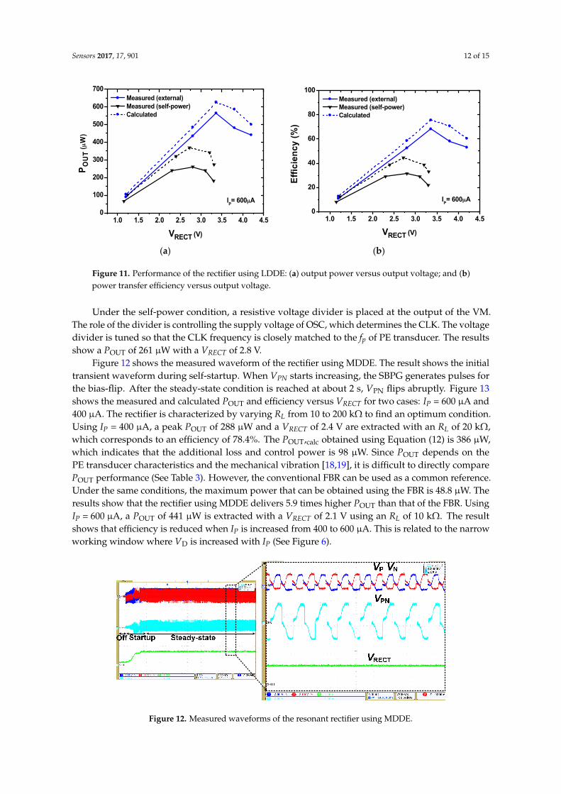
Figure 12 shows the measured waveform of the rectifier using MDDE. The result shows the initial transient waveform during self-startup. When VPN starts increasing, the SBPG generates pulses for the bias-flip. After the steady-state condition is reached at about 2 s, VPN flips abruptly. Figure 13 shows the measured and calculated POUT and efficiency versus VRECT for two cases: IP = 600 μA and 400 μA. The rectifier is characterized by varying RL from 10 to 200 kΩ to find an optimum condition. Using IP = 400 μA, a peak POUT of 288 μW and a VRECT of 2.4 V are extracted with an RL of 20 kΩ, which corresponds to an efficiency of 78.4%. The POUT,calc obtained using Equation (12) is 386 μW, which indicates that the additional loss and control power is 98 μW. Since POUT depends on the PE transducer characteristics and the mechanical vibration [18,19], it is difficult to directly compare POUT performance (See Table 3). However, the conventional FBR can be used as a common reference. Under the same conditions, the maximum power that can be obtained using the FBR is 48.8 μW. The results show that the rectifier using MDDE delivers 5.9 times higher POUT than that of the FBR. Using IP = 600 μA, a POUT of 441 μW is extracted with a VRECT of 2.1 V using an RL of 10 kΩ. The result shows that efficiency is reduced when IP is increased from 400 to 600 μA. This is related to the narrow working window where VD is increased with IP (See Figure 6).
Figure 12. Measured waveforms of the resonant rectifier using MDDE.
1.0 1.5 2.0 2.5 3.0 3.5 4.0 4.50
100
200
300
400
500
600
700
IP= 600A
P
OU
T (
W)
VRECT (V)
Measured (external) Measured (self-power) Calculated
1.0 1.5 2.0 2.5 3.0 3.5 4.0 4.50
20
40
60
80
100
IP= 600A
Eff
icie
ncy
(%
)
VRECT (V)
Measured (external) Measured (self-power) Calculated
Figure 11. Performance of the rectifier using LDDE: (a) output power versus output voltage; and (b)power transfer efficiency versus output voltage.
Under the self-power condition, a resistive voltage divider is placed at the output of the VM.The role of the divider is controlling the supply voltage of OSC, which determines the CLK. The voltagedivider is tuned so that the CLK frequency is closely matched to the fp of PE transducer. The resultsshow a POUT of 261 µW with a VRECT of 2.8 V.
Figure 12 shows the measured waveform of the rectifier using MDDE. The result shows the initialtransient waveform during self-startup. When VPN starts increasing, the SBPG generates pulses forthe bias-flip. After the steady-state condition is reached at about 2 s, VPN flips abruptly. Figure 13shows the measured and calculated POUT and efficiency versus VRECT for two cases: IP = 600 µA and400 µA. The rectifier is characterized by varying RL from 10 to 200 kΩ to find an optimum condition.Using IP = 400 µA, a peak POUT of 288 µW and a VRECT of 2.4 V are extracted with an RL of 20 kΩ,which corresponds to an efficiency of 78.4%. The POUT,calc obtained using Equation (12) is 386 µW,which indicates that the additional loss and control power is 98 µW. Since POUT depends on thePE transducer characteristics and the mechanical vibration [18,19], it is difficult to directly comparePOUT performance (See Table 3). However, the conventional FBR can be used as a common reference.Under the same conditions, the maximum power that can be obtained using the FBR is 48.8 µW. Theresults show that the rectifier using MDDE delivers 5.9 times higher POUT than that of the FBR. UsingIP = 600 µA, a POUT of 441 µW is extracted with a VRECT of 2.1 V using an RL of 10 kΩ. The resultshows that efficiency is reduced when IP is increased from 400 to 600 µA. This is related to the narrowworking window where VD is increased with IP (See Figure 6).
Sensors 2017, 17, 901 12 of 15
(a) (b)
Figure 11. Performance of the rectifier using LDDE: (a) output power versus output voltage; and (b) power transfer efficiency versus output voltage.
Under the self-power condition, a resistive voltage divider is placed at the output of the VM. The role of the divider is controlling the supply voltage of OSC, which determines the CLK. The voltage divider is tuned so that the CLK frequency is closely matched to the fp of PE transducer. The results show a POUT of 261 μW with a VRECT of 2.8 V.
Figure 12 shows the measured waveform of the rectifier using MDDE. The result shows the initial transient waveform during self-startup. When VPN starts increasing, the SBPG generates pulses for the bias-flip. After the steady-state condition is reached at about 2 s, VPN flips abruptly. Figure 13 shows the measured and calculated POUT and efficiency versus VRECT for two cases: IP = 600 μA and 400 μA. The rectifier is characterized by varying RL from 10 to 200 kΩ to find an optimum condition. Using IP = 400 μA, a peak POUT of 288 μW and a VRECT of 2.4 V are extracted with an RL of 20 kΩ, which corresponds to an efficiency of 78.4%. The POUT,calc obtained using Equation (12) is 386 μW, which indicates that the additional loss and control power is 98 μW. Since POUT depends on the PE transducer characteristics and the mechanical vibration [18,19], it is difficult to directly compare POUT performance (See Table 3). However, the conventional FBR can be used as a common reference. Under the same conditions, the maximum power that can be obtained using the FBR is 48.8 μW. The results show that the rectifier using MDDE delivers 5.9 times higher POUT than that of the FBR. Using IP = 600 μA, a POUT of 441 μW is extracted with a VRECT of 2.1 V using an RL of 10 kΩ. The result shows that efficiency is reduced when IP is increased from 400 to 600 μA. This is related to the narrow working window where VD is increased with IP (See Figure 6).
Figure 12. Measured waveforms of the resonant rectifier using MDDE.
1.0 1.5 2.0 2.5 3.0 3.5 4.0 4.50
100
200
300
400
500
600
700
IP= 600A
PO
UT
(
W)
VRECT (V)
Measured (external) Measured (self-power) Calculated
1.0 1.5 2.0 2.5 3.0 3.5 4.0 4.50
20
40
60
80
100
IP= 600A
Eff
icie
ncy
(%
)
VRECT (V)
Measured (external) Measured (self-power) Calculated
Figure 12. Measured waveforms of the resonant rectifier using MDDE.

Sensors 2017, 17, 901 13 of 15Sensors 2017, 17, 901 13 of 15
(a) (b)
Figure 13. Performance of the rectifier using MDDE for two IP values: (a) output power versus output voltage; and (b) power transfer efficiency versus output voltage.
Table 3 shows a performance comparison with previous works realized using IC technology. The work in [2] presents a resonant rectifier using the bias-flip technique. The bias-flip timing is controlled by a digital inverter delay line that can be programmed externally. Although the adjustable delay control provides flexibility to accommodate various PE transducers, self-startup is not supported. Further, the efficiency of 58% is rather low, which can be attributed to the voltage drop in bias-flip switches and rectifying stages. In [4], a passive differentiator is used to detect the IP polarity change. In this work, two separate paths are used to reduce the voltage drop for bias-flip. A relatively high POUT of 1230 μW is achieved under externally-powered conditions. The work in [6] proposes a parallel synchronized switch harvesting on inductor (P-SSHI) technique which extracts 48 μW. The result in [20] shows a high efficiency of 91%. Including [20], however, the results in [4,6] are based on discrete realization and not included for comparison.
Table 3. Performance comparison with previous works.
This Work
[2] [3] [21] [22] [23] [24] Rectifier (MDDE)
Rectifier (LDDE)
Tech. 0.18 μm 0.35 μm 0.18 μm 0.18 μm
0.35 μm 0.35 μm 0.25 μm
Type Bias-flip/diode
equivalent Bias-flip Active FBR S-SSHI
Energy Invest
Inductor-less
SSHI
VP (V) 2.89 4.34 2.8 2.8 2.2 2.6 2.5 4.9 f0 (Hz) 200 225 200 200 143 82 144
PE transducer Thrive K7520BP2 V22B Mide
Circuit model
Circuit model
V22B Mide
V22W Mide
V22B Mide
Self-power Y N N N Y N N Y VRECT (V) 2.4 3.36 3.2 2.78 3.6 3.7 1.0 3.9 POUT (μW) 288 564 53 81 74 52 35 136
Efficiency (%) 78.4 68.1 58 90 89.5 69 77 85
The work in [21] presents a series synchronized switch harvesting on inductor (S-SSHI) technique, which is applied to the conventional FBR. It shows a good efficiency of 89.5%. However, the results in [3,21] are obtained using an equivalent model of the PE transducer, therefore, its performance in a real environment is unknown. The work in [22] increases power extraction by investing energy from the battery to enhance the electromechanical coupling factor. The work in [23] presents a fully-integrated interface to a PE transducer which does not employ an inductor. By dynamically switching between parallel and series configurations of two PE transducers, this work achieves a peak efficiency of 77%. The work in [24] inserts an active diode in the resonant loop of
0.5 1.0 1.5 2.0 2.5 3.00
100
200
300
400
500
600
700
IP= 400A
IP= 600A
Calculated Measured
PO
UT
(W
)
VRECT (V)
0.5 1.0 1.5 2.0 2.5 3.00
20
40
60
80
100
IP= 400A
IP= 600A
Calculated Measured
Eff
icie
ncy
(
)
VRECT (V)
Figure 13. Performance of the rectifier using MDDE for two IP values: (a) output power versus outputvoltage; and (b) power transfer efficiency versus output voltage.
Table 3 shows a performance comparison with previous works realized using IC technology.The work in [2] presents a resonant rectifier using the bias-flip technique. The bias-flip timing iscontrolled by a digital inverter delay line that can be programmed externally. Although the adjustabledelay control provides flexibility to accommodate various PE transducers, self-startup is not supported.Further, the efficiency of 58% is rather low, which can be attributed to the voltage drop in bias-flipswitches and rectifying stages. In [4], a passive differentiator is used to detect the IP polarity change.In this work, two separate paths are used to reduce the voltage drop for bias-flip. A relatively highPOUT of 1230 µW is achieved under externally-powered conditions. The work in [6] proposes a parallelsynchronized switch harvesting on inductor (P-SSHI) technique which extracts 48 µW. The resultin [20] shows a high efficiency of 91%. Including [20], however, the results in [4,6] are based on discreterealization and not included for comparison.
Table 3. Performance comparison with previous works.
This Work[2] [3] [21] [22] [23] [24]Rectifier
(MDDE)Rectifier(LDDE)
Tech. 0.18 µm 0.35 µm 0.18 µm 0.18 µm 0.35 µm 0.35 µm 0.25 µm
Type Bias-flip/diodeequivalent Bias-flip Active FBR S-SSHI Energy Invest Inductor-less SSHI
VP (V) 2.89 4.34 2.8 2.8 2.2 2.6 2.5 4.9
f 0 (Hz) 200 225 200 200 143 82 144
PE transducer Thrive K7520BP2 V22B Mide Circuit model Circuit model V22B Mide V22W Mide V22B Mide
Self-power Y N N N Y N N Y
VRECT (V) 2.4 3.36 3.2 2.78 3.6 3.7 1.0 3.9
POUT (µW) 288 564 53 81 74 52 35 136
Efficiency (%) 78.4 68.1 58 90 89.5 69 77 85
The work in [21] presents a series synchronized switch harvesting on inductor (S-SSHI) technique,which is applied to the conventional FBR. It shows a good efficiency of 89.5%. However, the resultsin [3,21] are obtained using an equivalent model of the PE transducer, therefore, its performance in areal environment is unknown. The work in [22] increases power extraction by investing energy from thebattery to enhance the electromechanical coupling factor. The work in [23] presents a fully-integratedinterface to a PE transducer which does not employ an inductor. By dynamically switching betweenparallel and series configurations of two PE transducers, this work achieves a peak efficiency of

Sensors 2017, 17, 901 14 of 15
77%. The work in [24] inserts an active diode in the resonant loop of the SSHI circuit which allowsbias-flipping to occur at an optimal time without the need for complicated delay-tuning circuits. In theproposed rectifier using LDDE, we achieve an efficiency of 68.1% under the external-power condition.Under the self-power condition, the rectifier using MDDE delivers a POUT of 288 µW and a VRECTof 2.4 V. This corresponds to an efficiency of 78.4%. Although this efficiency number is lower thanthe results of [24], a POUT of 441 µW is extracted using IP = 600 µA, demonstrating the high powerextraction capability of the proposed work. The results indicate the improvement is achieved usingefficient bias-flipping with a low VD of the MDDE.
4. Conclusions
In this work, we presented an efficient rectifier design technique for PE energy harvesting.To reduce the voltage drop in the rectifier, two diode equivalents are proposed. The diode equivalentsare successfully embedded in two resonant rectifiers using the symmetric bias-flip technique.In addition, time synchronization of the bias-flip with the PE transducer is studied. Further, we proposea self-power boosted pulse generator that synchronously detects the zero crossing transition of the PEtransducer. The measured results show that the proposed rectifiers significantly increase the extractedpower and efficiency. The rectifier using LDDE delivers a POUT of 564 µW with a correspondingefficiency of 68.2%. The rectifier using MDDE delivers a POUT of 288 µW with a peak efficiency of78.4%. Compared to the conventional FBR, these results show that the rectifier using MDDE andLDDE achieves a power extraction capability enhanced by factors of 5.9 and three times, respectively.The results indicate that an improvement is achieved with the proposed diode equivalents. This resultcan play a valuable role in various sensing applications that demand energy harvesting to obtainauxiliary power for extended battery lifetime.
Acknowledgments: This research was supported by the Basic Science Research Program through the NationalResearch Foundation (NRF) of Korea (No. 2015R1A2A2A03004160).
Author Contributions: Amad Ud Din designed the resonant rectifiers and setup, performed the experimentalwork, and wrote the manuscript. Seneke Chamith Chandrathna supplied input to the rectifier operationand performed simulations. Jong-Wook Lee conceived the project, organized the paper content, and editedthe manuscript.
Conflicts of Interest: The authors declare no conflict of interest.
References
1. Roundy, S. Energy Scavenging for Wireless Sensor Networks with Special Focus on Vibrations; Kluwer AcademicPress: Dordrecht, The Netherlands, 2003.
2. Ramadass, Y.K.; Chandrakasan, A.P. An efficient piezoelectric energy harvesting interface circuit usinga bias-flip rectifier and shared inductor. IEEE J. Solid State Circuits 2010, 45, 189–204. [CrossRef]
3. Sun, Y.; Hieu, N.H.; Joeng, C.J.; Lee, S.G. An integrated high-performance active rectifier for piezoelectricvibration energy harvesting system. IEEE Trans. Power Electron. 2012, 27, 623–627. [CrossRef]
4. Krihely, N.; Ben-Yaakov, S. Self-contained resonant rectifier for piezoelectric sources under variablemechanical excitation. IEEE Trans. Power Electron. 2011, 26, 612–621. [CrossRef]
5. Lefeuvre, E.; Badel, A.; Richard, C.; Guyomar, D. A comparison between several vibration-poweredpiezoelectric generators for standalone systems. Sens. Actuators A Phys. 2005, 126, 405–416. [CrossRef]
6. Lu, S.; Boussaid, F. A highly efficient P-SSHI rectifier for piezoelectric energy harvesting. IEEE Trans.Power Electron. 2015, 30, 5364–5369. [CrossRef]
7. Umeda, T.; Yoshida, H.; Shuichi, S.; Fujita, F.; Suzuki, T.; Otaka, S. A 950-MHz rectifier circuit for sensornetwork tags with 10-m distance. IEEE J. Solid State Circuits 2006, 1, 35–41. [CrossRef]
8. Guo, S.; Lee, H. An efficiency-enhanced CMOS rectifier with unbalanced-bias comparators for transcutaneouspower high-current implants. IEEE J. Solid State Circuits 2009, 44, 1796–1804. [CrossRef]
9. Damascheke, J. Design of a low-input-voltage converter for the thermoelectric generator. IEEE Trans.Ind. Appl. 1997, 33, 1203–1207. [CrossRef]

Sensors 2017, 17, 901 15 of 15
10. Ramadass, Y.K.; Chandrakasan, A.P. A battery-less thermoelectric energy harvesting interface circuit with35 mV startup voltage. IEEE J. Solid State Circuits 2011, 46, 333–341. [CrossRef]
11. Chen, P.H.; Ishida, K.; Ikeuchi, K.; Zhang, X.; Honda, K.; Okuma, Y.; Ryu, Y.; Takamiya, M.; Sakurai, T.Startup techniques for 95 mV step-up converter by capacitor pass-on scheme and VTH-tuned oscillator withfixed charge programming. IEEE J. Solid State Circuits 2012, 47, 1252–1260. [CrossRef]
12. Kim, J.; Mok, P.K.T.; Kim, C. A 0.15 V-input energy harvesting charge pump with switching body biasingand adaptive dead-time for efficiency improvement. IEEE J. Solid State Circuits 2015, 50, 414–425. [CrossRef]
13. Lee, J.-W.; Lee, B.; Kang, H.B. A high sensitivity, CoSi2-Si Schottky diode voltage multiplier for UHF-bandpassive RFID tag chips. IEEE Microw. Wirel. Compon. Lett. 2008, 18, 830–832. [CrossRef]
14. Din, A.U.; Chung, D.; Park, D.; Lee, H.; Lee, J.-W. A high extraction self-controllable CMOS resonant rectifiercircuit for piezoelectric energy scavenging system. In Proceedings of the 2014 International SoC DesignConference (ISOCC), Jeju, Korea, 3–6 November 2014; pp. 40–41.
15. Karthikeyan, L.; Amrutur, B. Signal-powered low-drop-diode equivalent circuit for a full-wave bridgerectifier. IEEE Trans. Power Electron. 2012, 27, 4192–4201. [CrossRef]
16. Piezo-Electric Energy Harvesting THRIVE. Available online: http://www.thrive.co.jp./PDF/flyer_KINEZ_K7520BS2/BP2.pdf (accessed on 9 December 2016).
17. Tokyo Parts Industrial Co. Model FM34F vibration motor. Available online: http://gemart.co.kr/files/FM34F.pdf?PHPSESSID=3cc3e64e513e692acdf2ac974840f318 (accessed on 15 December 2016).
18. Caliò, R.; Rongala, U.; Camboni, D.; Milazzo, M.; Stefanini, C.; de Petris, G.; Oddo, C. Piezoelectric energyharvesting solutions. Sensors 2014, 14, 4755–4790. [CrossRef] [PubMed]
19. Dicken, J.; Mitcheson, P.D.; Stoianov, I.; Yeatman, E.M. Power-extraction circuits for piezoelectric energyharvesters in miniature and low-power applications. IEEE Trans. Power Electron. 2012, 27, 4514–4529.[CrossRef]
20. Lu, S.; Boussaid, F. An inductorless self-controlled rectifier for piezoelectric energy harvesting. Sensors 2015,15, 29192–29208. [CrossRef] [PubMed]
21. Do, X.-D.; Nguyen, H.H.; Han, S.K.; Lee, S.-G. A rectifier for piezoelectric energy harvesting system withseries synchronized switch harvesting inductor. In Proceedings of the 2013 IEEE Asian Solid-State CircuitsConference (A-SSCC), Singapore, 11–13 November 2013; pp. 10–13.
22. Kwon, D.; Rincón-Mora, G.A. A single-inductor 0.35 µm CMOS energy-investing piezoelectric harvester.IEEE J. Solid State Circuits 2014, 49, 2277–2291. [CrossRef]
23. Du, S.; Jia, Y.; Seshia, A.A. An efficient inductorless dynamically configured interface circuit for piezoelectricvibration energy harvesting. IEEE Trans. Power Electron. 2017, 32, 3595–3609. [CrossRef]
24. Wu, L.; Do, X.D.; Lee, S.G.; Ha, D.S. A self-powered and optimal SSHI circuit integrated with an activerectifier for piezoelectric energy harvesting. IEEE Trans. Circuits Syst. I Regul. Pap. 2017, 64, 537–549.[CrossRef]
© 2017 by the authors. Licensee MDPI, Basel, Switzerland. This article is an open accessarticle distributed under the terms and conditions of the Creative Commons Attribution(CC BY) license (http://creativecommons.org/licenses/by/4.0/).