Embed Size (px)
Citation preview
Contents
1. Product’s picture 2. Feature
3. Pins description
4. The parameters and mode of product
5. Block diagram
6. Debugging device
7. Characteristic of test
8. Test diagram
9. AT command set
Cortesia electronicca
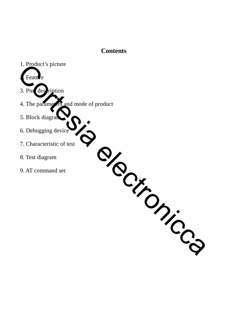
1. Product’s picture
Figure 1 A Bluetooth module
Cortesia electronicca
2. Feature Wireless transceiver
Sensitivity (Bit error rate) can reach -80dBm.
The change range of output’s power: -4 - +6dBm.
Function description (perfect Bluetooth solution)
Has an EDR module; and the change range of modulation depth: 2Mbps - 3Mbps.
Has a build-in 2.4GHz antenna; user needn’t test antenna.
Has the external 8Mbit FLASH
Can work at the low voltage (3.1V~4.2V). The current in pairing is in the range of 30~40mA.
The current in communication is 8mA.
Standard HCI Port (UART or USB)
USB Protocol: Full Speed USB1.1, Compliant With 2.0
This module can be used in the SMD.
It’s made through RoHS process.
The board PIN is half hole size.
Has a 2.4GHz digital wireless transceiver.
Bases at CSR BC04 Bluetooth technology.
Has the function of adaptive frequency hopping.
Small (27mm×13mm×2mm)
Peripherals circuit is simple.
It’s at the Bluetooth class 2 power level.
Storage temperature range: -40 ℃ - 85℃,work temperature range: -25 ℃ - +75℃
Any wave inter Interference: 2.4MHz,the power of emitting: 3 dBm.
Bit error rate: 0. Only the signal decays at the transmission link, bit error may be produced. For
example, when RS232 or TTL is being processed, some signals may decay.
Cortesia electronicca
Application fields:
Bluetooth Car Handsfree Device
Bluetooth GPS
Bluetooth PCMCIA , USB Dongle
Bluetooth Data Transfer
Software
CSR
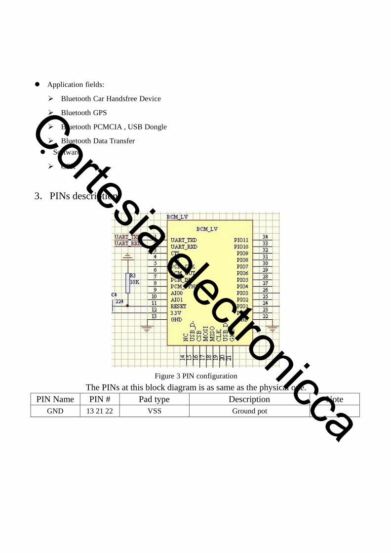
3.PINs description
Figure 3 PIN configuration The PINs at this block diagram is as same as the physical one.
PIN Name PIN # Pad type Description Note GND 13 21 22 VSS Ground pot
Cortesia electronicca
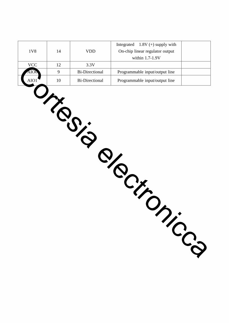
1V8
14
VDD Integrated 1.8V (+) supply with On-chip linear regulator output
within 1.7-1.9V
VCC 12 3.3V
AIO0 9 Bi-Directional Programmable input/output line
AIO1
10
Bi-Directional
Programmable input/output line Cortesia electronicca
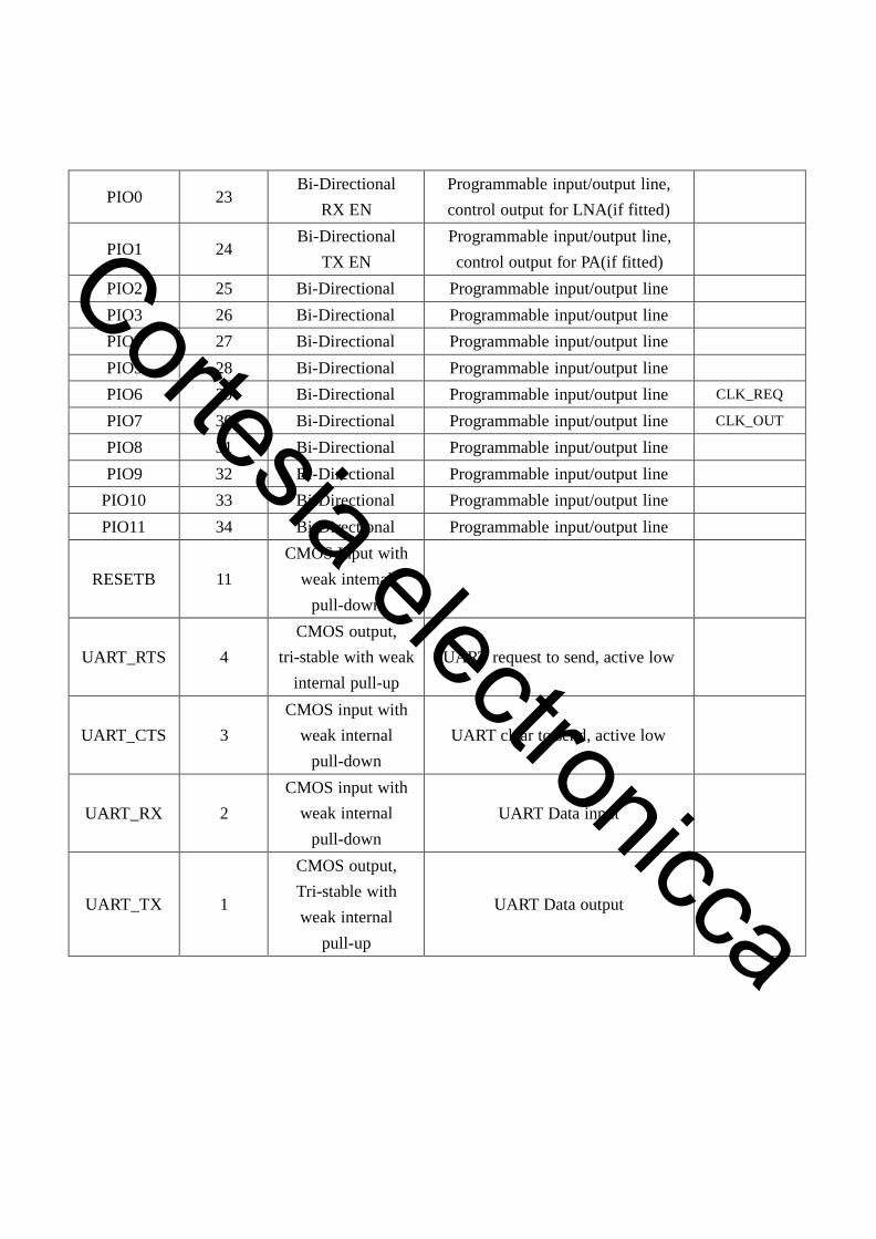
PIO0
23 Bi-Directional
RX EN Programmable input/output line, control output for LNA(if fitted)
PIO1
24
Bi-Directional TX EN
Programmable input/output line, control output for PA(if fitted)
PIO2 25 Bi-Directional Programmable input/output line
PIO3 26 Bi-Directional Programmable input/output line PIO4 27 Bi-Directional Programmable input/output line
PIO5 28 Bi-Directional Programmable input/output line PIO6 29 Bi-Directional Programmable input/output line CLK_REQ PIO7 30 Bi-Directional Programmable input/output line CLK_OUT PIO8 31 Bi-Directional Programmable input/output line
PIO9 32 Bi-Directional Programmable input/output line PIO10 33 Bi-Directional Programmable input/output line
PIO11 34 Bi-Directional Programmable input/output line
RESETB
11 CMOS Input with
weak intemal pull-down
UART_RTS
4 CMOS output,
tri-stable with weak internal pull-up
UART request to send, active low
UART_CTS
3 CMOS input with
weak internal pull-down
UART clear to send, active low
UART_RX
2 CMOS input with
weak internal pull-down
UART Data input
UART_TX
1
CMOS output, Tri-stable with weak internal
pull-up
UART Data output
Cortesia electronicca
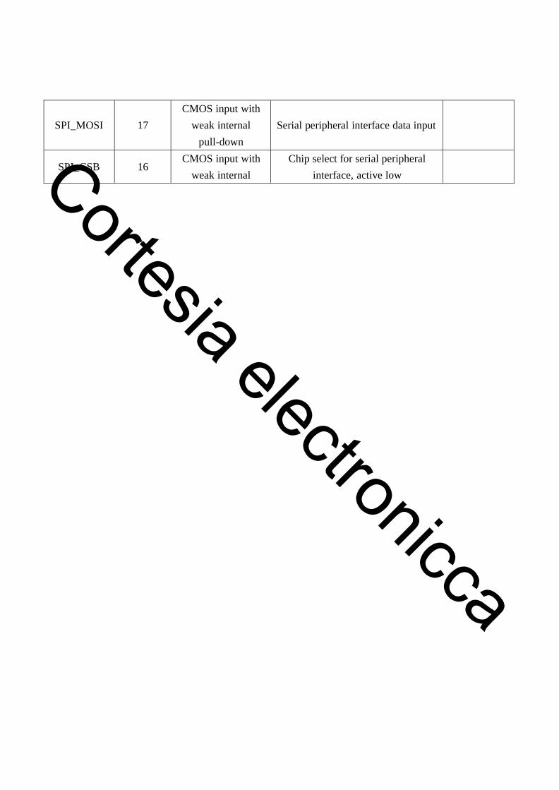
SPI_MOSI
17 CMOS input with
weak internal pull-down
Serial peripheral interface data input
SPI_CSB
16
CMOS input with weak internal
Chip select for serial peripheral interface, active low
Cortesia electronicca
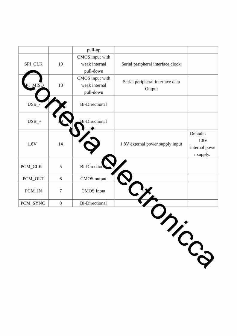
pull-up
SPI_CLK
19 CMOS input with
weak internal pull-down
Serial peripheral interface clock
SPI_MISO
18 CMOS input with
weak internal pull-down
Serial peripheral interface data
Output
USB_-
15
Bi-Directional
USB_+
20
Bi-Directional
1.8V
14
1.8V external power supply input
Default : 1.8V
internal powe r supply.
PCM_CLK
5
Bi-Directional
PCM_OUT 6 CMOS output
PCM_IN
7
CMOS Input
PCM_SYNC 8 Bi-Directional
Cortesia electronicca
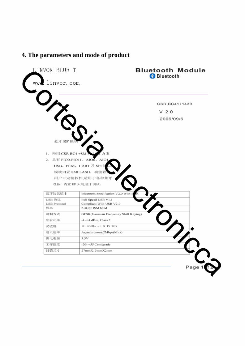
4. The parameters and mode of product
Cortesia electronicca
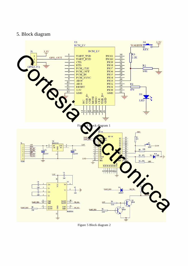
5. Block diagram Figure 5 Block diagram 1
Figure 5 Block diagram 2
Cortesia electronicca
HC-04/06 master device has a function of remembering the last paired slave device. As a master
device, it will search the last paired salve device until the connection is built. But if the WAKEUP bottom is pressed, HC-04/06 will lose the memory and research the new slave device.
6. Debugging device
6.1 Device
PC, hardware, 3G,3G Frequency Counter (SP3386), 3.15V DC power supply, Shielding,Bluetooth
Test box. 6.2 Software
7. Characteristic of test
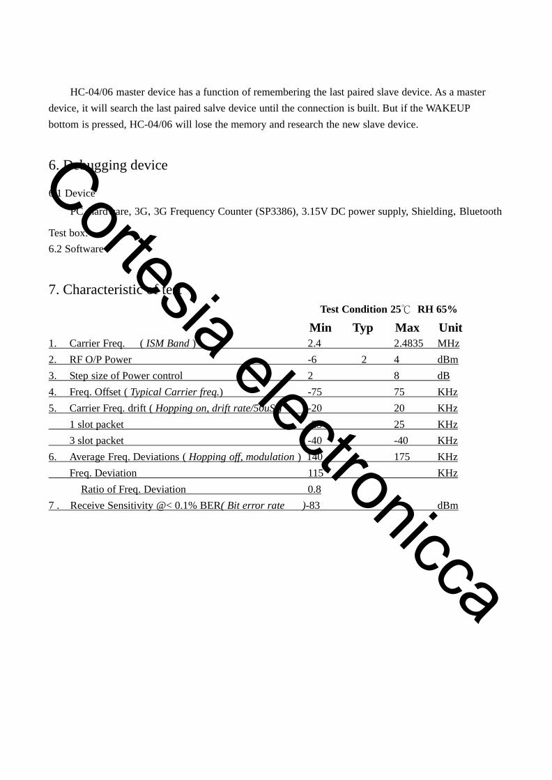
Test Condition 25℃ RH 65%
Min Typ Max Unit 1. Carrier Freq. ( ISM Band ) 2.4 2.4835 MHz 2. RF O/P Power -6 2 4 dBm 3. Step size of Power control 2 8 dB 4. Freq. Offset ( Typical Carrier freq.) -75 75 KHz 5. Carrier Freq. drift ( Hopping on, drift rate/50uS ) -20 20 KHz 1 slot packet -25 25 KHz 3 slot packet -40 -40 KHz 6. Average Freq. Deviations ( Hopping off, modulation ) 140 175 KHz Freq. Deviation 115 KHz
Ratio of Freq. Deviation 0.8 7 . Receive Sensitivity @< 0.1% BER( Bit error rate )-83 dBm
Cortesia electronicca
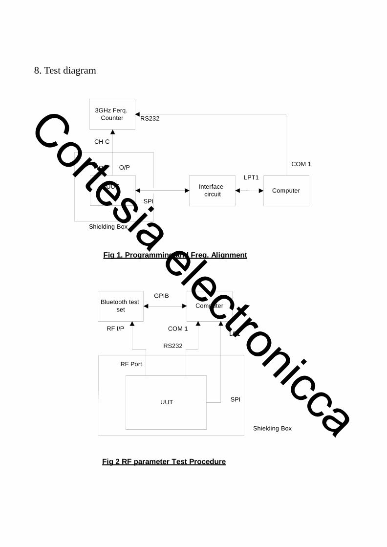
8. Test diagram
3GHz Ferq. Counter
RS232
CH C
RF O/P
UUT Interface circuit
LPT1
COM 1 Computer
SPI
Shielding Box
Fig 1. Programming and Freq. Alignment
Bluetooth test set
RF I/P
GPIB
COM 1
RS232
Computer
LP1
RF Port
UUT SPI
Shielding Box
Fig 2 RF parameter Test Procedure
Cortesia electronicca
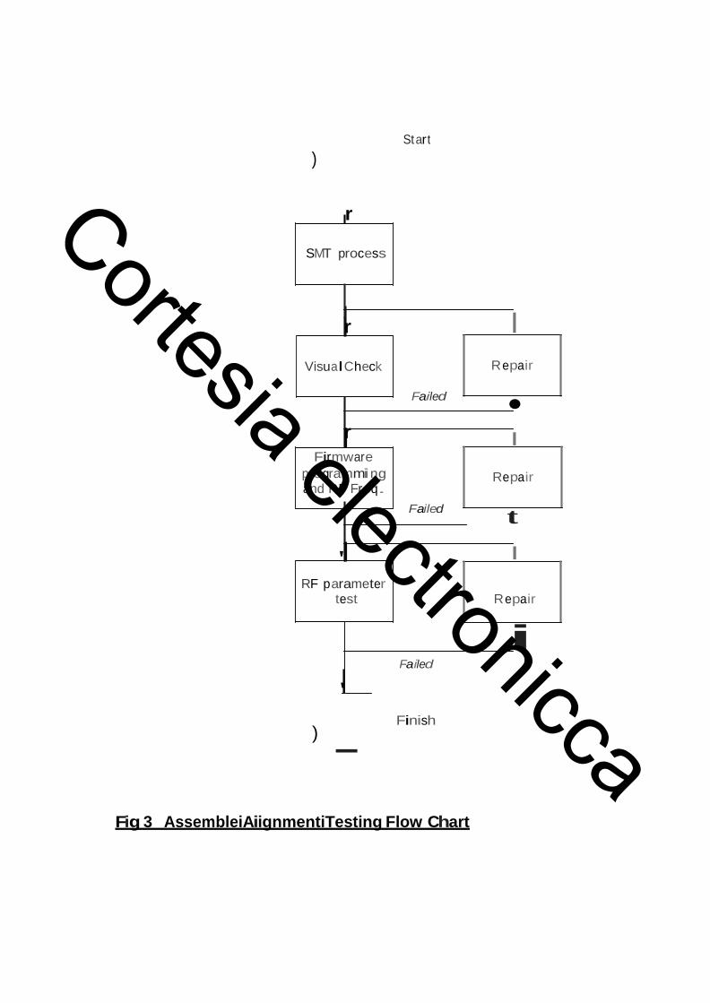
St art )
r
SMT process
r I
Visual Check R epair
Failed • r I
Firmware pro gramming Repair and RF Freq.
Failed t
' I RF p arameter
test R epair
i Failed
'
Finish ) -
Fig 3 AssembleiAiignmentiTesting Flow Chart
Cortesia electronicca
9.AT command set
The way to the AT command mode: supply power to the module, it will enter to the AT mode if it needn’t pair. The interval of command is about 1 second.
Default parameter: Baud rate:9600N81, ID: linvor, Password:1234 1. Test communication Send: AT (please send it every second) Back: OK
2. Reset the Bluetooth serial baud rate Send: AT+BAUD1 Back: OK1200 Send: AT+BAUD2 Back: OK2400 …… 1---------1200 2---------2400 3---------4800 4---------9600 (Default) 5---------19200 6---------38400 7---------57600 8---------115200 9---------230400 A---------460800 B---------921600 C---------1382400
PC can’t support the baud rate lager than 115200. The solution is: make the MCU have higher baud rate (lager than 115200) through programming, and reset the baud rate to low level through the AT command.
The baud rate reset by the AT command can be kept for the next time even though the power is cut off.
3. Reset the Bluetooth name Send: AT+NAMEname Back: OKname
Cortesia electronicca
Parameter name: Name needed to be set (20 characters limited) Example: Send: AT+NAMEbill_gates Back: OKname
Now, the Bluetooth name is reset to be “bill_gates” The parameter can be kept even though the power is cut off. User can see the new Bluetooth name
in PDA refresh service. (Note: The name is limited in 20 characters.)
4. change the Bluetooth pair password Send: AT+PINxxxx Back:OKsetpin
Parameter xxxx: The pair password needed to be set, is a 4-bits number. This command can be used in the master and slave module. At some occasions, the master module may be asked to enter the password when the master module tries to connect the slave module (adapter or cell-phone). Only if the password is entered, the successful connection can be built. At the other occasions, the pair can be finish automatically if the master module can search the proper slave module and the password is correct. Besides the paired slave module, the master can connect the other devices who have slave module, such as Bluetooth digital camera, Bluetooth GPS, Bluetooth serial printer etc. Example: Send: AT+PIN8888 Back: OKsetpin Then the password is changed to be 8888, while the default is 1234. This parameter can be kept even though the power is cut off.
5. No parity check ( The version, higher than V1.5, can use this command ) Send: AT+PN (This is the default value) Back: OK NONE
6. Set odd parity check ( The version, higher than V1.5, can use this command ) Send: AT+PO Back: OK ODD
7. Set even parity check( The version, higher than V1.5, can use this command ) Send: AT+PE Back: OK EVEN
Cortesia electronicca
8. Get the AT version Send: AT+VERSION Back: LinvorVl.n
Cortesia electronicca