Embed Size (px)
Citation preview

“Hello World” Nios II Hardware Lab:
DE10-Standard Development Kit
Version Date Editor Comments
1.0 20th June, 2017 Aanchal Sharma Created new manual for DE10_Standard, Tested and verified in Verilog

Contents:
Overview ................................................................................................................... 3
Lab Notes .................................................................................................................. 3
Quartus Installation .................................................................................................. 4
Design Flow ............................................................................................................... 5
Introduction to the DE10-Standard Development Kit ............................................... 7
Objective of hardware design for the “Hello World” lab .......................................... 7
HARDWARE DESIGN .................................................................................................. 8
Initial Setup ............................................................................................................... 8
Get started with Quartus ........................................................................................ 10
Building your Qsys based processor system ........................................................... 13
Building the top level design ................................................................................... 27
Adding the Nios II system into your design ............................................................ 33
SOFTWARE DESIGN ................................................................................................. 37
Creating the Software for the “Hello World” design .............................................. 37
Downloading the hardware image to the DE10-Standard Development Kit .......... 44
Lab Summary........................................................................................................... 49
Appendix A: Using Schematic Capture in place of writing
Verilog for the top
level module ........................................................................................................... 50
Appendix B: Merging the NIOS executable into the FPGA
configuration file
(Hardware Image) ................................................................................................... 54
Appendix C: Using Interrupt Service Routines (ISR) in a NIOS based system .......... 56

Overview This lab teaches you how to create an embedded system implemented in programmable logic using Altera’s “soft” Nios II processor. A soft processor is built from the programmable logic fabric and hence can be be easily modified to suit an application’s requirements whereas a hard processor is built from “hard” standard cells that cannot be changed without redesigning the chip. Soft processors can be built in any of Altera’s FPGA families, while hard processors can be found in Altera’s “SoC FPGA” device families such as Cyclone V SoC or Arria V SoC.. The Nios II processor is supported by a rich set of peripherals and “IP” blocks built that can be configured and connected to the processor using Altera’s QSys tool within the Quartus II design tool set. Altera also distributes the Nios II Software Build Tools (SBT) for Eclipse (for software development) within the Quartus development suite. This lab will show you how to install the DE10-Standard Development kit pin settings, design the processor-based hardware system, download it to the DE10-Standard Development Kit, and run a simple “Hello World” software program which displays text on your terminal. The lab is split into a Hardware Section and Software Section. You can skip the hardware section and move directly to the software section should you choose.
Lab Notes Many of the names that the lab asks you to choose for files, components, and other objects in this exercise must be spelled exactly as directed. This is necessary for consistency and to ensure that each step works properly in the lab, when creating your own systems, you can choose your own names if you use them consistently in your project. The directory paths shown in the figures are for Linux (forward slash directory delimiter). If you are using Windows, the paths will be shown with backslash directory delimiters.
Quartus Installation Quartus is Altera’s design tool suite. It serves several functions:
1. Design creation using HDL languages or schematics 2. System creation through the Qsys graphical interface 3. Generation and editing of constraints: timing, pin locations, physical location on die, IO voltage
levels 4. Synthesis of high level language into an FPGA netlist (“mapping” in FPGA terminology) 5. FPGA place and route (“fitting” in FPGA terminology) 6. Generation of design image (used to program FPGA, “assembly” in FPGA terminology) 7. Timing Analysis 8. Programming/download of design image into FPGA hardware 9. Debugging by insertion of debug logic (in-chip logic analyzer) 10. Interfaces to 3rd party tools such as simulators 11. Launching of Software Build Tools (Eclipse) for Nios II
To download Quartus, follow these instructions: Visit this site: http://dl.altera.com/?edition=web to download version 17.0 of Quartus II. Select version 17.0, Lite Edition and your PC’s operating system. For the smallest installation, and quickest download time, enter only the entries shown below.

Figure 1: Quartus download page
Follow the download instructions provided from the web page. No license is required to run Cyclone V FPGAs on the Quartus software.
Design Flow Unlike system development with hard processors, development with soft processors enables you to optimize the processor system to your application requirements and use the FPGA to add the performance and interfaces required by your system. This means that you need to know how to modify the processor system hardware; this may sound challenging but thanks to the Qsys graphical system design tool this is actually a relatively easy thing to do as we will demonstrate in this lab. Figure 2 illustrates how an overall system is integrated using the combination of the Qsys system integration tool, Quartus for mapping (FPGA terminology for synthesis), fitting (FPGA terminology for place and route), and the NIOS Software Build Tool (SBT) for software development.

Figure 2: Development Flow
The above diagram depicts the typical flow for Nios II system design. Hardware System definition is performed using Qsys; the resultant HDL files from the Qsys system are used by the Quartus II FPGA design software to map, fit and download the hardware image into the FPGA device. Quartus II also generates information that describes the configuration of the system designed in Qsys so that the Nios II SBT can be configured to create a software library that matches the hardware system and contains all the correct peripheral drivers.
Introduction to the DE10-Standard Development Kit
The DE10-Standard Development Kit, built around the Intel System-on-Chip (SoC) FPGA, combines the latest dual-core Cortex-A9 embedded cores with industry-leading programmable logic. Altera’s SoC integrates an ARM-based hard processor system (HPS) consisting of processor, peripherals and memory interfaces tied seamlessly with the FPGA fabric using a high-bandwidth interconnect backbone. The DE10-Standard development board includes hardware such as high-speed DDR3 memory, video and audio capabilities, Ethernet networking, and much more. In this lab, we will not use many of the interfaces, but there is a wealth of design examples and reference material demonstrating how to use these interfaces.

Figure 3: DE10-Standard Development Kit Features
Objective of hardware design for the “Hello World” lab For the simplest example, ‘a hello world lab’, the processor will load a program that prints “Hello World” to the screen. This requires a working processor to execute the code, on-chip memory to store the software executable, and a JTAG UART peripheral to send the “Hello World” text to a terminal. To make the lab a little bit more interesting and hardware-centric, we will utilize the push button switch and LED to allow interaction with the development kit by making the connection between the switch and LED directly in the FPGA fabric hardware. We will also use the processor to read and write the Switch and LED GPIO.
The lab hardware is constructed with the components shown below. Altera utilizes the Qsys network on chip interconnect to connect the master and slave devices together. To get a clear understanding of how quickly one can build an Embedded System using Qsys and the Quartus Design Software you will build the Nios II system entirely from scratch.

Figure 4: Nios II based system used in this lab
HARDWARE DESIGN
Initial Setup Should you want to skip the hardware design section, continue in the section called SOFTWARE DESIGN. Altera provides a starting point design to get the FPGA device pinouts associated with the development kits layout and your design via what is called the Baseline design. Navigate to Altera’s design store: https://cloud.altera.com/devstore Click on Design Examples.
Figure 5: Design Store
Once in Design Examples, filter by the Cyclone V family and Cyclone V SoC DE10-Standard Development kit.

Figure 6: Design Examples under Design Store
Select the Cyclone V SoC DE10-Standard Baseline Pinout
Figure 7: Cyclone V SoC DE10-Standard Baseline design Example Select the Download button and save the DE_Standard_10_Golden_Top.par design locally to your lab working directory (call the directory devkit_hello_world).
Get started with Quartus Now you are ready to get started designing hardware! Launch Quartus by double clicking the icon. Next you will launch the New Project Wizard from Quartus from the main panel or alternatively File New Project Wizard.
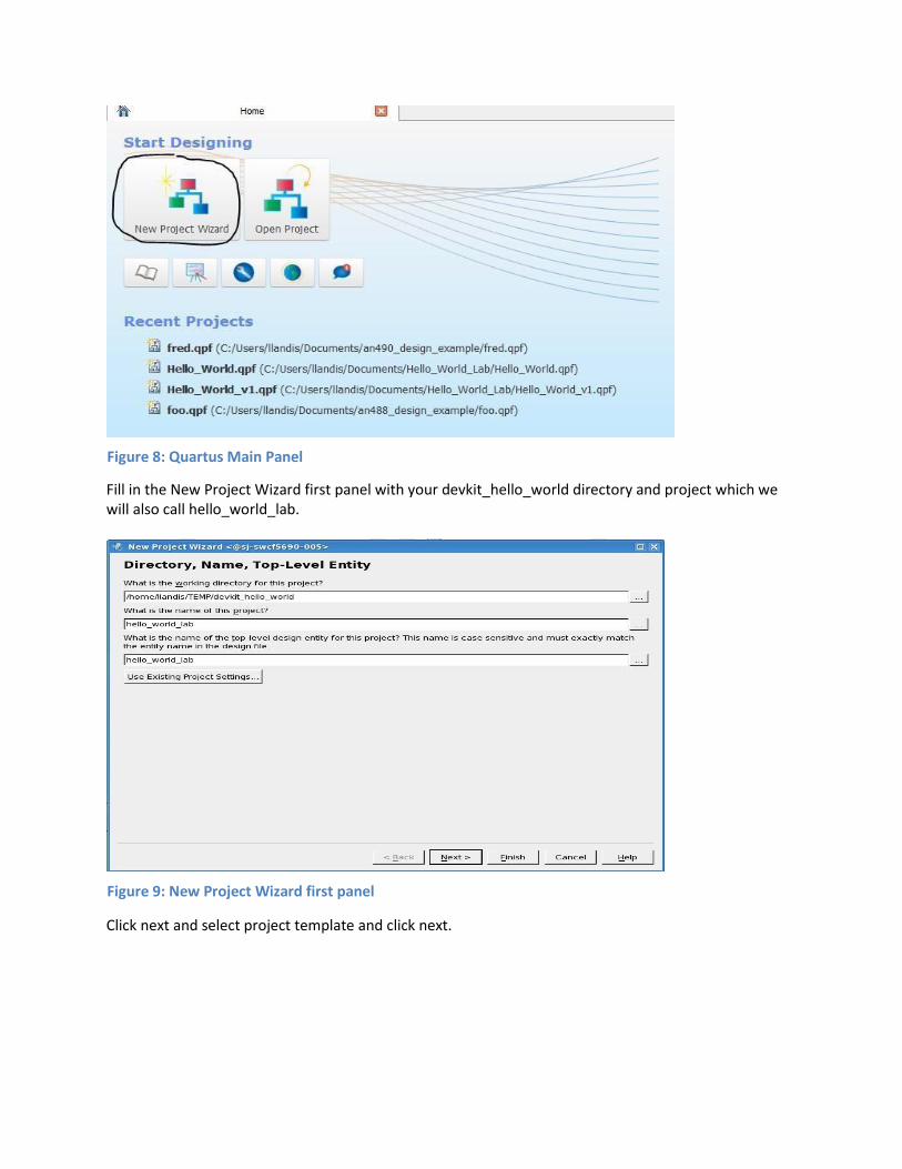
Figure 8: Quartus Main Panel
Fill in the New Project Wizard first panel with your devkit_hello_world directory and project which we will also call hello_world_lab.
Figure 9: New Project Wizard first panel
Click next and select project template and click next.

Figure 10: New project wizard second panel
Figure 11: Design Template Install
Select the DE10_Standard_Golden_Top.par file from your directory into the Design template file(.par) section. Once you hit ok, Quartus loads this starting point design that contains the pinout for the Cyclone V device on the DE10-Standard Development Kit.
Building your Qsys based processor system The Figure 12 diagram illustrates what you are designing in the Qsys environment. This system has a single master, the Nios II processor, and 4 slave devices. Building the Qsys system is a highly efficient way of designing systems with or without a processor. Launch Qsys from Quartus: Tools Qsys. The initial screen looks something like this:

Figure 12: Qsys main panel
Next, we will add the various components of the system and make the connections between them. By default Qsys inserts a clock module. We will connect to this later on in the lab. Below the IP catalog tab, you can search for the various components you want to add to your Qsys based system. Enter Nios in the search tab and select the Nios II Gen 2 processor from the library.
A configuration window will appear, in this select the Nios II/e processor. This version of the Nios II processor is resource optimized and will work well for the Hello World Lab implementation.
Figure 13: Nios II Gen 2 Configuration panel
Click finish and you will see the Nios IIe processor in your connection diagram. For now don’t worry about the system errors reported, we will address them soon.

Figure 14: Qsys System Contents panel
Qsys has a very elegant and efficient way of making connections by clicking on the nodes on ‘wires’ in the connections panel on the 2nd column from the left. You can add the connections as you add components, but it’s often easier to make all the connections once you have finished adding the various blocks. With the Nios II processor added, you still need to add the On Chip Memory, JTAG UART, SWITCHES and LED to your system defined in Figure 4: Nios II based system.
Search for memory in the IP catalog. You will see many options for memory. It might be easiest to detach the IP Catalog from the main panel by clicking on the detach window icon.
Figure 15: Detach window icon
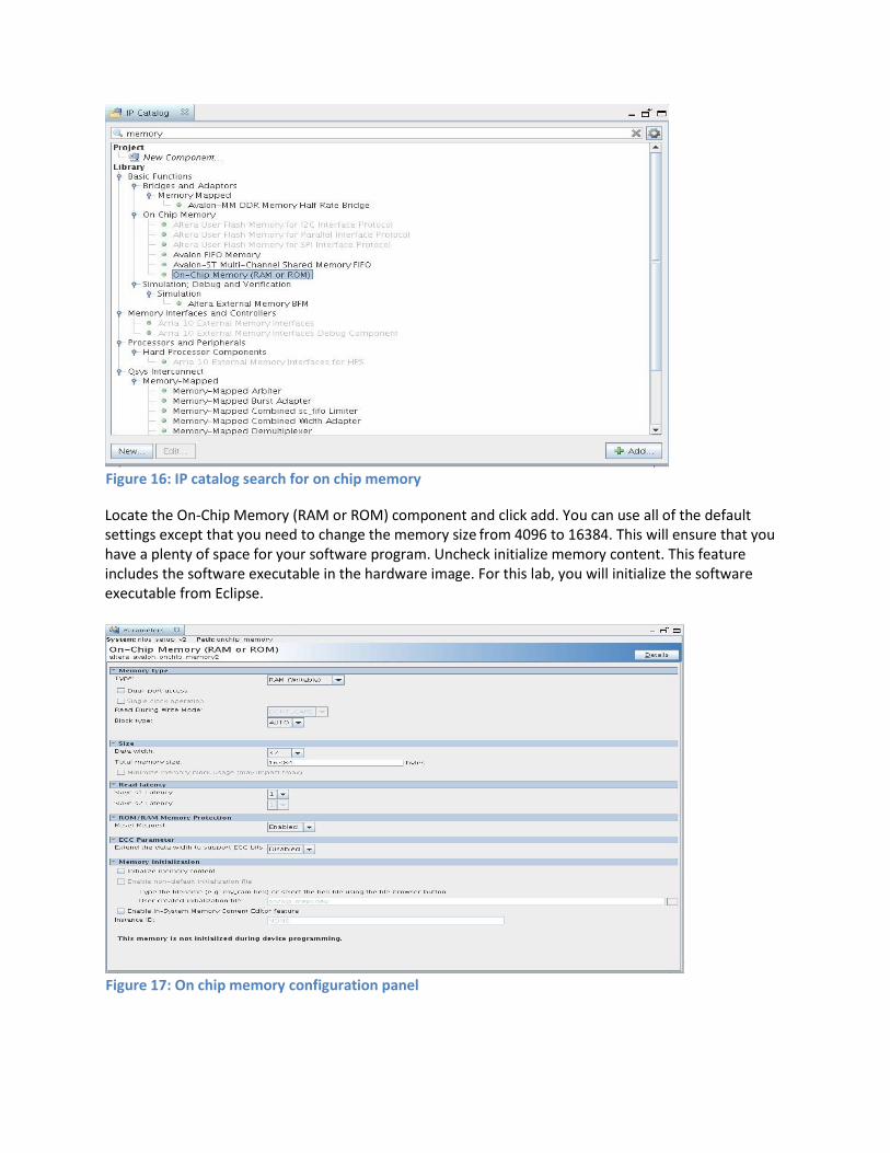
Figure 16: IP catalog search for on chip memory
Locate the On-Chip Memory (RAM or ROM) component and click add. You can use all of the default settings except that you need to change the memory size from 4096 to 16384. This will ensure that you have a plenty of space for your software program. Uncheck initialize memory content. This feature includes the software executable in the hardware image. For this lab, you will initialize the software executable from Eclipse.
Figure 17: On chip memory configuration panel

Click finish and you will now see a total 3 components in your Qsys system: clock, Nios II processor and on-chip memory.
Figure 18: System contents with NIOS-II and on chip memory
The next component you will add is the JTAG UART. Search for JTAG in the IP catalog, locate the JTAG UART and double click or add that component. Keep the default settings and click finish.
Figure 19: JTAG UART configuration panel

The next two components SWITCH and LED are actually configured instances of general purpose parallel IO components in the IP catalog. Search for parallel IO (PIO) and select this block. For the switch block, you will set this up as a 1 bit input interface using the settings shown below.
Figure 20: Parallel IO configuration panel
Next, you will add a second PIO block. Double click on the PIO component as you did for the SWITCH. This time you will configure this component as the LED which is a 1 bit output.
Figure 21: Parallel IO configuration panel for LED outputs

Click finish. You have completed adding the 6 components that make up your Qsys system. Next you will rename the components in the design with names that are easy to remember. In the system contents tab, right click on the nios2_gen_2_0 component, select rename and type in nios2e, similarly rename the rest of the components: onchip_memory, uart, switch and led. This will make these components names easy to remember and reference in future steps.
Figure 22: System Content connections starting panel
The next step consists of making the appropriate connections between the components within Qsys. Click on the clk net coming out of clk_0. When first selected, it will be gray color. Make connections by clicking on on the small open circles on the lines that intersecting with the 5 other components. You should see something similar to Figure 23.
Figure 23: System contents after clock connection

Perform the same operation to connect the clk_reset to the resets on the other components. Next, connect the nios2e data master to the slaves. Make the connections between the Nios2e data master and the s1 connection of the onchip memory, avalon_jtag_slave on the uart, s1 port on the switch and s1 port of the led component as shown below.
Figure 24: System contents after data master/slave connection The instruction master signal from the nios2e component does not need to be connected to each slave component as it only needs access to memory that contains the software executable. Make the connection between the nios2e instruction master and the onchip_memory s1 .

Figure 25: System contents after instruction master/slave connections
The next connections to make are the processor interrupt request (IRQ) signals. The UART can drive interrupts and hence needs to be wired to the nios2e processor interrupt lines. Make this connection as shown in Figure 26. We will use the default setting for the IRQ number.
Figure 26: System contents after interrupt connections
You have now completed the internal connections for this Nios II processor based system. The next step is to make the external connections that connect the Qsys based system to the next higher level in the hierarchy of your FPGA design, or to FPGA device pins that connect to the PCB. Double click on the switch and led conduit items under the export column circled in Figure 27. This will bring these ports out of the Qsys component to connect to the top level design.

Figure 27: System contents after exporting PIO switch and LED
Next you will need to generate the base Addresses for your Qsys system. This is achieved by using the command System -> Assign Base Addresses.
Figure 28: Assign Base addresses
Save your Qsys system by using File Save As and pick a name for the Qsys system that you will remember. Note that the lab figures call it nios_setup_v2 so to avoid confusion you should name your .qsys file the same. The information is saved in what is called a .qsys file. Although you are not entirely finished, it’s good practice to save edits along the way. You should see 2 error messages in the Message Console of Qsys. They are shown in Figure 29.

Figure 29: Error message prior to assign memory location to execute from
These error messages have to do with the fact that nios2e processor doesn’t know where the software code that handles resets and exceptions is located. This is fairly straightforward to fix. Double click on the nios2e component and set the reset vector memory and exception vector memory both to onchip_memory.s1. This will set the system to execute from onchip memory at these respective locations upon reset or interrupt. The 2 errors that were shown in Figure 29 should now be resolved.
Figure 30: Assign vectors in the NIOS2E panel
Save your design once again. Note that by saving, you still have not generated the files that you need for Quartus II compilation or with the Eclipse SBT. The step to complete this is to click on the button on the lower right of Qsys. Click on the button ‘Generate HDL’ and save the file as nios_setup_v2. Click Generate on the panel that appears. Choose Verilog and hit Generate Congratulations, this completes the Qsys section of the lab.

Figure 31: Generating the Qsys system HDL files
Note: If you want to do this project in VHDL, select VHDL option instead of Verilog before generating the HDL as shown in the Figure 31 above.
Building the top level design The next step will take a little bit of knowledge in Verilog. If you want to use a schematic capture editor, jump to appendix A. If you are familiar with VHDL, you can make the same connections in VHDL. During the early steps using the project wizard, you loaded the project template design, and have a preloaded in the Quartus project. We will look at this starting point D10_Standard_Golden_Top.v file and strip out the unnecessary signals, while only leaving the signals that are needed to run the Hello World design. For VHDL you will be able to download the final design file in the upcoming section. Quartus should be open, bring that to the front of your screen. Make sure the hierarchy tab is highlighted and double click the baseline design. Note that for this design there is a clock, reset, push button inputs, LED outputs, and a JTAG UART. The JTAG UART pins are hard wired into the FPGA so you don’t need to add them in your Verilog/VHDL source file. The 4 pins: TCLK, TDI, TMS and TDO that constitute a 4 wire JTAG interface are at a fixed location in your FPGA and they don’t need to be added to your Verilog/VHDL source file. Only pins that are synthesized from your RTL source code need to be specified. The baseline design includes all non hard-wired device pins and you will need to delete extra pins and include the following pins in the port list: CLOCK_50, LEDR, SW. Delete all other pins from the port list. The original DE10_Standard_Golden_Top will have a lot of signals defined and will look like figure 32. Make the changes including changing the module from DE10_Standard_Golden_Top to hello_world and save the file as hello_world.v.

Note - If you want to design in VHDL, change the code into VHDL and save it as hello_world.vhd.
Figure 32: Block diagram of hello_world design
Figure 33: baseline design before editing

Figure 34: Edited baseline design with pins removed. Note save as: hello_world.v
Figure 35 : Edited baseline for VHDL version. Save as hello_world.vhd To download the above code visit:
http://www.alterawiki.com/uploads/b/b9/Hello_world_DE10_Std.v or
http://www.alterawiki.com/uploads/7/7c/Hello_world_DE10_Std.vhd
Next we need to check that the hello_world.v/hello_world.vhd file is included in your project. Note
that it should be the only file in your project so far. Go to Project Add/Remove Files in Project.
Confirm that hello_world.v / hello_world.vhd is listed.

Figure 36: Add/Remove Files pane (for VHDL use hello_world.vhd) Next you need to make the top level entity hello_world. In the same window upper left corner, click on General. Change baseline to hello_world. You can also change by right clicking on the hello_world.v/ hello_world.vhd and set as top level entity.
Figure 37: Settings pane
Click OK when complete. Now it is a good idea to make sure your Verilog/VHDL is syntax correct. Return to the main Quartus window and select the Tasks pane. Double-Click on the Play (right triangle) for

analysis/synthesis. You will get warnings but you should get no errors. If you do get an error, it’s likely syntax (eg missing semicolon). Make changes, save, and continue to run analysis/synthesis until the Verilog/VHDL runs error/free (ignore dangling pin warning for now).
Figure 38: Task pane
The baseline design that you uploaded in the prior steps contain all of the pin settings needed so that the pin locations are consistent with how the DE10-Standard device is connected for the PCB on the DE10-Standard Dev Kit. You can inspect the pin setting locations to understand where they come from. Launch Assignments Assignment Editor. You will see a list of pins in spreadsheet form that contain pin (package ball to be specific) locations, IO standard and current strength settings. Note that you are not using all the pins in the design, but this is ok – Quartus will ignore pin assignments that are not referenced in your design.

Figure 39: Assignment Editor
Adding the Nios II system into your design Now that you have the hello_world entity completed and syntactically correct, you will need to add the Nios II Qsys system into your design. Qsys makes this task quite convenient. Go to File Open and navigate to the name of the Qsys project you created (the one shown in the lab is called nios_setup_v2). You should see a file called nios_setup_v2_inst.v/ nios_setup_v2_inst.vhd . Open this file and you see how to instantiate (fancy word meaning placing this component in your design) the Qsys system. The contents of this file is shown below in Figure 40. You will need to connect the IO ports to the nios_setup_v2. Copy the entire contents of the nios_setup_v2 file by highlighting and copy (ctrl-c), followed by inserting into the Verilog file hello_world.v and pasting (ctrl-v). Next we will connect the push button switches to the LEDs in two different ways to demonstrate how the connection can be made through the FPGA fabric, and in the software that we use that the Nios II executes. To simplify knowing which push button is connected through hardware and which one through software, we will invert the hardware connection so that activating push button 0 turn off LED through a hardware connection, while activating push button 1 turn on the respective LED. Take the push button 0 and connect it to the LED 0 with an inverted assignment (see line 11 in Figure 40). The other LED 1 will be connected through the software.
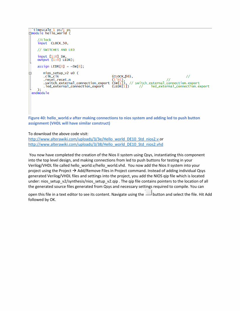
Figure 40: hello_world.v after making connections to nios system and adding led to push button assignment (VHDL will have similar construct) To download the above code visit: http://www.alterawiki.com/uploads/3/3e/Hello_world_DE10_Std_nios2.v or http://www.alterawiki.com/uploads/3/38/Hello_world_DE10_Std_nios2.vhd You now have completed the creation of the Nios II system using Qsys, instantiating this component into the top level design, and making connections from led to push buttons for testing in your Verilog/VHDL file called hello_world.v/hello_world.vhd. You now add the Nios II system into your project using the Project Add/Remove Files in Project command. Instead of adding individual Qsys generated Verilog/VHDL files and settings into the project, you add the NIOS qip file which is located under: nios_setup_v2/synthesis/nios_setup_v2.qip . The qip file contains pointers to the location of all the generated source files generated from Qsys and necessary settings required to compile. You can
open this file in a text editor to see its content. Navigate using the button and select the file. Hit Add followed by OK.

Figure 41: Add/Remove Files from Project - .qip file
Note: Figure shows Verilog, VHDL will be same with .vhd suffix Now you can compile your design which will run analysis & synthesis, fitter (place and route in FPGA terminology), Assembler (generate programming image) and TimeQuest (the static timing analyzer). This can be achieved by clicking on the play button as shown in Figure 42.
Figure 42: Compilation button
Note that some warnings and information messages come up in the bottom window. You can filter by message level. The errors are filtered with the button, critical warnings with the button, warnings with the button and informational messages with the button. You cannot proceed if you have errors. In this case there are only critical and standard warnings, primarily because we did not add timing constraints to this project. Due to the simplicity of this design and low frequency, it’s okay to start without timing constraints. Consult other Altera online training courses for instructions on how to add timing constraints to your design.
Figure 43: Filter for critical warnings
Congratulations, your FPGA hardware design is now complete.

SOFTWARE DESIGN
Creating the Software for the “Hello World” design Should you choose to start directly in the Software Design section and skip the Hardware Design section, consult with your lab facilitator to get these two files: nios_setup_v2.sopcinfo and hello_world_lab.sof as if you generated them from the Hardware Design lab. You will be able to complete all subsequent steps with these two files. The NIOS Software Build Tools for Eclipse are included as part of Quartus. These tools will help manage creation of the application software and Board Support Package (BSP). Launch the SBT Tools NIOS II Software Build Tools for Eclipse. You can use the default location that Eclipse picks for you.
Figure 44: Initial Workspace setup
Click OK in the Workspace launcher. Next, the Eclipse SBT will launch. Right click in the area called Project Explorer and select New Nios II Application and BSP from Template. The BSP is the “Board Support Package” that contains the drivers for things like translating printf C commands to the appropriate instructions to write to the terminal.

Figure 45: Creating the initial project in the Eclipse SBT
Next you will see a panel that requests information to setup your design. First, you need to navigate to your working directory and click on the .sopcinfo file. The .sopcinfo file trains Eclipse on what your Qsys system contains. Click OK.

Figure 46: Navigating to correct .sopcinfo file
Fill in the Project name. Call it hello_world_sw. Next you will be asked to pick a template design. The Hello World Small is a software application to write “Hello from Nios II” to the screen. Click Finish. Note: make sure to pick Hello World Small and not Hello World or you will not have enough memory in your FPGA design to store the program executable.

Figure 47: completing the Nios II Software Examples setup screen with project name and project template. We will now make some modifications to the code to connect the LEDs to the push button switches through software. Click the right arrow next to hello_world_sw. It will show the contents of your project. Double-click hello_world_small.c . Note the command alt_putstr to write text to the terminal. This is part of the Altera HAL (Hardware Abstraction Layer) set of software functions. A complete list of these functions can be found in the Nios II Software Developer’s Handbook https://www.altera.com/en_US/pdfs/literature/hb/nios2/n2sw_nii5v2.pdf .

Figure 48: hello_world_small.c
Next you need to add a library declaration, define integer switch_datain, and a few HAL functions to connect the LEDs to the Push Buttons: #include <sys/alt_stdio.h> #include <stdio.h> #include "altera_avalon_pio_regs.h" #include "system.h" int main() { int switch_datain; alt_putstr("Hello from Nios II!\n"); /* Event loop never exits. Read the PB, display on the LED */ while (1){ switch_datain = IORD_ALTERA_AVALON_PIO_DATA(SWITCH_BASE); IOWR_ALTERA_AVALON_PIO_DATA(LED_BASE,switch_datain); } return 0; } Note the use of the variables SWITCH_BASE and LED_BASE. These variables are created by importing the information from the .sopcinfo file. You can find defined variables in the system.h file under the hello_world_sw_bsp project. Double click on system.h file and inspect the defined variable names for SWITCH_BASE and LED_BASE. These must match your hello_world_small.c code. Edit
the hello_world_small.c source code so that it matches the code shown above. Click the save icon. Right click on the hello_world_sw project. Left click Build. This compiles the software application and the BSP (drivers).

Figure 49: Launching the build
Once the build completes, you should observe a “.elf” file (executable load file) under the hello_world_sw project. If the .elf file does not exist, the project did not build properly. Inspect the problems tab on the bottom of the Eclipse SBT and determine if there are syntax problems, correct, and rerun Build Project. Typical problems can be missing semicolons, mismatched brackets and such.
Figure 50: The presence of hello_world_sw.elf indicates the
software build ran successfully

Downloading the hardware image to the DE10-Standard Development Kit To work with the DE10-Standard development kit in the context of this lab, you will need to connect the power supply to the DC Input and a USB cable connecting the kit to a host PC. It is very important to note that there are 2 USB connectors: USB Blaster and USB UART. You must connect the USB cable to the USB Blaster. The USB blaster utilizes circuitry that formats the image into a data stream that downloads from the PC to FPGA. If you connect to the USB UART connector, your image will fail to download.
Make sure your development kit is powered up and LEDs are on.
Figure 51: USB Cable and Power source connected
If you are only performing the Software design lab, you must first launch Quartus. If you have just performed the Hardware Design lab, then Quartus should already be open. Launch the Programmer: Tools Programmer. Click Auto Detect and you should see something similar to Figure 52.

Figure 52: Programmer after Auto Detect
Next, you need to download what is called a “.sof” file or SRAM object file. This is the programming image file that gets downloaded in the FPGA. The default location is <working_directory>/output_files. Right click on the first row <none> under File and click on Change File. Navigate to the output_files directory and select hello_world_lab.sof. Click Open. In the first row under Program/Configure click in the check box as shown in Figure 52. Click Start. When programming is complete, the Progress
meter should read 100% (Successful).
Figure 53: Programmer after completing .sof download

Now it is time to download the .elf (software executable) into the Nios IIe processor. Return to the Eclipse SBT tools. Right click on hello_world_sw and select Run as Run Nios II Hardware. Click on the Target Connection tab. The connection should indicate that Eclipse has connected to USB-blaster. If the connection is not identified, you can Click Refresh Connections. Note that you might need to stretch the window wider to see the Refresh Connections button. Once the connection is made to the USB-Blaster, you should observe something similar to Figure 54. Click Run.
Figure 54: Run (Nios II) Configurations Window in Eclipse.
Now you have hardware and software downloaded into your Kit. Development Kit. You should observe “Hello from Nios II” in the Nios II Console tab.
Figure 55: “Hello from Nios II!” displayed on the Nios II Console

You can also test the connections between push button and LEDs. Recall that switch 0 is connected in hardware is inverted so by default the LED is on. Switch 1 is connected in the C code and illuminate LED 1 when pushed. Refer to the diagram below and confirm that the switches operate the LEDs based on the hello_world.v and hello_world.c source files.
Figure 56: Operating the hello_world lab.
Lab Summary You now have completed the hardware and software sections of this lab. This includes:
1. Loading the Device Kit pin settings into Quartus 2. Using Qsys to build a Nios II based system 3. Instantiating the Qsys component into your top level design 4. Add some connections between push buttons and LEDs 5. Compiling your hardware 6. Importing the Nios II based system into the Eclipse Software Build Tools 7. Building a software project 8. Modifying a software template to perform some simple IO functions 9. Compiling your software 10. Downloading the hardware image into the DE10-Standard Development Kit 11. Downloading the software executable into the DE10-Standard Development Kit 12. Testing the hardware
There is a wealth of resources from Altera and partners to take classes on Embedded Hardware, Embedded Software and reference design starting points to advance your skills using Altera’s powerful Nios II based hardware and software tools.

Appendix A: Using Schematic Capture in place of writing Verilog/VHDL for the top level module
In the section, Building the Top Level Design, we showed you how to create the top level design that instantiates the Nios II Qsys system by typing in the Verilog description of the connections. An alternative means to make these connections is by using the schematic capture tool within Quartus. The two means to create the top design: Verilog edits, and schematic capture are generally a matter of preference and familiarity with the Verilog language. The industry trends toward editing Verilog or VHDL hardware description languages, but either means will generate a working FPGA design. Launch the schematic capture tool by invoking File New Block Diagram/Schematic File You will see a blank schematic as shown in Figure 57.
Figure 57: Blank schematic page
Next you will need to add the Qsys system block. Right click and invoke insert symbol. Under name, navigate to working directory/nios_setup_v2 and select nios_setup.bsf. Click Open. Then click OK.

Figure 58: Adding the nios_setup_v2 symbol into your schematic Click in the middle of the screen and drop the symbol in the middle of the screen with a left click. Right click again in an empty area of the schematic. This time you will be adding the inversion between the SW[1] and LEDR[1]. Click Insert symbol. Navigate to primitives logic NOT and highlight. Click OK. Drop the NOT symbol below the nios_setup_v2 symbol.
Figure 59: After adding the nios_setup_v2 and NOT symbols into your schematic
Now you need to make the connections to the schematic. Locate the pin icon and select input. Snap the input to clock, reset and switch on the nios_setup_v2 and to the input of the NOT. Hit escape. Select the output pin and snap to the output of NOT and drop another one to the left of the nios_setup_v2 symbol without connecting it since its pointing in the wrong direction. Hit escape. Right click the output pin near the nios_setup_v2 and Flip Horizontal. Left click the output pin and snap it to the led_external_connection_export port on nios_setup_v2.

Now you need to determine the appropriate names for the pin connections. Open the assignment editor as shown in Figure 38. Locate the names of the signals for reference: CLOCK_50, SW, LEDR. Right click on the pins in your schematic and invoke properties and change the pin names to the appropriate top level ports. Make sure the names are identical to the assignment editor. Note that bus notation is of the form SW[1]. The nios_setup_v2 gets pin [0] and the NOT gets pins [1]. Once you have assigned the port names, you have completed the schematic. Click save as and enter hello_world.bdf. The completed schematic is shown in Figure 60.
Figure 60: Completed schematic with pin connections
Now you need to add the hello_world.bdf to your project by clicking Project Add/Remove Files in Project. Add the hello_world.bdf file if not already there. Now you are ready to return to the compilation step in Figure 41. Continue the subsequent steps through the hardware and software development sections.
Appendix B: Merging the NIOS executable into the FPGA configuration file (Hardware Image) In this section, we will guide you with “how to merge the software executable file (Nios II .elf file) into hardware image (.sof file)”. The master_image directory shipped with the design example .sof and .pof files have the NIOS executable incorporated in them. The prior steps detailing how to build your hardware and software show you how to compile the hardware without the image loaded in the .sof or .pof file. In those steps, you load the NIOS executable from Eclipse through the Run > NIOSII Hardware step. This section will allow you to merge the .elf executable into the .sof once your software is stable. In Eclipse, right click on the project and select Make Target > Build, a window pops up, then select mem_init_generate > Build. This generates a .hex file that is in the location where your software build is located (e.g): ./Hello_World_Dev_kit/software/hello_world_sw/mem_init/nios_setup_v2_on chip_memory.hex

Figure 61:Selecting mem_init_generate
Next, you need to return to Qsys and change the onchip_memory component by double clicking it. Check all the boxes in “Memory Initialization” and enter the location of .hex file where it is located in “User created initialization file”.
Figure 62: Initializing onchip_memory component Next, click Generate HDL > Generate. Return to Quartus and click compile and you will generate a new .sof file with the NIOS executable included. Run the programmer and download the new .sof. Run the demonstration as described in the previous steps.

Appendix C: Using Interrupt Service Routines (ISR) in a NIOS based system
Theory of Operation The hello_world.c demonstration uses a polling technique to monitor the values of the push buttons. An infinite while(1) loop is used and each time through the loop the value of the push buttons are monitored. Another means to monitor events is through the use of interrupts. The theory of operation of how hardware interrupts work is shown in Figure 62. The appendix explains how to implement hardware implements using NIOSII and hardware abstraction layer (HAL) functions.
Figure 63: Interrupt architecture
Interrupts gain priority over any code such as while loops, for loops etc. which are executing. This section demonstrates how software registers an Interrupt Service Routine (ISR) using the alt_ic_isr_register() HAL function. The hardware abstraction layer (HAL) registers the ISR by configuring the vector table. The return code from alt_ic_isr_register() is zero if the function succeeds, and nonzero if it fails. If the HAL registers an ISR successfully, the associated Nios II hardware interrupt (as defined by irq) is enabled on return from alt_ic_isr_register().The main components of this HAL function are as follows:
1. SWITCH_IRQ_INTERRUPT_CONTROLLER_ID – Interrupt controller ID (refer to system.h) 2. SWITCH_IRQ – IRQ number (refer to system.h) 3. handle_button_interrupts(ISR) – Pointer to ISR function 4. edge_capture_ptr – Argument passed to the ISR 5. 0x0 – Flag (reserved)
The ISR reads the value of the push buttons and updates the pointer to the variable edge_capture. The pointer edge_capture_ptr reads the new value on the push buttons. For more details about

alt_ic_isr_register() and its parameters, please refer Exception Handling, NIOS || Software Developer's Handbook - Altera.
Steps to compile the interrupt enabled software • The C program with the hardware interrupts used is present in the hello_world_interrupt.c file
in the software folder.
• Copy the contents of the file into the hello_world.c file, or replace hello_world.c with hello_world_interrupt.c
• Program the board with the .sof file as explained in Downloading the hardware image to the DE10-Standard Development Kit.
• Build the design and run it on the hardware.
Demonstration to explain the execution of the design
a: Blink continuously with hardware interrupts
The main menu gives the user an option to select between the modes of operation. The menu is displayed by calling the functions TopMenu, MenuBegin and MenuEnd. The input from the user is read using the function GetInputString. The console displays it as: To start the blinking process the user needs to press PB2. The console displays the following message:In the blink continuous mode the LED2 blinks continuously until the user interrupts it by pressing PB3. When there is an interrupt, the following message is displayed:
If the user wishes to continue blinking they have to press PB2 again or if they wish to exit out of the loop they have to press PB3.
b: Blink number of times entered by user In this mode of operation the GetInputString() function reads a number in the range 0 to 9 entered by the user. The LED2 and LED3 blink for the number of times specified by the user and exits the loop. The image below shows the messages the user must observe in this mode:

Thank you!