Embed Size (px)
Citation preview

MMG3005NT1
1RF Device DataFreescale Semiconductor
MMG3005NT1
Heterojunction Bipolar TransistorTechnology (InGaP HBT)Broadband High Linearity AmplifierThe MMG3005NT1 is a general purpose amplifier that is internally
prematched and designed for a broad range of Class A, small--signal, highlinearity, general purpose applications. It is suitable for applications withfrequencies from 800 to 2200 MHz such as cellular, PCS, WLL, PHS,VHF, UHF, UMTS and general small--signal RF.
Features Frequency: 800--2200 MHz P1dB: 30 dBm @ 2140 MHz Small--Signal Gain: 15 dB @ 2140 MHz Third Order Output Intercept Point: 47 dBm @ 2140 MHz Single 5 V Supply Internally Prematched to 50 Ohms In Tape and Reel. T1 Suffix = 1,000 Units, 16 mm Tape Width, 13--inch Reel.
800--2200 MHz, 15 dB30 dBm
InGaP HBT GPA
PQFN 5 5
Table 1. Typical Performance (1)
Characteristic Symbol900MHz
1960MHz
2140MHz Unit
Small--Signal Gain(S21)
Gp 18.5 15.5 15 dB
Input Return Loss(S11)
IRL --14 --10 --11 dB
Output Return Loss(S22)
ORL --12 --7 --7 dB
Power Output @1dBCompression
P1db 30 30 30 dBm
Third Order OutputIntercept Point
OIP3 47 47 47 dBm
1. VDC = 5 Vdc, TA = 25C, 50 ohm system, application circuittuned for specified frequency.
Table 2. Maximum Ratings
Rating Symbol Value Unit
Supply Voltage VDC 6 V
Supply Current IDC 600 mA
RF Input Power Pin 18 dBm
Storage Temperature Range Tstg --65 to +150 C
Junction Temperature TJ 150 C
Table 3. Thermal Characteristics
Characteristic Symbol Value (2) Unit
Thermal Resistance, Junction to CaseCase Temperature 100C, 5 Vdc, 480 mA, no RF applied
RJC 21.5 C/W
2. Refer to AN1955, Thermal Measurement Methodology of RF Power Amplifiers. Go to http://www.freescale.com/rf.Select Documentation/Application Notes -- AN1955.
Document Number: MMG3005NT1Rev. 9, 10/2014
Freescale SemiconductorTechnical Data
Freescale Semiconductor, Inc., 2005--2011, 2014. All rights reserved.

2RF Device Data
Freescale Semiconductor
MMG3005NT1
Table 4. Electrical Characteristics (VDC = 5 Vdc, 2140 MHz, TA = 25C, 50 ohm system, in Freescale Application Circuit)
Characteristic Symbol Min Typ Max Unit
Small--Signal Gain (S21) Gp 14 15 — dB
Input Return Loss (S11) IRL — --11 — dB
Output Return Loss (S22) ORL — --7 — dB
Power Output @ 1dB Compression P1dB — 30 — dBm
Third Order Output Intercept Point OIP3 — 47 — dBm
Noise Figure NF — 5 — dB
Supply Current IDC 420 480 520 mA
Supply Voltage VDC — 5 — V
Table 5. Functional Pin Description
NamePin
Number Description
RFin 3, 4 RF input for the power amplifier. This pin is DC--coupled andrequires a DC--blocking series capacitor.
RFout/VCC
10, 11, 12 RF output for the power amplifier. This pin is DC--coupledand requires a DC--blocking series capacitor.
VCC 14 Collector voltage supply.
VBA 16 Bias voltage supply.
GND BacksideCenterMetal
The center metal base of the PQFN package provides bothDC and RF ground as well as heat sink contact for thepower amplifier.
Table 6. ESD Protection Characteristics
Test Methodology Class
Human Body Model (per JESD 22--A114) 1A
Machine Model (per EIA/JESD 22--A115) A
Charge Device Model (per JESD 22--C101) IV
Table 7. Moisture Sensitivity Level
Test Methodology Rating Package Peak Temperature Unit
Per JESD 22--A113, IPC/JEDEC J--STD--020 3 260 C
RFout/VCC
RFout/VCC
Figure 1. Pin Connections
(Top View)
1
VBA VCC
RFout/VCC
RFin
RFin
13
5 9
2 12
3 11
4 10
16 15 14
6 7 8
N.C.
N.C.N.C.
N.C.N.C. N.C.
N.C.N.C.
N.C.

MMG3005NT1
3RF Device DataFreescale Semiconductor
50 OHM TYPICAL CHARACTERISTICS
I CC,COLLECTORCURRENT(mA)
0
600
0
VBA, BIAS VOLTAGE (V)
Figure 2. Collector Current versus Bias Voltageat Pin 16
360
240
1 2 3 5
VCC = 5 Vdc
480
120
4
305 10 15 20 2520
55
Pout, OUTPUT POWER (dBm)
Figure 3. Third Order Output Intercept Pointversus Output Power and Supply Current
45
40
35
30
IP3,THIRDORDER
OUTPUTINTERCEPTPOINT(dBm
)
25
50
VDC = 5 Vdcf1 = 2140 MHzf2 = 2141 MHz
IDC = 480 mA400 mA
320 mA
NOTE: Supply current is varied under external resistor control. Peak poweris not reducedat any listed current. Similar results canbeobtained for otherfrequency bands.
150103
106
120
Figure 4. MTTF versus Junction Temperature
104
125 130 135 140 145
TJ, JUNCTION TEMPERATURE (C)
NOTE: The MTTF is calculated with VDC = 5 Vdc, IDC = 480 mA
MTTF(YEARS) 105
Pin Connections
RFout/VCC
RFout/VCC
(Top View)
1
VBA VCC
RFout/VCC
RFin
RFin
13
5 9
2 12
3 11
4 10
16 15 14
6 7 8
N.C.
N.C.N.C.
N.C.N.C. N.C.
N.C.N.C.
N.C.

4RF Device Data
Freescale Semiconductor
MMG3005NT1
50 OHM APPLICATION CIRCUIT: 900 MHz
Figure 5. 50 Ohm Test Circuit Schematic
Z1, Z7 0.140 x 0.028 MicrostripZ2, Z6 0.057 x 0.028 MicrostripZ3 0.342 x 0.028 Microstrip
Z4 0.119 x 0.028 MicrostripZ5 0.223 x 0.028 MicrostripPCB Isola FR408, 0.014, r = 3.7
RFOUTPUT
RFINPUT
R1
L1
C7C1
Z1 Z2 Z3
C4C3
R2
VSUPPLY
16
DUT C8
Z4 Z5 Z6
C2
Z7
C6C5
Current Mirror
15 14
6 7 8
1 13
5 9
2
3
4
12
11
10
Table 8. 50 Ohm Test Circuit Component Designations and ValuesPart Description Part Number Manufacturer
C1, C2 15 pF Chip Capacitors ECUV1H150JCV Panasonic
C3, C5 0.01 F Chip Capacitors C0603C103J5RAC Kemet
C4, C6 0.1 F Chip Capacitors C0603C104J5RAC Kemet
C7 6.8 pF Chip Capacitor 06035J6R8BS AVX
C8 5.6 pF Chip Capacitor 06035J5R6BS AVX
L1 15 nH Chip Inductor 1008CS--150XJB Coilcraft
R1 33 Ω, 1/10 W Chip Resistor CRCW060333R0FKEA Vishay
R2 0 Ω, 1/10 W Chip Resistor CRCW06030000FKEA Vishay

MMG3005NT1
5RF Device DataFreescale Semiconductor
50 OHM APPLICATION CIRCUIT: 900 MHz
C4
C3
R2
C6
C5
L1
C8C2C7C1
MMG3004/5 Rev 3
Figure 6. 50 Ohm Test Circuit Component Layout
R1
RFin RFout
VSUPPLYVBA

6RF Device Data
Freescale Semiconductor
MMG3005NT1
50 OHM TYPICAL CHARACTERISTICS: 900 MHz
15
20
840
f, FREQUENCY (MHz)
Figure 7. Small--Signal Gain (S21) versusFrequency
VDC = 5 Vdc
18
16Gp,SM
ALL--SIGNAL
GAIN(dB) TC = --40C19
17
870 900 930 960
25C85C
--15
--10
f, FREQUENCY (MHz)
Figure 8. Input Return Loss (S11) versusFrequency
--14IRL,INPUTRETURNLOSS
(dB)
--12
--11
--13
VDC = 5 Vdc
TC = --40C25C
85C
840 870 900 930 960
--15
--5
f, FREQUENCY (MHz)
Figure 9. Output Return Loss (S22) versusFrequency
--13
ORL,OUTPUTRETURNLOSS
(dB)
--9
--7
--11
VDC = 5 Vdc
TC = --40C
25C
85C
840 870 900 930 96028
32
30
29
f, FREQUENCY (MHz)
Figure 10. P1dB versus Frequency
P1dB,1dB
COMPRESSIONPOINT(dBm
)
31
840 870 900 930 960
VDC = 5 Vdc
TC = --40C
25C85C
40
50
48
46
44
42
840 870 900 930 960
f, FREQUENCY (MHz)
Figure 11. Third Order Output InterceptPoint versus Frequency
IP3,THIRDORDER
OUTPUTINTERCEPTPOINT(dBm
)
VDC = 5 Vdc1 MHz Tone Spacing
TC = --40C
25C
85C
0
10
f, FREQUENCY (MHz)
Figure 12. Noise Figure versus Frequency
6
4
2
NF,NOISEFIGURE(dB)
840 870 900 930 960
VDC = 5 Vdc
TC = 85C
25C
--40C
8

MMG3005NT1
7RF Device DataFreescale Semiconductor
50 OHM TYPICAL CHARACTERISTICS: 900 MHz
29
--55
--35
24
Pout, OUTPUT POWER (dBm)
Figure 13. IS--95 Adjacent Channel Power Ratioversus Output Power
--40
--45
--50
28272625
ACPR,ADJACENTCHANNEL
POWER
RATIO(dBc)
TC = --40C25C
85C
29
--80
--40
19
Pout, OUTPUT POWER (dBm)
Figure 14. IS--95 Adjacent Channel Power Ratioversus Output Power
--50
--60
--70
27252321
ACPR,ADJACENTCHANNEL
POWER
RATIO(dBc)
TC = 85C
25C
--40C
VDC = 5 Vdc, f = 900 MHzSingle--Carrier IS--95, 9 Channel Forward750 kHz Measurement Offset30 kHz Measurement Bandwidth
VDC = 5 Vdc, f = 900 MHzSingle--Carrier IS--95, 9 Channel Forward885 kHz Measurement Offset30 kHz Measurement Bandwidth

8RF Device Data
Freescale Semiconductor
MMG3005NT1
50 OHM APPLICATION CIRCUIT: 1800--2200 MHz
Figure 15. 50 Ohm Test Circuit Schematic
Z1, Z7 0.140 x 0.028 MicrostripZ2 0.269 x 0.028 MicrostripZ3 0.130 x 0.028 MicrostripZ4 0.044 x 0.028 Microstrip
Z5 0.075 x 0.028 MicrostripZ6 0.280 x 0.028 MicrostripPCB Isola FR408, 0.014, r = 3.7
RFOUTPUT
RFINPUT
R1
L1
C7C1
Z1 Z2 Z3
C4C3
R2
VSUPPLY
16
DUT C8
Z4 Z5 Z6
C2
Z7
C6C5
Current Mirror
15 14
6 7 8
1 13
5 9
2
3
4
12
11
10
Table 9. 50 Ohm Test Circuit Component Designations and ValuesPart Description Part Number Manufacturer
C1 15 pF Chip Capacitor ECUV1H150JCV Panasonic
C2 1.8 pF Chip Capacitor 06035J1R8BS AVX
C3, C5 0.01 F Chip Capacitors C0603C103J5RAC Kemet
C4, C6 0.1 F Chip Capacitors C0603C104J5RAC Kemet
C7 2.7 pF Chip Capacitor 06035J2R7BS AVX
C8 1.2 pF Chip Capacitor 06035J1R2BS AVX
L1 15 nH Chip Inductor 1008CS--150XJB Coilcraft
R1 33 Ω, 1/10 W Chip Resistor CRCW060333R0FKEA Vishay
R2 0 Ω, 1/10 W Chip Resistor CRCW06030000FKEA Vishay

MMG3005NT1
9RF Device DataFreescale Semiconductor
50 OHM APPLICATION CIRCUIT: 1800--2200 MHz
Figure 16. 50 Ohm Test Circuit Component Layout
C4
C3
R2
C6
C5
L1
C8 C2C7C1
MMG3004/5 Rev 3
R1
RFin RFout
VSUPPLYVBA

10RF Device Data
Freescale Semiconductor
MMG3005NT1
50 OHM TYPICAL CHARACTERISTICS: 1800--2200 MHz
12
18
1900
f, FREQUENCY (MHz)
Figure 17. Small--Signal Gain (S21) versusFrequency
VDC = 5 Vdc
16
13
Gp,SM
ALL--SIGNAL
GAIN(dB)
TC = --40C
17
15
25C85C14
1960 2020 2080 2140 2200
--20
--5
f, FREQUENCY (MHz)
Figure 18. Input Return Loss (S11) versusFrequency
--15
IRL,INPUTRETURNLOSS
(dB)
--10
VDC = 5 Vdc
TC = --40C
25C85C
1900 1960 2020 2080 2140 2200
--10
0
f, FREQUENCY (MHz)
Figure 19. Output Return Loss (S22) versusFrequency
--8
ORL,OUTPUTRETURNLOSS
(dB)
--4
--2
--6
VDC = 5 Vdc
TC = --40C
25C85C
1900 1960 2020 2080 2140 220028
32
30
29
f, FREQUENCY (MHz)
Figure 20. P1dB versus Frequency
P1dB,1dB
COMPRESSIONPOINT(dBm
)
31
VDC = 5 Vdc
TC = --40C
25C
85C
1900 1960 2020 2080 2140 2200
40
50
48
46
44
42
f, FREQUENCY (MHz)
Figure 21. Third Order Output InterceptPoint versus Frequency
IP3,THIRDORDER
OUTPUTINTERCEPTPOINT(dBm
)
VDC = 5 Vdc1 MHz Tone Spacing
TC = --40C
25C
85C
0
10
f, FREQUENCY (MHz)
Figure 22. Noise Figure versus Frequency
6
4
2
NF,NOISEFIGURE(dB)
VDC = 5 Vdc
TC = 85C
25C--40C
8
1900 1960 2020 2080 2140 2200 1900 1960 2020 2080 2140 2200

MMG3005NT1
11RF Device DataFreescale Semiconductor
50 OHM TYPICAL CHARACTERISTICS: 1800--2200 MHz
29
--55
--35
24
Pout, OUTPUT POWER (dBm)
Figure 23. IS--95 Adjacent Channel Power Ratioversus Output Power
--40
--45
--50
28272625
ACPR,ADJACENTCHANNEL
POWER
RATIO(dBc)
TC = 85C25C
--40C
29
--80
--40
19
Pout, OUTPUT POWER (dBm)
Figure 24. IS--95 Adjacent Channel Power Ratioversus Output Power
--50
--60
--70
27252321
ACPR,ADJACENTCHANNEL
POWER
RATIO(dBc)
TC = 85C
25C--40C
28
--70
--20
18
Pout, OUTPUT POWER (dBm)
Figure 25. Single--Carrier W--CDMA AdjacentChannel Power Ratio versus Output Power
--30
--40
--50
--60
26242220
VDC = 5 Vdc, f = 2140 MHzSingle--Carrier W--CDMA, 3.84 MHz Channel BandwidthInput Signal PAR = 8.5 dB @ 0.01% Probability (CCDF)
ACPR,ADJACENTCHANNEL
POWER
RATIO(dBc)
TC = 85C25C
--40C
VDC = 5 Vdc, f = 1960 MHzSingle--Carrier IS--95, 9 Channel Forward750 kHz Measurement Offset30 kHz Measurement Bandwidth
VDC = 5 Vdc, f = 1960 MHzSingle--Carrier IS--95, 9 Channel Forward885 kHz Measurement Offset30 kHz Measurement Bandwidth

12RF Device Data
Freescale Semiconductor
MMG3005NT1
50 OHM TYPICAL CHARACTERISTICS
Table 10. Common Emitter S--Parameters (VDC = 5 Vdc, TA = 25C, 50 Ohm System)
fMHz
S11 S21 S12 S22
|S11| |S21| |S12| |S22|
250 0.70575 --173.81 5.06022 143.91 0.00976 --49.75 0.84913 174.65
300 0.73140 --174.91 4.79122 137.40 0.00866 --46.60 0.84273 173.16
350 0.75442 --176.26 4.52885 131.51 0.00773 --43.76 0.83759 172.12
400 0.77553 --177.67 4.27831 126.11 0.00689 --40.58 0.83409 171.28
450 0.79364 --179.04 4.03762 121.18 0.00618 --36.61 0.83042 170.63
500 0.80933 179.58 3.82617 116.75 0.00565 --31.68 0.83214 170.43
550 0.82301 178.27 3.62033 112.46 0.00523 --26.34 0.83079 169.99
600 0.83429 177.07 3.43310 108.55 0.00494 --20.59 0.82956 169.83
650 0.84357 175.98 3.26377 104.82 0.00478 --15.13 0.82812 169.78
700 0.85132 174.99 3.10735 101.29 0.00468 --10.28 0.82590 169.86
750 0.85696 174.16 2.96322 97.96 0.00459 --5.76 0.82489 170.15
800 0.86176 173.35 2.82568 94.86 0.00454 --1.51 0.82589 170.57
850 0.86572 172.60 2.70160 92.31 0.00452 3.52 0.82783 171.07
900 0.86813 171.85 2.60468 90.11 0.00455 7.99 0.83010 171.50
950 0.86945 171.15 2.53732 88.04 0.00475 12.64 0.83192 172.00
1000 0.86974 170.42 2.48944 85.86 0.00498 15.23 0.83202 172.45
1050 0.86842 169.66 2.45821 83.61 0.00517 16.96 0.83128 172.96
1100 0.86533 168.91 2.44429 81.27 0.00537 18.37 0.82923 173.50
1150 0.86095 168.14 2.44811 78.81 0.00562 19.48 0.82679 174.01
1200 0.85480 167.25 2.46595 76.18 0.00589 19.73 0.82313 174.63
1250 0.84684 166.25 2.49650 73.39 0.00614 19.47 0.81800 175.29
1300 0.83707 165.18 2.54318 70.39 0.00639 18.66 0.81154 176.08
1350 0.82469 164.00 2.60413 67.17 0.00664 17.14 0.80396 176.98
1400 0.80971 162.76 2.68767 63.69 0.00686 15.10 0.79812 177.98
1450 0.79087 161.42 2.79189 59.73 0.00707 12.45 0.79179 178.83
1500 0.76847 160.03 2.91082 55.24 0.00723 8.99 0.78258 179.68
1550 0.74126 158.60 3.04944 50.25 0.00735 4.62 0.77256 --179.28
1600 0.70933 157.30 3.20126 44.67 0.00737 --0.89 0.76200 --178.18
1650 0.67261 156.25 3.36356 38.42 0.00727 --7.59 0.75243 --176.93
1700 0.63202 155.73 3.53052 31.45 0.00702 --15.85 0.74435 --175.63
1750 0.59058 156.13 3.69596 23.72 0.00657 --25.99 0.73950 --174.33
1800 0.55219 157.76 3.84647 15.21 0.00592 --38.78 0.73766 --173.25
1850 0.53906 175.46 3.84639 5.98 0.00493 --55.47 0.74863 173.64
1900 0.55077 --178.72 3.76728 --3.57 0.00394 --78.20 0.76239 172.14
1950 0.58350 --174.08 3.61364 --13.31 0.00325 --110.26 0.77658 170.13
2000 0.63044 --171.29 3.40538 --22.98 0.00325 --147.37 0.78891 167.72
2050 0.68283 --170.32 3.15278 --32.28 0.00389 --177.72 0.79795 164.96
2100 0.73327 --170.78 2.87824 --41.07 0.00480 161.34 0.80422 162.03
2150 0.77875 --172.14 2.60183 --49.24 0.00576 146.52 0.80618 159.04
2200 0.81666 --174.06 2.33461 --56.78 0.00658 135.49 0.80601 156.02
2250 0.84807 --176.25 2.08577 --63.69 0.00728 126.95 0.80299 153.08
2300 0.87279 --178.55 1.85911 --70.01 0.00782 120.20 0.79865 150.21
2350 0.89261 179.07 1.65704 --75.82 0.00823 114.85 0.79341 147.45
2400 0.90758 176.70 1.47812 --81.19 0.00851 110.74 0.78715 144.80
2450 0.91984 174.31 1.32091 --86.22 0.00868 107.68 0.78067 142.25
(continued)
MMG3005NT1
13RF Device DataFreescale Semiconductor
50 OHM TYPICAL CHARACTERISTICS
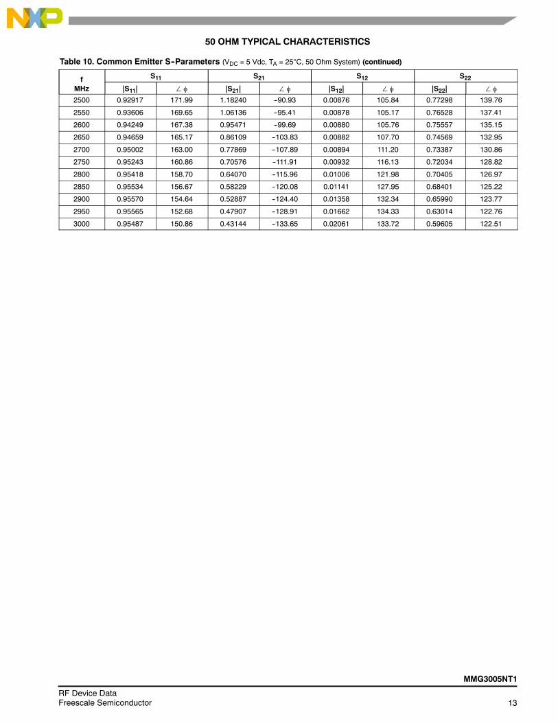
Table 10. Common Emitter S--Parameters (VDC = 5 Vdc, TA = 25C, 50 Ohm System) (continued)
fMHz
S11 S21 S12 S22
|S11| |S21| |S12| |S22|
2500 0.92917 171.99 1.18240 --90.93 0.00876 105.84 0.77298 139.76
2550 0.93606 169.65 1.06136 --95.41 0.00878 105.17 0.76528 137.41
2600 0.94249 167.38 0.95471 --99.69 0.00880 105.76 0.75557 135.15
2650 0.94659 165.17 0.86109 --103.83 0.00882 107.70 0.74569 132.95
2700 0.95002 163.00 0.77869 --107.89 0.00894 111.20 0.73387 130.86
2750 0.95243 160.86 0.70576 --111.91 0.00932 116.13 0.72034 128.82
2800 0.95418 158.70 0.64070 --115.96 0.01006 121.98 0.70405 126.97
2850 0.95534 156.67 0.58229 --120.08 0.01141 127.95 0.68401 125.22
2900 0.95570 154.64 0.52887 --124.40 0.01358 132.34 0.65990 123.77
2950 0.95565 152.68 0.47907 --128.91 0.01662 134.33 0.63014 122.76
3000 0.95487 150.86 0.43144 --133.65 0.02061 133.72 0.59605 122.51

14RF Device Data
Freescale Semiconductor
MMG3005NT1
Figure 26. Recommended Mounting Configuration
NOTES:1. THERMAL AND RF GROUNDING CONSIDERATIONS SHOULD BE
USED IN PCB LAYOUT DESIGN.2. DEPENDING ON PCB DESIGN RULES, AS MANY VIAS AS
POSSIBLE SHOULD BE PLACED ON THE BACKSIDE CENTERMETAL GROUND LANDING PATTERN.
3. REFER TO FREESCALE APPLICATION NOTE AN2467 FORADDITIONAL PQFN PCB GUIDELINES.
0.6
1.35
2.6 5.30.8
2.2 x 2.2
Figure 27. Product Marking
M005NYYWW

MMG3005NT1
15RF Device DataFreescale Semiconductor
PACKAGE DIMENSIONS

16RF Device Data
Freescale Semiconductor
MMG3005NT1

MMG3005NT1
17RF Device DataFreescale Semiconductor

18RF Device Data
Freescale Semiconductor
MMG3005NT1
PRODUCT DOCUMENTATION, SOFTWARE AND TOOLS
Refer to the following resources to aid your design process.
Application Notes AN1955: Thermal Measurement Methodology of RF Power Amplifiers AN3100: General Purpose Amplifier Biasing AN3778: PCB Layout Guidelines for PQFN/QFN Style Packages Requiring Thermal Vias for Heat Dissipation
Software .s2p File
Development Tools Printed Circuit Boards
For Software and Tools, do a Part Number search at http://www.freescale.com, and select the “Part Number” link. Go toSoftware & Tools on the part’s Product Summary page to download the respective tool.
FAILURE ANALYSIS
At this time, because of the physical characteristics of the part, failure analysis is limited to electrical signature analysis. Incases where Freescale is contractually obligated to perform failure analysis (FA) services, full FA may be performed by thirdparty vendors with moderate success. For updates contact your local Freescale Sales Office.
REVISION HISTORY
The following table summarizes revisions to this document.
Revision Date Description
3 Mar. 2007 Replaced Case Outline 1543--02 with updated 1543--03, Issue C, pp. 1, 16--18
Added VCC callout to Pin Connections 10, 11, and 12 in Fig. 1, Pin Connections, p. 3
Updated Part Numbers in Table 8, Component Designations and Values, 900 MHz, to RoHS compliant partnumbers, p. 5
Corrected circuit board callouts, Vp to VBA and VCC to VSUPPLY, Fig. 5, 50 Ohm Test Circuit ComponentLayout, 900 MHz, p. 6
Removed IDC value due to its variability over temperature, Figs. 12--13, IS--95 Adjacent Channel PowerRatio versus Output Power, 900 MHz, p. 8
Updated Part Numbers in Table 9, Component Designations and Values, 1800--2200 MHz, to RoHScompliant part numbers, p. 9
Corrected circuit board callouts, Vp to VBA and VCC to VSUPPLY, Fig. 15, 50 Ohm Test Circuit ComponentLayout, 1800--2200 MHz, p. 10
Removed IDC value due to its variability over temperature, Figs. 22--23, IS--95 Adjacent Channel PowerRatio versus Output Power, 1800--2200 MHz, and Fig. 24, Single--Carrier W--CDMA Adjacent ChannelPower Ratio versus Output Power, 1800--2200 MHz, p. 12
Added Product Documentation and Revision History, p. 19
4 Feb. 2008 Removed Footnote 2, Continuous voltage and current applied to device, from Table 2, Maximum Ratings,p. 1
Changed Table 4, Electrical Characteristics Supply Current Min value from 455 mA to 420 mA, p. 2
Corrected S--Parameter table frequency column label to read “MHz” versus “GHz” and correctedfrequency values from GHz to MHz, pp. 13, 14
5 Apr. 2008 Corrected Tape and Reel information from 12 mm, 7--inch Reel to 16 mm, 13--inch Reel, p. 1
Corrected Fig. 24, Single--Carrier W--CDMA Adjacent Channel Power Ratio versus Output Power y--axis(ACPR) unit of measure to dBc, p. 12
6 June 2009 Replaced Case Outline 1543--03, Issue C, with 1543--04, Issue D, pp. 1, 16--18. Corrected I/O dimensionfrom 0.95--1.2 mm to 0.925--1.175 mm.
Corrected temperature at which ThetaJC is measured from 25C to 100C, Thermal Characteristicstable, p. 1
7 May 2010 Added new Fig. 3, Third Order Output Intercept Point versus Output Power and Supply Current, p. 4
Added AN3778, PCB Layout Guidelines for PQFN/QFN Style Packages Requiring Thermal Vias for HeatDissipation, Application Notes, p. 19
Added .s2p File availability to Product Software, p. 19

MMG3005NT1
19RF Device DataFreescale Semiconductor
REVISION HISTORY (continued)
Revision Date Description
8 Jan. 2011 Corrected temperature at which ThetaJC is measured from 25C to 100C and added “no RF applied” toThermal Characteristics table to indicate that thermal characterization is performed under DC test with noRF signal applied, p. 1
Removed IDC bias callout from Table 10, Common Source S--Parameters heading as bias is not acontrolled value, pp. 13--14
Added Printed Circuit Boards availability to Development Tools, p. 19
9 Oct. 2014 Table 6, ESD Protection Characteristics, removed the word “Minimum” after the ESD class rating. ESDratings are characterized during new product development but are not 100% tested during production. ESDratings provided in the data sheet are intended to be used as a guideline when handling ESD sensitivedevices, p. 2
Added Fig. 27, Product Marking, p. 14
Added Failure Analysis information, p. 18

20RF Device Data
Freescale Semiconductor
MMG3005NT1
Information in this document is provided solely to enable system and softwareimplementers to use Freescale products. There are no express or implied copyrightlicenses granted hereunder to design or fabricate any integrated circuits based on theinformation in this document.
Freescale reserves the right to make changes without further notice to any productsherein. Freescale makes no warranty, representation, or guarantee regarding thesuitability of its products for any particular purpose, nor does Freescale assume anyliability arising out of the application or use of any product or circuit, and specificallydisclaims any and all liability, including without limitation consequential or incidentaldamages. “Typical” parameters that may be provided in Freescale data sheets and/orspecifications can and do vary in different applications, and actual performance mayvary over time. All operating parameters, including “typicals,” must be validated foreach customer application by customer’s technical experts. Freescale does not conveyany license under its patent rights nor the rights of others. Freescale sells productspursuant to standard terms and conditions of sale, which can be found at the followingaddress: freescale.com/SalesTermsandConditions.
Freescale and the Freescale logo are trademarks of Freescale Semiconductor, Inc.,Reg. U.S. Pat. & Tm. Off. All other product or service names are the property of theirrespective owners.E 2005--2011, 2014 Freescale Semiconductor, Inc.
How to Reach Us:
Home Page:freescale.com
Web Support:freescale.com/support
Document Number: MMG3005NT1Rev. 9, 10/2014