Embed Size (px)
Citation preview
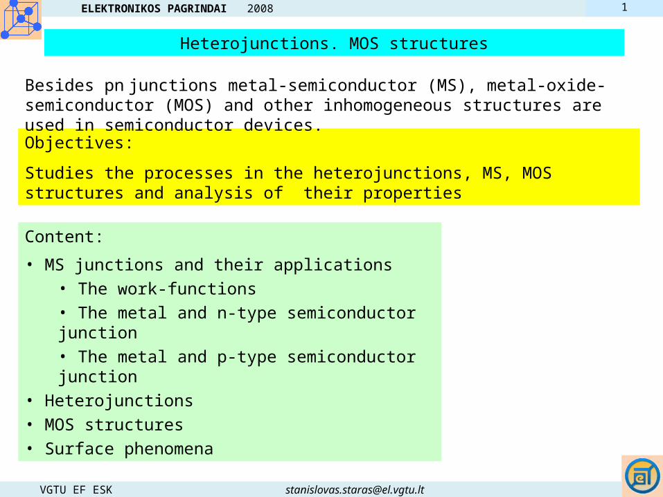
Heterojunctions. MOS structures
Objectives:
Studies the processes in the heterojunctions, MS, MOS structures and analysis of their properties
Content:
• MS junctions and their applications
• The work-functions
• The metal and n-type semiconductor junction
• The metal and p-type semiconductor junction
• Heterojunctions
• MOS structures
• Surface phenomena
Besides pn junctions metal-semiconductor (MS), metal-oxide-semiconductor (MOS) and other inhomogeneous structures are used in semiconductor devices.
ELEKTRONIKOS PAGRINDAI 2008
VGTU EF ESK [email protected]
1
MS structures
Historically the first practical semiconductor device was the MS diode.
It is possible to obtain both rectifying and non-rectifying MS junctions.
The non-rectifying junction has low ohmic drop regardless of the polarity of the externally applied voltage and it is called ohmic contact. All semiconductor devices need ohmic contacts to make connections to other devices or circuit elements.
Rectifying MS junctions have important device applications in high-frequency devices.
Let us examine the processes in the MS structures and discuss their properties and application.
Properties of metal-semiconductor structures are dependent on the work-functions of the materials being in contact and the type of the semiconductor.
ELEKTRONIKOS PAGRINDAI 2008
VGTU EF ESK [email protected]
2
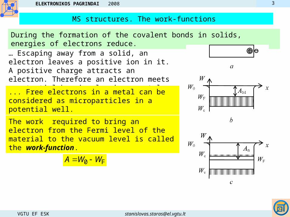
During the formation of the covalent bonds in solids, energies of electrons reduce.
… Escaping away from a solid, an electron leaves a positive ion in it. A positive charge attracts an electron. Therefore an electron meets a potential barrier leaving a metal.
The work required to bring an electron from the Fermi level of the material to the vacuum level is called the work-function.
F0 WWA
MS structures. The work-functions
... Free electrons in a metal can be considered as microparticles in a potential well.
ELEKTRONIKOS PAGRINDAI 2008
VGTU EF ESK [email protected]
3
Metal and n-type semiconductor junction
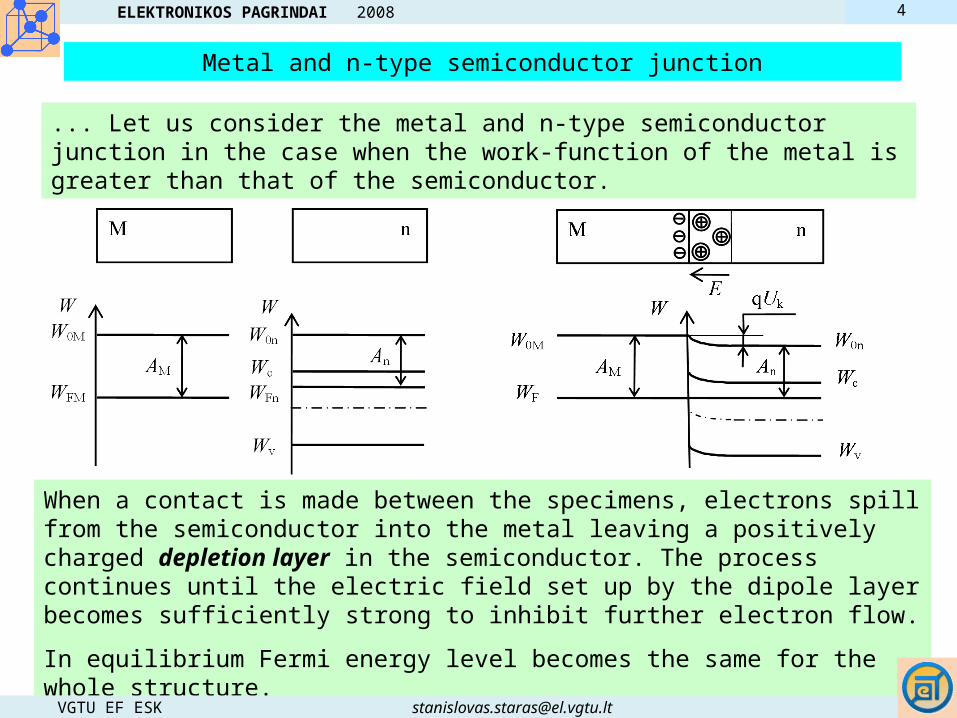
... Let us consider the metal and n-type semiconductor junction in the case when the work-function of the metal is greater than that of the semiconductor.
When a contact is made between the specimens, electrons spill from the semiconductor into the metal leaving a positively charged depletion layer in the semiconductor. The process continues until the electric field set up by the dipole layer becomes sufficiently strong to inhibit further electron flow.
In equilibrium Fermi energy level becomes the same for the whole structure.
ELEKTRONIKOS PAGRINDAI 2008
VGTU EF ESK [email protected]
4
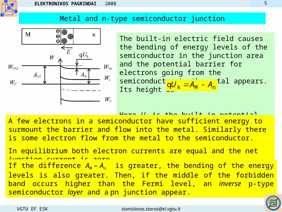
The built-in electric field causes the bending of energy levels of the semiconductor in the junction area and the potential barrier for electrons going from the semiconductor to the metal appears. Its height is
Here Uk is the built-in-potential.
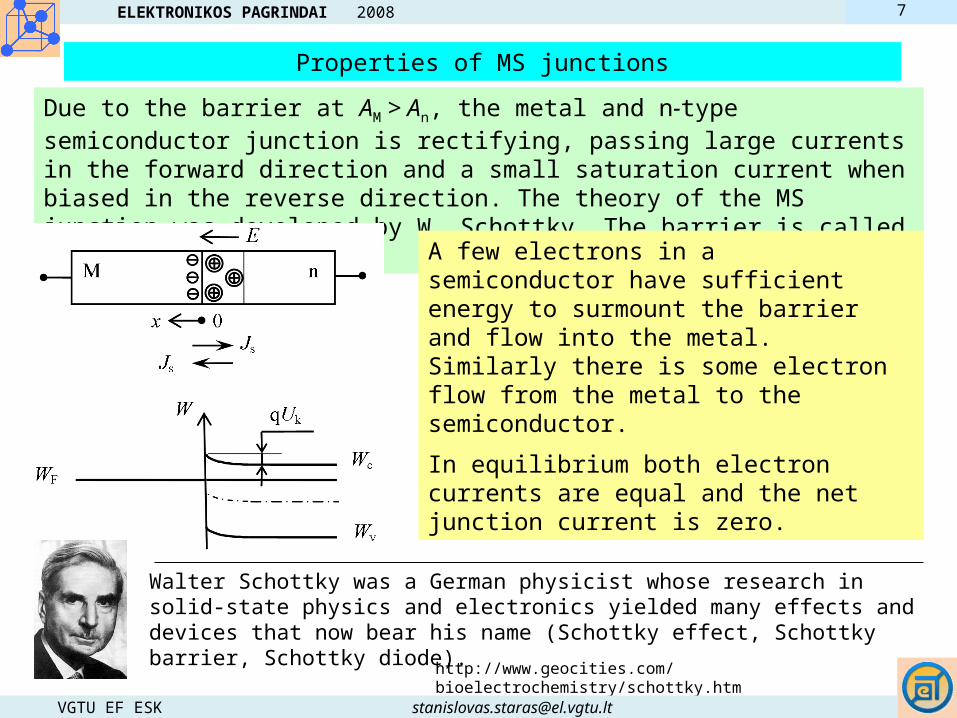
A few electrons in a semiconductor have sufficient energy to surmount the barrier and flow into the metal. Similarly there is some electron flow from the metal to the semiconductor.
In equilibrium both electron currents are equal and the net junction current is zero.
nMkq AAU
If the difference AM – An is greater, the bending of the energy levels is also greater. Then, if the middle of the forbidden band occurs higher than the Fermi level, an inverse p-type semiconductor layer and a pn junction appear.
Metal and n-type semiconductor junction
ELEKTRONIKOS PAGRINDAI 2008
VGTU EF ESK [email protected]
5
... At AM > An a depletion layer or the inverse layer and pn junction appear in the junction area.
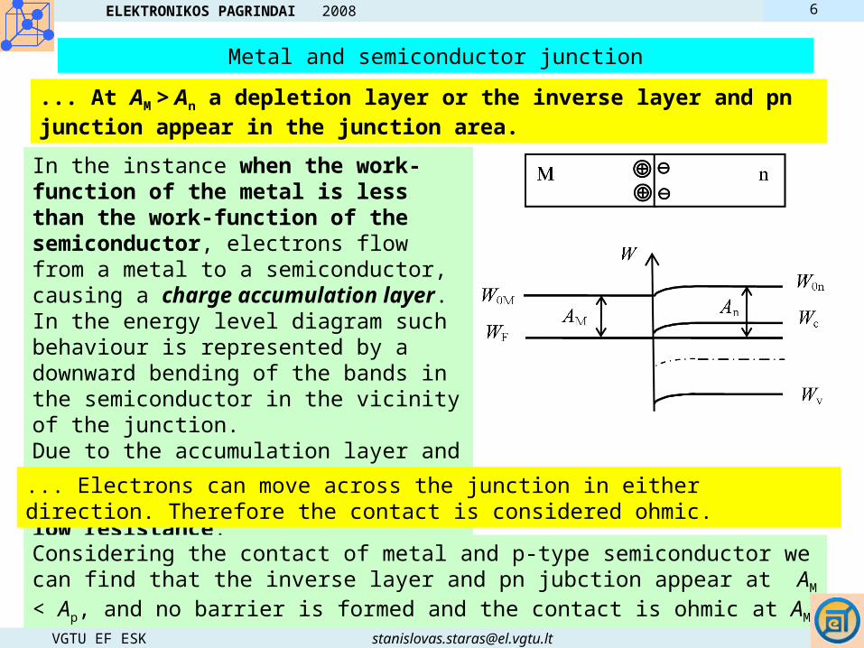
In the instance when the work-function of the metal is less than the work-function of the semiconductor, electrons flow from a metal to a semiconductor, causing a charge accumulation layer. In the energy level diagram such behaviour is represented by a downward bending of the bands in the semiconductor in the vicinity of the junction.Due to the accumulation layer and absence of the barrier in the semiconductor, the junction has low resistance.
Considering the contact of metal and p-type semiconductor we can find that the inverse layer and pn jubction appear at AM < Ap, and no barrier is formed and the contact is ohmic at AM > Ap.
Metal and semiconductor junction
... Electrons can move across the junction in either direction. Therefore the contact is considered ohmic.
ELEKTRONIKOS PAGRINDAI 2008
VGTU EF ESK [email protected]
6
Properties of MS junctions
Due to the barrier at AM > An, the metal and n-type semiconductor junction is rectifying, passing large currents in the forward direction and a small saturation current when biased in the reverse direction. The theory of the MS junction was developed by W. Schottky. The barrier is called Schottky barrier.
A few electrons in a semiconductor have sufficient energy to surmount the barrier and flow into the metal. Similarly there is some electron flow from the metal to the semiconductor.
In equilibrium both electron currents are equal and the net junction current is zero.
Walter Schottky was a German physicist whose research in solid-state physics and electronics yielded many effects and devices that now bear his name (Schottky effect, Schottky barrier, Schottky diode).
http://www.geocities.com/bioelectrochemistry/schottky.htm
ELEKTRONIKOS PAGRINDAI 2008
VGTU EF ESK [email protected]
7
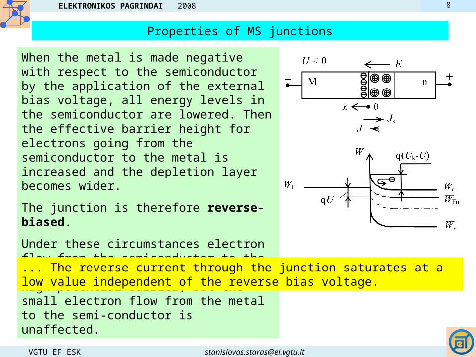
When the metal is made negative with respect to the semiconductor by the application of the external bias voltage, all energy levels in the semiconductor are lowered. Then the effective barrier height for electrons going from the semiconductor to the metal is increased and the depletion layer becomes wider.
The junction is therefore reverse-biased.
Under these circumstances electron flow from the semiconductor to the metal is entirely prohibited by the high potential barrier, but the small electron flow from the metal to the semi-conductor is unaffected.
Properties of MS junctions
... The reverse current through the junction saturates at a low value independent of the reverse bias voltage.
ELEKTRONIKOS PAGRINDAI 2008
VGTU EF ESK [email protected]
8
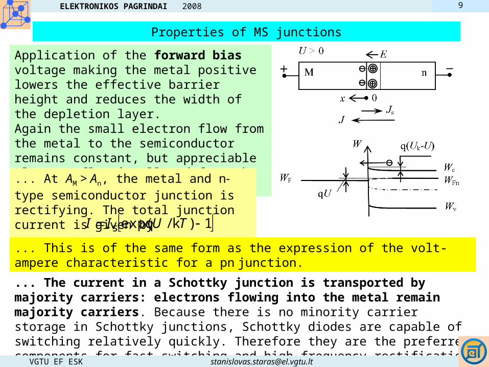
Application of the forward bias voltage making the metal positive lowers the effective barrier height and reduces the width of the depletion layer. Again the small electron flow from the metal to the semiconductor remains constant, but appreciable electron flow is allowed from the semiconductor into the metal.
... At AM > An, the metal and n-type semiconductor junction is rectifying. The total junction current is given by
1)k/qexp(s TUII
... This is of the same form as the expression of the volt-ampere characteristic for a pn junction.
Properties of MS junctions
... The current in a Schottky junction is transported by majority carriers: electrons flowing into the metal remain majority carriers. Because there is no minority carrier storage in Schottky junctions, Schottky diodes are capable of switching relatively quickly. Therefore they are the preferred components for fast switching and high-frequency rectification applications.
ELEKTRONIKOS PAGRINDAI 2008
VGTU EF ESK [email protected]
9

... Ohmic contacts are necessary for connection of terminals to regions of semiconductor devices.
... Aluminium is widely used for interconnec-tions in integrated circuits.
Aluminium in contact with silicon acts as a p-type impurity, and aluminium and p-type semiconductor contacts have low resistance.
Aluminium in contact with n-type material, however, would create a rectifying contact instead of the desired ohmic contact. In practice, therefore, contacts to the n-type material are made of special alloys or a layer of heavily doped n+ material is used to provide a low-potential transition between the semiconductor and the metal.
Properties of MS junctions
ELEKTRONIKOS PAGRINDAI 2008
VGTU EF ESK [email protected]
10
MS structures. Problem
The voltage of 0.4 V is applied to the n-type semiconductor and metal junction
and the current of 1 A flows across the junction at 300 K. The work-function of
the metal is 1.4 eV, and the work-function of the semiconductor is 1 eV. Find the
current across the junction after changing polarity of the voltage.
ELEKTRONIKOS PAGRINDAI 2008
VGTU EF ESK [email protected]
11
Heterojunctions
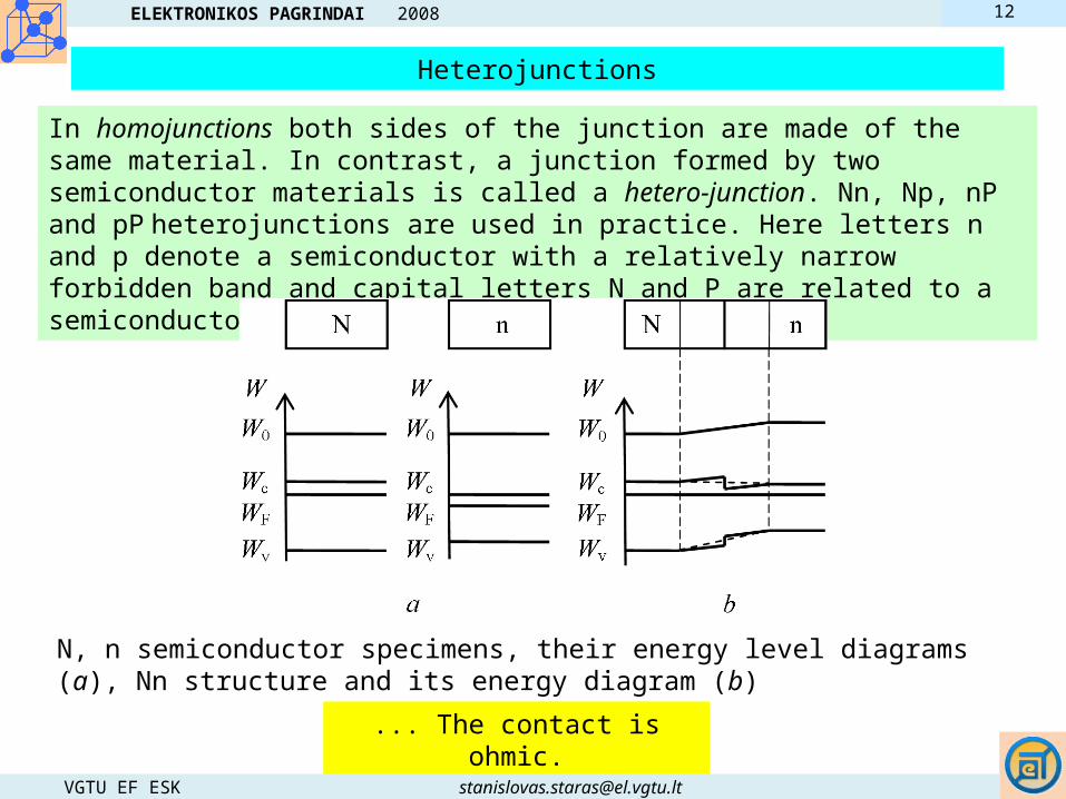
In homojunctions both sides of the junction are made of the same material. In contrast, a junction formed by two semiconductor materials is called a hetero-junction. Nn, Np, nP and pP heterojunctions are used in practice. Here letters n and p denote a semiconductor with a relatively narrow forbidden band and capital letters N and P are related to a semiconductor with a wider forbidden band.
N, n semiconductor specimens, their energy level diagrams (a), Nn structure and its energy diagram (b)
... The contact is ohmic.
ELEKTRONIKOS PAGRINDAI 2008
VGTU EF ESK [email protected]
12
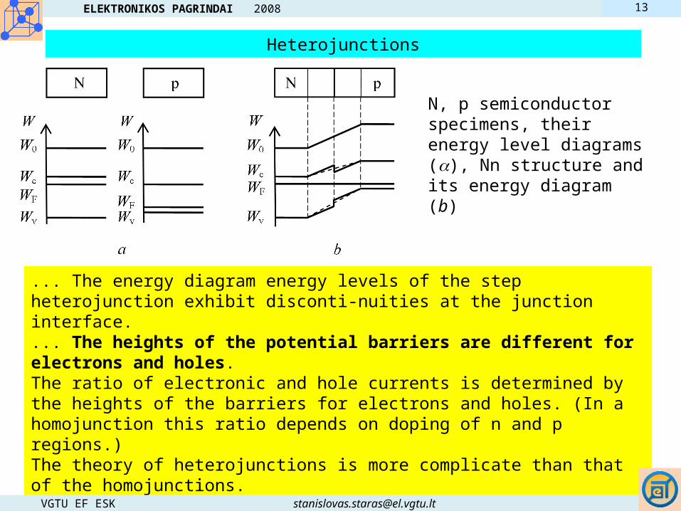
N, p semiconductor specimens, their energy level diagrams (), Nn structure and its energy diagram (b)
... The energy diagram energy levels of the step heterojunction exhibit disconti-nuities at the junction interface. ... The heights of the potential barriers are different for electrons and holes. The ratio of electronic and hole currents is determined by the heights of the barriers for electrons and holes. (In a homojunction this ratio depends on doping of n and p regions.)The theory of heterojunctions is more complicate than that of the homojunctions.Heterojunctions are widely used for semiconductor lasers and other optical electronic devices.
Heterojunctions
ELEKTRONIKOS PAGRINDAI 2008
VGTU EF ESK [email protected]
13
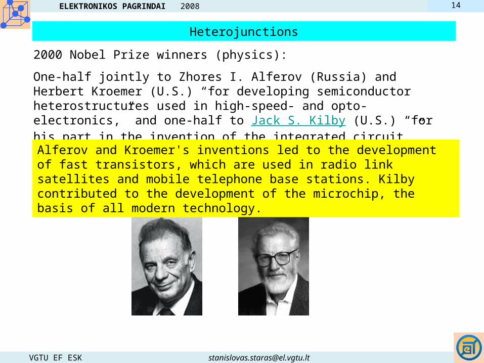
2000 Nobel Prize winners (physics):
One-half jointly to Zhores I. Alferov (Russia) and Herbert Kroemer (U.S.) “for developing semiconductor heterostructures used in high-speed- and opto-electronics,” and one-half to Jack S. Kilby (U.S.) “for his part in the invention of the integrated circuit.”
Heterojunctions
Alferov and Kroemer's inventions led to the development of fast transistors, which are used in radio link satellites and mobile telephone base stations. Kilby contributed to the development of the microchip, the basis of all modern technology.
ELEKTRONIKOS PAGRINDAI 2008
VGTU EF ESK [email protected]
14
MOS structures
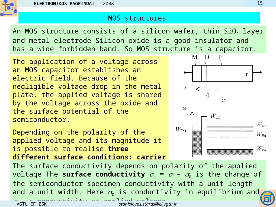
An MOS structure consists of a silicon wafer, thin SiO2 layer and metal electrode Silicon oxide is a good insulator and has a wide forbidden band. So MOS structure is a capacitor.
The application of a voltage across an MOS capacitor establishes an electric field. Because of the negligible voltage drop in the metal plate, the applied voltage is shared by the voltage across the oxide and the surface potential of the semiconductor.
Depending on the polarity of the applied voltage and its magnitude it is possible to realise three different surface conditions: carrier accumulation, carrier depletion and carrier inversion.
The surface conductivity depends on polarity of the applied voltage The surface conductivity s = – 0 is the change of the semiconductor specimen conductivity with a unit length and a unit width. Here 0 is conductivity in equilibrium and is conductivity at applied voltage.
ELEKTRONIKOS PAGRINDAI 2008
VGTU EF ESK [email protected]
15
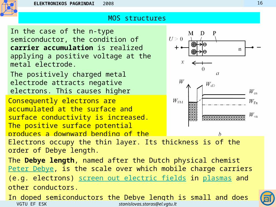
In the case of the n-type semiconductor, the condition of carrier accumulation is realized applying a positive voltage at the metal electrode.
The positively charged metal electrode attracts negative electrons. This causes higher electron density and lower hole density at the semicon-ductor surface compared with that of the bulk.
Consequently electrons are accumulated at the surface and surface conductivity is increased. The positive surface potential produces a downward bending of the energy bands
Electrons occupy the thin layer. Its thickness is of the order of Debye length.
The Debye length, named after the Dutch physical chemist Peter Debye, is the scale over which mobile charge carriers (e.g. electrons) screen out electric fields in plasmas and other conductors.
In doped semiconductors the Debye length is small and does not depend on voltage.
MOS structures
ELEKTRONIKOS PAGRINDAI 2008
VGTU EF ESK [email protected]
16
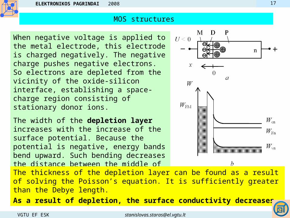
When negative voltage is applied to the metal electrode, this electrode is charged negatively. The negative charge pushes negative electrons. So electrons are depleted from the vicinity of the oxide-silicon interface, establishing a space-charge region consisting of stationary donor ions.
The width of the depletion layer increases with the increase of the surface potential. Because the potential is negative, energy bands bend upward. Such bending decreases the distance between the middle of the forbidden gap and Fermi level, indicating smaller electron density and smaller surface conductivity.
The thickness of the depletion layer can be found as a result of solving the Poisson’s equation. It is sufficiently greater than the Debye length.
As a result of depletion, the surface conductivity decreases.
MOS structures
ELEKTRONIKOS PAGRINDAI 2008
VGTU EF ESK [email protected]
17
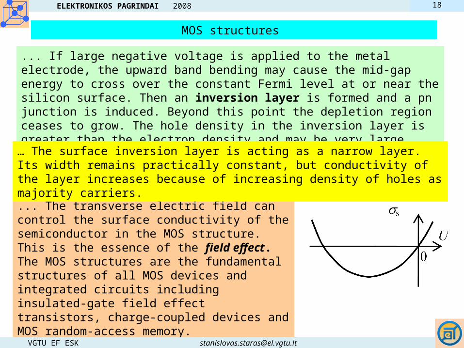
... If large negative voltage is applied to the metal electrode, the upward band bending may cause the mid-gap energy to cross over the constant Fermi level at or near the silicon surface. Then an inversion layer is formed and a pn junction is induced. Beyond this point the depletion region ceases to grow. The hole density in the inversion layer is greater than the electron density and may be very large.
... The transverse electric field can control the surface conductivity of the semiconductor in the MOS structure. This is the essence of the field effect.The MOS structures are the fundamental structures of all MOS devices and integrated circuits including insulated-gate field effect transistors, charge-coupled devices and MOS random-access memory.
MOS structures
… The surface inversion layer is acting as a narrow layer. Its width remains practically constant, but conductivity of the layer increases because of increasing density of holes as majority carriers.
ELEKTRONIKOS PAGRINDAI 2008
VGTU EF ESK [email protected]
18

Under the condition of carrier accumulation there is no depletion layer and the overall capacitance equals to C0.
Beyond strong inversion, the maximum space-charge width becomes constant. Then Cb and C are minimal and constant.
MOS structures
The capacitance of the MOS structure is a function of the voltage applied to the metal electrode and is also frequency dependent. Because of the surface-charge layer in silicon the overall capacitance C of an MOS structure may be represented as capacitance C0 with oxide as the dielectric material in series with space-charge-layer capacitance Cb.
ELEKTRONIKOS PAGRINDAI 2008
VGTU EF ESK [email protected]
19

With biasing voltage between the condition of carrier accumulation and strong inversion, the space-charge-layer is dependent on the reverse bias.
Its width increases with the increase of the bias voltage causing the decrease of space-charge-layer capacitance and overall capacitance.
Such capacitance-voltage characteristic can be obtained experimentally, if the measurement frequency is high.
... If the measurement frequency is low enough, the C-U curve will be changed because of carrier generation within the space-charge layer. The C-U curve at low frequency is given by the dashed line.
MOS structures
ELEKTRONIKOS PAGRINDAI 2008
VGTU EF ESK [email protected]
20
MOS structures containing p-type semiconductor have similar properties.
Carrier accumulation, carrier depletion and carrier inversion are possible.
The general rule can be formulated in this way.
If the polarity of the voltage applied to the metal layer is of the opposite polarity with respect to the majority carriers in the semiconductor, the charge accumulation layer appears.
If the polarity of the voltage applied to the metal layer is of the same polarity as the polarity of the majority carriers in the semiconductor, the depletion layer and the inversion layers become possible.
MOS structures
ELEKTRONIKOS PAGRINDAI 2008
VGTU EF ESK [email protected]
21
Surface phenomena
The surface states arise because the crystal periodicity ends at the surface and there is great likelihood for crystal damage and contamination caused by adsorbed impurity atoms or oxide layers at the surface.
The surface states behave as either electron or hole traps depending on the origin of the states.
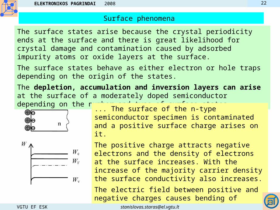
The depletion, accumulation and inversion layers can arise at the surface of a moderately doped semiconductor depending on the number and type of surface states.
... The surface of the n-type semiconductor specimen is contaminated and a positive surface charge arises on it.
The positive charge attracts negative electrons and the density of electrons at the surface increases. With the increase of the majority carrier density the surface conductivity also increases.
The electric field between positive and negative charges causes bending of energy levels at the surface.
ELEKTRONIKOS PAGRINDAI 2008
VGTU EF ESK [email protected]
22
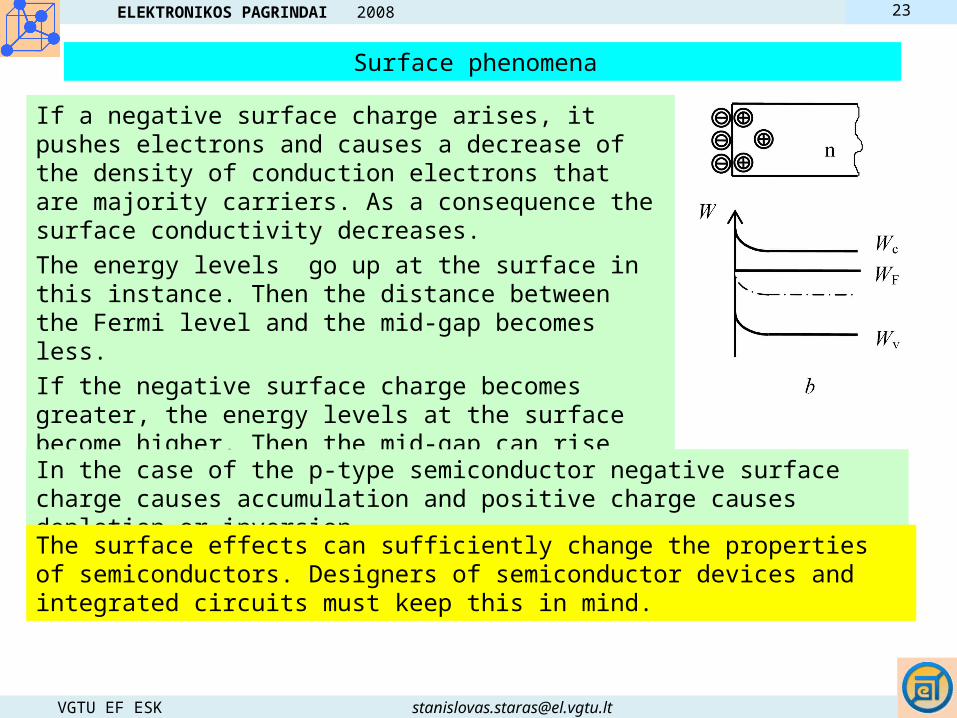
If a negative surface charge arises, it pushes electrons and causes a decrease of the density of conduction electrons that are majority carriers. As a consequence the surface conductivity decreases.
The energy levels go up at the surface in this instance. Then the distance between the Fermi level and the mid-gap becomes less.
If the negative surface charge becomes greater, the energy levels at the surface become higher. Then the mid-gap can rise higher than the Fermi level at the surface.
As a consequence a p-type layer and pn junction appear.
In the case of the p-type semiconductor negative surface charge causes accumulation and positive charge causes depletion or inversion.
The surface effects can sufficiently change the properties of semiconductors. Designers of semiconductor devices and integrated circuits must keep this in mind.
Surface phenomena
ELEKTRONIKOS PAGRINDAI 2008
VGTU EF ESK [email protected]
23
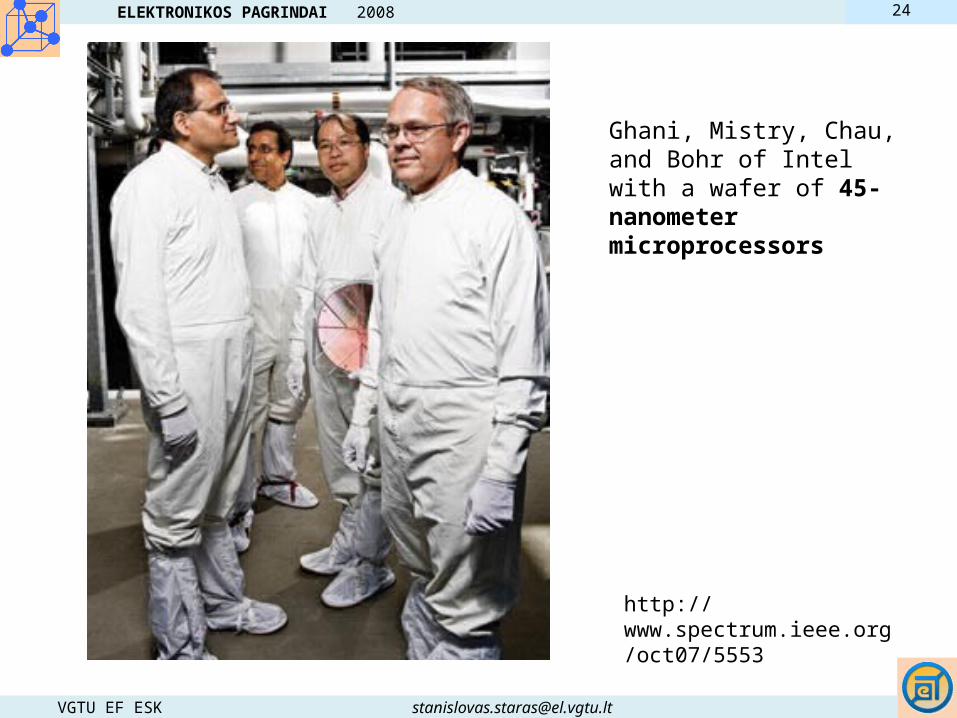
Ghani, Mistry, Chau, and Bohr of Intel with a wafer of 45-nanometer microprocessors
http://www.spectrum.ieee.org/oct07/5553
ELEKTRONIKOS PAGRINDAI 2008
VGTU EF ESK [email protected]
24