Embed Size (px)
Citation preview
Hexagonal boron nitride and 6H-SiC heterostructuresS. Majety, J. Li, W. P. Zhao, B. Huang, S. H. Wei et al. Citation: Appl. Phys. Lett. 102, 213505 (2013); doi: 10.1063/1.4808365 View online: http://dx.doi.org/10.1063/1.4808365 View Table of Contents: http://apl.aip.org/resource/1/APPLAB/v102/i21 Published by the American Institute of Physics. Additional information on Appl. Phys. Lett.Journal Homepage: http://apl.aip.org/ Journal Information: http://apl.aip.org/about/about_the_journal Top downloads: http://apl.aip.org/features/most_downloaded Information for Authors: http://apl.aip.org/authors
Hexagonal boron nitride and 6H-SiC heterostructures
S. Majety,1 J. Li,1 W. P. Zhao,1 B. Huang,2 S. H. Wei,2 J. Y. Lin,1 and H. X. Jiang1,a)
1Department of Electrical and Computer Engineering, Texas Tech University, Lubbock, Texas 79409, USA2National Renewable Energy Laboratory, 1617 Cole Boulevard, Golden, Colorado 80401, USA
(Received 24 April 2013; accepted 16 May 2013; published online 31 May 2013)
Hexagonal boron nitride (hBN) epilayers were grown on n-type 6H-SiC substrates via metal
organic chemical vapor deposition. X-ray diffraction measurements confirmed that the epilayers
are of single hexagonal phase. Photoluminescence (PL) studies revealed a dominant band edge
emission at around 5.5 eV, similar to the PL spectra of hBN epilayers grown on sapphire. The
current-voltage (I-V) characteristics of the hBN/6H-SiC heterostructure were measured and the
results were utilized to determine the band offsets of the hBN/6H-SiC heterojunctions. The
analysis yielded the conduction and valence band offsets (DEC and DEV) of the hBN/6H-SiC
heterointerface of about 2.3 and 0.7 (60.2) eV, respectively, giving a DEC/DEg value of around
76%. The measured band offsets are in reasonable agreement with values deduced from the band
alignments between hBN, AlN, and 6H-SiC obtained from independent experimental data and
theoretical calculations. VC 2013 AIP Publishing LLC. [http://dx.doi.org/10.1063/1.4808365]
Hexagonal boron nitride (hBN) has been the material of
heavy interest recently due to its unique physical properties,
including high thermal conductivity, chemical stability, neg-
ative electron affinity, and a large band gap (Eg� 6 eV).1–5
The reported low dielectric constant ðkÞ of �4 and high mass
density of 1.8–2.0 g/cm3 coupled with high breakdown field
(>4.4 MV/cm for hBN epilayers) and low leakage currents
make it a very attractive material for low-k applications.6–8
With the popularity that graphene has garnered, hBN has
also emerged as an ideal template and gate dielectric layer
for graphene. Lasing action in the deep UV (DUV) range
(�225 nm) has been demonstrated in bulk hBN crystals via
e-beam pumping,5 suggesting that it is a suitable material for
DUV photonic device applications. The hexagonal layered
structure of hBN increases the exciton binding energy and
the optical emission efficiency over 3D systems. Huang
et al. has recently established through group theory analysis
and first principle calculations that the strong band edge
emission in hBN originates from the abnormally strong p!p like transition and two-dimensional (2D) nature of hBN.9
The band edge photoluminescence (PL) intensity of hBN
was observed to be two orders of magnitude higher than that
of AlN which has a comparable band gap as hBN.7 The wa-
fer scale growth of good quality hBN epilayers could poten-
tially make it the material of choice for DUV photonic
devices which relied heavily on AlN till now. The ability to
dramatically reduce the p-type resistivity of hBN by Mg dop-
ing is another huge advantage over AlN and suggests the
possibility of achieving DUV optoelectronic devices with
high quantum efficiency.10
To expand our epitaxial growth studies beyond hBN on
sapphire substrates and AlGaN templates,7,10–12 here we
report on the synthesis of good quality hBN epilayers on
highly conductive n-type 6H-SiC (0001) substrates. Previous
studies on the growth of hBN layers were mostly confined to
sapphire, Ni(111), and silicon substrates with very limited
reports on the growth of hBN on SiC substrates.13,14 The
semiconducting properties of hBN/SiC heterostructures have
not been previously studied and are expected to open up
opportunities to design electronic and photonic devices with
very interesting applications.
Undoped hBN epilayers of thickness �0.5 lm were
grown using low pressure metal organic chemical vapor
deposition (MOCVD). The precursors for boron and nitro-
gen are triethyl-boron (TEB) and ammonia (NH3), respec-
tively. The growth was carried out on n-type 6H-SiC
(0001) on-axis substrates. The (0001) surface of SiC is the
Si terminated surface. The electrical resistivity of the
6H-SiC substrate is around 0.01 Xcm with a free electron
concentration around 5� 1018 cm�3. The growth of hBN
was carried out using hydrogen (H2) as a carrier gas to
transport the pre-cursors. The growth temperature of hBN
epilayers was 1300 �C with a low temperature buffer of
BN incorporated at 800 �C. Due to the crystal structure
mismatch between hBN and 6H-SiC (in-plane lattice con-
stants 2.5 A and 3.08 A, respectively), prior to epilayer
growth, a 20 nm BN buffer layer was first deposited on
6H-SiC substrate at 800 �C. Similar to the case in the con-
ventional III-nitride epitaxial growth, the functions of this
buffer layer include providing strain relieve from lattice
mismatch between the substrate and the subsequent hBN
epilayer. Furthermore, it was found that the use of the
buffer layer enhances significantly the adhesion of hBN
epilayers to the substrates. The schematic of the hBN/n-
SiC heterostructure is shown in the inset of Fig. 1. X-ray
diffraction (XRD) was used to investigate the crystalline
quality and lattice constant of the hBN layers. PL studies
were conducted on these samples using our deep UV laser
spectroscopy setup. The excitation laser with a photon
energy set at 6.3 eV for PL measurements was obtained
through the fourth harmonic generation of femtosecond
version of Ti:Sapphire laser. PL signal was dispersed using
a 1.3 m monochromator and detected by a photo-multiplier
tube (PMT).15
Figure 1 shows the XRD h-2h scan of the hBN/6H-SiC
heterostructure with a hBN (0002) reflection peak at 26.5�.a)[email protected]
0003-6951/2013/102(21)/213505/4/$30.00 VC 2013 AIP Publishing LLC102, 213505-1
APPLIED PHYSICS LETTERS 102, 213505 (2013)
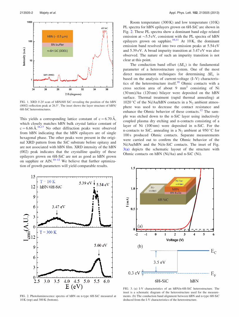
This yields a corresponding lattice constant of c¼ 6.70 A,
which closely matches hBN bulk crystal lattice constant of
c¼ 6.66 A.16,17 No other diffraction peaks were observed
from hBN indicating that the hBN epilayers are of single
hexagonal phase. The other peaks were present in the origi-
nal XRD pattern from the SiC substrate before epitaxy and
are not associated with hBN film. XRD intensity of the hBN
(002) peak indicates that the crystalline quality of these
epilayers grown on 6H-SiC are not as good as hBN grown
on sapphire or AlN.10–12 We believe that further optimiza-
tion of growth parameters will yield comparable results.
Room temperature (300 K) and low temperature (10 K)
PL spectra for hBN epilayers grown on 6H-SiC are shown in
Fig. 2. These PL spectra show a dominant band edge related
emission at �5.5 eV, consistent with the PL spectra of hBN
epilayers grown on sapphire.10,11 At 10 K, the dominant
emission band resolved into two emission peaks at 5.54 eV
and 5.39 eV. A broad impurity transition at 3.47 eV was also
observed. The nature of such an impurity transition is not
clear at this point.
The conduction band offset (DEc) is the fundamental
parameter of a heterostructure system. One of the most
direct measurement techniques for determining DEc is
based on the analysis of current-voltage (I–V) characteris-
tics of the heterostructure itself.18 Ohmic contacts with a
cross section area of about 9 mm2 consisting of Ni
(30 nm)/Au (120 nm) bilayer were deposited on the hBN
surface. Thermal treatment (rapid thermal annealing) at
1020 �C of the Ni/Au/hBN contacts in a N2 ambient atmos-
phere was used to decrease the contact resistance and
enhance the Ohmic behavior of these contacts.12 The sam-
ple was etched down to the n-SiC layer using inductively
coupled plasma dry etching and n-contacts consisting of a
layer of Ni (100 nm) were deposited in n-SiC. For the
n-contacts to SiC, annealing in a N2 ambient at 950 �C for
100 s produced Ohmic contacts. Separate measurements
were carried out to confirm the Ohmic behavior of the
Ni/Au/hBN and the Ni/n-SiC contacts. The inset of Fig.
3(a) depicts the schematic layout of the structure with
Ohmic contacts on hBN (Ni/Au) and n-SiC (Ni).
FIG. 1. XRD h-2h scan of hBN/6H SiC revealing the position of the hBN
(0002) reflection peak at 26.5�. The inset shows the layer structure of hBN/
6H-SiC heterostructures.
FIG. 2. Photoluminescence spectra of hBN on n-type 6H-SiC measured at
10 K (top) and 300 K (bottom).
FIG. 3. (a) I-V characteristics of an hBN/n-6H-SiC heterostructure. The
inset is a schematic diagram of the heterostructure used for the measure-
ments. (b) The conduction band alignment between hBN and n-type 6H-SiC
deduced from the I-V characteristics of the heterostructure.
213505-2 Majety et al. Appl. Phys. Lett. 102, 213505 (2013)
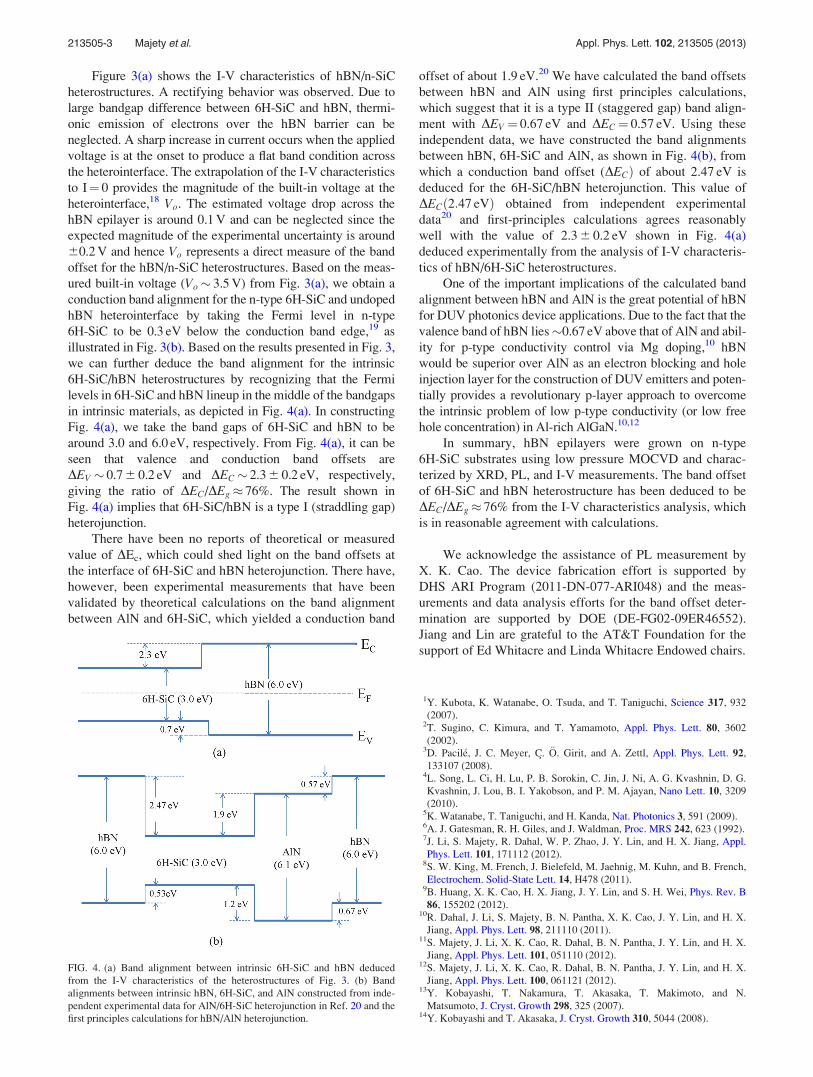
Figure 3(a) shows the I-V characteristics of hBN/n-SiC
heterostructures. A rectifying behavior was observed. Due to
large bandgap difference between 6H-SiC and hBN, thermi-
onic emission of electrons over the hBN barrier can be
neglected. A sharp increase in current occurs when the applied
voltage is at the onset to produce a flat band condition across
the heterointerface. The extrapolation of the I-V characteristics
to I¼ 0 provides the magnitude of the built-in voltage at the
heterointerface,18 Vo. The estimated voltage drop across the
hBN epilayer is around 0.1 V and can be neglected since the
expected magnitude of the experimental uncertainty is around
60.2 V and hence Vo represents a direct measure of the band
offset for the hBN/n-SiC heterostructures. Based on the meas-
ured built-in voltage (Vo� 3.5 V) from Fig. 3(a), we obtain a
conduction band alignment for the n-type 6H-SiC and undoped
hBN heterointerface by taking the Fermi level in n-type
6H-SiC to be 0.3 eV below the conduction band edge,19 as
illustrated in Fig. 3(b). Based on the results presented in Fig. 3,
we can further deduce the band alignment for the intrinsic
6H-SiC/hBN heterostructures by recognizing that the Fermi
levels in 6H-SiC and hBN lineup in the middle of the bandgaps
in intrinsic materials, as depicted in Fig. 4(a). In constructing
Fig. 4(a), we take the band gaps of 6H-SiC and hBN to be
around 3.0 and 6.0 eV, respectively. From Fig. 4(a), it can be
seen that valence and conduction band offsets are
DEV � 0.7 6 0.2 eV and DEC� 2.3 6 0.2 eV, respectively,
giving the ratio of DEC/DEg� 76%. The result shown in
Fig. 4(a) implies that 6H-SiC/hBN is a type I (straddling gap)
heterojunction.
There have been no reports of theoretical or measured
value of DEc, which could shed light on the band offsets at
the interface of 6H-SiC and hBN heterojunction. There have,
however, been experimental measurements that have been
validated by theoretical calculations on the band alignment
between AlN and 6H-SiC, which yielded a conduction band
offset of about 1.9 eV.20 We have calculated the band offsets
between hBN and AlN using first principles calculations,
which suggest that it is a type II (staggered gap) band align-
ment with DEV ¼ 0.67 eV and DEC¼ 0.57 eV. Using these
independent data, we have constructed the band alignments
between hBN, 6H-SiC and AlN, as shown in Fig. 4(b), from
which a conduction band offset (DECÞ of about 2.47 eV is
deduced for the 6H-SiC/hBN heterojunction. This value of
DECð2:47 eVÞ obtained from independent experimental
data20 and first-principles calculations agrees reasonably
well with the value of 2.3 6 0.2 eV shown in Fig. 4(a)
deduced experimentally from the analysis of I-V characteris-
tics of hBN/6H-SiC heterostructures.
One of the important implications of the calculated band
alignment between hBN and AlN is the great potential of hBN
for DUV photonics device applications. Due to the fact that the
valence band of hBN lies�0.67 eV above that of AlN and abil-
ity for p-type conductivity control via Mg doping,10 hBN
would be superior over AlN as an electron blocking and hole
injection layer for the construction of DUV emitters and poten-
tially provides a revolutionary p-layer approach to overcome
the intrinsic problem of low p-type conductivity (or low free
hole concentration) in Al-rich AlGaN.10,12
In summary, hBN epilayers were grown on n-type
6H-SiC substrates using low pressure MOCVD and charac-
terized by XRD, PL, and I-V measurements. The band offset
of 6H-SiC and hBN heterostructure has been deduced to be
DEC/DEg� 76% from the I-V characteristics analysis, which
is in reasonable agreement with calculations.
We acknowledge the assistance of PL measurement by
X. K. Cao. The device fabrication effort is supported by
DHS ARI Program (2011-DN-077-ARI048) and the meas-
urements and data analysis efforts for the band offset deter-
mination are supported by DOE (DE-FG02-09ER46552).
Jiang and Lin are grateful to the AT&T Foundation for the
support of Ed Whitacre and Linda Whitacre Endowed chairs.
1Y. Kubota, K. Watanabe, O. Tsuda, and T. Taniguchi, Science 317, 932
(2007).2T. Sugino, C. Kimura, and T. Yamamoto, Appl. Phys. Lett. 80, 3602
(2002).3D. Pacil�e, J. C. Meyer, C. €O. Girit, and A. Zettl, Appl. Phys. Lett. 92,
133107 (2008).4L. Song, L. Ci, H. Lu, P. B. Sorokin, C. Jin, J. Ni, A. G. Kvashnin, D. G.
Kvashnin, J. Lou, B. I. Yakobson, and P. M. Ajayan, Nano Lett. 10, 3209
(2010).5K. Watanabe, T. Taniguchi, and H. Kanda, Nat. Photonics 3, 591 (2009).6A. J. Gatesman, R. H. Giles, and J. Waldman, Proc. MRS 242, 623 (1992).7J. Li, S. Majety, R. Dahal, W. P. Zhao, J. Y. Lin, and H. X. Jiang, Appl.
Phys. Lett. 101, 171112 (2012).8S. W. King, M. French, J. Bielefeld, M. Jaehnig, M. Kuhn, and B. French,
Electrochem. Solid-State Lett. 14, H478 (2011).9B. Huang, X. K. Cao, H. X. Jiang, J. Y. Lin, and S. H. Wei, Phys. Rev. B
86, 155202 (2012).10R. Dahal, J. Li, S. Majety, B. N. Pantha, X. K. Cao, J. Y. Lin, and H. X.
Jiang, Appl. Phys. Lett. 98, 211110 (2011).11S. Majety, J. Li, X. K. Cao, R. Dahal, B. N. Pantha, J. Y. Lin, and H. X.
Jiang, Appl. Phys. Lett. 101, 051110 (2012).12S. Majety, J. Li, X. K. Cao, R. Dahal, B. N. Pantha, J. Y. Lin, and H. X.
Jiang, Appl. Phys. Lett. 100, 061121 (2012).13Y. Kobayashi, T. Nakamura, T. Akasaka, T. Makimoto, and N.
Matsumoto, J. Cryst. Growth 298, 325 (2007).14Y. Kobayashi and T. Akasaka, J. Cryst. Growth 310, 5044 (2008).
FIG. 4. (a) Band alignment between intrinsic 6H-SiC and hBN deduced
from the I-V characteristics of the heterostructures of Fig. 3. (b) Band
alignments between intrinsic hBN, 6H-SiC, and AlN constructed from inde-
pendent experimental data for AlN/6H-SiC heterojunction in Ref. 20 and the
first principles calculations for hBN/AlN heterojunction.
213505-3 Majety et al. Appl. Phys. Lett. 102, 213505 (2013)

15K. B. Nam, J. Li, M. L. Nakarmi, J. Y. Lin, and H. X. Jiang, Appl. Phys.
Lett. 84, 5264 (2004).16S. L. Rumyantsev, M. E. Levinshtein, A. D. Jackson, S. N. Mohammmad,
G. L. Harris, M. G. Spencer, and M. S. Shur, in Properties of AdvancedSemiconductor Materials GaN, AlN, InN, BN, SiC, SiGe, edited by M. E.
Levinshtein, S. L. Rumyantsev, and M. S. Shur (John Wiley and Sons,
Inc., New York, 2001), pp. 67–92.
17R. W. Lynch and H. G. J. Drickamer, J. Chem. Phys. 44, 181 (1966).18S. L. Feng, J. Krynicki, V. Donchev, J. C. Bourgoin, M. Di Forte-Poisson,
C. Brylinski, S. Delage, H. Blanck, and S. Alaya, Semicond. Sci. Technol.
8, 2092 (1993).19Z. Sitar, M. J. Paisley, D. K. Smith, and R. E. Davis, Rev. Sci. Instrum. 61,
2407 (1990).20J. Choi and J. P. Chang, J. Appl. Phys. 98, 093513 (2005).
213505-4 Majety et al. Appl. Phys. Lett. 102, 213505 (2013)