Embed Size (px)
Citation preview
Published in Organic Electronics (2011) 12, 1903-1908
1
High charge-carrier mobilities in blends of poly(triarylamine) and TIPS-
pentacene leading to better performing X-ray sensors
Akarin Intaniwet*, Joseph L. Keddie, Maxim Shkunov and Paul J. Sellin
Department of Physics, University of Surrey, Guildford, Surrey, GU2 7XH (UK)
Advanced Technology Institute, University of Surrey, Guildford, Surrey, GU2 7XH (UK)
E-mail: [email protected]
Tel: +44 1483 686803
Fax: +44 1483 686781
* Current address: Energy Research Center, Maejo University, Chiang Mai, Thailand 50290
Abstract
A new class of X-ray sensor – in which there is a blend of poly(triarylamine) (PTAA) and
6,13-bis(triisopropylsilylethynyl) (TIPS)-pentacene in the active layer of a diode structure –
has been developed. The crystalline pentacene provides a fast route for charge carriers and
leads to enhanced performance of the sensor. The first time-of-flight charge-carrier mobility
measurement of this blend is reported. The mobility of PTAA and TIPS-pentacene in a 1:25
molar ratio was found to be 2.2×10⁻⁵
cm2 V
-1 s
-1 (averaged for field strengths between 3×10
4
and 4×10⁵ Vcm
-1), which is about 17 times higher than that obtained in PTAA over the same
range of field strengths. This higher mobility is correlated with a four-fold increase in the X-
ray detection sensitivity in the PTAA:TIPS-pentacene devices.
Keywords: Sensors, Mobility, X-ray Detection, Charge Transport, Time-of-Flight
Photocurrent, PTAA, TIPS pentacene
Published in Organic Electronics (2011) 12, 1903-1908
2
1. Introduction
Numerous electronic devices, including field effect transistors [1], light-emitting
diodes [2], photovoltaic cells [3], and radiation sensors [4, 5],
have in recent years employed
organic materials as the active component. These devices share one common feature in that
their efficiency depends strongly on the transport of charge carriers. The performance of
electronic devices using typical semiconducting polymers is limited by the relatively low
charge-carrier mobility of the active material (in the range from 10-5
to 10-2
cm2 V
-1 s
-1) [6-9]
in comparison to conventional materials. To achieve a higher level of performance, there is a
need for a material that provides the good film formation and ease of processing offered by
conjugated polymers but that also possesses a high charge-carrier mobility.
Small molecule organic semiconductors, such as 6,13-bis(triisopropylsilylethynyl)
(TIPS) pentacene, have been found to exhibit a very high charge carrier mobility (> 1 cm2 V
-1
s-1
) [10, 11] because the molecules arrange into a well-organised polycrystalline structure [12,
13]. However, difficulties in the solution processing of TIPS-pentacene, stemming from the
anisotropy of crystal formation [14], restricts its use in large-area deposition. Blending
conjugated polymers with TIPS-pentacene, which brings together their advantageous
properties to create a composite with good film formation and processability coupled with
high charge-carrier mobility, is a logical tactic to address the materials’ limitations. Blends of
conjugated polymers and small molecules, such as poly(triarylamine) (PTAA) and TIPS-
pentacene, have previously been studied in relation to field-effect transistor applications [15],
and a better performance was observed in this type of device when blends were used. But
whether diode structures - as employed in solar cells, LEDs, and sensors - could benefit from
the use of polymer/small molecule blends is still the subject of investigation.
Radiation sensors are an emerging application for semiconducting polymers [16]. The
use of polymers – in the place of conventional inorganic semiconductors - opens up the
possibility for large-area fabrication of sensors using low-cost, wet processing techniques,
Published in Organic Electronics (2011) 12, 1903-1908
3
such as spin-casting, spray-casting, ink-jet or roll-to-roll printing [17]. Radiation sensors
made from polymers exhibit greater mechanical flexibility in comparison to inorganic solids
[5]. Furthermore, the elemental composition of most polymers (C, H, N and O) makes them
an ideal candidate for dosimeters in medical applications, in which the detector requires a
“human tissue-equivalent” interaction with radiation. (The average atomic number of muscle
tissue is 7.4 [18].) Although radiotherapy and medical applications would benefit greatly from
the improved accuracy of tissue-equivalent dosimeters, there are currently no low-cost, large-
area devices with tissue-equivalence available.
Here, we present the first-ever measured charge transport properties of PTAA:TIPS-
pentacene blends using a time-of-flight (TOF) photocurrent measurement technique. We
correlate the raised mobility of the device with a four-fold increase in the X-ray detection
sensitivity. Our results point to benefits in using TIPS-pentacene/polymer blends in
applications that require high charge transport, such as light-emitting diodes, solar cells, and
light sensors, to raise their performance to a higher level.
2. Materials and Methods
The sensors employ layers (ca. 10 µm thick) of the polymer/molecule blend in a diode
geometry. The details of the device preparation can be found elsewhere [19, 20]. Briefly,
slides of ITO-coated glass (Delta Technology Ltd., USA (CB-60IN)) were cleaned with
acetone and deionised water. A 3 wt% solution of PTAA (with an average molecular weight
of 31 kg/mol.) was prepared in toluene (99.99% purity, Sigma Aldrich). Various
concentrations TIPS pentacene (Sigma-Aldrich) were then added to the solution. It was
homogenized for 10 minutes by stirring. Five different solutions were made: pure PTAA and
PTAA blended with TIPS-pentacene with PTAA:TIPS molar ratios of 1:1, 1:10, 1:17 and
1:25. The solutions were spin-cast at 50 rpm for 30 s onto a clean substrate to provide a single
layer of polymer. The films were dried under atmospheric conditions. Vacuum annealing was
Published in Organic Electronics (2011) 12, 1903-1908
4
then performed at 100 °C for 12 hours at pressure of 10-3
mbar, ensuring the temperature was
kept below the solid-to-solid phase transition temperature of TIPS-pentacene at 124 °C [21].
Then, the thickness and average surface roughness of the active layer was measured using
profilometry (Dektak Veeco). The device fabrication was completed by thermal evaporation
of thin aluminum contacts on top of the active layer to create a Schottky contact.
A Leica DM 2500P microscope was employed to take polarized optical images. For
energy dispersive X-ray analysis, an electron beam (Hitachi S-3200N electron microscope)
with accelerating voltage of 20 kV and an X-ray detector (silicon drift detector, Oxford
Instruments) was used.
For TOF measurements, an Al contact thickness of 50 nm and area of 9.6 mm2 was
deposited by thermal evaporation. The sample was held in a vacuum-tight steel box and was
illuminated through the semi-transparent Al electrode. The 10 ns, 355 nm pulse of a Nd:YAG
laser (Surelite Lasers, Continuum) was chosen to induce the optical excitation of the charge
carriers. The intensity of the laser was attenuated by a neutral density filter in order to
minimize the space-charge effect. To limit charge injection, the device was operated under a
reverse bias by applying a negative voltage to the ITO electrode through a blocking resistor
(10 kΩ). The resulting photocurrent pulses were recorded using a digital oscilloscope with a
50 Ω input terminal (Tektronix TDS 3032). Signal averaging and dark current subtraction
were carried out to improve the quality of the data. The TOF experiments were performed in
the dark, at room temperature, and under vacuum (3×10⁻¹
mbar).
For X-ray photocurrent measurements, Al top contacts with a thickness of 100 nm and
an area of 25 mm2 were deposited via thermal evaporation. To prevent oxidation, the sensors
were dip-coated in molten paraffin wax to create a barrier coating. The sensors were irradiated
by 17.5 keV Kα X-rays from a molybdenum target X-ray tube (XF50 11, Oxford instruments,
UK). While operating in a reverse bias, the sensor was exposed to the X-ray beam through the
metal top electrode. The induced photocurrent was then measured using a voltage source-
Published in Organic Electronics (2011) 12, 1903-1908
5
picoammeter (487, Keithley Instruments, UK). The dark current was subtracted from the
measured X-ray photocurrent in order to provide a corrected value of the photocurrent.
During exposure, the sensors were mounted in a steel box, in the dark and at room
temperature, 10 cm from the X-ray source. Sensor sensitivity was calculated from the slope of
a graph of X-ray photocurrent against dose rate and dividing by the active volume under the
contact (see Supplementary Data, Figures 1A and B) [5].
3. Results and Discussion
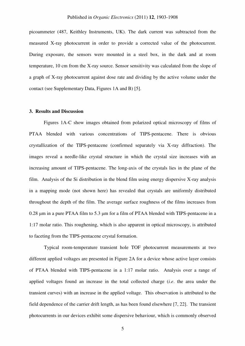
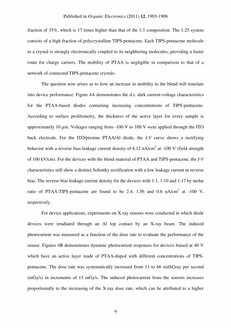
Figures 1A-C show images obtained from polarized optical microscopy of films of
PTAA blended with various concentrations of TIPS-pentacene. There is obvious
crystallization of the TIPS-pentacene (confirmed separately via X-ray diffraction). The
images reveal a needle-like crystal structure in which the crystal size increases with an
increasing amount of TIPS-pentacene. The long-axis of the crystals lies in the plane of the
film. Analysis of the Si distribution in the blend film using energy dispersive X-ray analysis
in a mapping mode (not shown here) has revealed that crystals are uniformly distributed
throughout the depth of the film. The average surface roughness of the films increases from
0.28 µm in a pure PTAA film to 5.3 µm for a film of PTAA blended with TIPS-pentacene in a
1:17 molar ratio. This roughening, which is also apparent in optical microscopy, is attributed
to faceting from the TIPS-pentacene crystal formation.
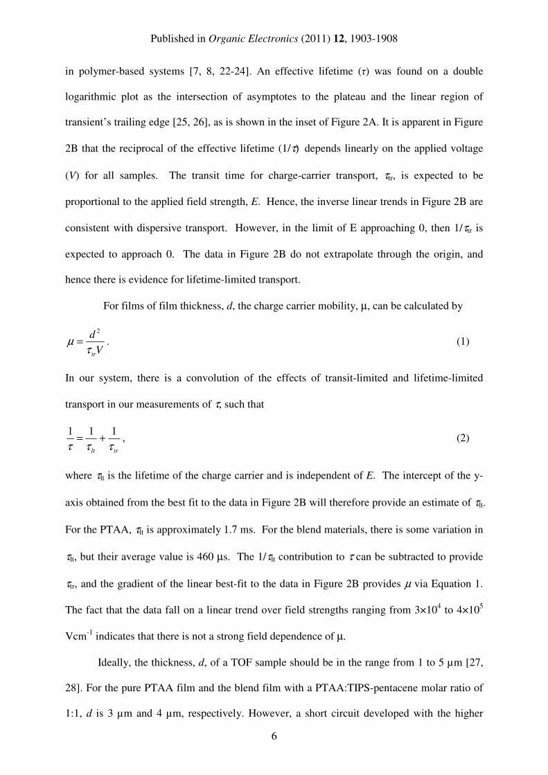
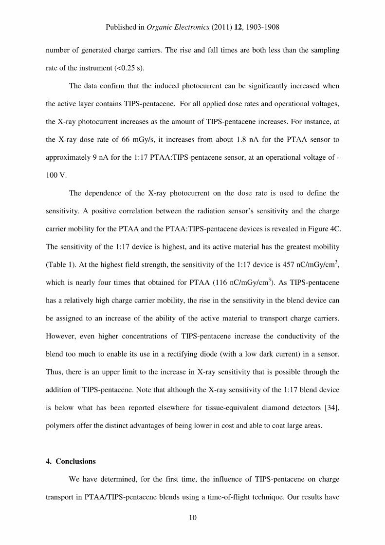
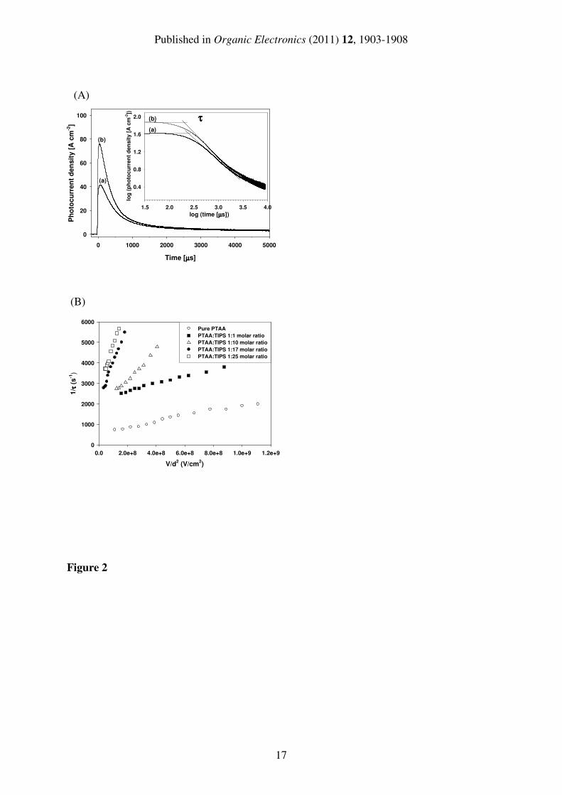
Typical room-temperature transient hole TOF photocurrent measurements at two
different applied voltages are presented in Figure 2A for a device whose active layer consists
of PTAA blended with TIPS-pentacene in a 1:17 molar ratio. Analysis over a range of
applied voltages found an increase in the total collected charge (i.e. the area under the
transient curves) with an increase in the applied voltage. This observation is attributed to the
field dependence of the carrier drift length, as has been found elsewhere [7, 22]. The transient
photocurrents in our devices exhibit some dispersive behaviour, which is commonly observed
Published in Organic Electronics (2011) 12, 1903-1908
6
in polymer-based systems [7, 8, 22-24]. An effective lifetime (τ) was found on a double
logarithmic plot as the intersection of asymptotes to the plateau and the linear region of
transient’s trailing edge [25, 26], as is shown in the inset of Figure 2A. It is apparent in Figure
2B that the reciprocal of the effective lifetime (1/τ) depends linearly on the applied voltage
(V) for all samples. The transit time for charge-carrier transport, τtr, is expected to be
proportional to the applied field strength, E. Hence, the inverse linear trends in Figure 2B are
consistent with dispersive transport. However, in the limit of E approaching 0, then 1/τtr is
expected to approach 0. The data in Figure 2B do not extrapolate through the origin, and
hence there is evidence for lifetime-limited transport.
For films of film thickness, d, the charge carrier mobility, µ, can be calculated by
V
d
trτµ
2
= . (1)
In our system, there is a convolution of the effects of transit-limited and lifetime-limited
transport in our measurements of τ, such that
trlt τττ
111+= , (2)
where τlt is the lifetime of the charge carrier and is independent of E. The intercept of the y-
axis obtained from the best fit to the data in Figure 2B will therefore provide an estimate of τlt.
For the PTAA, τlt is approximately 1.7 ms. For the blend materials, there is some variation in
τlt, but their average value is 460 µs. The 1/τlt contribution to τ can be subtracted to provide
τtr, and the gradient of the linear best-fit to the data in Figure 2B provides µ via Equation 1.
The fact that the data fall on a linear trend over field strengths ranging from 3×10⁴ to 4×10
5
Vcm-1
indicates that there is not a strong field dependence of µ.
Ideally, the thickness, d, of a TOF sample should be in the range from 1 to 5 µm [27,
28]. For the pure PTAA film and the blend film with a PTAA:TIPS-pentacene molar ratio of
1:1, d is 3 µm and 4 µm, respectively. However, a short circuit developed with the higher
Published in Organic Electronics (2011) 12, 1903-1908
7
concentrations of TIPS-pentacene in thin devices, because of the high conductivity of the
TIPS-pentacene and possible film imperfections. Therefore, in order to avoid this problem,
thicker films were used in the TOF experiments for the 1:10, 1:17 and 1:25 samples (8, 12 and
12 µm, respectively). Furthermore, according to profilometry analysis, there is a large
variation of the thickness in the 1:10, 1:17 and 1:25 sample because of the crystallization of
the TIPS-pentacene leading to a range of crystal sizes, especially in the 1:17 and 1:25 samples.
Hence, it should be noted that these are only average thicknesses.
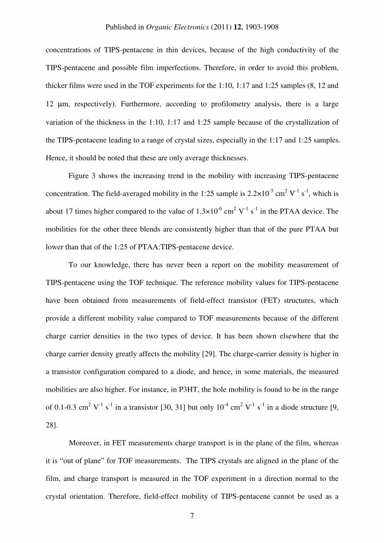
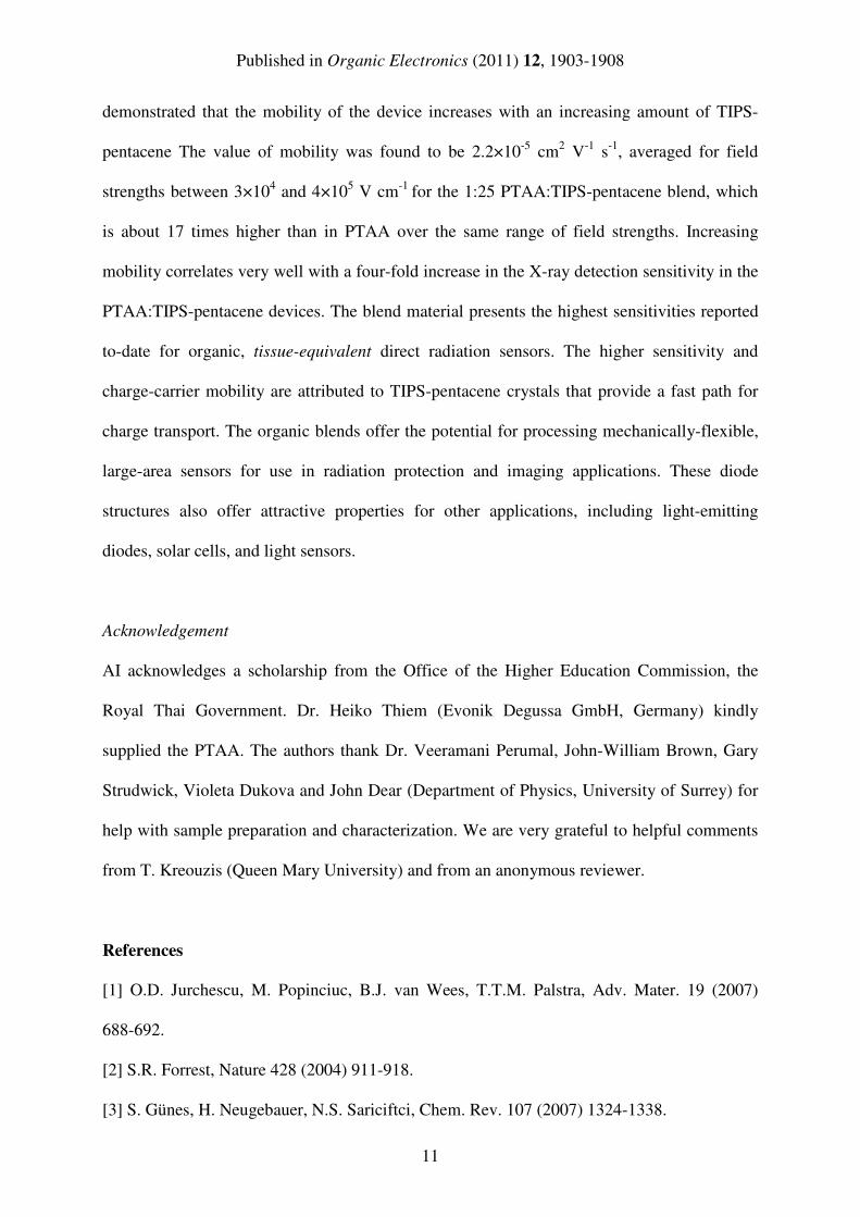
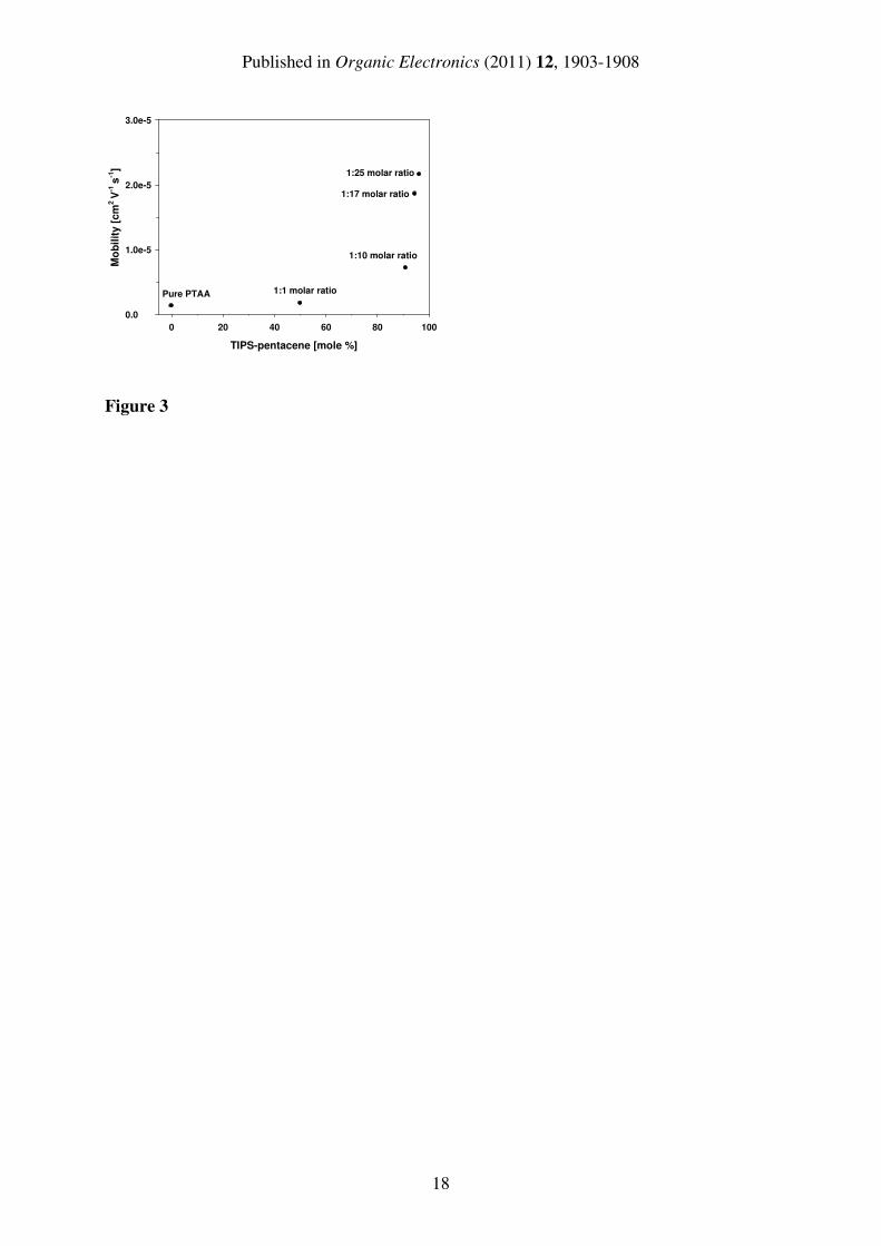
Figure 3 shows the increasing trend in the mobility with increasing TIPS-pentacene
concentration. The field-averaged mobility in the 1:25 sample is 2.2×10⁻⁵
cm2 V
-1 s
-1, which is
about 17 times higher compared to the value of 1.3×10⁻⁶
cm2 V
-1 s
-1 in the PTAA device. The
mobilities for the other three blends are consistently higher than that of the pure PTAA but
lower than that of the 1:25 of PTAA:TIPS-pentacene device.
To our knowledge, there has never been a report on the mobility measurement of
TIPS-pentacene using the TOF technique. The reference mobility values for TIPS-pentacene
have been obtained from measurements of field-effect transistor (FET) structures, which
provide a different mobility value compared to TOF measurements because of the different
charge carrier densities in the two types of device. It has been shown elsewhere that the
charge carrier density greatly affects the mobility [29]. The charge-carrier density is higher in
a transistor configuration compared to a diode, and hence, in some materials, the measured
mobilities are also higher. For instance, in P3HT, the hole mobility is found to be in the range
of 0.1-0.3 cm2 V
-1 s
-1 in a transistor [30, 31] but only 10
-4 cm
2 V
-1 s
-1 in a diode structure [9,
28].
Moreover, in FET measurements charge transport is in the plane of the film, whereas
it is “out of plane” for TOF measurements. The TIPS crystals are aligned in the plane of the
film, and charge transport is measured in the TOF experiment in a direction normal to the
crystal orientation. Therefore, field-effect mobility of TIPS-pentacene cannot be used as a
Published in Organic Electronics (2011) 12, 1903-1908
8
reference value for measurements in a diode structure, as in solar cells or sensors. Hamilton et
al. have reported the field-effect mobility value in the linear regime of about 0.7 cm2 V
-1 s
-1
(1.1 cm2 V
-1 s
-1 in the saturation regime) for the 1:1 by weight (1:50 molar ratio) of the
PTAA:TIPS-pentacene blend system [15]. Based on their argument, the mobility of the blend
system in the diode configuration is expected to be three orders of magnitude lower than in
the field-effect structure or about 7×10⁻⁴
cm2 V
-1 s
-1. This number is about 30 times greater
than the field-averaged mobility value found in our 1:25 PTAA:TIPS-pentacene device:
2.2×10⁻⁵
cm2 V
-1 s
-1.
Charge transport in conjugated polymer systems occurs through the hopping of charge
carriers from one site to another. Barard et al. [22] have employed the correlated disorder
model [32,33] to analyse the time-of-flight mobility data of a PTAA-based device. The effect
of the positional disorder was found to be greater than the energetic disorder at room
temperature and the mobility showed a weak negative field dependence. A large amount of
positional disorder in our device could come from the microstructure of the PTAA:TIPS-
pentacene blend film. In the optical images (Figure 1), it is apparent that TIPS-pentacene is
crystallised and forms ordered regions when the film is left to dry at room temperature. The
ordered TIPS-pentacene crystals are embedded in the PTAA amorphous phase, creating a
large PTAA/TIPS-pentacene interface. Due to better electronic coupling, the mobility in the
TIPS-pentacene crystals is significantly higher than in the amorphous PTAA phase.
It is apparent in Figure 3 that the introduction of TIPS-pentacene into PTAA has
clearly resulted in an increase in the mobility of the device. At higher TIPS-pentacene
concentrations, the mobility increases sharply. An increase in the mobility with increasing
TIPS-pentacene concentration is expected from a shift of charge transport domination from
PTAA to TIPS-pentacene, when the latter phase occupies a greater volume fraction. If the
densities of the two phases are approximated as being equal, then weight fraction will equal
the volume fraction. It can be estimated that the 1:25 composition will have a crystal volume
Published in Organic Electronics (2011) 12, 1903-1908
9
fraction of 35%, which is 17 times higher than that of the 1:1 composition. The 1:25 system
consists of a high fraction of polycrystalline TIPS-pentacene. Each TIPS-pentacene molecule
in a crystal is strongly electronically coupled to its neighboring molecules, providing a faster
route for charge carriers. The mobility of PTAA is negligible in comparison to that of a
network of connected TIPS-pentacene crystals.
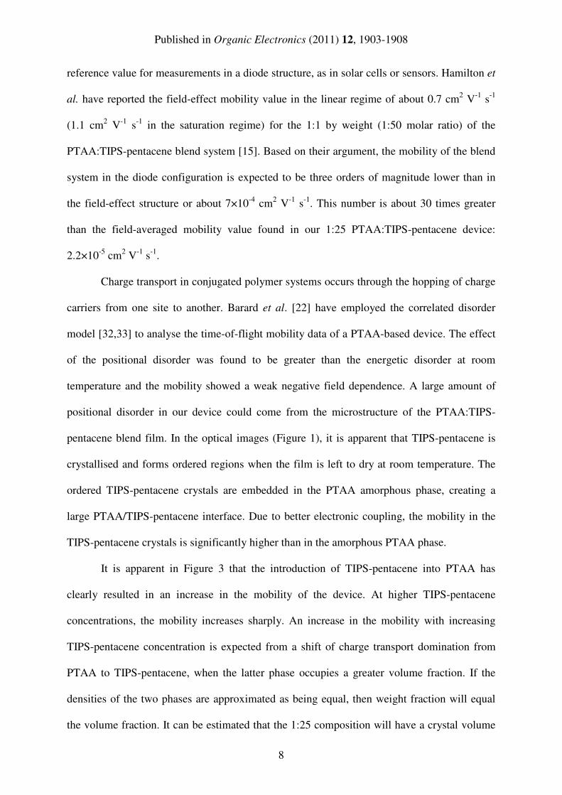
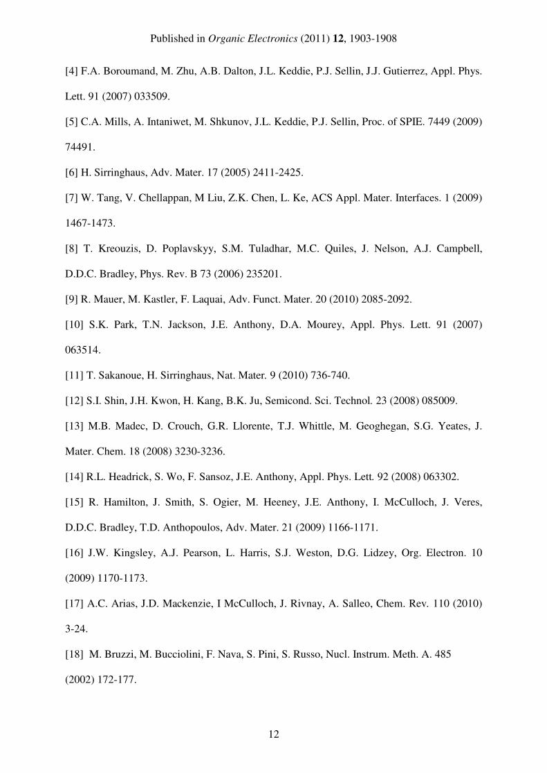
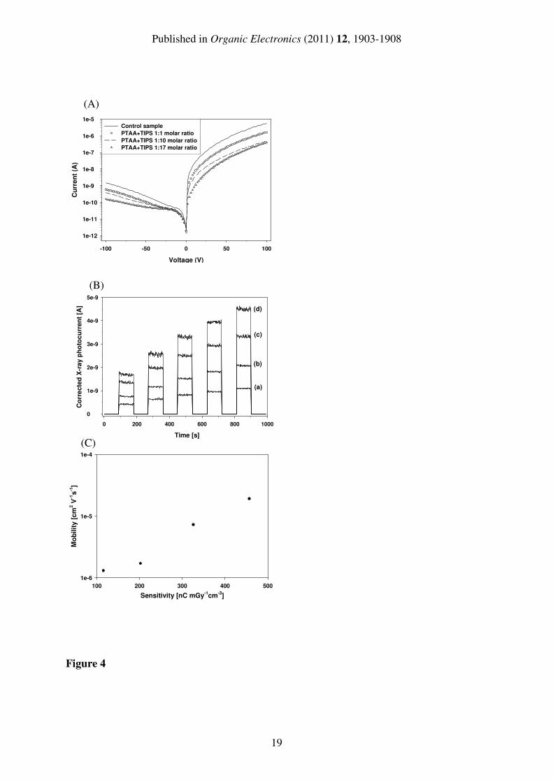
The question now arises as to how an increase in mobility in the blend will translate
into device performance. Figure 4A demonstrates the d.c. dark current-voltage characteristics
for the PTAA-based diodes containing increasing concentrations of TIPS-pentacene.
According to surface profilometry, the thickness of the active layer for every sample is
approximately 10 µm. Voltages ranging from -100 V to 100 V were applied through the ITO
back electrode. For the ITO/pristine PTAA/Al diode, the I-V curve shows a rectifying
behavior with a reverse bias leakage current density of 6.12 nA/cm2 at -100 V (field strength
of 100 kV/cm). For the devices with the blend material of PTAA and TIPS-pentacene, the I-V
characteristics still show a distinct Schottky rectification with a low leakage current in reverse
bias. The reverse bias leakage current density for the devices with 1:1, 1:10 and 1:17 by molar
ratio of PTAA:TIPS-pentacene are found to be 2.4, 1.56 and 0.6 nA/cm2 at -100 V,
respectively.
For device applications, experiments on X-ray sensors were conducted in which diode
devices were irradiated through an Al top contact by an X-ray beam. The induced
photocurrent was measured as a function of the dose rate to evaluate the performance of the
sensor. Figures 4B demonstrates dynamic photocurrent responses for devices biased at 40 V
which have an active layer made of PTAA-doped with different concentrations of TIPS-
pentacene. The dose rate was systematically increased from 13 to 66 milliGray per second
(mGy/s) in increments of 13 mGy/s. The induced photocurrent from the sensors increases
proportionally to the increasing of the X-ray dose rate, which can be attributed to a higher
Published in Organic Electronics (2011) 12, 1903-1908
10
number of generated charge carriers. The rise and fall times are both less than the sampling
rate of the instrument (<0.25 s).
The data confirm that the induced photocurrent can be significantly increased when
the active layer contains TIPS-pentacene. For all applied dose rates and operational voltages,
the X-ray photocurrent increases as the amount of TIPS-pentacene increases. For instance, at
the X-ray dose rate of 66 mGy/s, it increases from about 1.8 nA for the PTAA sensor to
approximately 9 nA for the 1:17 PTAA:TIPS-pentacene sensor, at an operational voltage of -
100 V.
The dependence of the X-ray photocurrent on the dose rate is used to define the
sensitivity. A positive correlation between the radiation sensor’s sensitivity and the charge
carrier mobility for the PTAA and the PTAA:TIPS-pentacene devices is revealed in Figure 4C.
The sensitivity of the 1:17 device is highest, and its active material has the greatest mobility
(Table 1). At the highest field strength, the sensitivity of the 1:17 device is 457 nC/mGy/cm3,
which is nearly four times that obtained for PTAA (116 nC/mGy/cm3). As TIPS-pentacene
has a relatively high charge carrier mobility, the rise in the sensitivity in the blend device can
be assigned to an increase of the ability of the active material to transport charge carriers.
However, even higher concentrations of TIPS-pentacene increase the conductivity of the
blend too much to enable its use in a rectifying diode (with a low dark current) in a sensor.
Thus, there is an upper limit to the increase in X-ray sensitivity that is possible through the
addition of TIPS-pentacene. Note that although the X-ray sensitivity of the 1:17 blend device
is below what has been reported elsewhere for tissue-equivalent diamond detectors [34],
polymers offer the distinct advantages of being lower in cost and able to coat large areas.
4. Conclusions
We have determined, for the first time, the influence of TIPS-pentacene on charge
transport in PTAA/TIPS-pentacene blends using a time-of-flight technique. Our results have
Published in Organic Electronics (2011) 12, 1903-1908
11
demonstrated that the mobility of the device increases with an increasing amount of TIPS-
pentacene The value of mobility was found to be 2.2×10⁻⁵
cm2 V
-1 s
-1, averaged for field
strengths between 3×10⁴ and 4×10
5 V cm
-1 for the 1:25 PTAA:TIPS-pentacene blend, which
is about 17 times higher than in PTAA over the same range of field strengths. Increasing
mobility correlates very well with a four-fold increase in the X-ray detection sensitivity in the
PTAA:TIPS-pentacene devices. The blend material presents the highest sensitivities reported
to-date for organic, tissue-equivalent direct radiation sensors. The higher sensitivity and
charge-carrier mobility are attributed to TIPS-pentacene crystals that provide a fast path for
charge transport. The organic blends offer the potential for processing mechanically-flexible,
large-area sensors for use in radiation protection and imaging applications. These diode
structures also offer attractive properties for other applications, including light-emitting
diodes, solar cells, and light sensors.
Acknowledgement
AI acknowledges a scholarship from the Office of the Higher Education Commission, the
Royal Thai Government. Dr. Heiko Thiem (Evonik Degussa GmbH, Germany) kindly
supplied the PTAA. The authors thank Dr. Veeramani Perumal, John-William Brown, Gary
Strudwick, Violeta Dukova and John Dear (Department of Physics, University of Surrey) for
help with sample preparation and characterization. We are very grateful to helpful comments
from T. Kreouzis (Queen Mary University) and from an anonymous reviewer.
References
[1] O.D. Jurchescu, M. Popinciuc, B.J. van Wees, T.T.M. Palstra, Adv. Mater. 19 (2007)
688-692.
[2] S.R. Forrest, Nature 428 (2004) 911-918.
[3] S. Günes, H. Neugebauer, N.S. Sariciftci, Chem. Rev. 107 (2007) 1324-1338.
Published in Organic Electronics (2011) 12, 1903-1908
12
[4] F.A. Boroumand, M. Zhu, A.B. Dalton, J.L. Keddie, P.J. Sellin, J.J. Gutierrez, Appl. Phys.
Lett. 91 (2007) 033509.
[5] C.A. Mills, A. Intaniwet, M. Shkunov, J.L. Keddie, P.J. Sellin, Proc. of SPIE. 7449 (2009)
74491.
[6] H. Sirringhaus, Adv. Mater. 17 (2005) 2411-2425.
[7] W. Tang, V. Chellappan, M Liu, Z.K. Chen, L. Ke, ACS Appl. Mater. Interfaces. 1 (2009)
1467-1473.
[8] T. Kreouzis, D. Poplavskyy, S.M. Tuladhar, M.C. Quiles, J. Nelson, A.J. Campbell,
D.D.C. Bradley, Phys. Rev. B 73 (2006) 235201.
[9] R. Mauer, M. Kastler, F. Laquai, Adv. Funct. Mater. 20 (2010) 2085-2092.
[10] S.K. Park, T.N. Jackson, J.E. Anthony, D.A. Mourey, Appl. Phys. Lett. 91 (2007)
063514.
[11] T. Sakanoue, H. Sirringhaus, Nat. Mater. 9 (2010) 736-740.
[12] S.I. Shin, J.H. Kwon, H. Kang, B.K. Ju, Semicond. Sci. Technol. 23 (2008) 085009.
[13] M.B. Madec, D. Crouch, G.R. Llorente, T.J. Whittle, M. Geoghegan, S.G. Yeates, J.
Mater. Chem. 18 (2008) 3230-3236.
[14] R.L. Headrick, S. Wo, F. Sansoz, J.E. Anthony, Appl. Phys. Lett. 92 (2008) 063302.
[15] R. Hamilton, J. Smith, S. Ogier, M. Heeney, J.E. Anthony, I. McCulloch, J. Veres,
D.D.C. Bradley, T.D. Anthopoulos, Adv. Mater. 21 (2009) 1166-1171.
[16] J.W. Kingsley, A.J. Pearson, L. Harris, S.J. Weston, D.G. Lidzey, Org. Electron. 10
(2009) 1170-1173.
[17] A.C. Arias, J.D. Mackenzie, I McCulloch, J. Rivnay, A. Salleo, Chem. Rev. 110 (2010)
3-24.
[18] M. Bruzzi, M. Bucciolini, F. Nava, S. Pini, S. Russo, Nucl. Instrum. Meth. A. 485
(2002) 172-177.
Published in Organic Electronics (2011) 12, 1903-1908
13
[19] A. Intaniwet, C.A. Mills, M. Shkunov, H. Thiem, J.L. Keddie, P.J. Sellin, J. Appl. Phys.
106 (2009) 064513.
[20] A. Intaniwet, C.A. Mills, P.J. Sellin, M. Shkunov, J.L. Keddie, ACS Appl. Mater .
Interfaces. 2 (2010) 1692-1699.
[21] J. Chen, J. Anthony, D.C. Martin, J. Phys. Chem. B 110 (2006) 16397-16403.
[22] S. Barard, M. Heeney, L. Chen, M. Cölle, M. Shkunov, I. McCulloch, N. Stingelin, M.
Philips, T. Kreouzis, J. Appl. Phys. 105 (2009) 013701.
[23] S.A. Choulis, Y. Kim, J. Nelson, D.D.C. Bradley, M. Giles, M. Shkunov, I. McCulloch,
Appl. Phys. Lett. 85 (2004) 3890-3892.
[24] Q. Shi, Y. Hou, H. Jin, Y. Li, J. Appl. Phys. 102 (2007) 073108.
[25] H. Scher, E.W. Montroll, Phys. Rev. B. 12 (1975) 2455-2477.
[26] Y. Shirota, H. Kageyama, Chem. Rev. 107 (2007) 953-1010.
[27] R. Pacios, J. Nelson, D.D.C. Bradley, C.J. Brabec, Appl. Phys. Lett. 83 (2007) 4764.
[28] A.M. Ballantyne, L. Chen, J. Dane, T. Hammant, F.M. Braun, M. Heeney, W. Duffy, I.
McCulloch, D.D.C. Bradley, J. Nelson, Adv. Funct. Mater. 18 (2008) 2373-2380.
[29] C. Tanase, E.J. Meijer, P.W.M. Blom, D.M. de Leeuw, Phy. Rev. Lett. 91 (2003) 216601.
[30] Z. Bao, A. Dodabalapur, A.J. Lovinger, Appl. Phys. Lett. 69 (1996) 4108.
[31] H. Sirringhaus, N. Tessler, R.H. Friend, Science 280 (1998) 1741-1744.
[32] S.V. Novikov, D.H. Dunlap, V.M. Kenkre, P.E. Parris, A.V. Vannikov, Phys. Rev. Lett.
81 (1998) 4472-4475.
[33] V. Coropceanu, J. Cornil, D.A.D.S. Filho, Y. Olivier, R. Silbey, J.L. Brédas, Chem. Rev.
107 (2007) 926-952.
[34] A. Lohstroh, P.J. Sellin, F. Boroumand, J. Morse, Phys. Stat. Sol. (a) 204 (2007) 3011-
3016.
Published in Organic Electronics (2011) 12, 1903-1908
14
Table 1. Charge-carrier mobility and X-ray sensitivity of PTAA and TIPS/PTAA Diodes
Composition of active
material
Charge-carrier mobility
(10-6
cm2 V
-1 s
-1)
X-ray sensitivity
(nC mGy-1
cm-3
)
PTAA 1.3 116
TIPS:PTAA = 17:1 19 457
Published in Organic Electronics (2011) 12, 1903-1908
15
Figure Captions
Figure 1. Polarized optical images of PTAA blended with TIPS-pentacene in molar ratios of
(A) 1:1, (B) 1:10 and (C) 1:17. The long axis of the crystals lies in the plane of the film.
Scale bar is 100 µm.
Figure 2 (A) Transient photocurrent for hole transport in the PTAA blended with TIPS-
pentacene of 1:17 by molar ratio at (a) 160 V, and (b) 260 V. The inset shows a double
logarithmic plot at these two applied voltages. (B) Plots of the inverse effective lifetime, τ, as
a function of the applied voltage over the square of the film thickness for pure PTAA (), and
PTAA blended with TIPS-pentacene in molar ratios of 1:1 (), 1:10 (∆), 1:17 () and 1:25 ().
Figure 3 Hole mobility as a function of TIPS-pentacene concentration in mole %. The
average mobility values for field strengths, ranging from 3×10⁴ to 4×10
5 V cm
-1, are reported
here.
Figure 4 (A) Semi-log current-voltage characteristics for the ITO/PTAA-based active
layer/Al diodes when active layers are pure PTAA (solid line), PTAA blended with TIPS-
pentacene of 1:1(), 1:10 (dashed line), and 1:17 (∆) by molar ratio. (B) Dynamic X-ray
photocurrent for the ITO/PTAA-based/Al sensors with an active layer (10 µm thick) of (a)
pure PTAA, and PTAA blended with TIPS-pentacene of in molar ratios of (b) 1:1, (c) 1:10,
and (d) 1:17, when operated at 40 V. The devices were irradiated by 17.5 keV X-rays through
an Al top contact with increasing dose rate from left to right: 13, 27, 40, 54 and 66 mGy s-1
.
(C) Positive correlation between the X-ray sensitivity of the sensors and the charge-carrier
mobility of their active material (PTAA or PTAA/TIPS-pentacene blend).
Published in Organic Electronics (2011) 12, 1903-1908
16
Figure 1
(A)
(A)
(B)
(C)
Published in Organic Electronics (2011) 12, 1903-1908
17
V/d2 (V/cm
2)
0.0 2.0e+8 4.0e+8 6.0e+8 8.0e+8 1.0e+9 1.2e+9
1/ ττ ττ
(s
-1)
0
1000
2000
3000
4000
5000
6000Pure PTAA
PTAA:TIPS 1:1 molar ratio
PTAA:TIPS 1:10 molar ratio
PTAA:TIPS 1:17 molar ratio
PTAA:TIPS 1:25 molar ratio
Figure 2
Time [µµµµs]
0 1000 2000 3000 4000 5000
Ph
oto
cu
rren
t d
en
sit
y [
A c
m-2
]
0
20
40
60
80
100
log (time [µµµµs])
1.5 2.0 2.5 3.0 3.5 4.0
log
(p
ho
toc
urr
en
t d
en
sit
y [
A c
m-2
])
0.4
0.8
1.2
1.6
2.0
(a)
(b)
ττττ(a)
(b)
(A)
(B)
Published in Organic Electronics (2011) 12, 1903-1908
18
TIPS-pentacene [mole %]
0 20 40 60 80 100
Mo
bil
ity [
cm
2 V
-1 s
-1]
0.0
1.0e-5
2.0e-5
3.0e-5
Pure PTAA 1:1 molar ratio
1:10 molar ratio
1:17 molar ratio
1:25 molar ratio
Figure 3
Published in Organic Electronics (2011) 12, 1903-1908
19
Sensitivity [nC mGy-1
cm-3
]
100 200 300 400 500
Mo
bil
ity [
cm
2 V
-1s
-1]
1e-6
1e-5
1e-4
Figure 4
Time [s]
0 200 400 600 800 1000
Co
rre
cte
d X
-ra
y p
ho
toc
urr
en
t [A
]
0
1e-9
2e-9
3e-9
4e-9
5e-9
(a)
(b)
(c)
(d)
(B)
Voltage (V)
-100 -50 0 50 100
Cu
rre
nt
(A)
1e-12
1e-11
1e-10
1e-9
1e-8
1e-7
1e-6
1e-5Control sample
PTAA+TIPS 1:1 molar ratio
PTAA+TIPS 1:10 molar ratio
PTAA+TIPS 1:17 molar ratio
(A)
(C)