Embed Size (px)
Citation preview
High-efficiency organic light-emitting diodes based on the gradient doping andnonlinear cross-fading doping in transporting layers
Jing Wang (SID Student Member) Abstract — We have de
Saijun HuangJun Liu (SID Student Member)
Xinkai Wu (SID Student Member)
Xindong Shi (SID Student Member)Chaoping Chen (SID Member)
Zhicheng Ye (SID Member)
Jiangang Lu (SID Member)Yikai Su (SID Member)
Gufeng He (SID Member)
monstrated that carrier injection and transporting can be fine-tuned via gradientp-doping and n-doping in organic light-emitting diodes. The doping profile of gradient doping intransporting layer is ultrahigh at the electrode side, declining gradually with the depth into the deviceuntil the emission layer. This not only ensures perfect charge injection from electrode to organictransporting layer but also proves an efficient charge transport for light emission. It is proposed thatlow doping ratio close to the emission layer may avoid possible quenching of excitons by the diffusionof dopant as well. A device based on gradient doping has been proved to obtain better carrier injectionand achieve higher external quantum efficiency. To get smoother charge injection and transporting, and
simplify the fabrication process, we have developed a nonlinear cross-fading doping in transportinglayer, which has been demonstrated to further enhance the current density characteristics.
Received 07/25/13; accepted 03/16/14.The authors are with National Engineering Lab for TFShanghai 200240, China; e-mail: [email protected]© Copyright 2014 Society for Information Display 1
Keywords — organic light emitting, injection, transporting, gradient doping, cross-fading doping.
DOI # 10.1002/jsid.215
1 Introduction
Organic light-emitting diodes (OLEDs) have attracted exten-sive research interests over the last two decades and have em-braced the mass production. Despite numerous advantages,OLEDs still have some issues to be overcome to obtain lowervoltage, higher luminance and efficiency, and better stability.Charge carrier injection and transporting are two importantprocesses for light emission. However, because of large en-ergy barrier between electrode and transporting layer, chargecarriers are difficult to be injected into the organic layers,which results in high operating voltage and low efficiency.To solve this problem, an injection layer between electrodeand transporting layer and doped transporting layer havebeen introduced.1–3
The injection layer reduces the energy barrier greatly dueto the generation of a thin dipole layer.4 But the mobility ofundoped transporting layer is relatively low; therefore, thevoltage drop over thick transporting layer is still large,resulting in high operating voltage. On the other hand, dopingappropriate dopant material into transporting layer will gener-ate additional charge carriers, and these carriers can almostmove freely, resulting increased conductivity. Such conductiv-ity increase can be up to several orders, and the voltage dropover such doped layer is negligible. Furthermore, for thedoped transporting layer, a much stronger band bending oc-curs, and the space charge layer is very thin, which makesthe charge carrier injection much easier via tunneling.5
T-LCDMaterials and Technou.cn.071-0922/14/2201-0215$1.0
However, the doping ratio is usually quite low; there is notenough energy barrier reduce caused by the dipole layer atthe interface of electrode and transporting layer.4
To further reduce the operating voltage, we proposed agradient doping profile in the transporting layer, where thedoping concentration adjacent to the electrode is very highto ensure perfect charge injection, and the concentration de-crease gradually with the depth into the device until the emis-sion layer. The medium doping concentration in the middleof the transporting layer still keeps its conductivity at a highlevel. The low concentration close to the emission layer mayavoid the possible quenching of the excitons by the diffusionof dopants. Our results prove that the gradient doping leadsto the best power efficiency and external quantum efficiency(EQE). To simplify the process of the gradient doping and di-minish the interfacial effects, a nonlinear cross-fading dopingis proposed as well. The profile of the cross-fading doping isnonlinear with continuous decrease from ultrahigh at theelectrode side to ultralow at the emission layer side. It hasbeen demonstrated that nonlinear cross-fading doping intransporting layer can further enhance the current densitycharacteristics.
2 Experimental
Patterned indium–tin–oxide (ITO) substrates are preparedand precleaned by a multistep solvent process before
logies, Department of Electronic Engineering,Shanghai Jiao Tong University,
0.
Journal of the SID 22/01, 2014 83
transporting to vacuum thermal evaporator. In this study,[N-(1-naphthyl)-N-phenyl-amino] biphenyl (NPB) is used as ahole transporting material and 2,3,5,6-tetrafluoro-7,7,8,8-tetracyanoquinodimethane (F4-TCNQ) is the correspondingp-type dopant. High electron mobility (~10�3 cm2/V·s)transporting material VOM1973 is used as electron trans-porting layer (ETL), and its corresponding n-type dopant is8-hydroxyquinolinolato-lithium (Liq). All devices are fabri-cated under a base pressure of 5 × 10�6 Torr without breakingthe vacuum. The organic materials, except for the dopants,are evaporated at a rate of 0.5 ~ 1 Å/s. At the end, 100-nm-thick aluminum is deposited as the cathode. The active areadefined by the overlap of the ITO anode and the Al cathodeis 3mm× 3mm. The current density–voltage–luminancecharacteristics of the devices are measured using acomputer-controlled Keithley 2400 and Topcon BM-7A mea-surement system. All the measurements are carried out atroom temperature under ambient atmosphere.6
3 Gradient doping in electron transporting layer
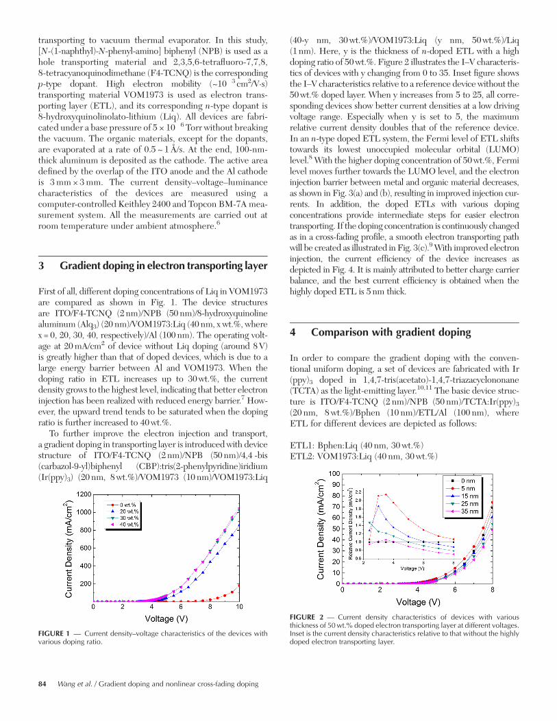
First of all, different doping concentrations of Liq in VOM1973are compared as shown in Fig. 1. The device structuresare ITO/F4-TCNQ (2nm)/NPB (50 nm)/8-hydroxyquinolinealuminum (Alq3) (20 nm)/VOM1973:Liq (40 nm, x wt.%, wherex = 0, 20, 30, 40, respectively)/Al (100 nm). The operating volt-age at 20mA/cm2 of device without Liq doping (around 8V)is greatly higher than that of doped devices, which is due to alarge energy barrier between Al and VOM1973. When thedoping ratio in ETL increases up to 30wt.%, the currentdensity grows to the highest level, indicating that better electroninjection has been realized with reduced energy barrier.7 How-ever, the upward trend tends to be saturated when the dopingratio is further increased to 40wt.%.
To further improve the electron injection and transport,a gradient doping in transporting layer is introduced with devicestructure of ITO/F4-TCNQ (2nm)/NPB (50 nm)/4,4 -bis(carbazol-9-yl)biphenyl (CBP):tris(2-phenylpyridine)iridium(Ir(ppy)3) (20 nm, 8wt.%)/VOM1973 (10 nm)/VOM1973:Liq
FIGURE 1 — Current density–voltage characteristics of the devices withvarious doping ratio.
84 Wang et al. / Gradient doping and nonlinear cross-fading doping
(40-y nm, 30wt.%)/VOM1973:Liq (y nm, 50wt.%)/Liq(1 nm). Here, y is the thickness of n-doped ETL with a highdoping ratio of 50wt.%. Figure 2 illustrates the I–V characteris-tics of devices with y changing from 0 to 35. Inset figure showsthe I–V characteristics relative to a reference device without the50wt.% doped layer. When y increases from 5 to 25, all corre-sponding devices show better current densities at a low drivingvoltage range. Especially when y is set to 5, the maximumrelative current density doubles that of the reference device.In an n-type doped ETL system, the Fermi level of ETL shiftstowards its lowest unoccupied molecular orbital (LUMO)level.8 With the higher doping concentration of 50wt.%, Fermilevel moves further towards the LUMO level, and the electroninjection barrier between metal and organic material decreases,as shown in Fig. 3(a) and (b), resulting in improved injection cur-rents. In addition, the doped ETLs with various dopingconcentrations provide intermediate steps for easier electrontransporting. If the doping concentration is continuously changedas in a cross-fading profile, a smooth electron transporting pathwill be created as illustrated in Fig. 3(c).9With improved electroninjection, the current efficiency of the device increases asdepicted in Fig. 4. It is mainly attributed to better charge carrierbalance, and the best current efficiency is obtained when thehighly doped ETL is 5 nm thick.
4 Comparison with gradient doping
In order to compare the gradient doping with the conven-tional uniform doping, a set of devices are fabricated with Ir(ppy)3 doped in 1,4,7-tris(acetato)-1,4,7-triazacyclononane(TCTA) as the light-emitting layer.10,11 The basic device struc-ture is ITO/F4-TCNQ (2 nm)/NPB (50 nm)/TCTA:Ir(ppy)3(20 nm, 8wt.%)/Bphen (10 nm)/ETL/Al (100 nm), whereETL for different devices are depicted as follows:
ETL1: Bphen:Liq (40 nm, 30wt.%)ETL2: VOM1973:Liq (40 nm, 30wt.%)
FIGURE 2 — Current density characteristics of devices with variousthickness of 50wt.% doped electron transporting layer at different voltages.Inset is the current density characteristics relative to that without the highlydoped electron transporting layer.
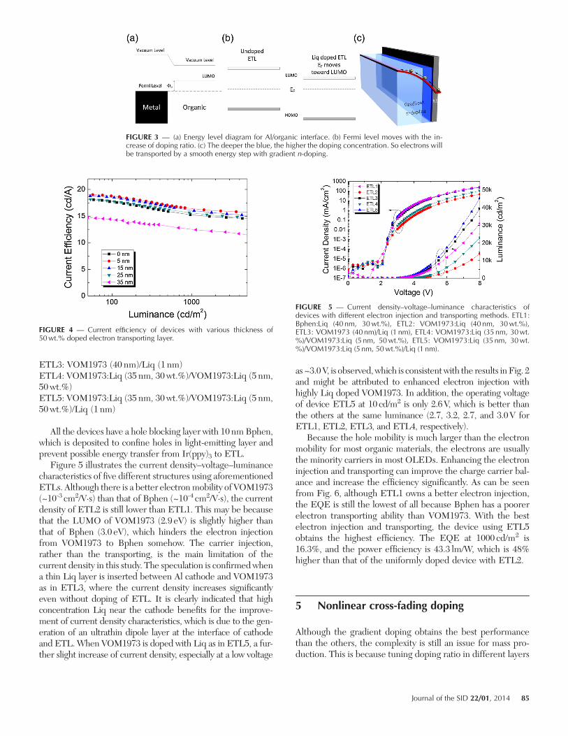
FIGURE 3 — (a) Energy level diagram for Al/organic interface. (b) Fermi level moves with the in-crease of doping ratio. (c) The deeper the blue, the higher the doping concentration. So electrons willbe transported by a smooth energy step with gradient n-doping.
FIGURE 4 — Current efficiency of devices with various thickness of50wt.% doped electron transporting layer.
FIGURE 5 — Current density–voltage–luminance characteristics ofdevices with different electron injection and transporting methods. ETL1:Bphen:Liq (40 nm, 30wt.%), ETL2: VOM1973:Liq (40 nm, 30wt.%),ETL3: VOM1973 (40nm)/Liq (1 nm), ETL4: VOM1973:Liq (35 nm, 30wt.%)/VOM1973:Liq (5 nm, 50wt.%), ETL5: VOM1973:Liq (35 nm, 30wt.%)/VOM1973:Liq (5 nm, 50wt.%)/Liq (1 nm).
ETL3: VOM1973 (40 nm)/Liq (1 nm)ETL4: VOM1973:Liq (35 nm, 30wt.%)/VOM1973:Liq (5 nm,50wt.%)ETL5: VOM1973:Liq (35 nm, 30wt.%)/VOM1973:Liq (5 nm,50wt.%)/Liq (1 nm)
All the devices have a hole blocking layer with 10nm Bphen,which is deposited to confine holes in light-emitting layer andprevent possible energy transfer from Ir(ppy)3 to ETL.
Figure 5 illustrates the current density–voltage–luminancecharacteristics of five different structures using aforementionedETLs. Although there is a better electronmobility of VOM1973(~10-3 cm2/V·s) than that of Bphen (~10-4 cm2/V·s), the currentdensity of ETL2 is still lower than ETL1. This may be becausethat the LUMO of VOM1973 (2.9 eV) is slightly higher thanthat of Bphen (3.0 eV), which hinders the electron injectionfrom VOM1973 to Bphen somehow. The carrier injection,rather than the transporting, is the main limitation of thecurrent density in this study. The speculation is confirmed whena thin Liq layer is inserted between Al cathode and VOM1973as in ETL3, where the current density increases significantlyeven without doping of ETL. It is clearly indicated that highconcentration Liq near the cathode benefits for the improve-ment of current density characteristics, which is due to the gen-eration of an ultrathin dipole layer at the interface of cathodeand ETL.When VOM1973 is doped with Liq as in ETL5, a fur-ther slight increase of current density, especially at a low voltage
as ~3.0V, is observed, which is consistent with the results in Fig. 2and might be attributed to enhanced electron injection withhighly Liq doped VOM1973. In addition, the operating voltageof device ETL5 at 10 cd/m2 is only 2.6V, which is better thanthe others at the same luminance (2.7, 3.2, 2.7, and 3.0V forETL1, ETL2, ETL3, and ETL4, respectively).
Because the hole mobility is much larger than the electronmobility for most organic materials, the electrons are usuallythe minority carriers in most OLEDs. Enhancing the electroninjection and transporting can improve the charge carrier bal-ance and increase the efficiency significantly. As can be seenfrom Fig. 6, although ETL1 owns a better electron injection,the EQE is still the lowest of all because Bphen has a poorerelectron transporting ability than VOM1973. With the bestelectron injection and transporting, the device using ETL5obtains the highest efficiency. The EQE at 1000 cd/m2 is16.3%, and the power efficiency is 43.3 lm/W, which is 48%higher than that of the uniformly doped device with ETL2.
5 Nonlinear cross-fading doping
Although the gradient doping obtains the best performancethan the others, the complexity is still an issue for mass pro-duction. This is because tuning doping ratio in different layers
Journal of the SID 22/01, 2014 85
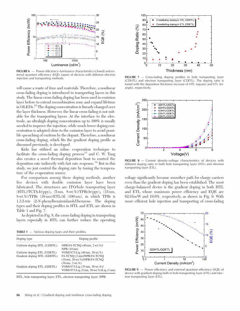
FIGURE 6 — Power efficiency–luminance characteristics (closed) and ex-ternal quantum efficiency (EQE) (open) of devices with different electroninjection and transporting methods. FIGURE 7 — Cross-fading doping profiles in hole transporting layer
(CDHTL) and electron transporting layer (CDETL). The doping ratio istuned with the deposition thickness increase of HTL (square) and ETL (tri-angle), respectively.
FIGURE 8 — Current density–voltage characteristics of devices withdifferent doping ratio in both hole transporting layer (HTL) and electrontransporting layer (ETL).
will cause a waste of time and materials. Therefore, a nonlinearcross-fading doping is introduced in transporting layers in thisstudy. The linear cross-fading doping has been used in emissionlayer before to extend recombination zone and expand lifetimein OLEDs.12 The doping concentration is linearly changed overthe layer thickness. However, the linear cross-fading is not suit-able for the transporting layers. At the interface to the elec-trode, an ultrahigh doping concentration up to 100% is usuallyneeded to improve the injection, while much lower doping con-centration is adopted close to the emission layer to avoid possi-ble quenching of excitons by the dopant. Therefore, a nonlinearcross-fading doping, which fits the gradient doping profile asdiscussed previously, is developed.
Kido has utilized an inline evaporation technique tofacilitate the cross-fading doping process13 and C. W. Tangalso creates a novel thermal deposition boat to control thedeposition rate indirectly with fast rate response.14 But in thisstudy, we just control the doping rate by tuning the tempera-ture of the evaporation source.
For comparison among these doping methods, anotherfive devices with double emission layer have beenfabricated. The structures are ITO/hole transporting layer(HTL)/TCTA:Ir(ppy)3 (5 nm, 8wt.%)/TPBi:Ir(ppy)3 (15 nm,8wt.%)/TPBi (10 nm)/ETL/Al (100nm), in which TPBi is1,3,5-tris (2-N-phenylbenzimidazolyl)benzene. The dopingtypes and their doping profiles in HTL and ETL are shown inTable 1 and Fig. 7.
As depicted in Fig. 8, the cross-fading doping in transportinglayers especially in HTL can further reduce the operating
TABLE 1 — Various doping types and their profiles.
Doping type Doping profile
Uniform doping HTL (UDHTL) NPB:F4-TCNQ (40 nm, 2wt.%)/NPB (10 nm)
Uniform doping ETL (UDETL) VOM1973:Liq (40 nm, 30wt.%)Gradient doping HTL (GDHTL) F4-TCNQ (2 nm)/NPB:F4-TCNQ
(10 nm, 20wt.%)/NPB:F4-TCNQ(30 nm, 2wt.%)
Gradient doping ETL (GDETL) VOM1973:Liq (35 nm, 30wt.%)/VOM1973:Liq (5 nm, 50wt.%)/Liq (1 nm)
HTL, hole transporting layer; ETL, electron transporting layer; NPB.
86 Wang et al. / Gradient doping and nonlinear cross-fading doping
voltage significantly because smoother path for charge carrierseven than the gradient doping has been established. The mostcharge-balanced device is the gradient doping in both HTLand ETL whose maximum power efficiency and EQE are62.9 lm/W and 19.6%, respectively, as shown in Fig. 9. Withmore efficient hole injection and transporting of cross-fading
FIGURE 9 — Power efficiency and external quantum efficiency (EQE) ofdevice with gradient doping both in hole transporting layer (HTL) and elec-tron transporting layer (ETL).
Jing Wang received his BS degree in ElectronicEngineering from Xidian University, China, in2007. Currently, he is pursuing his MS degreeunder the supervision of Prof. Gufeng He inShanghai Jiao Tong University. His research in-terests include high-efficiency organic light-emitting diodes and charge carrier injection,and transporting in organic semiconductors.
doping inHTL, the efficiency is reduced because of a bit poorercharge balance. However, this method provides a new way toimprove the carrier injection and transporting and to tune thecharge carrier balance. Moreover, by diminishing the interfacialeffects, the cross-fading doping may have better stability. Inaddition, it can also be easily achieved for mass production withnovel evaporation processes.
Saijun Huang was born in 1988. She receivedher BS degree in Information Engineering fromShanghai Jiao Tong University, China, in 2007.Currently, she is pursuing her MS degree onElectronics and Science Technology in ShanghaiJiao Tong University. Her research is focused onthe extraction efficiency of organic light-emit-ting diode.
6 Summary
We show that by using the gradient doping, 16.3% EQEis achieved for single emission layer at 1000 cd/m2 wherethe power efficiency is also increased by 47.8% comparedwith the uniform doping device. A maximum EQE of19.6% and a power efficiency of 62.9 lm/W are alsoobtained with double emission layer using the gradientdoping in HTL and ETL. Finally, an efficient and com-mercial potential nonlinear cross-fading doping intransporting layer is also proved to further increase thecarrier injection and transporting.
Jun Liu received his master’s degree from theCollege of Materials Engineering, Nanjing For-estry University, Nanjing, China, in 2010.Currently, he is a PhD student majoring inorganic light-emitting diodes (OLEDs) inNational Engineering Laboratory of TFT-LCDMaterials and Technologies, Shanghai JiaoTong University, Shanghai, China. His re-search interests include tandem OLED, solu-tion-processed optoelectronic devices, OLEDdisplay, and OLED lighting.
Xinkai Wu received his BS degree and MSdegrees in Polymer Science and Engineeringfrom the University of Science and Technol-ogy of Jiangsu from 2005 to 2012. Then, heis pursuing PhD degrees in Electronics Sci-ence and Technology from Shanghai Jiao TongUniversity. His research interests include flex-ible electrode and flexible organic light-emit-ting diode devices fabricating.
Xindong Shi was born in 1989. He receivedhis BS degrees from the College of ElectricalInformation, Hangzhou Dianzi University,Hangzhou, China, in 2012. Currently, he is amaster’s student in the Department of Elec-tronic Engineering, Shanghai Jiao Tong Uni-versity, Shanghai, China. His researchinterests are focused on top-emission organiclight-emitting diode (OLED) and lightoutcoupling for highly efficient OLED.
References1 L. S. Hung et al., “Enhanced electron injection in organic electrolumi-nescence devices using an Al/LiF electrode,” Appl. Phys. Lett. 70,152–154 (1997).
2 J. Blochwitz et al., “Low voltage organic light emitting diodes featuringdoped phthalocyanine as hole transport material,” Appl. Phys. Lett. 73,729–731 (1998).
3 G. He et al., “White stacked OLED with 38 lm/W and 100,000-hour life-time at 1000 cd/m2 for display and lighting applications,” J. Soc. Info. Dis-play 17, 159–165 (2007).
4 I.-H. Hong et al., “Effective hole injection of organic light-emitting diodesby introducing buckminsterfullerene on the indium tin oxide anode,”Appl. Phys. Lett. 87, 063502 (2005).
5 J. Blochwitz et al., “Interface electronic structure of organic semiconductorswith controlled doping levels,” Org. Electron. 2, 97–104 (2001).
6 J. Wang et al., “Enhancing the hole injection and transporting of organiclight-emitting diodes by utilizing gradient doping,” Mol. Cryst. Liq. Cryst.574, 129–134 (2013).
7 A. Kumar et al., “Effect of doping of 8-hydroxyquinolinatolithium on elec-tron transport in tris (8-hydroxyquinolinato) aluminum,” J. Appl. Phys.,109, 114511 (2011).
8 K. Walzer et al., “Highly efficient organic devices based on electricallydoped transport layers,” Chem. Rev. 107, 1233–1271 (2007).
9 T. N. Ng et al., “Dependence of charge injection on temperature, electricfield, and energetic disorder in an organic semiconductor,” Phys. Rev.Lett. 98, 066101 (2007).
10 M. Ikai et al., “Highly efficient phosphorescence from organic light-emitting devices with an exciton-block layer,” Appl. Phys. Lett. 79,156–158 (2001).
11 G. He et al., “Very high-efficiency and low voltage phosphorescentorganic light-emitting diodes based on a p-i-n junction,” J. Appl.Phys. 95, 5773 (2004).
12 F. Lindla et al., “Employing exciton transfer molecules to increase the life-time of phosphorescent red organic light emitting diodes,” Appl. Phys.Lett. 98, 173304 (2011).
13 J. Kido, “High-performance OLEDs for displays and general lighting,”SID symposium Digest 61, 931–932 (2008).
14 S. Lee and C. W. Tang, “Fabrication of a blue organic light-emittingdiode with a novel thermal deposition boat,” J. Vac. Sci. Technol. B29, 062401 (2011).
Journal of the SID 22/01, 2014 87
Chaoping Chen received his BS degree in2004 from Shanghai University and his MSand PhD degrees in 2006 and 2009, respec-tively, from Pusan National University, SouthKorea. He worked at Infovision Optoelectron-ics and Shanghai Tianma for 3 odd years be-fore he joined the faculty of Shanghai JiaoTong University as an assistant professor in2012. His research interests include hologra-phy, three-dimensional display, liquid-crystaldisplay, and solid-state lighting.
Zhicheng Ye was born in 1977. He receivedhis BS and master’s degrees from the Depart-ment of Physics, Beijing Normal Universityin 1999 and 2002, respectively, and PhD de-gree from the Institute of Semiconductors,Chinese Academy of Sciences, Beijing, China,in 2006. Currently, he is an Associate Profes-sor in Department of Electronic Engineering,Shanghai Jiao Tong University, Shanghai,China. His research interests include micro–nano fabrication and nano-optical devices, es-pecially for green displays and lighting.
Jiangang Lu received his PhD degree from theCollege of Information Science and Engineering,Zhejiang University, Hangzhou, China, in 2003.He performed research on liquid-crystal displays(LCD) with the Next-Generation LCD ResearchCenter, LCD business, Samsung Electronics, from2003 to 2009. Since 2009, he has been with theNational Engineering Laboratory of TFT-LCDMate-rials and Technologies, Shanghai Jiao Tong Univer-sity, Shanghai, China, as an Associate Professor. Hisresearch includes liquid crystal and polymer mate-rial, liquid crystal photonic device, microstructureoptic device, and three-dimensional display.
Yikai Su received his BS degree from the HefeiUniversity of Technology, China, in 1991;MS de-gree from the Beijing University of Aeronauticsand Astronautics, China, in 1994; and PhD de-gree in Electronic Engineering fromNorthwesternUniversity, Evanston, IL, USA, in 2001. Prior tojoining Shanghai Jiao Tong University in 2004,he worked at Bell Laboratories, New Jersey,USA. He is currently a Full Professor of thedepartment of Electronic Engineering. Heserves as the Chapter Chair of Institute of Elec-trical and Electronics Engineers (IEEE) PhotonicsSociety in Shanghai and a Faculty Advisor ofthe Shanghai Jiao Tong University Optical Sci-
ence of America (OSA) student chapter. His research area coversmicrophotonic and nanophotonic devices and real-time holographicthree-dimensional display. Prof. Su serves as a Topical Editor of Optics Let-ters; he was a Feature Editor of Applied Optics, a Guest Editor of IEEEJSTQE on “Nonlinear Optical Signal Processing” May/June issue of2008. He also served as TPC cochairs/members for a large number of in-ternational conference. Prof. Su is a senior member of IEEE and a memberof Optical Science of America and The Society for Information Display(SID). Prof. Su serves as the Director of the Center for Opto/Electronic Ma-terials and Devices and Vice Director of National Engineering Lab for TFT-LCD Materials and Technologies.
Gufeng He received his BS degree in PolymerScience and Engineering from the University ofScience and Technology of China. Then, hestudied organic optoelectronic devices at theInstitute of Chemistry, Chinese Academy of Sci-ences, and obtained his MS and PhD degrees.From 2002 to 2005, he performed postdoctoralresearch on high-performance organic light-emitting devices at the University of Technol-ogy at Dresden, Germany. Thereafter, heworked at Novaled AG as a Senior Scientistfor 5 years on high-efficiency and long-lifetimewhite organic light-emitting device develop-ment for display and lighting applications. In
2010, he became a Professor at Shanghai Jiao Tong University in China.His main research interests are organic optoelectronic functional mate-rials and devices.
88 Wang et al. / Gradient doping and nonlinear cross-fading doping