Embed Size (px)
Citation preview
ELECTRON DYNAMICS DIVISION
FINAL REPORT
HIGH EFFICIENCY
TRAVELING WAVE TUBE
DEVELOPMENT
FOR
SPACE COMMUNICATIONS
PREPARED FOR
NATIONAL AERONAUTICS AND SPACE ADMINISTRATIONLEWIS RESEARCH CENTER21000 BROOKPARK ROAD
CLEVELAND, OH 44135
CONTRACT NO. NAS 3-24897
™ HIGH-EFFICIENCY 20 GHz N92-19191ING WAVE TUBE DEVELOPMENT FOR SPACE
COMMUNICATIONS Final Report (HughesAircraft Co.) 93 p CSCL 09A
G3/32 0061506
https://ntrs.nasa.gov/search.jsp?R=19920009949 2018-05-25T07:50:10+00:00Z
FINAL REPORT
HIGH EFFICIENCY 20 GHz
TRAVELING WAVE TUBE DEVELOPMENT
FOR
SPACE COMMUNICATIONS
PREPARED FOR
NATIONAL AERONAUTICS AND SPACE ADMINISTRATIONLEWIS RESEARCH CENTER21000 BROOKPARK ROAD
CLEVELAND, OH 44135
NASACR-187160CONTRACT NO. MAS 3-24897
OCTOBER 1991
HUGHES AIRCRAFT COMPANYELECTRON DYNAMICS DIVISION3100 WEST LOMITA BOULEVARD
P.O. BOX 2999TORRANCE, CA 90509-2999
TABLE OF CONTENTS
Section Page
1.0 PROGRAM OVERVIEW 1-1
1.1 Introduction 1-11.2 Program Goals 1-11.3 Program Accomplishments 1-1
2.0 DIAMOND ROD TECHNOLOGY 2-1
2.1 Introduction 2-12.2 Past Experience 2-12.3 New Methods 2-42.4 Circuit Thermal Tester 2-62.5 Diamond Circuit Mechanical Analysis 2-82.6 Loss Patterns Using TiC Sputtering 2-9
3.0 TWT DESIGN 3-1
3.1 Design Approach 3-13.2 RF Circuit Design 3-23.3 Velocity Tapered Helix 3-3
3.3.1 Comparison Between Computed and Measured DVTDesigns 3-4
3.4 Multistage Graphite Collector 3-123.5 Electron Gun . 3-133.6 PPM Design 3-16
4.0 TWT CONFIGURATION 4-1
4.1 Introduction 4-14.2 Configuration by Serial Number 4-1
5.0 TWT Test Results 5-1
5.1 Serial Number 1 5-15.2 Serial Number 2 5-35.3 Serial Number 3 5-5
6.0 CONCLUSIONS AND RECOMMENDATIONS 6-1
6.1 Conclusions 6-16.2 Recommendations 6-1
Appendix
A 935H Traveling-Wave Tube Diamond Circuit Mechanical Analysis A-l
iii
PRECEDING PAGE BLANK NOT FILMED
LIST OF ILLUSTRATIONS
Figure Page
2-1 Normalized phase velocity curves comparing helices supported by 0.005"wide diamond and 0.020" wide beryllia. 2-2
2-2 Circuit cold loss measurements on the diamond and beryllia supportedhelix circuits. 2-3
2-3 Diamond supported helix assembly using old fabrication technique. 2-3
2-4 Diamond supported helix assembly using new fabrication technique. 2-5
2-5 Cross section of diamond supported helix assembly. 2-5
2-6 Thermal test configuration. 2-7
2-7 Helix temperature comparison. 2-8
2-8 Finite element model of the 953H circuit assembly. 2-9
2-9 Attenuation mask. 2-10
2-10 Improved attenuation mask. 2-11
2-11 Welding instructions. 2-12
3-1 Cross-section of the 953H input circuit assembly. 3-3
3-2 Cross-section of the 953H output circuit assembly. 3-4
3-3 953H helix pitch profiles. 3-5
3-4 953H input circuit loss patterns. 3-6
3-5 953H output circuit loss patterns. 3-7
3-6 953H BB3 final design/efficiency versus clean length. 3-10
3-7 953H SN3/clean length versus BWO starting current. 3-11
3-8 Helix to barrel thermal path. 3-11
3-9 Cross section of a four-stage POCO collector. 3-12
3-10 Electron trajectories in the collector region for the 953H using a DVTcircuit. 3-14
vPRECEDING PAGI BLANK NOT FUMED
LIST OF ILLUSTRATIONS (CONTINUED)
Figure Page
3-11 953H gun thermal beam profile. 3-16
3-12 Electron trajectories from the cathode into the PPM focusing field regionfor the 953H TWT. 3-17
3-13 Peak magnetic field and flux density versus magnet outer diameter. 3-18
4-1 953H TWT final vacuum assembly. 4-2
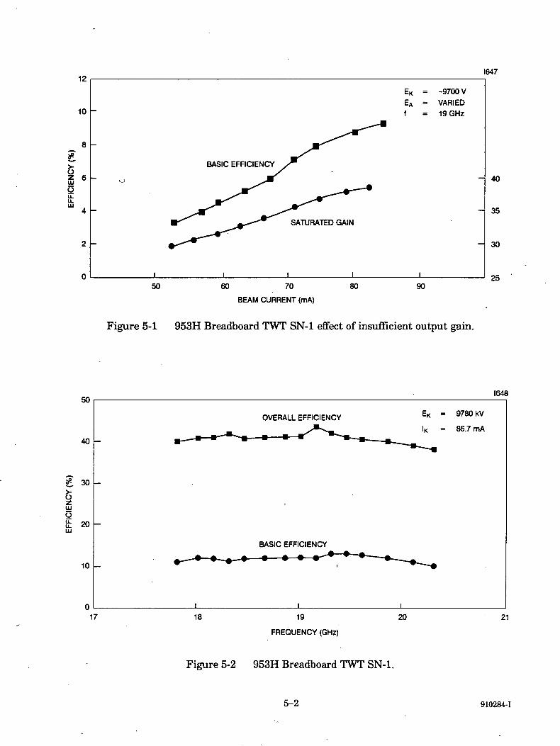
5-1 953H Breadboard TWT SN-1 effect of insufficient output gain. 5-2
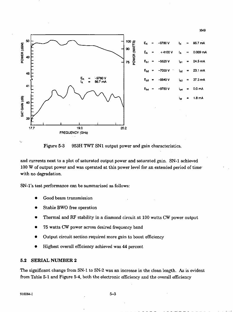
5-2 953H Breadboard TWT SN-1. 5-2
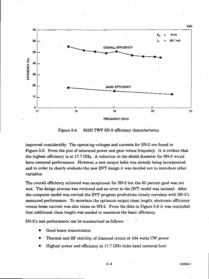
5-3 953H TWT SN1 output power and gain characteristics. 5-3
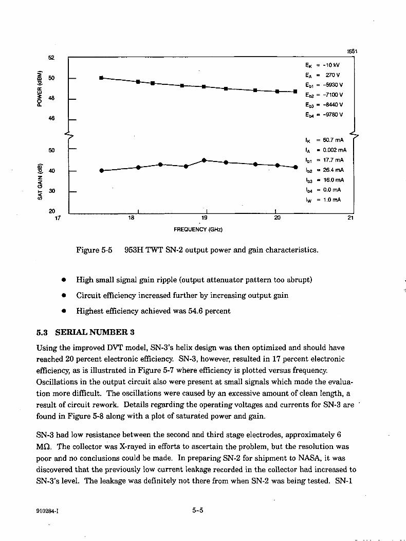
5-4 953H TWT SN-2 efficiency characteristics. 5-4
5-5 953H TWT SN-2 output power and gain characteristics. 5-5
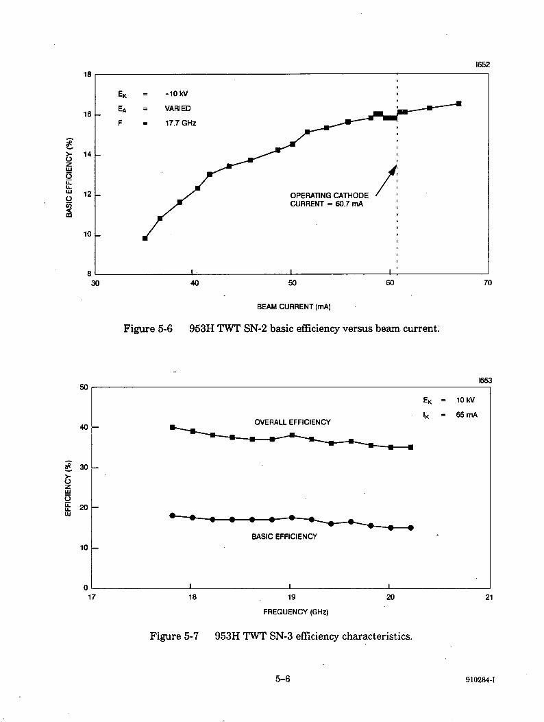
5-6 953H TWT SN-2 basic efficiency versus beam current. 5-6
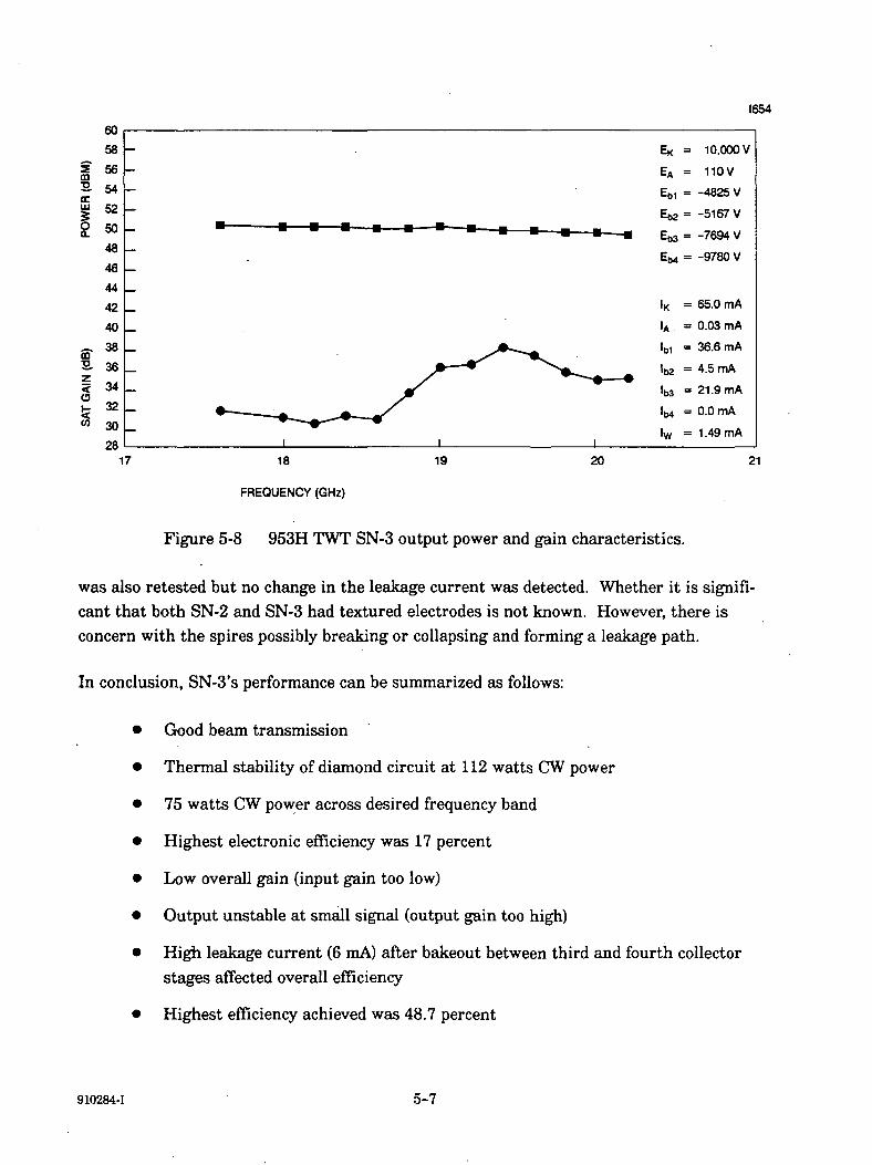
5-7 953H TWT SN-3 efficiency characteristics. 5-6
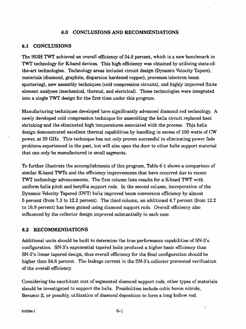
5-8 953H TWT SN-3 output power and gain characteristics. 5-7
VI
LIST OF TABLES
Table Page
3-1 953H Design Features 3-2
3-2 DVT Design Parameters 3-9
3-3 953H Final TWT Design Predicted Overall Efficiency 3-15
3-4 Electron Gun Design Parameters 3-15
4-1 Summary of TWT Configuration 4-3
5-1 Summary of Breadboard TWT Test Results at 17.7 GHz 5-1
6-1 TWT Efficiency Improvements 6-2
vn
1.0 PROGRAM OVERVIEW
1.1 INTRODUCTION
The primary objective of this multiyear effort was to develop and demonstrate a 75 watt,20 GHz, high efficiency traveling wave tube (TWT). A secondary objective was to accom-plish this by incorporating all of the latest technology for improving efficiency into a singleTWT design. Key efficiency enhancement features were: a diamond supported helix, a helixdynamic velocity taper, and a multistage textured graphite collector. Since the TWT wasdeveloped for satellite communication systems, high reliability and long life were alsopriority considerations in the tube design. The TWT developed on this program is Hughesmodel 953H.
The baseline for the 953H was the 918HA TWT, developed under NASA contract numberNAS 3-23345. The 918HA produced 70 watts of output power with 48 percent overallefficiency at 20 GHz. An efficiency of 48 percent is remarkable at K-band frequencies, butincorporating the latest efficiency enhancement features, the 953H TWT attained a newefficiency benchmark of 54.6 percent.
\
1.2 PROGRAM GOALS
The key goals of the program were:
a. Produce 75 watts output from 17.7 to 20.2 GHz.
b. Demonstrate 60 percent overall efficiency.
c. Develop a diamond supported helix circuit with good electrical/thermal charac-teristics.
d. Incorporate a dynamic velocity tapered output circuit pitch for efficiencyenhancement.
e. Incorporate a multistage depressed collector with textured graphite stages forefficiency enhancement.
f. Fabricate and test two proof-of-concept TWTs.
1.3 PROGRAM ACCOMPLISHMENTS
Major accomplishments on the program were the following:
a. The 953H TWT demonstrated over 75 watts of CW power from 1.7.7 to 20.2 GHz.
910284-1 1-1
b. Measured an overall efficiency of 54.6 percent, which is a new high at thisfrequency range.
c. Developed a low-loss diamond circuit with excellent thermal capabilities. Thediamond circuit assembly implements a newly developed cold compressiontechnique1 which eliminates high temperature diamond contamination. Adiamond circuit fabricated with this new technique measured a circuit loss ofapproximately 0.2 dB/inch, several times lower than a typical helix circuit.
d. Developed and implemented a technique of thermally testing the diamond circuitusing a wire cathode in the center of the helix. Results of test circuits showedthe diamond circuit assembly had excellent thermal transfer characteristics.TWTs incorporating diamond circuits confirmed the above by producing poweroutputs in excess of 100 watts CW with no signs of degradation or RF powerfade.
e. Successfully incorporated a dynamic velocity tapered (DVT) helix in the outputcircuit section of the TWT. This technique increases the beam conversionefficiency by maintaining synchronization of the circuit phase velocity with thebeam velocity.
f. Designed and fabricated a four-stage collector with textured graphite electrodes.The first three stages sort and collect the spent electron beam while the fourthstage is a collector spike which operates at cathode potential. Its primaryfunction is to improve electron collection of the other electrodes. Texturedgraphite improve the collector efficiency by reducing secondary electrons.
g. Fabricated and tested three proof-of-concept TWTs. The first tube demonstrateddiamond circuit assembly feasibility and power handling capability. The secondtube demonstrated the 54.6 percent overall efficiency with 100 watts at RFpower. Improved beam conversion efficiency by a refined DVT helix was demon-strated by the third tube, however, a shorted collector stage sacrificed the tube'soverall efficiency performance.
1. Hughes patented.
1-2 9l'0284-I
2.0 DIAMOND ROD TECHNOLOGY
2.1 INTRODUCTION
In a helix type TWT, dielectric material is used to support the helix and provide a thermalpath from the helix to the barrel. The dielectric support material, however, undesirablyalters the electric field pattern of the RF wave on the helix, reducing the field strengthinside the helix where the electron beam-wave interaction takes place. Thus, to optimize thebeam-to-RF conversion efficiency, it is most desirable to use a low dielectric constantmaterial and a minimum amount of material to support the helix.
Diamond is an attractive helix support material due to its low dielectric constant, highcompressive strength, and high thermal conductivity. Because of these features, it ispossible to fabricate a very thin diamond support rod for the helix which is one-half thecross sectional thickness of other dielectric support material such as, boron nitride orberyllia oxide. Diamond support rods as thin as 0.005 inches have been successfullyfabricated and tested in tubes. The thin diamond support rod has resulted in considerablyreduced dielectric loading and improved beam-to-RF conversion efficiency.
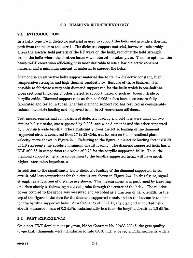
Test measurements and comparison of dielectric loading and cold loss were made on twosimilar helix circuits, one supported by 0.005 inch wide diamonds and the other supportedby 0.020 inch wide beryllia. The significantly lower dielectric loading of the diamondsupported circuit, measured from 17 to 22 GHz, can be seen on the normalized phasevelocity curve shown in Figure 2-1. Referring to the figure, a dielectric loading factor (DLF)of 1.0 represents the absolute minimum circuit loading. The diamond supported helix has aDLF of 0.85 in comparison to a value of 0.73 for the beryllia supported helix. Thus, thediamond supported helix, in comparison to the beryllia supported helix, will have muchhigher interaction impedances.
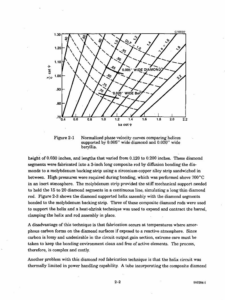
In addition to the significantly lower dielectric loading of the diamond supported helix,circuit cold loss comparisons for this circuit are shown in Figure 2-2. In this figure, signalstrength as a function of distance are shown. This measurement was performed by insertingand then slowly withdrawing a coaxial probe through the center of the helix. The relativepower coupled to the probe was measured and recorded as a function of helix length. In thetop of the figure is the data for the diamond supported circuit and on the bottom is the onefor the beryllia supported helix. At a frequency of 20 GHz, the diamond supported helixcircuit measured losses of 0.2 dB/in; substantially less than the beryllia circuit at 1.5 dB/in.
2.2 PAST EXPERIENCE
On a past TWT development program, NASA Contract No. NAS3-23345, the gem quality(Type II.A.) diamonds were manufactured into 0.010 inch wide rectangular segments with a
910284-1 2-1
ou
1.30
1.20
1.10
1.00
G18507
0.005" WIDE DIAMOND
0.4 0.6 0.8 1.0 1.2 1.4 1.6 1.8 2.0 2.2
Figure 2-1 Normalized phase velocity curves comparing helicessupported by 0.005" wide diamond and 0.020" wideberyllia.
height of 0.030 inches, and lengths that varied from 0.120 to 0.200 inches. These diamondsegments were fabricated into a 3-inch long composite rod by diffusion bonding the dia-monds to a molybdenum backing strip using a zirconium-copper alloy strip sandwiched in
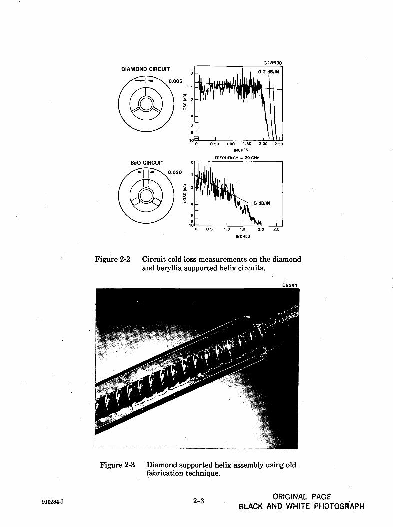
between. High pressures were required during bonding, which was performed above 700 °Cin an inert atmosphere. The molybdenum strip provided the stiff mechanical support neededto hold the 15 to 20 diamond segments in a continuous line, simulating a long thin diamondrod. Figure 2-3 shows the diamond supported helix assembly with the diamond segmentsbonded to the molybdenum backing strip. Three of these composite diamond rods were usedto support the helix and a heat-shrink technique was used to expand and contract the barrel,clamping the helix and rod assembly in place.
A disadvantage of this technique is that fabrication occurs at temperatures where amor-phous carbon forms on the diamond surfaces if exposed to a reactive atmosphere. Sincecarbon is lossy and undesirable in the circuit output gain section, extreme care must betaken to keep the bonding environment clean and free of active elements. The process,therefore, is complex and costly.
Another problem with this diamond rod fabrication technique is that the helix circuit wasthermally limited in power handling capability. A tube incorporating the composite diamond
2-2 910284-1
G18508DIAMOND CIRCUIT
BeO CIRCUIT
0.50 1.00 1.50 2.00 2.50
INCHES
FREQUENCY = 20 GHz
Figure 2-2 Circuit cold loss measurements on the diamondand beryllia supported helix circuits.
E6381
Figure 2-3 Diamond supported helix assembly using oldfabrication technique.
910284-1 2-3 ORIGINAL PAGEBLACK AND WHITE PHOTOGRAPH
rods was fabricated and tested. An improvement in circuit efficiency was demonstrated dueto the reduced dielectric loading of diamonds. However, at RF output levels of about40 watts, a power fade or decrease in power occurred due to overheating of the outputcircuit. Analysis and tests later indicated that the zirconium copper alloy strip that was usedto diffusion bond the diamonds and molybdenum strip, plastically deformed during highpower operation. Consequently, the thermal interfaces between the helix and diamondsupport rods degraded causing the power fade.
2.3 NEW METHODS
The diamonds used in this program are 0.005 inches thick and 0.030 inches high. Suchsmall, translucent parts are difficult to work with. However, a technique has been developedat Hughes Aircraft Company that facilitates circuit manufacturing and resolves problemsexperienced in the past. The technique consists of a special fixture that holds the diamondsegments in place and allows the diamonds to be glued directly onto the helix, eliminatingthe need for a metal backing strip.
This holding fixture was not only used for the assembly of diamonds onto the helix, but alsofor the formation of loss patterns on the diamond rods. These low reflection loss patternsisolate the input and output gain sections and are needed for TWT stability. Usuallypyrolytic carbon is deposited on helix support rods, but due to the high temperaturesinvolved, titanium carbide (TiC) was selected as the lossy material. TiC was deposited withan automated magnetron system at very low temperatures while a metal mask was placedover the diamonds to achieve the desired loss pattern.
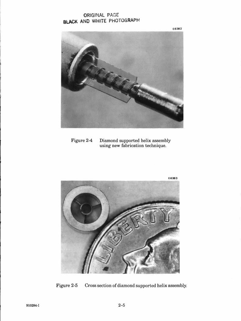
Once the attenuation patterns were sputtered and measured, three diamond rods were gluedonto the helix with lucite. After curing, the metal holding fixture was removed and the helixand diamond rod assembly was placed in a copper sleeve as shown in Figure 2-4. Note thatthe metal strip found in Figure 2-3 has been eliminated.
The diamond circuit assembly implements a newly developed cold compression techniquewhich eliminates heat shrinking and the high temperatures associated with that process.This cold compression technique encapsulates the helix and diamond support assemblyfirmly in place with great pressure on all interfaces. The pressure applied can be precisioncontrolled and the technique is amenable to very small helix circuits which operate up to60 GHz. Cold compression offers several other advantages but the most significant advan-tage is that the entire process is performed at room temperature; eliminating the chances ofcarbon contamination from either lucite or diamond carburization.
After the process of cold compression is complete, the lucite holding the diamond segmentsto the helix is chemically removed. Figure 2-5 shows the cross section of the diamond
- :. . ,..' - ... ,, 2-4 910284-1
ORIGINAL PAG£BLACK AND WHITE PHOTOGRAPH
E6382
Figure 2-4 Diamond supported helix assemblyusing new fabrication technique.
:v : •"""••
rE6383
Figure 2-5 Cross section of diamond supported helix assembly.
910284-1 2-5
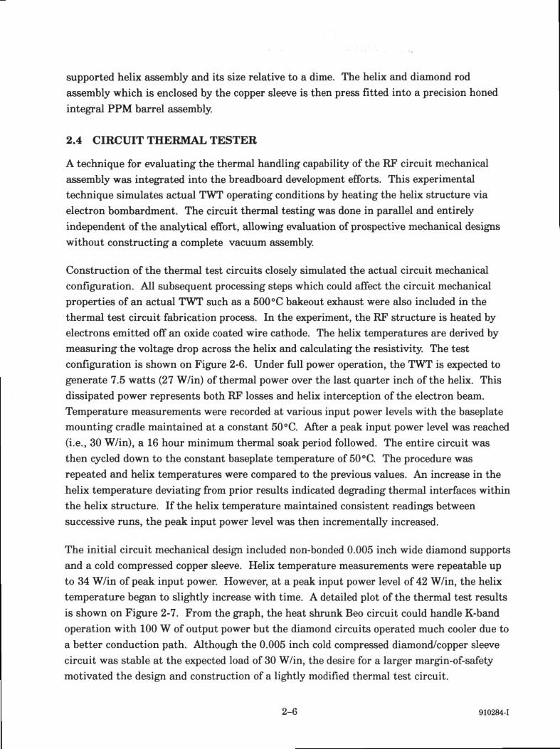
supported helix assembly and its size relative to a dime. The helix and diamond rodassembly which is enclosed by the copper sleeve is then press fitted into a precision honedintegral PPM barrel assembly.
2.4 CIRCUIT THERMAL TESTER
A technique for evaluating the thermal handling capability of the RF circuit mechanicalassembly was integrated into the breadboard development efforts. This experimentaltechnique simulates actual TWT operating conditions by heating the helix structure viaelectron bombardment. The circuit thermal testing was done in parallel and entirelyindependent of the analytical effort, allowing evaluation of prospective mechanical designswithout constructing a complete vacuum assembly.
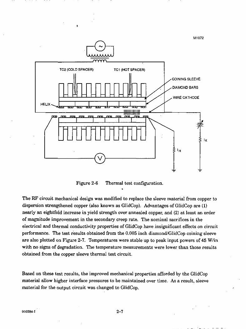
Construction of the thermal test circuits closely simulated the actual circuit mechanicalconfiguration. All subsequent processing steps which could affect the circuit mechanicalproperties of an actual TWT such as a 500 °C bakeout exhaust were also included in thethermal test circuit fabrication process. In the experiment, the RF structure is heated byelectrons emitted off an oxide coated wire cathode. The helix temperatures are derived bymeasuring the voltage drop across the helix and calculating the resistivity. The testconfiguration is shown on Figure 2-6. Under full power operation, the TWT is expected togenerate 7.5 watts (27 W/in) of thermal power over the last quarter inch of the helix. Thisdissipated power represents both RF losses and helix interception of the electron beam.Temperature measurements were recorded at various input power levels with the baseplatemounting cradle maintained at a constant 50°C. After a peak input power level was reached(i.e., 30 W/in), a 16 hour minimum thermal soak period followed. The entire circuit wasthen cycled down to the constant baseplate temperature of 50 °C. The procedure wasrepeated and helix temperatures were compared to the previous values. An increase in thehelix temperature deviating from prior results indicated degrading thermal interfaces withinthe helix structure. If the helix temperature maintained consistent readings betweensuccessive runs, the peak input power level was then incrementally increased.
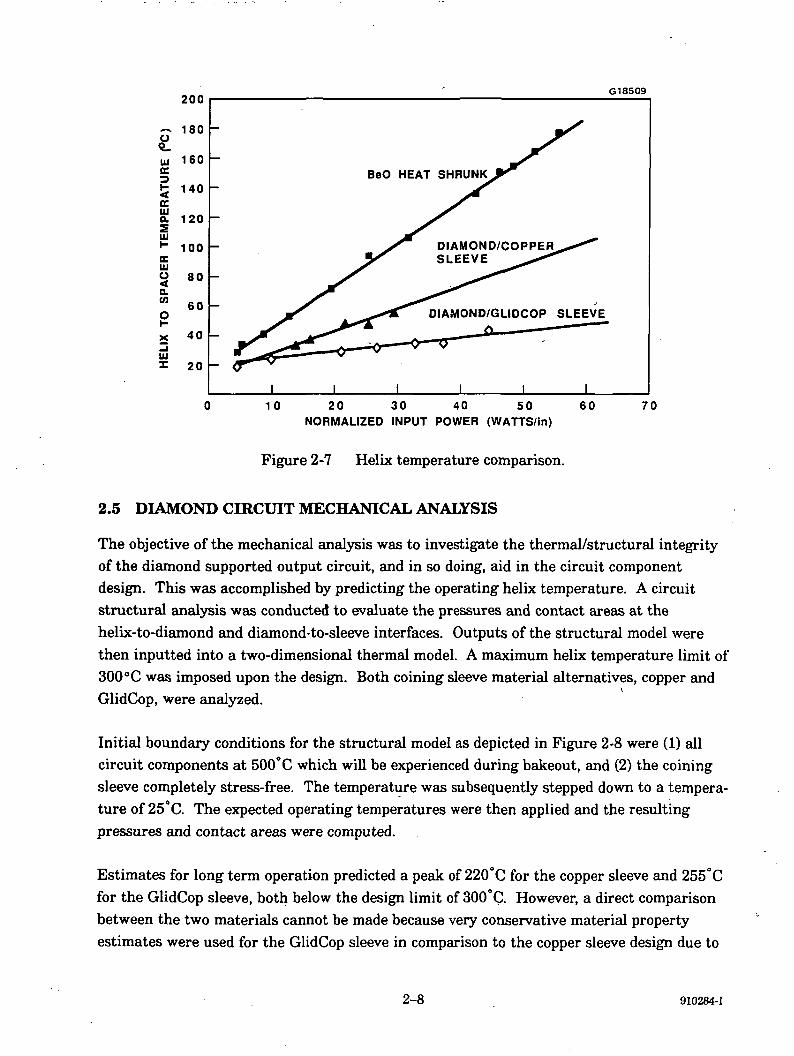
The initial circuit mechanical design included non-bonded 0.005 inch wide diamond supportsand a cold compressed copper sleeve. Helix temperature measurements were repeatable upto 34 W/in of peak input power. However, at a peak input power level of 42 W/in, the helixtemperature began to slightly increase with time. A detailed plot of the thermal test resultsis shown on Figure 2-7. From the graph, the heat shrunk Beo circuit could handle K-bandoperation with 100 W of output power but the diamond circuits operated much cooler due toa better conduction path. Although the 0.005 inch cold compressed diamond/copper sleevecircuit was stable at the expected load of 30 W/in, the desire for a larger margin-of-safetymotivated the design and construction of a lightly modified thermal test circuit.
2-6 910284-1
M1072
_nnrYY\.
TC2 (COLD SPACER) TC1 (HOT SPACER)
HELIX-
COINING SLEEVE
DIAMOND BARS
WIRE CATHODE
Figure 2-6 Thermal test configuration.*
The RF circuit mechanical design was modified to replace the sleeve material from copper todispersion strengthened copper (also known as GlidCop). Advantages of GlidCop are (1)nearly an eightfold increase in yield strength over annealed copper, and (2) at least an orderof magnitude improvement in the secondary creep rate. The nominal sacrifices in theelectrical and thermal conductivity properties of GlidCop have insignificant effects on circuitperformance. The test results obtained from the 0.005 inch diamond/GlidCop coining sleeveare also plotted on Figure 2-7. Temperatures were stable up to peak input powers of 45 W/inwith no signs of degradation. The temperature measurements were lower than those resultsobtained from the copper sleeve thermal test circuit.
Based on these test results, the improved mechanical properties afforded by the GlidCopmaterial allow higher interface pressures to be maintained over time. As a result, sleevematerial for the output circuit was changed to GlidCop.
910284-1 2-7
cc
200
180
160
140
G18509
ocOL 120
UJH 100ocUJu 800.enoXJUJ
60
40
20
BeO HEAT SHRUNK.
DIAMOND/COPPERSLEEVE
DIAMOND/GLIDCOP SLEEVE
I I I10 20 30 40 50
NORMALIZED INPUT POWER (WATTS/in)60 70
Figure 2-7 Helix temperature comparison.
2.5 DIAMOND CIRCUIT MECHANICAL ANALYSIS
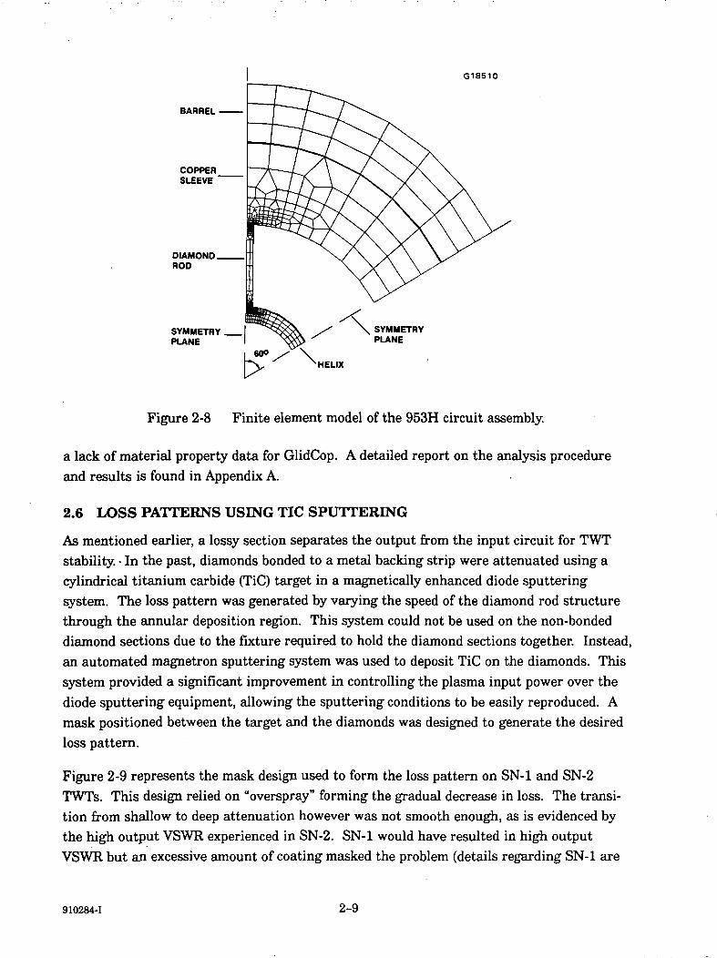
The objective of the mechanical analysis was to investigate the thermal/structural integrityof the diamond supported output circuit, and in so doing, aid in the circuit componentdesign. This was accomplished by predicting the operating helix temperature. A circuitstructural analysis was conducted to evaluate the pressures and contact areas at thehelix-to-diamond and diamond-to-sleeve interfaces. Outputs of the structural model werethen inputted into a two-dimensional thermal model. A maximum helix temperature limit of300°C was imposed upon the design. Both coining sleeve material alternatives, copper and
-\GlidCop, were analyzed.
Initial boundary conditions for the structural model as depicted in Figure 2-8 were (1) allcircuit components at 500° C which will be experienced during bakeout, and (2) the coiningsleeve completely stress-free. The temperature was subsequently stepped down to a tempera-ture of 25"C. The expected operating temperatures were then applied and the resultingpressures and contact areas were computed.
Estimates for long term operation predicted a peak of 220°C for the copper sleeve and 255°Cfor the GlidCop sleeve, both below the design limit of 300°C- However, a direct comparisonbetween the two materials cannot be made because very conservative material propertyestimates were used for the GlidCop sleeve in comparison to the copper sleeve design due to
2-8 910284-1
G18510
BARREL
COPPERSLEEVE
DIAMONDROD
SYMMETRYPLANE
SYMMETRYPLANE
'HELIX
Figure 2-8 Finite element model of the 953H circuit assembly.
a lack of material property data for GlidCop. A detailed report on the analysis procedureand results is found in Appendix A.
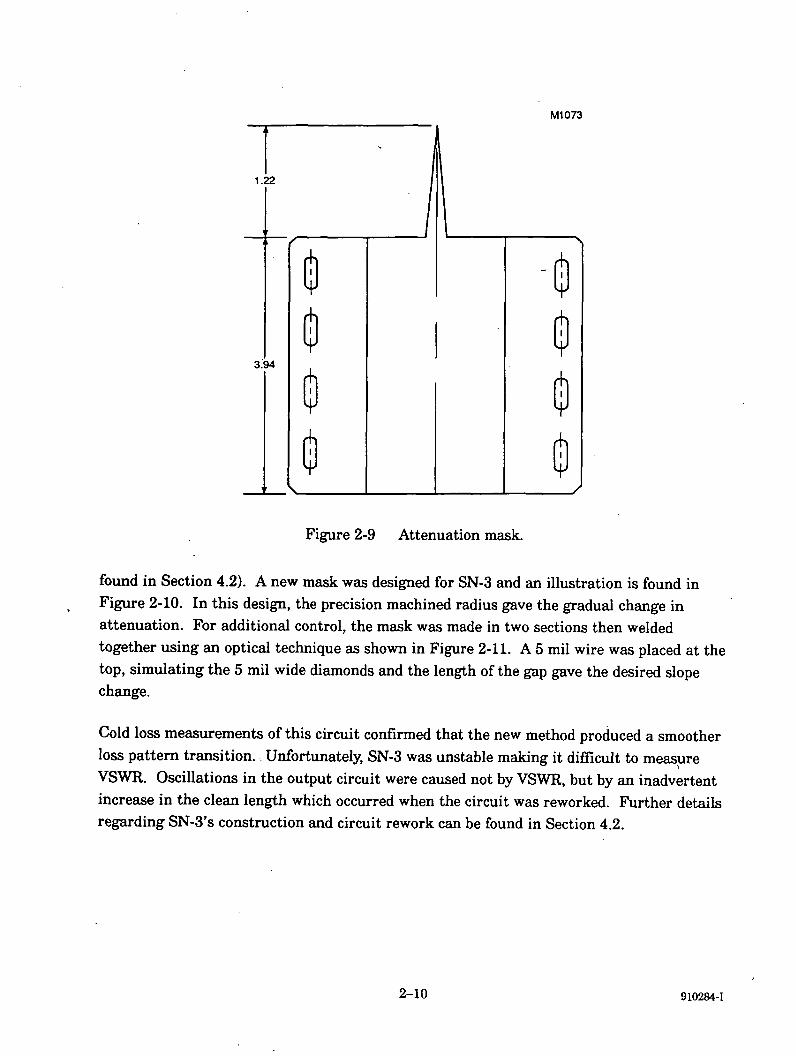
2.6 LOSS PATTERNS USING TIC SPUTTERING
As mentioned earlier, a lossy section separates the output from the input circuit for TWTstability. • In the past, diamonds bonded to a metal backing strip were attenuated using acylindrical titanium carbide (TiC) target in a magnetically enhanced diode sputteringsystem. The loss pattern was generated by varying the speed of the diamond rod structurethrough the annular deposition region. This system could not be used on the non-bondeddiamond sections due to the fixture required to hold the diamond sections together. Instead,an automated magnetron sputtering system was used to deposit TiC on the diamonds. Thissystem provided a significant improvement in controlling the plasma input power over thediode sputtering equipment, allowing the sputtering conditions to be easily reproduced. Amask positioned between the target and the diamonds was designed to generate the desiredloss pattern.
Figure 2-9 represents the mask design used to form the loss pattern on SN-1 and SN-2TWTs. This design relied on "overspray" forming the gradual decrease in loss. The transi-tion from shallow to deep attenuation however was not smooth enough, as is evidenced bythe high output VSWR experienced in SN-2. SN-1 would have resulted in high outputVSWR but an excessive amount of coating masked the problem (details regarding SN-1 are
910284-1 2-9
M1073
1.22
3.94
Figure 2-9 Attenuation mask.
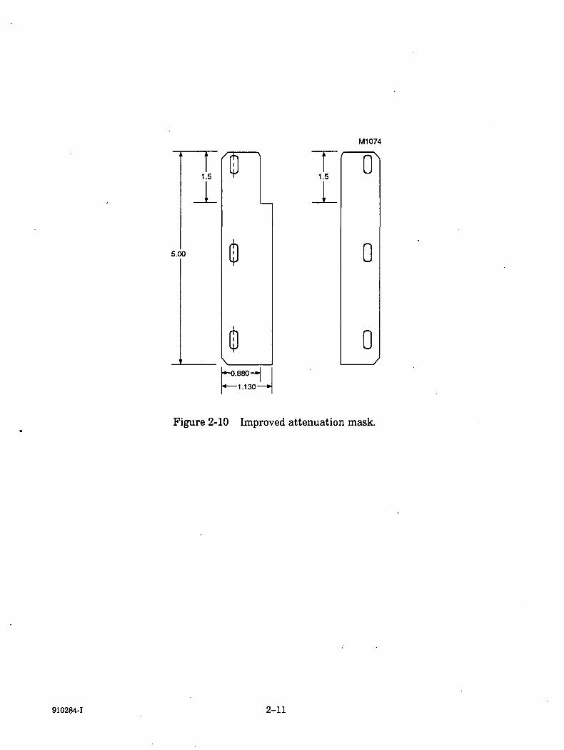
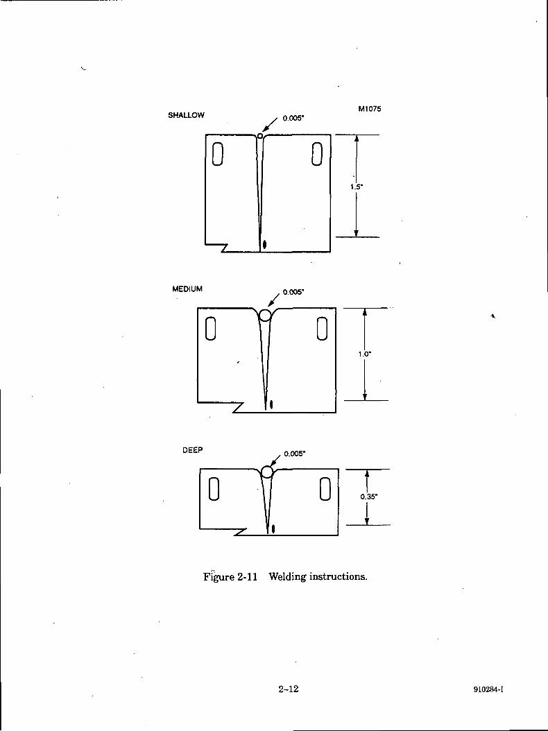
found in Section 4.2). A new mask was designed for SN-3 and an illustration is found inFigure 2-10. In this design, the precision machined radius gave the gradual change inattenuation. For additional control, the mask was made in two sections then weldedtogether using an optical technique as shown in Figure 2-11. A 5 mil wire was placed at thetop, simulating- the 5 mil wide diamonds and the length of the gap gave the desired slopechange.
Cold loss measurements of this circuit confirmed that the new method produced a smootherloss pattern transition. Unfortunately, SN-3 was unstable making it difficult to measureVSWR. Oscillations in the output circuit were caused not by VSWR, but by an inadvertentincrease in the clean length which occurred when the circuit was reworked. Further detailsregarding SN-3's construction and circuit rework can be found in Section 4.2.
2-10 910284-1
M1074
1.5
5.00
1.5
|*-0.880-»|
\*—1.130 —
0
0
0
Figure 2-10 Improved attenuation mask.
910284-1 2-11
SHALLOW
0
M10750.005"
01.5"
MEDIUM
0
0.005"
0
~7 M
1.0"
DEEP
00.005"
0 0.35"
F?gure 2-11 Welding instructions.
2-12 910284-1
3.0 TWT DESIGN
3.1 DESIGN APPROACH
The primary objective of this TWT development effort was high overall efficiency. Otherobjectives considered important were high power capability and low signal distortion. Tosatisfy the primary objective and achieve a reliable design, the design approach was to usethe 918H as the baseline design. The 918H is a 20 GHz, 50 watt helix type space TWT thatwas developed for NASA under Contract No. NAS53-23345. The 918H, as well as this tubedesign, was based upon a low beam perveance approach. As is well known, for low perveancedesigns, beam conversion efficiency are reduced due to lower space charge effects. However,higher overall tube efficiencies can be realized through effective recovery of the spentelectron beam energy. This is one technique for efficiency enhancement; the other efficiencyenhancement techniques were concerned with the interaction circuit.
One of the circuit efficiency enhancement techniques in the TWT design was to increase thecircuit interaction impedance and reduce circuit losses by reducing the dielectric loading ofthe helix support rods. This was accomplished by utilizing very thin sections of diamondwhich support the helix at the critical output area.
A second circuit efficiency enhancement technique was the incorporation of a velocitytapered helix in the large signal region. This technique increases the beam conversionefficiency by maintaining synchronization of the circuit phase velocity with the beamvelocity. The taper is also designed for operation near synchronous voltage which ensureslow signal distortion. This type of velocity taper design approach was developed by Dr. H.Kosmahl, formerly of NASA Lewis Research Center. Known commonly as a dynamic velocitytaper or DVT, this efficiency enhancement technique also provides improved amplitudelinearity near saturation.
The third technique for efficiency enhancement utilized was to maximize the recovery of thespent beam by incorporating a four-stage depressed collector with graphite electrodes. Dueto its material properties, graphite decreases the amount of back-streaming electrons whichreduces the power losses of the spent beam in the collector.
Thus, these three efficiency enhancement techniques when used in conjunction with the lowbeam perveance approach should result in a TWT with high overall efficiencies. This wassupported by analysis that demonstrated that power losses in the collector can be reduced byusing a low beam perveance design approach. In addition, although lower perveance designsgenerally result in lower beam efficiencies, the velocity taper and high impedance diamondcircuit provide sufficient improvement to more than offset any beam efficiency reduction.
910284-1 3-1
In the scaling process, from the 918HA to the 953H, considerations were made for theefficiency enhancement techniques just described in the tube design. For example, since ahigh impedance diamond circuit was used in the design, a higher beam conversion efficiencywas used in the computations. The results of these computations are summarized inTable 3-1, which shows design features for the 953H as well as the 918H.
The following sections will describe the efficiency enhancement techniques that are used inthe 953H and then the electron gun and PPM designs will also be discussed.
3.2 RF CIRCUIT DESIGN
A two-section input circuit is used in the 953H TWT. The two sections are used because ofthe high gain requirement for the TWT and each section will be short enough so thatbackward-wave oscillation (BWO) problems will not be encountered. Since the input circuitprovides only gain and is quite long; the lower impedance beryllia supported helix circuit is
TABLE 3-1953H DESIGN FEATURES
Parameter
Frequency (GHz)
Gun Perveance (uP)
Operating Voltage (kV)
Cathode
rgs (minimum)
Helix diameter (2a)
Helix tape size
Helix support material
Helix support size
Collector stages
Collector electrodematerial
Magnetic Field (G)
X p /L
918HA(Baseline Design)
17.7 - 21.2
0.065
-10.7
TypeM
0.0101"
0.047"
0.007" x 0.020"
Beryllia
0.020" x 0.037"
JAI currentcollecting stagesplus a spike
TiC coatingon copper
2700
5.00
953H
17.7 - 20.2
0.053
-9.7
TypeM
0.0082"
0.47"
0.006" x 0.015"
Diamond IIA
0.005" x 0.030"
" ?3> currentcollecting stagesplus a spike
POCO graphite
3500
3.25
3-2 910284-1
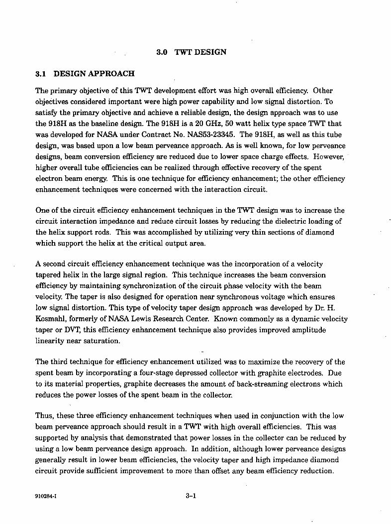
used. This approach was chosen primarily for cost effectiveness. A cross sectional drawingof the 953H input circuit assembly is shown in Figure 3-1.
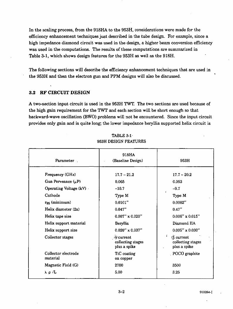
Figure 3-2 shows the cross sectional drawing of the 953H output circuit assembly. Asdiscussed previously, this helix circuit uses very thin diamond support bars which results inhigh interaction impedances and low circuit losses.
3.3 VELOCITY TAPERED HELIX
The output RF circuit incorporates a DVT helix. The principal objective behind the DVT isto optimize the interaction process between the traveling RF circuit wave and the electronbeam. By maintaining synchronization of the circuit and electron beam phase velocitiesthroughout the entire circuit length, the transfer of kinetic energy is maximized.
A measure of the synchronization between the RF circuit wave and electron beam isindicated by Pierce's velocity parameter. In the small signal region of the circuit, thebunched electron beam is well defined. Here, the small signal gain and the velocity parame-ter can be accurately determined. When the beam enters the large signal gain region, theelectrons exponentially transfer their kinetic energy to the RF wave as a function of axial
1639BeO SUPPORT ROD (3)0.020" X 0.030" 0.22" THICK BARREL
(IRON POLE PIECE/MONEL SPACER)
0.112"
TUNGSTENTAPE HELIX0.015" x 0.006"PITCH = 0.0323"
0.030" THICKCOPPER SLEEVE
RHENIUM
Figure 3-1 Cross-section of the 953H input circuit assembly.
910284-1 3-3
1640
DIAMOND SUPPORT ROD (3)0.005" x 0.030" 0.22" THICK BARREL
(IRON POLE PIECE/MONEL SPACER)
TUNGSTENTAPE HEUX0.015" x 0.006"PITCH = 0.0282"
0.030" THICKGUDCOP SLEEVE
RHENIUM
Figure 3-2 Cross-section of the 953H output circuit assembly.
distance. At the transition from small signal to large signal, the taper is initiated. Thevelocity parameter as a function of distance is maintained close to zero by exponentiallydecreasing the helix pitch as the electron beam velocity decreases.
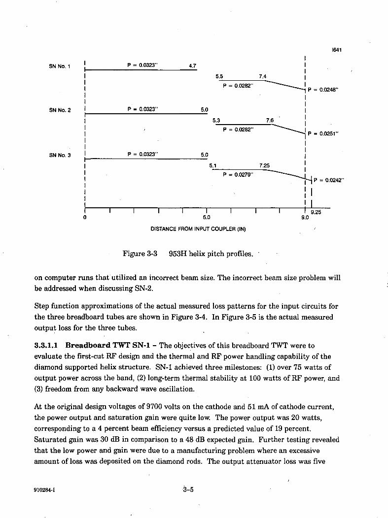
3.3.1 Comparison Between Computed and Measured DVT Designs
Figure 3-3 shows the helix pitch profiles for the three breadboard TWTs that were built andtested during this development program. As seen in the figure, the input circuit section forthe TWTs are quite long and this occurs because the input is made into two sections for thehigh gain requirement. The two active input sections are electrically isolated by attenuatorsand each of them are quite short for BWO stability.
In the output circuit, a section which precedes the DVT section has been denoted as thedriver section. The driver section pitch for the first two breadboard tubes was chosen for0 percent over-voltaging. Also note in Figure 3-3, that the first two breadboard tubes usedlinearly tapered DVT circuits with tapered pitches of 12 and 11 percent, respectively. Thelinear tapered DVT circuits were initially used since computations at that time indicatedthat linear tapered helix was equivalent to an exponential design and that no additionalefficiency could be achieved with the exponential taper. That conclusion however, was based
3-4 910284-1
SN No. 1
SN No. 2
SN No. 3
P = 0.0323" 4.7
P = 0.0323"
P = 0.0323"
5.5 7.4
P = 0.0282"
5.0
5.3 7.6
P = 0.0282"
5.0
5.1 7.25
P = 0.0279"
1 I I I5.0
DISTANCE FROM INPUT COUPLER (IN)
1641
P = 0.0248"
P = 0.0251"
P = 0.0242"
9.25
Figure 3-3 953H helix pitch profiles.
on computer runs that utilized an incorrect beam size. The incorrect beam size problem willbe addressed when discussing SN-2.
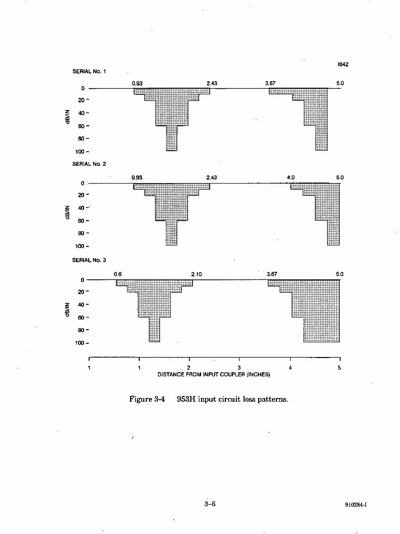
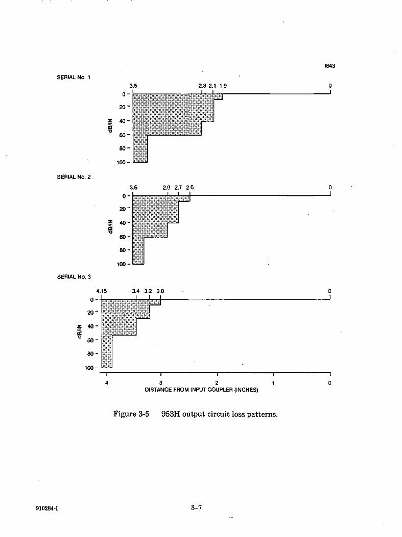
Step function approximations of the actual measured loss patterns for the input circuits forthe three breadboard tubes are shown in Figure 3-4. In Figure 3-5 is the actual measuredoutput loss for the three tubes.
3.3.1.1 Breadboard TWT SN-1 - The objectives of this breadboard TWT were toevaluate the first-cut RF design and the thermal and RF power handling capability of thediamond supported helix structure. SN-1 achieved three milestones: (1) over 75 watts ofoutput power across the band, (2) long-term thermal stability at 100 watts of RF power, and(3) freedom from any backward wave oscillation.
At the original design voltages of 9700 volts on the cathode and 51 mA of cathode current,the power output and saturation gain were quite low. The power output was 20 watts,corresponding to a 4 percent beam efficiency versus a predicted value of 19 percent.Saturated gain was 30 dB in comparison to a 48 dB expected gain. Further testing revealedthat the low power and gain were due to a manufacturing problem where an excessiveamount of loss was deposited on the diamond rods. The output attenuator loss was five
910284-1 3-5
SERIAL No. 1
20-
f. 40-ffl
* 60-
80-
100-
SERIAL No. 2
§
20-
40-
60-
80-
100-
SERIAL No. 3
m
20-
40-
60-
80-
100-
0.93
0.93
0.6
2.43 3.67
I642
5.0
2.43 4.0 5.0
2.10 3.67 5.0
2 3DISTANCE FROM INPUT COUPLER (INCHES)
Figure 3-4 953H input circuit loss patterns.
3-6 910284-1
I643
SERIAL No. 1
3
o-
20-
Afl —Hw
fifl —uu
80-
inn -
5 2.3 2.1 1.9 0I I I
!
SERIAL No. 2
3.5 2.9 2.7 2.5
0-
20-
Z 40-m•a
60-
80-
100-
I
SERIAL No. 3
zffi•a
4.
o —
20-
40-
60-
80-
100-
5 3.4 3.2 3.0 0
I ' '
^—
3 2DISTANCE FROM INPUT COUPLER (INCHES)
Figure 3-5 953H output circuit loss patterns.
910284-1 3-7
times greater than required. This attenuator pattern resulted in a very short output circuitsection, hence, poor beam efficiency and low gain occurred.
3.3.1.2 Breadboard TWT SN-2 - This tube achieved the highest overall efficiencyrecorded for a K-band TWT; 54.6 percent. The overall efficiency goal of 60 percent however,was not met because the basic efficiency was 16.9 percent instead of the expected 20 percent.A thorough review of the design process revealed that the circuit had been designed using animproper beam size.
In the DVT code, balanced flow is based upon the Brillouin equation given by:
0.462* [(V0)*(Po)]-5
where: r is beam radius in inches
V0 is beam voltage in volts
P0 is beam perveance in micropervs
is peak magnetic field in gauss
Thus, for a given beam voltage, beam perveance and peak magnetic field, the beam radius isdefined by the above equation to achieve balanced flow. If the beam size used is not consis-tent with the above equation, then a large amount of rippling will occur in the electronbeam. The amount of rippling would depend upon how deviant the inputted beam radiuswas from the balanced flow condition.
Historically, the DVT code was ran by using the actual beam voltages, beam perveances andthe peak magnetic fields. The beam radius that was then inputted in these cases were thencalculated using the above equation and this beam radius has been defined as the "non-thermal" beam radius. When the DVT code was operated in this manner, good agreementbetween calculation and measured data occurred.
Unfortunately, in the early phase of the 953H development program, an incorrect beam size,not consistent with the above equation, was used in the computations. The incorrect beamsize corresponded to a beam radius which encompasses 95 percent of the thermal electronbeam. In this case, the magnetic field was not consistent with the beam size because theBrillauin equation was not used. Computer results predicted 20 percent basic efficiency andno indication of a problem was apparent. A revision, however, was made to the DVTprogram which plots the electron beam. From these plots severe beam rippling and largecircuit beam interception were exhibited. Also, when the DVT code was operated in this
3-8 910284-1
manner, the computations indicated no differences in calculated efficiencies between linearand exponential tapers. Once the discrepancy between predicted and measured beamefficiency was understood the design for breadboard No. 3 was performed. For generalinformation, Table 3-2 contains the design parameters as entered into the DVT code for eachoftheTWTs.
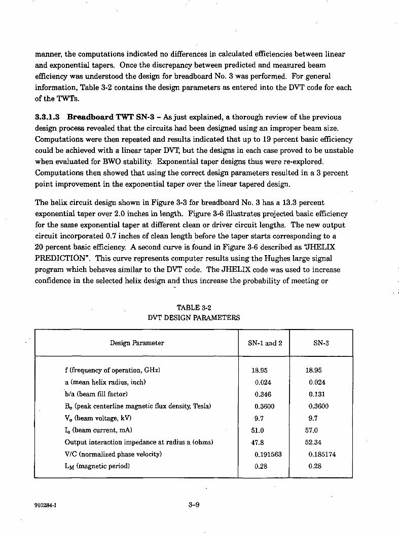
3.3.1.3 Breadboard TWT SN-3 - As just explained, a thorough review of the previousdesign process revealed that the circuits had been designed using an improper beam size.Computations were then repeated and results indicated that up to 19 percent basic efficiencycould be achieved with a linear taper DVT, but the designs in each case proved to be unstablewhen evaluated for BWO stability. Exponential taper designs thus were re-explored.Computations then showed that using the correct design parameters resulted in a 3 percentpoint improvement in the exponential taper over the linear tapered design.
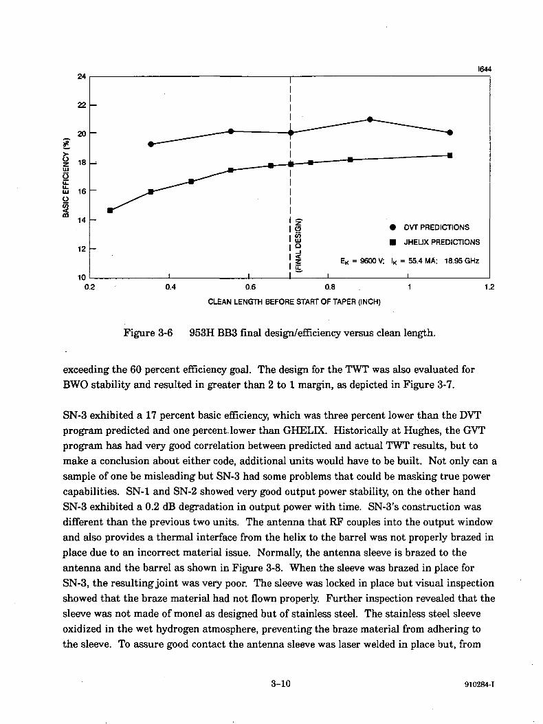
The helix circuit design shown in Figure 3-3 for breadboard No. 3 has a 13.3 percentexponential taper over 2.0 inches in length. Figure 3-6 illustrates projected basic efficiencyfor the same exponential taper at different clean or driver circuit lengths. The new outputcircuit incorporated 0.7 inches of clean length before the taper starts corresponding to a20 percent basic efficiency. A second curve is found in Figure 3-6 described as "JHELIXPREDICTION". This curve represents computer results using the Hughes large signalprogram which behaves similar to the DVT code. The JHELIX code was used to increaseconfidence in the selected helix design and thus increase the probability of meeting or
TABLE 3-2DVT DESIGN PARAMETERS
Design Parameter
f (frequency of operation, GHz)
a (mean helix radius, inch)
b/a (beam fill factor)
B0 (peak centerline magnetic flux density, Tesla)
V0 (beam voltage, kV)
Io (beam current, mA)
Output interaction impedance at radius a (ohms)
V/C (normalized phase velocity)
LM (magnetic period)
SN-1 and 2
18.95
0.024
0.346
0.3600
9.7
51.0
47.8
0.191563
0.28
SN-3
18.95
0.024
0.131
0.3600
9.7
57.0
52.34
0.185174
0.28
910284-1 3-9
O
24
22
20
18
1644
uJ 16O
14
12
10
• DVT PREDICTIONS
• JHELIX PREDICTIONS
EK = 9600V; IK = 55.4 MA; 18.95 GHz
0.2 0.4 0.6 0.8 1
CLEAN LENGTH BEFORE START OF TAPER (INCH)
1.2
Figure 3-6 953H BBS final design/efficiency versus clean length.
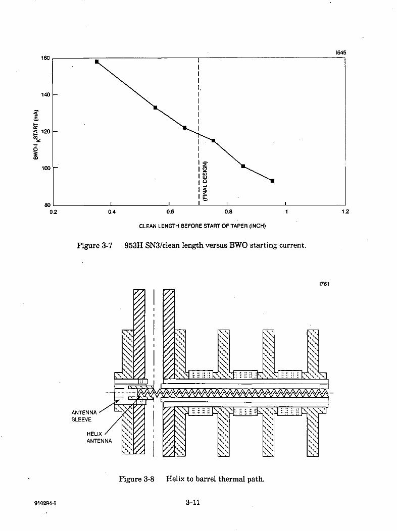
exceeding the 60 percent efficiency goal. The design for the TWT was also evaluated forBWO stability and resulted in greater than 2 to 1 margin, as depicted in Figure 3-7.
SN-3 exhibited a 17 percent basic efficiency, which was three percent lower than the DVTprogram predicted and one percent-lower than GHELIX. Historically at Hughes, the GVTprogram has had very good correlation between predicted and actual TWT results, but tomake a conclusion about either code, additional units would have to be built. Not only can asample of one be misleading but SN-3 had some problems that could be masking true powercapabilities. SN-1 and SN-2 showed very good output power stability, on the other handSN-3 exhibited a 0.2 dB degradation in output power with time. SN-3's construction wasdifferent than the previous two units. The antenna that RF couples into the output windowand also provides a thermal interface from the helix to the barrel was not properly brazed inplace due to an incorrect material issue. Normally, the antenna sleeve is brazed to theantenna and the barrel as shown in Figure 3-8. When the sleeve was brazed in place forSN-3, the resulting joint was very poor. The sleeve was locked in place but visual inspectionshowed that the braze material had not flown properly. Further inspection revealed that thesleeve was not made of monel as designed but of stainless steel. The stainless steel sleeveoxidized in the wet hydrogen atmosphere, preventing the braze material from adhering tothe sleeve. To assure good contact the antenna sleeve was laser welded in place but, from
3-10 910284-1
0.2 0.4 0.6 0.8
CLEAN LENGTH BEFORE START OF TAPER (INCH)
Figure 3-7 953H SN3/clean length versus BWO starting current.
1761
ANTENNA•
SLEEVE
1y////
////.
\ • • : • J
11, V
11s \ W
/////A
HELIX
ANTENNA IT?/xk\ ::;;̂ ;
^
,̂ ES^-1
Figure 3-8 Helix to barrel thermal path.
910284-1 3-11
SN-3's performance the interface proved to be a poor thermal path from the helix to thebarrel. The output circuit could not be rebuilt due to end of contract restrictions.
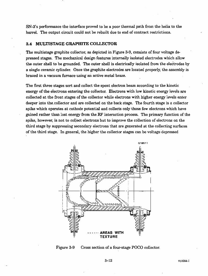
3.4 MULTISTAGE GRAPHITE COLLECTOR
The multistage graphite collector, as depicted in Figure 3-9, consists of four voltage de-pressed stages. The mechanical design features internally isolated electrodes which allowthe outer shell to be grounded. The outer shell is electrically isolated from the electrodes bya single ceramic cylinder. Once the graphite electrodes are located properly, the assembly isbrazed in a vacuum furnace using an active metal braze.
The first three stages sort and collect the spent electron beam according to the kineticenergy of the electrons entering the collector. Electrons with low kinetic energy levels arecollected at the front stages of the collector while electrons with higher energy levels enterdeeper into the,collector and are collected on the back stage. The fourth stage is a collectorspike which operates at cathode potential and collects only those few electrons which havegained rather than lost energy from the RF interaction process. The primary function of thespike, however, is not to collect electrons but to improve the collection of electrons on thethird stage by suppressing secondary electrons that are generated at the collecting surfacesof the third stage. In general, the higher the collector stages can be voltage depressed
G18511
AREAS WITHTEXTURE
Figure 3-9 Cross section of a four-stage POCO collector.
3-12 910284-1
without generating undesirable back-streaming electrons, the greater the recovery of spentbeam energy. This reduces the TWT dc power consumption and thereby increases the TWToverall efficiency.
Back-streaming electrons increase the thermal loading of the output circuit and reduce TWToverall efficiency. Therefore, minimizing these electrons is one of the objectives in goodcollector design. Isotropic graphite was selected as the electrode material because of its lowreflected primary electron yield index and secondary electron emission ratio. The reflectedprimary electron yield index is two to five times lower than copper and the secondaryelectron emission ratio is about one-half. These key properties of graphite significantlyreduce back-streaming electrons and typically improve overall TWT efficiency by three tofour percentage points. Ion-texturing the critical surfaces of the graphite electrodes furtherimproves the overall TWT efficiency by about one percentage point.
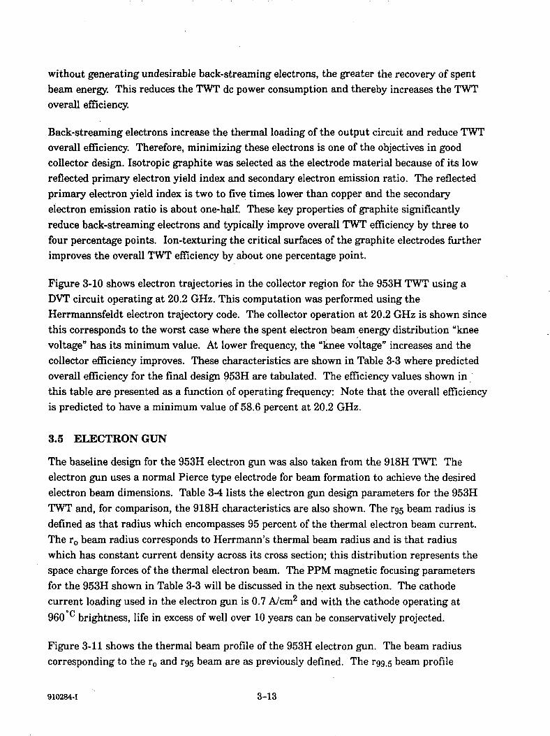
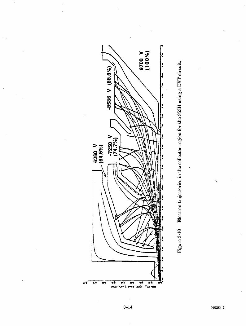
Figure 3-10 shows electron trajectories in the collector region for the 953H TWT using aDVT circuit operating at 20.2 GHz. This computation was performed using theHerrmannsfeldt electron trajectory code. The collector operation at 20.2 GHz is shown sincethis corresponds to the worst case where the spent electron beam energy distribution "kneevoltage" has its minimum value. At lower frequency, the "knee voltage" increases and thecollector efficiency improves. These characteristics are shown in Table 3-3 where predictedoverall efficiency for the final design 953H are tabulated. The efficiency values shown inthis table are presented as a function of operating frequency: Note that the overall efficiencyis predicted to have a minimum value of 58.6 percent at 20.2 GHz.
3.5 ELECTRON GUN
The baseline design for the 953H electron gun was also taken from the 918H TWT. Theelectron gun uses a normal Pierce type electrode for beam formation to achieve the desiredelectron beam dimensions. Table 3-4 lists the electron gun design parameters for the 953HTWT and, for comparison, the 918H characteristics are also shown. The r^ beam radius isdefined as that radius which encompasses 95 percent of the thermal electron beam current.The r0 beam radius corresponds to Herrmann's thermal beam radius and is that radiuswhich has constant current density across its cross section; this distribution represents thespace charge forces of the thermal electron beam. The PPM magnetic focusing parametersfor the 953H shown in Table 3-3 will be discussed in the next subsection. The cathodecurrent loading used in the electron gun is 0.7 A/cm2 and with the cathode operating at
o /~\
960 u brightness, life in excess of well over 10 years can be conservatively projected.
Figure 3-11 shows the thermal beam profile of the 953H electron gun. The beam radiuscorresponding to the r0 and rg$ beam are as previously defined. The rgg^ beam profile
910284-1 3-13
ot-,
p03
COw050>
-i->t-i
co•a2
<D
£_g
ico
o
CD
S
COd>
I
3-14 910284-1
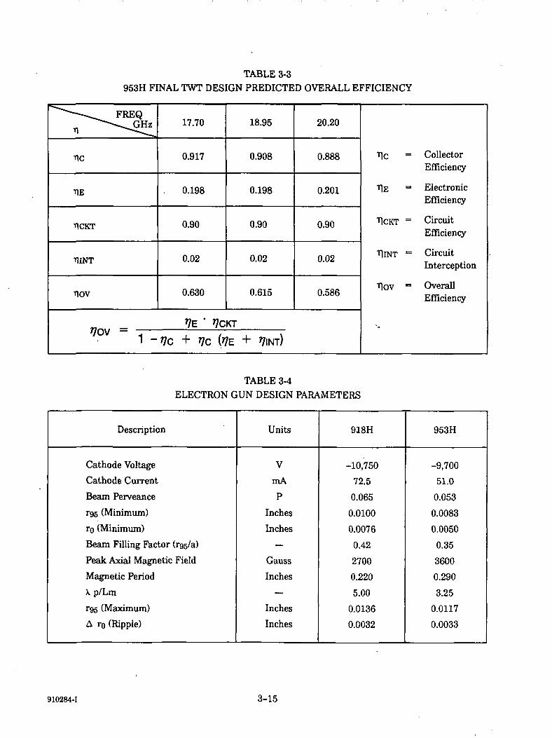
TABLE 3-3953H FINAL TWT DESIGN PREDICTED OVERALL EFFICIENCY
"""•̂ --.̂ FREQ
^^-^GH^
TIC
TIE
T1CKT
TIINT
11OV
17.70
0.917
. 0.198
0.90
0.02
0.630
18.95
0.908
0.198
0.90
0.02
0.615
*7E ' *?CKTMV 1 -1C + rjc (TIE + ^INT)
20.20
0.888
0.201
0.90
0.02
0.586
T|c = CollectorEfficiency
T|E = ElectronicEfficiency
TICKT = CircuitEfficiency
"HINT = CircuitInterception
T|ov = OverallEfficiency
V
TABLE 3-4ELECTRON GUN DESIGN PARAMETERS
Description
Cathode Voltage
Cathode Current
Beam Perveance
rgs (Minimum)
TO (Minimum)
Beam Filling Factor (rgs/a)
Peak Axial Magnetic Field
Magnetic Period
X p/Lm
rgs (Maximum)
A TO (Ripple)
Units
V
mA
P
Inches
Inches
—
Gauss
Inches
—Inches
Inches
918H
-10,750
72.5
0.065
0.0100
0.0076
0.42
2700
0.220
5.00
0.0136
0.0032
953H
-9,700
51.0
0.053
0.0083
0.0050
0.35
3600
0.290
3.25
0.0117
0.0033
910284-1 3-15
0.80 i
0.70
0.60
G18512
_ 0.50coaiXuz=• 0.40CO2Q
* 0.30
UJCO
0.20
0.10
0.00
E|< - 9700 V
P = 0.053 ,iP
rg5 (MIN) = 0.0083"
/ r99.5
' ,'95
J_ _L
0.00 0.25 0.50 0.75 1.00
DISTANCE FROM CATH (INCHES)
1.25
Figure 3-11 953H gun thermal beam profile.
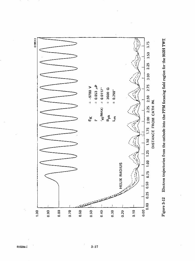
corresponds to the beam radius which contains 99.5 percent of the electron beam current.Figure 3-12 shows beam trajectories from the cathode into the PPM focusing field region.Note in the figure the well behaved electron trajectories and the maximum values are allwithin the inner diameter of the helix radius.
3.6 PPM DESIGN
As shown in Table 3-4, the 953H electron beam is focused using a PPM design with a peakfield of 3600 gauss. The PPM magnet period is 0.290 inches, thus resulting in a plasma-wavelength to magnet period ratio of 3.25. This is a conservative value for the plasma-wavelength to magnet period ratio and was so chosen to assure excellent beam containment.The PPM stack uses samarium-cobalt magnets which are temperature compensated so that
3-16 910284-1
II-<o
OccU-
LLJO
CO
CO0)
910284-1 3-17
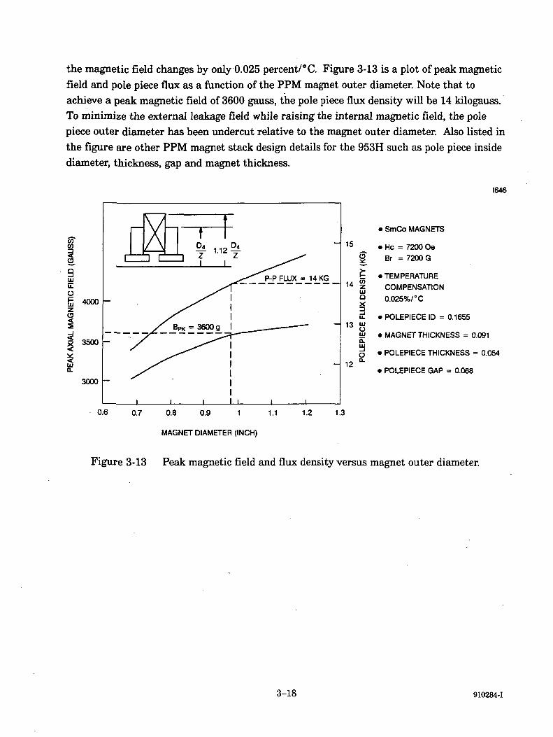
the magnetic field changes by only 0.025 percent/°C. Figure 3-13 is a plot of peak magneticfield and pole piece flux as a function of the PPM magnet outer diameter. Note that toachieve a peak magnetic field of 3600 gauss, the pole piece flux density will be 14 kilogauss.To minimize the external leakage field while raising the internal magnetic field, the polepiece outer diameter has been undercut relative to the magnet outer diameter. Also listed inthe figure are other PPM magnet stack design details for the 953H such as pole piece insidediameter, thickness, gap and magnet thickness.
1646
co
9UJu.O
C3S_i
4000
3500
3000
15
14UJQ
13
• SmCo MAGNETS
• Ho = 7200 Oe
Br = 7200 G
• TEMPERATURECOMPENSATION
0.025%/°C
• POLEPIECE ID = 0.1655
• MAGNET THICKNESS = 0.091
125 • POLEPIECE THICKNESS = 0.054Q_
• POLEPIECE GAP = 0.068
0.6 0.7 0.8 0.9 1 1.1
MAGNET DIAMETER (INCH)
1.2 1.3
Figure 3-13 Peak magnetic field and flux density versus magnet outer diameter.
3-18 910284-1
4.0 TWT CONFIGURATION
4.1 INTRODUCTION
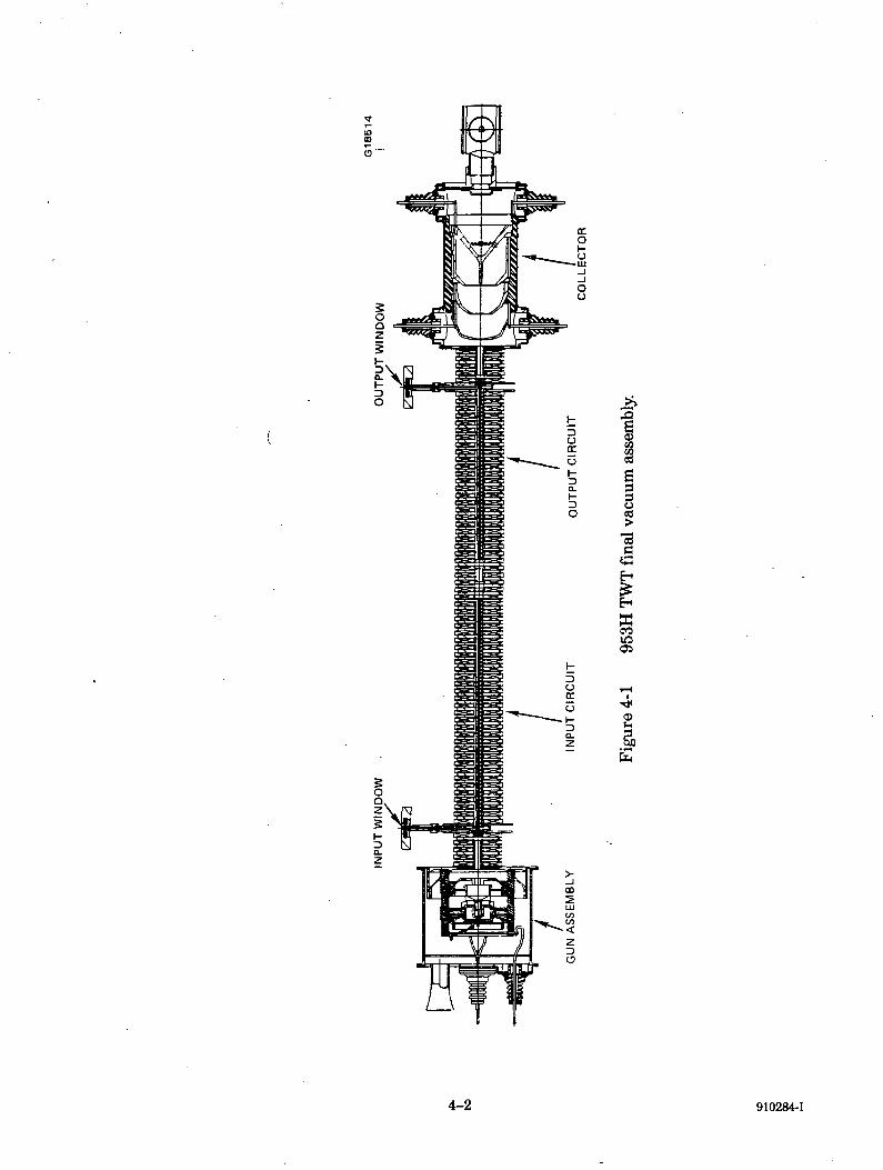
As depicted in the TWT's cross-sectional view found in Figure 4-1, the 953H mechanical gundesign utilizes internally isolated electrodes which allow the outer shell to be grounded.This design eliminated the need for high voltage potting material and the associatedproblems. The inner gun is a stacked brazed assembly which has demonstrated highperformance under adverse shock and vibration conditions. Direct helix-to-waveguidecoupling was employed to minimize RF losses. In this design an antenna, or metal cylinderbrazed to the helix provides the coupling mechanism to a half height waveguide. Thefour-stage collector also utilized internally isolated electrodes allowing the shell to begrounded. The grounded shell along with conservative voltage stresses significantly contrib-uted to the overall reliability of the TWT.
Three vacuum assemblies were built under this program. Each assembly had a slightlydifferent configuration and Table 4-1 lists the major differences between each TWT.
4.2 CONFIGURATION BY SERIAL NUMBER
SN-l's Vacuum Assembly was completed in March of 1988. Testing of this unit revealed thatthere was an insufficient amount of output gain. Investigation into this problem suggestedthat an excessive amount of TiC was sputtered onto the diamonds in the process of creatingthe desired loss patterns. Loss measurements were performed on the composite diamondrods using a slotted line fixture. The fixture is made up of a helix circuit with a longitudinalslot in the 6uter conductor through which a probe on a carriage is inserted. The lossrelative to position along the helix is then obtained by moving the carriage along the slotand reading the power coupled into the probe. The differences in the fixture circuit and the953H design however were not accounted for. Thus, five times the expected loss wasdeposited on the diamond support rods. For SN-2, the problem of excessive loss waseliminated by applying the appropriate correction factors. Figures 3-4 and 3-5 in theprevious section illustrate the approximate attenuation patterns for each breadboard TWT.
The original DVT design assumed non-realistic loss patterns; 5 dB/in loss under the attenu-ator pattern and an abrupt increase to 100 dB/in. The DVT program assumes a perfectlymatched circuit, but in an actual TWT this loss pattern would create a large mismatch and,consequently, a large amount of reflected power. To better simulate real hardware a morepractical pattern was entered into the DVT program and the optimal helix pitch wasrecomputed and incorporated into SN-2. This accounts for the small change in the helixprofiles found in Figure 3-3. The input length increased by 0.3 inch and the output helix by0.2 inch.
910284-1 4-1
Tl<
I
4-2 910284-1
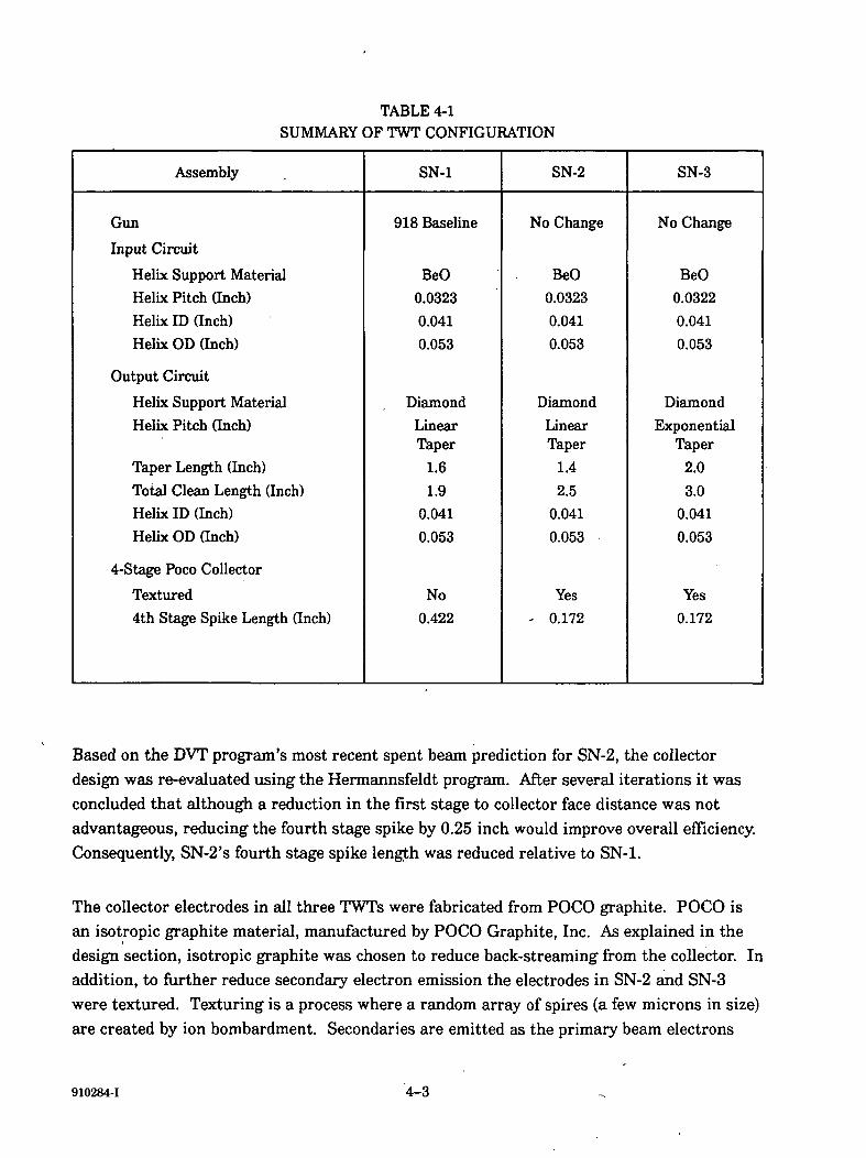
TABLE 4-1SUMMARY OF TWT CONFIGURATION
Assembly
Gun
Input Circuit
Helix Support MaterialHelix Pitch (Inch)Helix ID (Inch)Helix OD (Inch)
Output Circuit
Helix Support MaterialHelix Pitch (Inch)
Taper Length (Inch)
Total Clean Length (Inch)Helix ID (Inch)Helix OD (Inch)
4-Stage Poco Collector
Textured4th Stage Spike Length (Inch)
SN-1
918 Baseline
BeO0.03230.0410.053
DiamondLinearTaper
1.6
1.90.041
0.053
No0.422
SN-2
No Change
BeO0.03230.041
0.053
DiamondLinearTaper
1.4
2.50.041
0.053
Yes- 0.172
SN-3
No Change
BeO0.03220.041
0.053
Diamond
ExponentialTaper
2.03.0
0.041
0.053
Yes0.172
Based on the DVT program's most recent spent beam prediction for SN-2, the collectordesign was re-evaluated using the Hermannsfeldt program. After several iterations it wasconcluded that although a reduction in the first stage to collector face distance was notadvantageous, reducing the fourth stage spike by 0.25 inch would improve overall efficiency.Consequently, SN-2's fourth stage spike length was reduced relative to SN-1.
The collector electrodes in all three TWTs were fabricated from POCO graphite. POCO isan isotropic graphite material, manufactured by POCO Graphite, Inc. As explained in thedesign section, isotropic graphite was chosen to reduce back-streaming from the collector. Inaddition, to further reduce secondary electron emission the electrodes in SN-2 and SN-3were textured. Texturing is a process where a random array of spires (a few microns in size)are created by ion bombardment. Secondaries are emitted as the primary beam electrons
910284-1 4-3
collide with the electrode surface but due to the geometry of the spires the secondaries arerepeatedly intercepted by other electrons.
In summary, the following changes were made from SN-1 to SN-2:
• output circuit gain length increased 0.6 inch
• helix taper length was reduced 0.2 inch
• collector spike length decreased 0.3 inch
• POCO stages textured
SN-2 had very good RF performance, but the goal of 60 percent overall efficiency was notmet. Historically at EDD, the DVT program had predicted one to two percent points lowerthan actual TWT results. In this case, the DVT program prediction was on the averageseven percent higher than actual TWT results. Review of the input parameters used todesign SN-1 and SN-2's DVT helix revealed an incorrect beam size. After the appropriatecorrections were made to the DVT program, SN-3's output helix was redesigned. Detailsregarding the circuit design problem are found in Section 3.3.1.2.
SN-2's RF performance (43 dB of gain and 54.6 percent overall efficiency) confirmed that theexcessive loss found in SN-l's output circuit was eliminated by applying the appropriatecorrection factors. However, the high loss in SN-1 masked a second problem. The losspattern produced by the TiC sputtering fixture was too abrupt. Specifically, the transitionfrom the shallow loss pattern to the deep pattern was not smooth. The abrupt change inslope created a reflection or mismatch which was amplified through regeneration affects.The problem surfaced as high ripple in the cold VSWR data for the output circuit.
It was decided to repair the output circuit. This allowed verification of the circuit redesigneffort in a timely fashion and at a reasonable cost to the program. In addition, the alterna-tive to rework SN-2 with a new output circuit at a later date was still a possibility. Thenetwork entailed the addition of lossy material onto the diamond attenuation pattern.Aguedag, which is an agueous colloidal suspension of graphite, was applied to the diamondrod with a very small custom made brush. The ripple was not eliminated but the amplitudewas substantially reduced. As expected, a higher than normal VSWR did result in SN-2, butthe TWT was stable.
Only the output helix design was changed from SN-2 to SN-3 as follows:
• helix taper from linear to exponential
• taper length increase of 0.6 inch
4-4 . 910284-1
Unfortunately the following unintended changes were also made:
• input circuit gain length decreased
• output circuit gain length increased 0.5 inch
The increased attenuation in the input circuit is not understood. Destructive physicalanalysis of the input circuit is necessary to positively identify the cause, but it appears thatthe rods were not cut correctly. This problem could have been prevented if the input BeOrods had been measured after the final cut. The output circuit, on the other hand, experi-enced an increase in gain length. This change was made inadvertently during the outputcircuit rework and it could have been avoided if a new set of diamond rods had been used.In addition, the loss measurement equipment should be modified to set a constant "zero"reference level.
When constructing an output circuit, the longest diamond sections were always placed at theend of the composite diamond support rod. This was done because of the high stressconcentration at either end of the circuit. SN-l's and SN-2's end diamonds were about .0.28to 0.35 inch long. Due to a limited amount of diamonds, SN-3 was constructed withdiamonds that were at the most 0.17 inch long. SN-3 was assembled and coined into aglidcop sleeve uneventfully. Unfortunately, when the initial cold matching began the threeend diamonds on the window side became dislodged. The combination of shorter diamondsand slight flaring in the inner diameter of the glidcop sleeve (caused by honing) allowed thediamonds to come loose. Due to a lack of parts the output circuit was reworked instead offabricating an entirely new circuit. Rework entailed potting the entire circuit and cutting itopen in such a manner that the diamonds sections could be salvaged. The diamonds wereremoved one at a time and reset on the bonding fixture but an error was made causing the0.5 inch increase in clean length.
There was high confidence on SN-3's output helix design, but the increased clean lengthcaused oscillations which made the tube unstable. To correctly evaluate that circuit a newvacuum assembly should be built.
910284-1 4-5
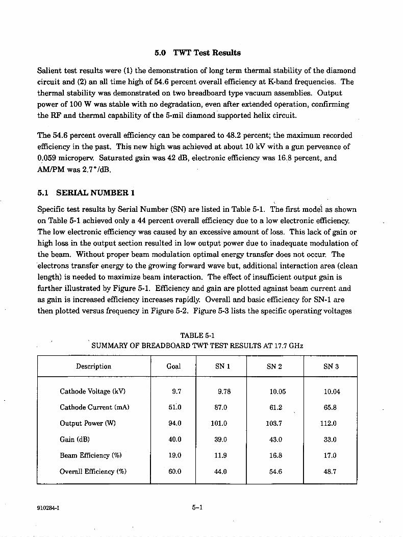
5.0 TWT Test Results
Salient test results were (1) the demonstration of long term thermal stability of the diamondcircuit and (2) an all time high of 54.6 percent overall efficiency at K-band frequencies. Thethermal stability was demonstrated on two breadboard type vacuum assemblies. Outputpower of 100 W was stable with no degradation, even after extended operation, confirmingthe RF and thermal capability of the 5-mil diamond supported helix circuit.
The 54.6 percent overall efficiency can be compared to 48.2 percent; the maximum recordedefficiency in the past. This new high was achieved at about 10 kV with a gun perveance of0.059 microperv. Saturated gain was 42 dB, electronic efficiency was 16.8 percent, andAM/PM was 2.7°/dB.
5.1 SERIAL NUMBER 1\
Specific test results by Serial Number (SN) are listed in Table 5-1. The first model as shownon Table 5-1 achieved only a 44 percent overall efficiency due to a low electronic efficiency.The low electronic efficiency was caused by an excessive amount of loss. This lack of gain orhigh loss in the output section resulted in low output power due to inadequate modulation ofthe beam. Without proper beam modulation optimal energy transfer does not occur. Theelectrons transfer energy to the growing forward wave but, additional interaction area (cleanlength) is needed to maximize beam interaction. The effect of insufficient output gain isfurther illustrated by Figure 5-1. Efficiency and gain are plotted against beam current andas gain is increased efficiency increases rapidly. Overall and basic efficiency for SN-1 arethen plotted versus frequency in Figure 5-2. Figure 5-3 lists the specific operating voltages
TABLE 5-1SUMMARY OF BREADBOARD TWT TEST RESULTS AT 17.7 GHz
Description
Cathode Voltage (kV)
Cathode Current (mA)
Output Power (W)
Gain (dB)
Beam Efficiency (%)
Overall Efficiency (%)
Goal
9.7
51.0
94.0
40.0
19.0
60.0
SN1
9.78
87.0
101.0
39.0
11.9
44.0
SN2
10.05
61.2
103.7
43.0
16.8
54.6
SN3
10.04
65.8
112.0
33.0
17.0
48.7
910284-1 5-1
12
10
I647
UJ
gLL.U.Ill
50
BASIC EFFICIENCY
SATURATED GAIN
60 70
BEAM CURRENT (mA)
80
EK
EA
f
-9700V
VARIED
19 GHz
90
40
35
30
25
Figure 5-1 953H Breadboard TWT SN-1 effect of insufficient output gain.
501648
40
g. 30
o
UJ20
10
OVERALL EFFICIENCY
BASIC EFFICIENCY
EK = 9780 kV
IK = 86.7 mA
17 18 19
FREQUENCY (GHz)
20 21
Figure 5-2 953H Breadboard TWT SN-1.
5-2 910284-1
50
cctii49
48
41
CDT3
40
39
EK = -9780 VIK = 86.7 mA
I
100 ft
90 IccUJ
EK
EA
75
b3
-9780 V IK
+ 4100V IA
-5520 V IB1
-7030V IK
-8840V IM
-9780 V IM
I649
86.7mA
0.009mA
24.5 mA
23.1 mA
37.3 mA
0.0mA
1.8mA
17.7 19.0FREQUENCY (GHz)
20.2
Figure 5-3 953H TWT SN1 output power and gain characteristics.
and currents next to a plot of saturated output power and saturated gain. SN-1 achieved100 W of output power and was operated at this power level for an extended period of time"with no degradation.
SN-l's test performance can be summarized as follows:
• Good beam transmission
• Stable BWO free operation
• Thermal and RF stability in a diamond circuit at 100 watts CW power output
• 75 watts CW power across desired frequency band
• Output circuit section required more gain to boost efficiency
• Highest overall efficiency achieved was 44 percent
5.2 SERIAL NUMBER 2
The significant change from SN-1 to SN-2 was an increase in the clean length. As is evidentfrom Table 5-1 and Figure 5-4, both the electronic efficiency and the overall efficiency
910284-1 5-3
165070
60
50
40
g 30
20
10
IK =
10 kV
60.7mA
OVERALL EFFICIENCY
BASIC EFFICIENCY
17 18 19
FREQUENCY (GHz)
20 21
Figure 5-4 953H TWT SN-2 efficiency characteristics.
improved considerably. The operating voltages and currents for SN-2 are found inFigure 5-5. From the plot of saturated power and gain versus frequency. It is evident thatthe highest efficiency is at 17.7 GHz. A reduction in the shield diameter for SN-3 wouldhave centered performance. However, a new output helix was already being incorporatedand in order to clearly evaluate the new DVT design it was decided not to introduce othervariables.
The overall efficiency achieved was exceptional for SN-2 but the 60 percent goal was notmet. The design process was reviewed and an error in the DVT model was isolated. Afterthe computer model was revised the DVT program predictions closely correlate with SN-2'smeasured performance. To ascertain the optimum output clean length, electronic efficiencyversus beam current was also taken on SN-2. From the data in Figure 5-6 it was concludedthat additional clean length was needed to maximize the basic efficiency.
SN-2's test performance can be summarized as follows: '
• Good beam transmission
" • Thermal and RF stability of diamond circuit at 104 watts CW power
• Highest power and efficiency at 17.7 GHz (tube band centered low)
5-4 910284-1
1651
DCUl
52
50
48
46
50
2. 40
30
2017 18 19
FREQUENCY (GHz)
20
EK = -10 kV
EA = 270V
Eb1 = -5930V
ESZ = -7100V
EM = -8440 V
EM = -9780V
IK = 60.7 mA
IA = 0.002 mA
Ib1 = 17.7mA
Ib2 = 26.4 mA
'b3 = 16-0 mA
Ib4 = 0.0 mA
lw = 1.0mA
21
Figure 5-5 953H TWT SN-2 output power and gain characteristics.
• High small signal gain ripple (output attenuator pattern too abrupt)
• Circuit efficiency increased further by increasing output gain
• Highest efficiency achieved was 54.6 percent
5.3 SERIAL NUMBER 3
Using the improved DVT model, SN-3's helix design was then optimized and should havereached 20 percent electronic efficiency. SN-3, however, resulted in 17 percent electronicefficiency, as is illustrated in Figure 5-7 where efficiency is plotted versus frequency.Oscillations in the output circuit also were present at small signals which made the evalua-tion more difficult. The oscillations were caused by an excessive amount of clean length, aresult of circuit rework. Details regarding the operating voltages and currents for SN-3 arefound in Figure 5-8 along with a plot of saturated power and gain.
SN-3 had low resistance between the second and third stage electrodes, approximately 6Mii. The collector was X-rayed in efforts to ascertain the problem, but the resolution waspoor and no conclusions could be made. In preparing SN-2 for shipment to NASA, it wasdiscovered that the previously low current leakage recorded in the collector had increased toSN-3's level. The leakage was definitely not there from when SN-2 was being tested. SN-1
910284-1 5-5
1652
UJ
O
O
18
16
14
12
10
EK
EA
F
-10 kV
VARIED
17.7 GHz
OPERATING CATHODECURRENT = 60.7 mA
30
50
40
30
UJ
g£ 20
10
40 50 60 70
BEAM CURRENT (mA)
Figure 5-6 953H TWT SN-2 basic efficiency versus beam current:
I653
OVERALL EFFICIENCY
EK = 10 kV
IK = 65 mA
BASIC EFFICIENCY
17 18 19 20 21
FREQUENCY (GHz)
Figure 5-7 953H TWT SN-3 efficiency characteristics.
5-6 910284-1
1654
2-oc
-
o
60
58
X
54
52
50
48
46
44
42
40
*36
34
32
30
28
EK = 10.000V
EA = 110V
Eb1 = -4825 V
EK, = -5167 V
EM = -7694 V
EM = -9780 V
IK = 65.0 mA
IA = 0.03 mA
lbt = 36.6 mA
Ib2 = 4.5mA
IM = 21.9mA
IM = 0.0mA
lw = 1.49mA
17 18
FREQUENCY (GHz)
19 20 21
Figure 5-8 953H TWT SN-3 output power and gain characteristics.
was also retested but no change in the leakage current was detected. Whether it is signifi-cant that both SN-2 and SN-3 had textured electrodes is not known. However, there isconcern with the spires possibly breaking or collapsing and forming a leakage path.
In conclusion, SN-3's performance can be summarized as follows:
• Good beam transmission
• Thermal stability of diamond circuit at 112 watts CW power
• 75 watts CW power across desired frequency band
• Highest electronic efficiency was 17 percent
• Low overall gain (input gain too low)
• Output unstable at small signal (output gain too high)
• High leakage current (6 mA) after bakeout between third and fourth collectorstages affected overall efficiency
• Highest efficiency achieved was 48.7 percent
910284-1 5-7
6.0 CONCLUSIONS AND RECOMMENDATIONS
6.1 CONCLUSIONS
The 953H TWT achieved an overall efficiency of 54.6 percent, which is a new benchmark inTWT technology for K-band devices. This high efficiency was obtained by utilizing state-of-the-art technologies. Technology areas included circuit design (Dynamic Velocity Tapers),materials (diamond, graphite, dispersion hardened copper), processes (electron beamsputtering), new assembly techniques (cold compression circuits), and highly improved finiteelement analyses (mechanical, thermal, and electrical). These technologies were integratedinto a single TWT design for the first time under this program.
Manufacturing techniques developed have significantly advanced diamond rod technology. Anewly developed cold compression technique for assembling the helix circuit replaced heatshrinking and the eliminated high temperatures associated with the process. This helixdesign demonstrated excellent thermal capabilities by handling in excess of 100 watts of CWpower, at 20 GHz. This technique has not only proven successful in eliminating power fadeproblems experienced in the past, but will also open the door to other helix support materialthat can only be manufactured in small segments.
To further illustrate the accomplishments of this program, Table 6-1 shows a comparison ofsimilar K-band TWTs and the efficiency improvements that have occurred due to recentTWT technology advancements. The first column lists results for a K-band TWT withuniform helix pitch and beryllia support rods. In the second column, incorporation of theDynamic Velocity Tapered (DVT) helix improved beam conversion efficiency by almost5 percent (from 7.3 to 12.2 percent). The third column, an additional 4.7 percent (from 12.2to 16.9 percent) has been gained using diamond support rods. Overall efficiency alsoinfluenced by the collector design improved substantially in each case.
6.2 RECOMMENDATIONS
Additional units should be built to determine the true performance capabilities of SN-3'sconfiguration. SN-3's exponential tapered helix produced a higher basic efficiency thanSN-2's linear tapered design, thus overall efficiency for the final configuration should behigher than 54.6 percent. The leakage current in the SN-3's collector prevented verificationof the overall efficiency.
Considering the exorbitant cost of segmented diamond support rods, other types of materialsshould be investigated to support the helix. Possibilities include cubic boron nitride,Beramic Z, or possibly, utilization of diamond deposition to form a long hollow rod.
910284-1 6-1
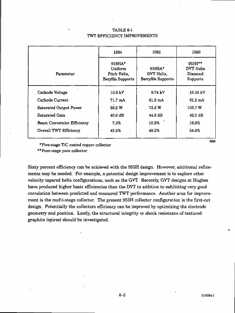
TABLE 6-1TWT EFFICIENCY IMPROVEMENTS
Parameter
Cathode Voltage
Cathode Current
Saturated Output Power
Saturated Gain
Beam Conversion Efficiency
Overall TWT Efficiency
1984
918HA*Uniform
Pitch Helix,Beryllia Supports
10.8 kV
71.7mA
56.2 W
40.0 dB
7.3%
42.5%
1985
918HA*DVT Helix,
Berryllia Supports
9.74 kV
61.9mA
73.3 W
44.6 dB
12.2%
48.2%
1986
953H**DVT HelixDiamondSupports
10.05 kV
61.2mA
103.7 W
42.0 dB
16.9%
54.6%
* Five-stage TiC coated copper collector** Four-stage poco collector
1656
Sixty percent efficiency can be achieved with the 953H design. However, additional refine-ments may be needed. For example, a potential design improvement is to explore othervelocity tapered helix configurations, such as the GVT. Recently, GVT designs at Hugheshave produced higher basic efficiencies than the DVT in addition to exhibiting very goodcorrelation between predicted and measured TWT performance. Another area for improve-ment is the multi-stage collector. The present 953H collector configuration is the first-cutdesign. Potentially the collectors efficiency can be improved by optimizing the electrodegeometry and position. Lastly, the structural integrity or shock resistance of texturedgraphite (spires) should be investigated.
6-2 910284-1
APPENDIX A
953H TRAVELING-WAVE TUBE
DIAMOND CIRCUIT MECHANICAL ANALYSIS
910284-1 A-l
953H TRAVELING-WAVE TUBEDIAMOND CIRCUIT
MECHANICAL ANALYSIS
CONTRACT NO. NAS3-24897
NOVEMBER 1988
PREPARED BY:
APPROVED BY:
APPROVED BY:
?-7-<S5
K. A. NORENBERGMEMBER OF THE TECHNICAL STAFFMECHANICAL ENGINEERING
M. FILLER ''PROJECT MANAGERMECHANICAL ENGINEERING
DATE
DATE .
R. N. TAMASHIROPROGRAM MANAGERSPACE TUBE AND DEVELOPMENT DEPARTMENT
DATE
HUGHES AIRCRAFT COMPANYELECTRON DYNAMICS DIVISION3100 WEST LOMITA BOULEVARD
P.O. BOX 2999TORRANCE, CA 90509-2999

Page Intentionally Left Blank

TABLE OF CONTENTS
Section Page
1.0 INTRODUCTION 1
2.0 STRUCTURAL ANALYSIS 5
2.1 Coining Operation 102.2 Bakeout Process 122.3 Initial Operating Condition 13
3.0 THERMAL ANALYSIS 17
4.0 LONG-TERM OPERATION 27
5.0 CONCLUSION 35
6.0 REFERENCES 37
111
LIST OF ILLUSTRATIONS
Figure Page
1 Cross section of 953H output circuit (top view). 2
2 Cross section of 953H output circuit (axial view). 3
3 2-D finite element model of the 953H output circuit. 6
4 Close-up of the helix/rod interface. 7
5 Close-up of the rod/sleeve interface. 8
6 Thermal interface coefficients. 14
7 Cross section (top view) of the 3-D finite element model of theoutput circuit. 18
8 Heatsink design. 20
9 Power distribution for thermal analysis. 22
10 Temperature distribution through cross section at end of rods(copper sleeve case). 23
11 Temperature distribution through cross section at end of rods^ (GlidCop sleeve case). 25
12 Temperature distribution through cross section at end of rods .(copper sleeve case) for end-of-life condition. 30
13 Temperature distribution through cross section at peak helixtemperature (GlidCop sleeve case) for end-of-life condition. 33
PRECEDING PAGE BLANK NOT FILMED
LIST OF TABLES
Table Page
1 Material Properties Used in Structural Analysis 9
2 Results of Coining Analysis 11
3 Results of Bakeout Analysis (Room Temperature) 13
4 Results of Structural Analysis (Operation) 16
5 Thermal Conductivities 19
6 Temperature Distribution For Copper Sleeve Case (°C) 24
7 Temperature Distribution for Glidcop Sleeve Case (°C) 24
8 Secondary Creep Strain Rates 28
9 Interface Values for End-Of-Life Estimate (Copper Sleeve) 29
10 Temperature Distribution for End-Of-Life With Copper Sleeve (°C) 31
11 Interface Values For End-Of-Life Condition (Glidcop Sleeve) 32
12 Temperature Distribution For End-Of-Life With Glidcop Sleeve (°C) 34
VIIPRECEDING PAGE BLANK NOT FILMED
1.0 INTRODUCTION
The design of the output circuit of the 953H TWT is distinguished from others by the use ofdiamond support rods. This output circuit will be assembled by a coining technique, a rela-tively new alternative to the heatshrink assembly process. A combined structural and ther-mal analysis has been performed to investigate the fabrication procedure and to determinethe temperature distribution in the output circuit during operation. The predicted tempera-tures are used to judge the ability of the design to handle the required thermal loads. Theprimary design limit requires that the peak helix temperature must be below 300 °C. Thiscriterion is very conservative and was chosen to ensure good electrical performance of thecircuit.
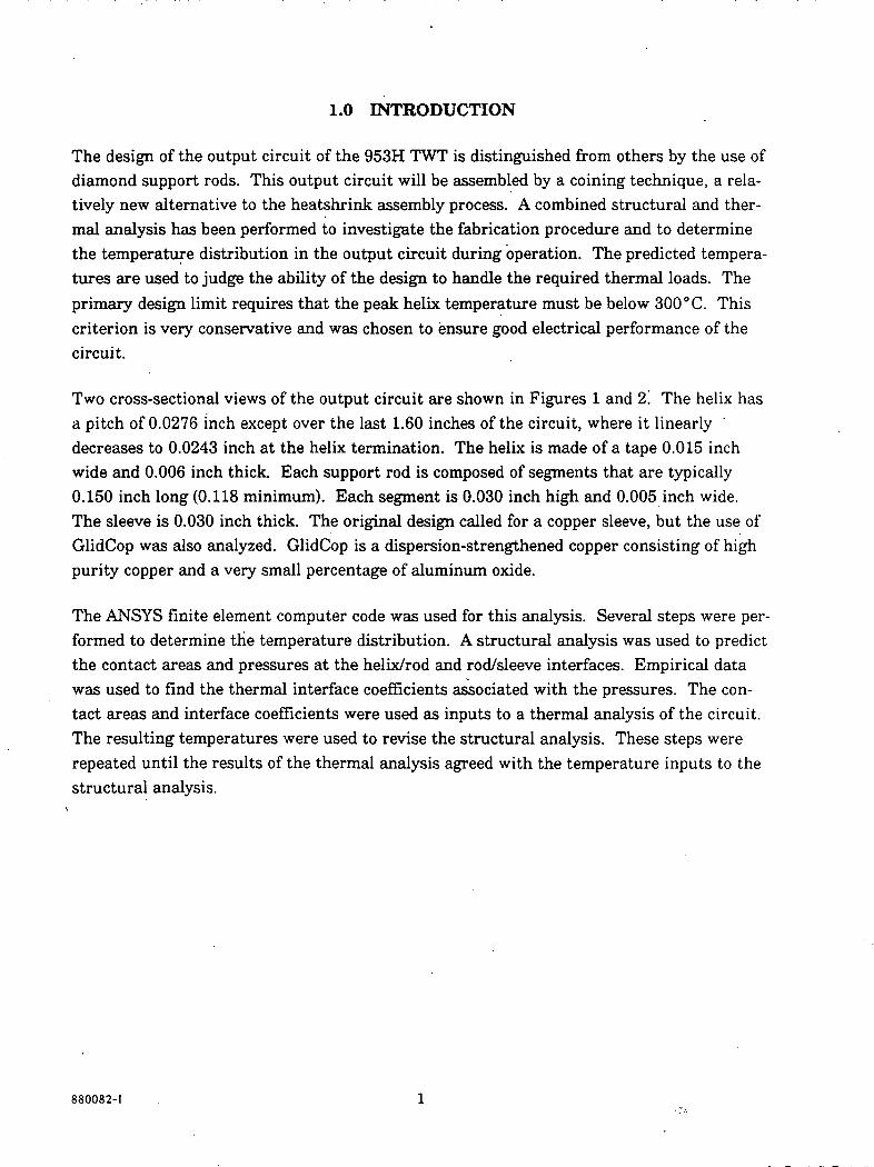
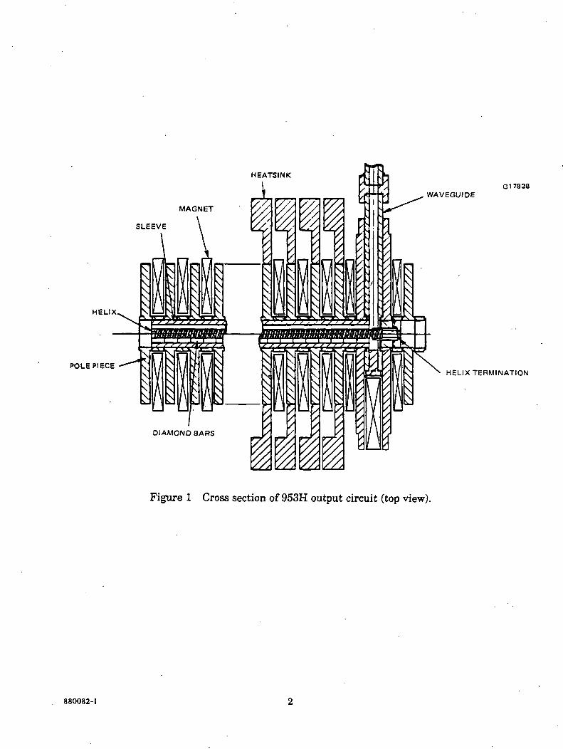
Two cross-sectional views of the output circuit are shown in Figures 1 and 2. The helix hasa pitch of 0.0276 inch except over the last 1.60 inches of the circuit, where it linearlydecreases to 0.0243 inch at the helix termination. The helix is made of a tape 0.015 inchwide and 0.006 inch thick. Each support rod is composed of segments that are typically0.150 inch long (0.118 minimum). Each segment is 0.030 inch high and 0.005 inch wide.The sleeve is 0.030 inch thick. The original design called for a copper sleeve, but the use ofGlidCop was also analyzed. GlidCop is a dispersion-strengthened copper consisting of highpurity copper and a very small percentage of aluminum oxide.
The ANSYS finite element computer code was used for this analysis. Several steps were per-formed to determine the temperature distribution. A structural analysis was used to predictthe contact areas and pressures at the helix/rod and rod/sleeve interfaces. Empirical datawas used to find the thermal interface coefficients associated with the pressures. The con-tact areas and interface coefficients were used as inputs to a thermal analysis of the circuit.The resulting temperatures were used to revise the structural analysis. These steps wererepeated until the results of the thermal analysis agreed with the temperature inputs to thestructural analysis.
880082-1
HEATSINK
MAGNET
SLEEVE
HELIX
POLE PIECE
G17838WAVEGUIDE
HELIX TERMINATION
Figure 1 Cross section of 953H output circuit (top view).
880082-1
NOTE: DRAWING IS NOT TO SCALE.
G17839
DIAMOND SUPPORT ROD (3)
TUNGSTEN/3% RHENIUMTAPE HELIX
BARREL(IRON POLE PIECE/MONEL SPACER)
SLEEVE(COPPER OR GLIDCOP)
Figure 2 Cross section of 953H output circuit (axial view).
880082-I
2.0 STRUCTURAL ANALYSIS
The first phase of the structural analysis was the investigation of the coining procedure.The next phase began with the analysis of the bakeout process during which the vacuumassembly is held at 500 °C for two to three days. This was followed by an analysis of theinitial operating condition.
The physical phenomena associated with coining, bakeout, and operation are very compli-cated and would be best simulated with a three-dimensional (3-D) finite element model.However, this was not feasible because of the limitation of the computing resources availableat HEDD. Therefore, a two-dimensional (2-D) model was used for all phases of the struc-tural analysis (Figure 3). The model consists of 634 nodes and 565 elements. Close-ups ofthe helix/rod and rod/sleeve interfaces are shown in Figures 4 and 5. A 60-degree slice withtangential constraints on the edges was modeled to take advantage of the symmetry of theassembly. (The treatment of the asymmetry of the helix is discussed in later sections.) Thesesymmetry boundary conditions have the effect of preventing slippage at the interfaces. Thisconstraint is reasonable since the rod is expected to grab and dig into the helix coating andsleeve. The copper coating on the helix was assumed to be 0.0003 inch thick. The barrelwas represented by a combination of electrolytic iron and Monel 404 with an outer diameterapproximately the same size as that of the spacer. The gold plating on the outer diameter ofthe sleeve was not treated as a separate material.
The finite element formulations used in this analysis are based on small strain and small dis-placement conditions. The von Mises yield criterion and the Prandtl-Reuss flow equationswere used to govern plasticity. Bilinear stress-strain curves were used for the metallic com-ponents. Initially, the kinematic hardening rule was used for all of the metals. However, itbecame necessary to switch to the isotropic hardening rule for the sleeve and helix coatingduring the coining analysis. This is further discussed in the next section. The initial stressmethod was used to solve the nonlinear equations associated with plasticity. This methodinvolves iterative modification of the load vector while the stiffness matrix remainsunchanged.1
The material properties used in the structural analysis are given in Table 1. The propertiesfor pure tungsten were used for the tungsten alloy. The thermal expansion coefficient forGlidCop was taken as the average of reported data and assumed to be constant with tem-perature. The temperature-dependence of the GlidCop stress-strain curve was assumed to bethe same as that of copper. The ratios between the tangent modulus and elastic modulus forthe metals were chosen to correspond to approximately 5 percent strain.
880082-1 PRECEDE PAGE BUNK NOI
G17840
BARREL
SYMMETRYPLANE
HELIX
SLEEVE
SYMMETRY PLANE
Figure 3 2-D finite element model of the 953H output circuit.
880082-I
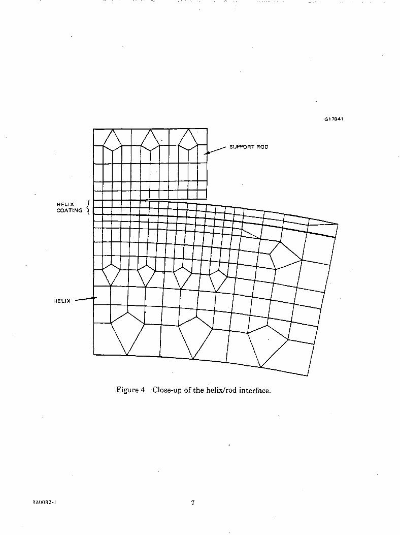
G17841
SUPPORT ROD
HELIXCOATING
HELIX
Figure 4 Close-up of the helix/rod interface.
880082-I
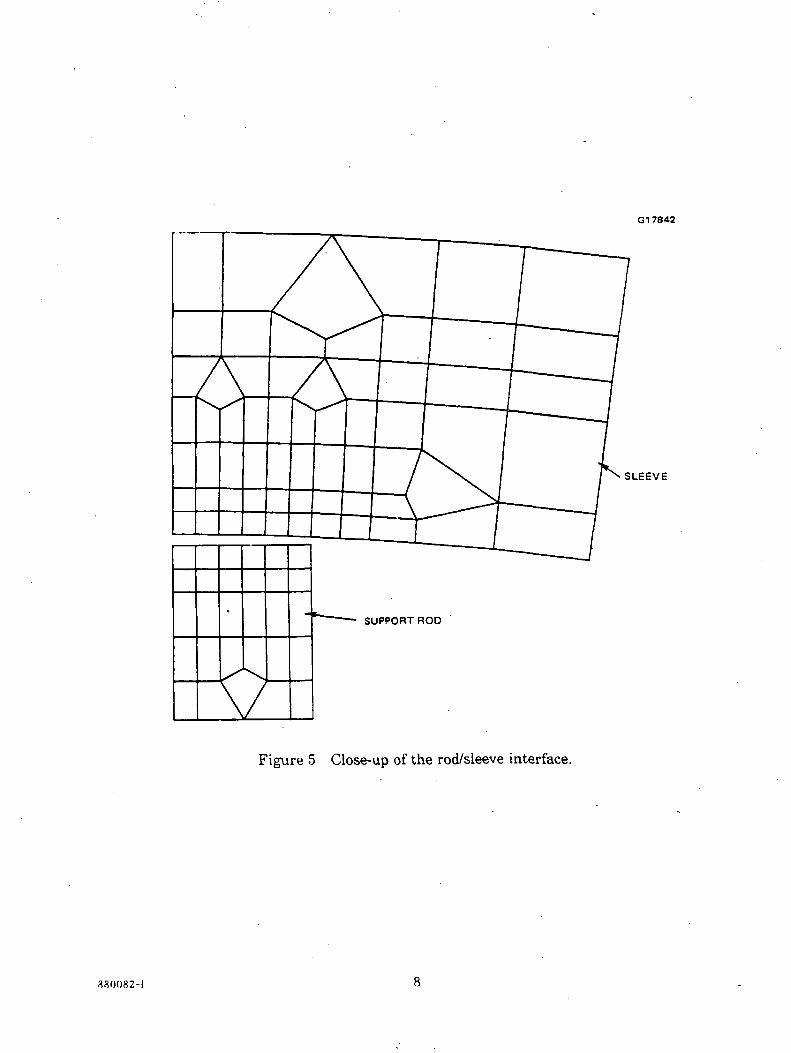
G17842
SLEEVE
Figure 5 Close-up of the rod/sleeve interface.
380082-I
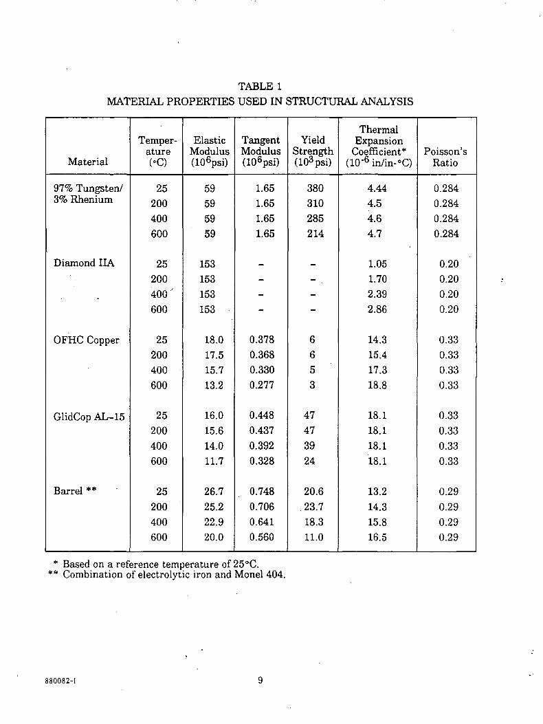
TABLE 1MATERIAL PROPERTIES USED IN STRUCTURAL ANALYSIS
Material
97% Tungsten/3% Rhenium
Diamond IIA
OFHC Copper
GlidCop AL-15
Barrel **
Temper-ature(°C)
25200400600
25200400'600
25200400600
25200400600
25200400600
ElasticModulus(106psi)
59595959
153153153153
18.017.515.713.2
16.015.614.011.7
26.725.222.920.0
TangentModulus(106psi)
1.651.651.651.65
_
—
-
0.3780.3680.3300.277
0.4480.4370.3920.328
0.7480.7060.6410.560
YieldStrength(103psi)
380310285214
_
—
-
6653
47473924
20.623.718.311.0
ThermalExpansion
Coefficient*(10 -6 in/in- °C)
4.444.54.64.7
1.051.702.392.86
14.315.417.318.8
18.118.118.118.1
13.214.315.816.5
Poisson'sRatio
0.2840.2840.2840.284
0.200.200.200.20
0.330.330.330.33
0.330.330.330.33
0.290.290.290.29
* Based on a reference temperature of 25 °C.** Combination of electrolytic iron and Monel 404.
880082-1
2.1 COINING OPERATION
The coining operation is the process by which the helix/rod and rod/sleeve interfaces are putinto compression. The helix and support rods are first inserted into the sleeve. The sleeve isthen placed in the die and compressed with a force of approximately 20 tons.
The 2-D plane strain assumption was used for the analysis of the coining operation. Thiscaused the axial motion of the elements to be constrained in the out-of-plane (axial) direc-tion. This assumption is reasonable because the friction between the die and the sleeveshould tend to restrain the axial motion. One disadvantage of using a 2-D model is that itrepresented the helix as a hollow cylinder. In an attempt to account for the 3-D effect of thehelix, the resultant rod/sleeve contact pressures were scaled by one half. This was based ona helix width of 0.015 inch and an initial pitch estimate of 0.030 .inch.
At this stage of the analysis, the sleeve was assumed to be made of copper. Preliminarycoining experiments indicated that the load imposed by the die was essentially axisymmetric.Since the die is very stiff in comparison to the sleeve, the loading was treated in the analysisas a uniform enforced radial displacement at the outer diameter of the sleeve. The nodes inthe model representing the outer diameter were connected to dummy nodes by interface(gap) elements. These elements act as stiff radial springs in compression, but carry essen-tially no load in tension. The loading by the die was implemented by incrementally increas-ing enforced displacements on the dummy nodes up to a final value of 0.00105 inch. Thisincremental approach was necessary because of the use of nonlinear stress-strain curves forthe metallic components. Plasticity is a nonconservative phenomenon that requires a rea-sonably accurate description of the load history. During unloading, the enforced displace-ments were incrementally decreased until the compression was removed from all of the inter-face elements. At this point, the model represented the coined assembly after removal fromthe die.
Gap elements were also used between the pairs of nodes at the component interfaces. Theresultant contact areas were found by determining which gaps had closed. The compressiveloads carried by the individual gap elements were summed to determine the total interfaceforces. The reported contact pressures represent average values for each interface.
The kinematic hardening rule was used for the metallic components in a preliminary analy-sis of the coining operation. During the loading phase of the coining, very large plasticstrains developed in the helix coating and sleeve. The tangent modulus of copper decreases agreat deal as the strain increases, so the use of a bilinear stress-strain curve led to resultsthat underestimated the strain and overestimated the stress. Although the use of a lowertangent modulus was considered, it was rejected because of the difficulty in reaching a
880082-1 10
converged solution. Since the stress was well above twice the yield strength in many ele-ments, the use of the kinematic hardening rule led to a prediction of additional plastic strainupon unloading. The resultant interface force was also unreasonably low. These resultswere not considered to be physically realistic, so a switch was made to isotropic hardening inthe coating and sleeve for unloading. This prevented the development of additional plasticstrain and led to a more reasonable final solution. Since the actual hardening behavior ofmost metals falls between the kinematic and isotropic assumptions, the use of either can bejustified. The advantage of the kinematic hardening rule in ANSYS is that it can accountfor the temperature-dependence of all the material properties. With isotropic hardening, theyield strength and tangent modulus are assumed to be constant with temperature. Thislimitation was considered acceptable since most of the important physical phenomena occurbelow 300 °C and the values for copper vary by less than 10 percent over this range.
The results of the final coining analysis are given in Table 2. The helix/rod contact area isreported in square inches for each contact point. The maximum possible contact area is7.5 x 10~5 in2 (based on a 0.005-inch rod width and a 0.015-inch helix tape width). Thereported values are conservative because the high localized plastic strains that occur duringthe coining process are not fully developed in this finite element analysis. The rod/sleevecontact area is reported in square inches per inch of length of each rod. Even with theconservative nature of this analysis, the reported values are at the maximum possible,5.0 x 10"3 in2 /in. The interface force is given in terms of pounds per inch of length of eachrod.
TABLE 2RESULTS OF COINING ANALYSIS
Quantity
Helix/rod contact area(in2 /contact point)
Helix/rod pressure (ksi)
Rod/sleeve contact area(in2 /in/rod)
Rod/sleeve pressure (ksi)
Interface force(Ibs/in/rod)
Under Full LoadFrom Die
5.1 xlO'5
194
5.0x10⁻³
66
329
RemovedFrom Die
2.4xlO" 5
115
5.0x10⁻³
18
92
880082-1 11
2.2 BAKEOUT PROCESS
In the bakeout process the vacuum assembly is slowly raised from room temperature to500 °C, held there for two to three days, then slowly brought back to room temperature.Since this loading causes thermal expansion, the constrained axial motion of the plane strainassumption is inappropriate. Therefore, the 2-D plane stress assumption, in which axialmotion is unrestrained, was required for the bakeout analysis. An attempt was made to ana-lyze the bakeout process as a continuation of the coining analysis by switching assumptionsmidstream, but the results were unrealistic and unacceptable. This difficulty arose from thelimitation of using a 2-D model to describe all of the physical phenomena associated withthe manufacture and operation of the output circuit. In addition, the inability of ANSYS toadequately handle the extremely high plastic strains developed in the coining process isresponsible for additional inaccuracy in the subsequent load steps.
In light of this development, the best alternative was to treat the bakeout process as thebeginning of a separate analysis. The assembly was assumed to begin stress-free at 500 °Cwith the interfaces barely in contact. This was considered to be a reasonable starting pointbecause of the high creep rate of the copper sleeve and coating. Holding the assembly at500 °C for two to three days should be sufficient to cause the stresses to be very low through-out. The disadvantage of this approach is that it does not account for the flat indentationsin the helix coating and sleeve caused by the rods during coining. As a result, the predictedinterface areas are probably smaller than the actual areas.
The cooldown to room temperature was simulated by applying uniform temperatures in suc-cessive load steps: 450, 400, 325, 250, 175, 100, and 25°C. The temperature gradientswithin the assembly were ignored because the actual cooling is very slow.
After the completion of the coining analysis, an improvement in the analytical technique wasdeveloped. It was found that the 3-D effect could be better represented by modifying thestiffness of the helix. With a helix tape width of 0.015 inch and a pitch of 0.030 inch, thehelix should behave as if it is half as stiff as a continuous tube. Therefore, the stress-straincurves for the helix and helix coating materials were scaled down by one half. This changewas incorporated into the bakeout analysis. As before, the isotropic hardening rule was usedfor the helix coating and sleeve while kinematic hardening was used for the helix and barrel.
After analyzing the original design with a copper sleeve, the use of GlidCop as the sleeve ma-terial was considered. GlidCop has a much higher yield point than copper and a much lowercreep strain rate. These facts suggested that its use would improve the design because theinterface forces during operation would be higher and they would be maintained better overa long period of time. The previously mentioned assumptions were also used for the analysis
880082-1 12
of the GlidCop sleeve. However, the stress-free initial condition is not as good in this casebecause of the low creep rate for the sleeve. This assumption makes the analysis more con-servative because the interface forces at 500 °C are probably quite significant:
The results of the bakeout analysis are given in Table 3. The values represent the conditionof the output circuit at room temperature. The use of the GlidCop sleeve results in a muchhigher interface force, which is responsible for the larger contact area at the helix/rod inter-face. Despite the higher force, the rod/sleeve contact area with the GlidCop sleeve is belowthe maximum value. This conflicts with a destructive physical analysis of a thermal test cir-cuit that showed that full contact existed at room temperature. This discrepancy is mostlikely attributable to the inability to account for the strain history of the sleeve in the coin-ing process.
2.3 INITIAL OPERATING CONDITION
The analysis of the initial operating condition continued from the bakeout analysis. Esti-mates of the expected operating temperatures were used as loads to the model. To assureproper treatment of the change in load direction, two load steps were used to reach the finaltemperatures. The applied temperatures were uniform over each component. This was rea-sonable since the radial temperature gradient within each component should be small. Thecopper sleeve and GlidCop sleeve cases were both considered.
TABLESRESULTS OF BAKEOUT ANALYSIS
(ROOM TEMPERATURE)
Quantity
Helix/rod contact area(in2 /contact point)
Helix/rod pressure (ksi)
Rod/sleeve contact area(in^ /in/rod)
Rod/sleeve pressure (ksi)
Interface force(Ibs/in/rod)
With CopperSleeve
S.lxlO'5
72
5.0 x 10'3
25
123
With GlidCopSleeve
6.6 xlO'5
119
3.4 x 10'3
77
263
880082-1 13
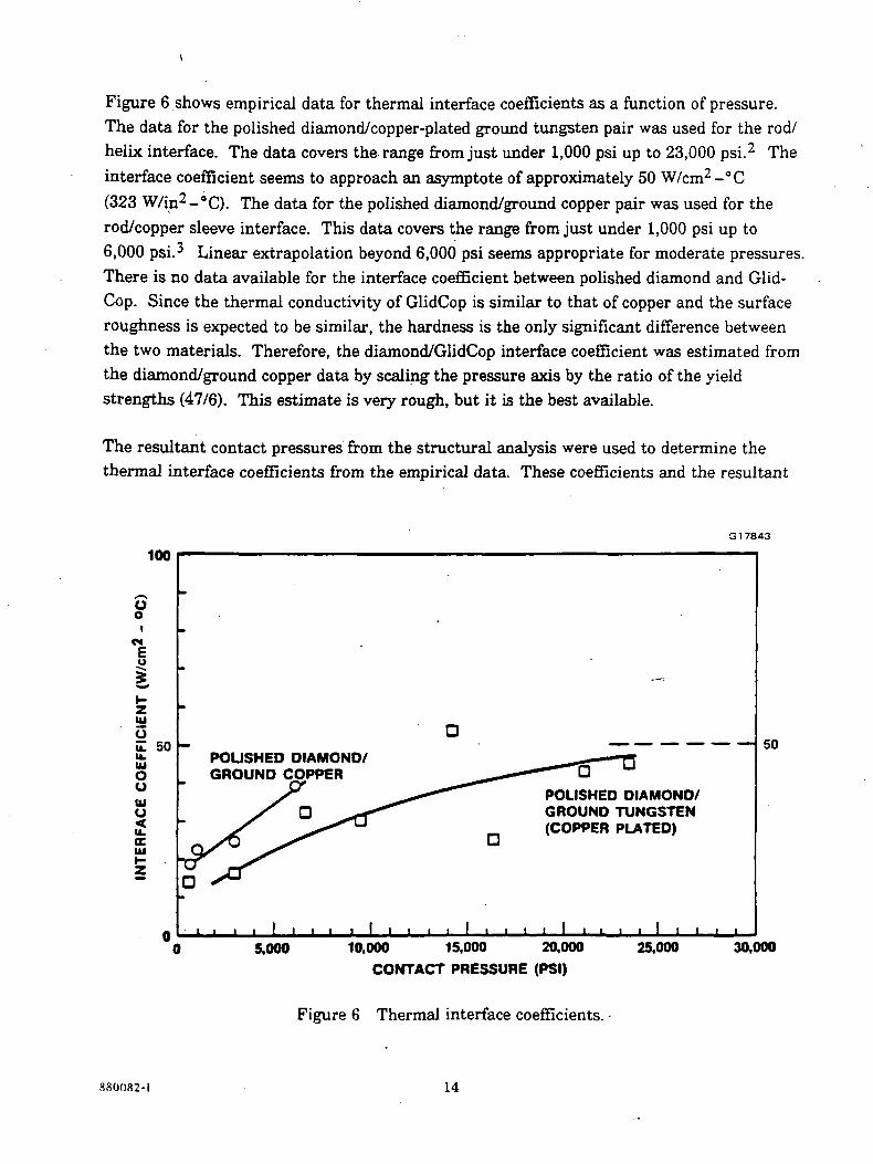
Figure 6 shows empirical data for thermal interface coefficients as a function of pressure.The data for the polished diamond/copper-plated ground tungsten pair was used for the rod/helix interface. The data covers the range from just under 1,000 psi up to 23,000 psi.2 Theinterface coefficient seems to approach an asymptote of approximately 50 W/cm2-°C
(323 W/in2-8C). The data for the polished diamond/ground copper pair was used for therod/copper sleeve interface. This data covers the range from just under 1,000 psi up to6,000 psi.3 Linear extrapolation beyond 6,000 psi seems appropriate for moderate pressures.There is no data available for the interface coefficient between polished diamond and Glid-Cop. Since the thermal conductivity of GlidCop is similar to that of copper and the surfaceroughness is expected to be similar, the hardness is the only significant difference betweenthe two materials. Therefore, the diamond/GlidCop interface coefficient was estimated fromthe diamond/ground copper data by scaling the pressure axis by the ratio of the yieldstrengths (47/6). This estimate is very rough, but it is the best available.
The resultant contact pressures from the structural analysis were used to determine thethermal interface coefficients from the empirical data. These coefficients and the resultant
317843
100
uo
M
U
UioE 50ikUJOUUJU<IkIT
POLISHED DIAMOND/GROUND COPPER
POLISHED DIAMOND/GROUND TUNGSTEN(COPPER PLATED)
I I5,000 10,000 15,000 20,000
CONTACT PRESSURE (PSI)
Figure 6 Thermal interface coefficients.
25,000
50
30,000
880082-I 14
contact areas from the analysis were used as inputs to the thermal analysis (see Section 3.0).The resultant temperatures were then applied to the structural model again (starting fromthe point representing the end of bakeout, 25°C). This iterative process was repeated untilthe temperatures from the thermal analysis were consistent with the pressures and areasfrom the structural analysis.
The peak helix temperature occurs near the end. of the rods for both the copper sleeve andGlidCop sleeve cases. Therefore, the component temperatures at the cross section at the endof the rods were chosen as the inputs to the structural runs. The inputs and results for theconverged cases are given in Table 4. The derivation of the temperature inputs is describedmore fully in Section 3.0. The results show that a greater portion of the interface force ismaintained when the GlidCop sleeve is used. This causes the contact area and pressure atthe helix/rod interface to be much higher than in the copper sleeve case. In both cases, theasymptotic limit was used for the thermal interface coefficient. At the rod/sleeve interface,the contact area remained at the maximum value for the copper sleeve. However, the areafor the GlidCop sleeve decreased slightly from the room temperature value. Although therod/sleeve pressure is much higher with the GlidCop sleeve than with the copper sleeve, theinterface coefficient is slightly lower.
880082-1 15
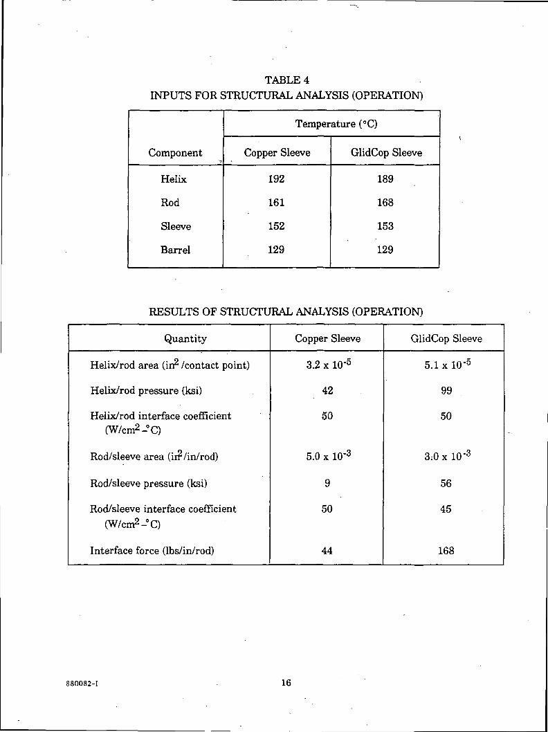
TABLE 4INPUTS FOR STRUCTURAL ANALYSIS (OPERATION)
Component
Helix
Rod
Sleeve
Barrel
Temperature (°C)
Copper Sleeve
192
161
152
129
GlidCop Sleeve
189
168
153
129
RESULTS OF STRUCTURAL ANALYSIS (OPERATION)
Quantity
Helix/rod area (in2 /contact point)
Helix/rod pressure (ksi)
Helix/rod interface coefficient(W/cm2-C)
Rod/sleeve area (ir? /in/rod)
Rod/sleeve pressure (ksi)
Rod/sleeve interface coefficient(W/cm2-C)
Interface force (Ibs/in/rod)
Copper Sleeve
3.2 x 10'5
42
50
5.0 x 10'3
9
50
44
GlidCop Sleeve
5.1 x 10'5
99
50
3.-0 x 10 '3
56
45
168
880082-1 16
3.0 THERMAL ANALYSIS
A 3-D finite element model was used for the thermal analysis of the output circuit. Thiswas necessary because of the asymmetry of the design and the importance of the axial com-ponent of heat transfer. The use of a 3-D model was practical because the thermal analysisdid not require the same level of detail as the structural analysis. The thermal analysis wascarried out for both the copper sleeve and GlidCop sleeve cases.
A cross section (top view) of the model is shown in Figure 7. The TWT is modeled from thecollector face to a point approximately 2.4 inches from the helix termination. The modelconsists of 4278 nodes and 3724 elements. The thermal conductivities of the materials usedin the analysis are shown in Table 5. The helix was modeled with thermal bars that weregiven an equivalent conductivity to account for the copper coating on the tungsten/rheniumwire. The conductivity of tungsten/rhenium was assumed to be the same as that of puretungsten. The taper of the helix was approximated by using uniform pitches over incre-ments about one half inch long. Plate elements were used to represent the diamond rods asif they were continuous. Since the rods are actually segmented, the conductivity in the axialdirection was set to zero. Preliminary runs showed that this approach was reasonablebecause the use of the full value for the conductivity (a very optimistic assumption) only low-
ered the peak helix temperature by 5°C. The sleeve was modeled with a single layer of solidelements, each encompassing a 30-degree arc. Two layers of elements were used for the ironpole pieces, monel spacers, and samarium cobalt magnets. These elements also encompassed30-degree arcs. An equivalent conductivity was used for the magnets because they are heldin place by epoxy. The copper helix termination was modeled with plate elements while theKovar collector face is a combination of plates and solids.
There are three copper heatsinks on the collector side of the waveguide and eight on the gunside. The heatsinks are brazed to the outer diameter of the pole pieces and were representedby thermal bars. The heatsink design considered in the analysis is shown in Figure 8. Pre-liminary runs showed that the use of eight additional heatsinks on the gtm side would onlylower the peak helix temperature by about 4°C. Therefore, this proposed design modifica-tion was deemed unnecessary.
The interfaces between nonbonded components were modeled with thermal interface conduc-tance elements. One element was used at each helix/rod contact point. Since the rod/sleevecontact regions are continuous, elements were used at every coincident node pair. Thedetermination of the contact areas and heat transfer coefficients for these interfaces was dis-cussed in Section 2.3. The sleeve/barrel contact area was assumed to be 20 percent of thecircumference and the interface coefficient was 8.0 W/in^-°C. The interface elements wereconnected at the three lines of node pairs 60 degrees from the rods. This was expected to be
880082-1 17
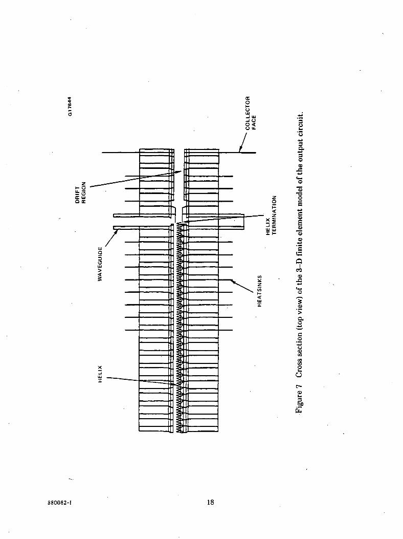
3u'«•fa>
|
OCO
Os-u
s
CO
<2•u
c—O
T'>
O'̂ 3o0)
oO
c-
a
880082-1 18
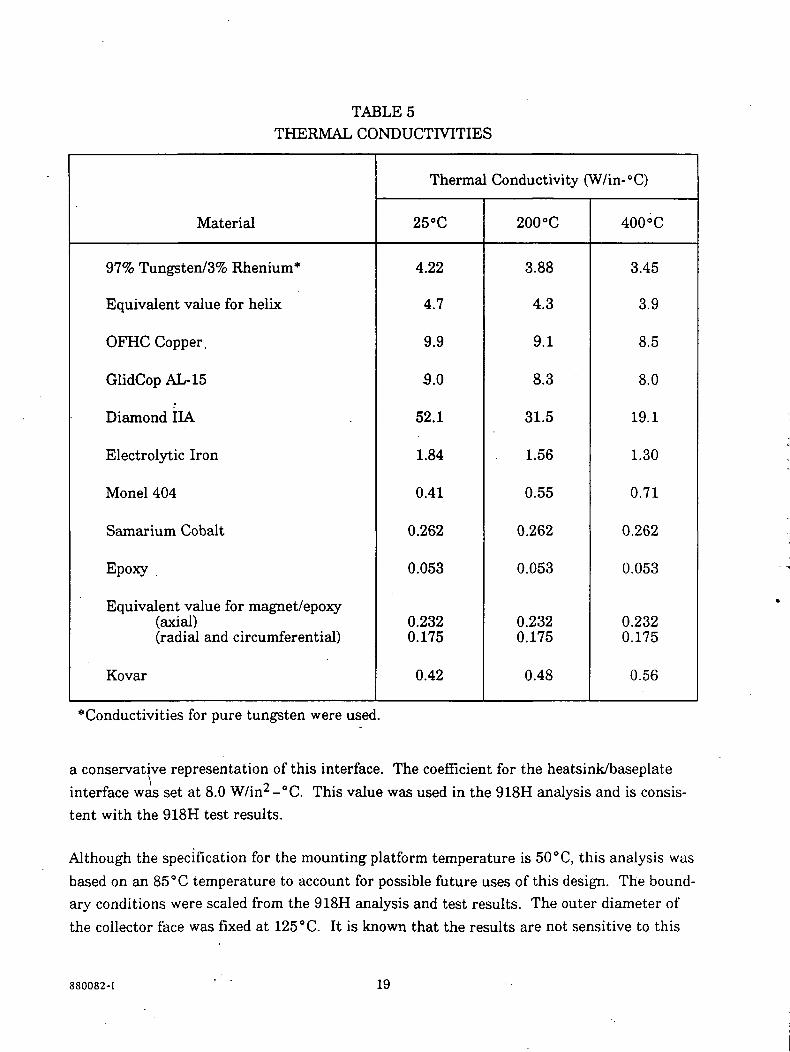
TABLESTHERMAL CONDUCTIVITIES
Material
97% Tungsten/3% Rhenium*
Equivalent value for helix
OFHC Copper.
GlidCop AL-15
Diamond IIA
Electrolytic Iron
Monel 404
Samarium Cobalt
Epoxy
Equivalent value for magnet/epoxy(axial)(radial and circumferential)
Kovar
Thermal Conductivity (W/in-°C)
25°C
4.22
4.7
9.9
9.0
52.1
1.84
0.41
0.262
0.053
0.2320.175
0.42
200°C
3.88
4.3
9.1
8.3
31.5
1.56
0.55
0.262
0.053
0.2320.175
0.48
400°C
3.45
3.9
8.5
8.0
19.1
1.30
0.71
0.262
0.053
0.2320.175
0.56
* Conductivities for pure tungsten were used.
a conservative representation of this interface. The coefficient for the heatsink/baseplate
interface was set at 8.0 W/in2-°C. This value was used in the 918H analysis and is consis-tent with the 918H test results.
Although the specification for the mounting platform temperature is 50 °C, this analysis was
based on an 85°C temperature to account for possible future uses of this design. The bound-ary conditions were scaled from the 918H analysis and test results. The outer diameter ofthe collector face was fixed at 125 °C. It is known that the results are not sensitive to this
880082-1 19
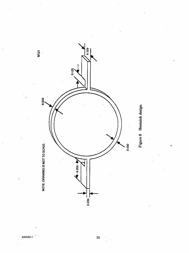
g,
8•o_c'33-*jee
00
2
880082-1 ' 20
assumption because preliminary runs showed that a 10 °C change in this value caused only a2°C change in the peak helix temperature. The baseplate temperature at the heatsink inter-
face was fixed at 100°C. The end of the model (gun side) was adiabatic.
The distribution of the power shown in Figure 9 indicates a total of 14.1 watts to be dissi-pated on the last inch of the helix. For this analysis, the distribution has been assumed tobe uniform over each quarter inch with the power applied directly to each node of the helix.The drift region was assumed to intercept 2.5 watts distributed uniformly over its length.The power was applied to the nodes at the inner diameter of the barrel between the wave-guide and the collector face. Finally, 2.5 watts were distributed uniformly over the area ofthe collector face up to a 0.75-inch diameter.
The results of the analysis of the copper sleeve case showed that the peak helix temperaturewas 194°C. This occurred just beyond the last helix/rod contact point at the end of the rods.The temperature distribution through the cross section at the end of the rods is shown inFigure 10. This illustrates the temperature drop from the helix to the inner diameter of thebarrel. There is a 30°C drop across the helix/rod interface and an 8°C drop across the rod/
sleeve interface. Due to the high thermal conductivity of diamond, there is only a 2°C dropbetween the inner and outer edges of the rod. The temperature drop between the inner andouter diameters of the copper sleeve is insignificant, but the drop at the sleeve/barrel inter-face is over 20 °C. This conflicts with the circuit thermal test results, which show that theactual drop across this interface is very small. It is believed that the presence of the goldplating on the outer diameter of the sleeve may be responsible for the formation of a bond atthis interface.* Therefore, the assumption used in the thermal analysis was overly conserva-tive. If a more realistic assumption had been used, the predicted sleeve temperature wouldhave been lower. This would have caused slightly higher helix/rod and rod/sleeve contactareas and pressures in the structural analysis and, consequently, lower temperature drops inthe thermal analysis.
Table 6 shows the axial temperature distribution in the circuit by giving the temperatures atfour cross sections. Structural runs for the operating condition were made using these foursets of temperatures. The resultant areas and pressures for the cross section at the end ofthe rods were reported in Section 2.3. The results for the other three cross sections werealso quite similar.
The results of the GlidCop sleeve case showed that the peak helix temperature was 192 °C.As in the copper sleeve case, this occurred just beyond the last helix/rod contact point. Thetemperature distribution through the cross section at the end of the rods is shown in Fig-ure 11. The axial temperature distribution is shown in Table 7. The predicted temperatures
880082-1 21
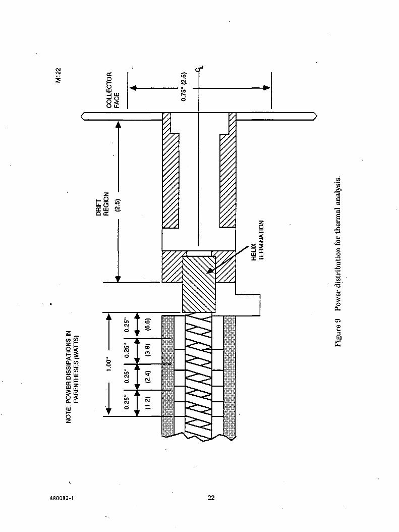
CNJCNJ
c03
"3
<u-U
i.-fcjW•3L.CD '
O
0,
C50)
I
880082-1 22
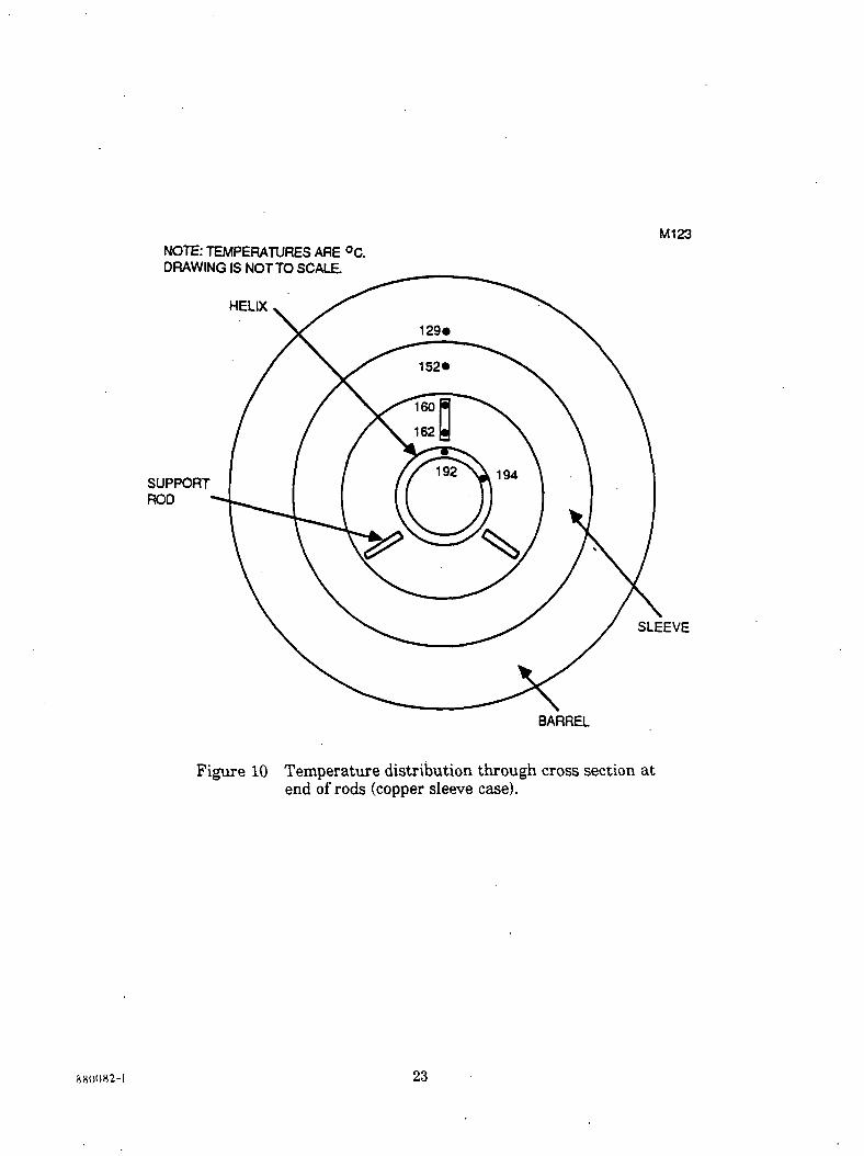
M123NOTE: TEMPERATURES ARE °C.DRAWING IS NOT TO SCALE
HELIX
SUPPORTROD
SLEEVE
BARREL
Figure 10 Temperature distribution through cross section atend of rods (copper sleeve case).
880082-1 23
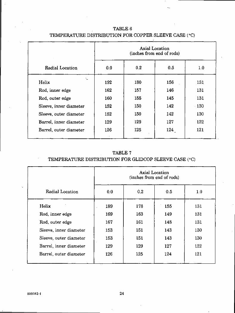
TABLE 6TEMPERATURE DISTRIBUTION FOR COPPER SLEEVE CASE (°C)
Radial Location
Helix
Rod, inner edge
Rod, outer edge
Sleeve, inner diameter
Sleeve, outer diameter
Barrel, inner diameter
Barrel, outer diameter
Axial Location(inches from end of rods)
0.0
192
162
160
152
152
129
126
0.2
180
157
155
150
150
129
125
0.5
156
146
145
142
142
127
124^
1.0
131
131
131
130
130
122
121
TABLE 7TEMPERATURE DISTRIBUTION FOR GLIDCOP SLEEVE CASE (°C)
Radial Location
Helix
Rod, inner edge
Rod, outer edge
Sleeve, inner diameter
Sleeve, outer diameter
Barrel, inner diameter
Barrel, outer diameter
Axial Location(inches from end of rods)
0.0
189
169
167
153
153
129
126
0.2
178
163
161
151
151
129
125
0.5
155
149
148
143
143
127
124
1.0
131
131
131
130
130
122
121
880082-1 24
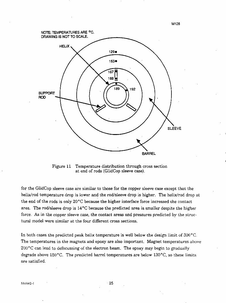
M126
NOT!: TEMPERATURES ARE °C.DRAWING IS NOT TO SCALE
HELIX
SUPPORTROD
SLEEVE
BARREL
Figure 11 Temperature distribution through cross sectionat end of rods (GlidCop sleeve case).
for the GlidCop sleeve case are similar to those for the copper sleeve case except that thehelix/rod temperature drop is lower and the rod/sleeve drop is higher. The helix/rod drop atthe end of the rods is only 20 °C because the higher interface force increased the contact
area. The rod/sleeve drop is 14°C because the predicted area is smaller despite the higherforce. As in the copper sleeve case, the contact areas and pressures predicted by the struc-tural model were similar at the four different cross sections.
In both cases the predicted peak helix temperature is well below the design limit of 300° C.The temperatures in the magnets and epoxy are also important. Magnet temperatures above200°C can lead to defocussing of the electron beam. The epoxy may begin to gradually
degrade above 150°C. The predicted barrel temperatures are below 130°C, so these limitsare satisfied.
880082-1 25
4.0 LONG-TERM OPERATION
The 953H TWT must be able to perform for a long period of time without a degradation in
performance. If the helix temperature were to rise above 300°C during operation, the prob-ability of an observable change in electrical performance would increase rapidly. Such atemperature rise could be attributable to creep strain in the output circuit. Therefore, anestimate was made of the effect of creep on the thermal performance of the circuit after100,000 hours (11.4 years) of operation. This was assumed to be the end-of-life condition.Both the copper sleeve and GlidCop sleeve cases were considered.
Creep is a continuous increase in deformation (strain) with time under a constant load(stress). Material creep rates are highly dependent upon temperature. Relaxation is arelated phenomenon in which the load continuously decreases with time under a constantdeformation. In many applications, both phenomena occur simultaneously and are referredto as "creep". In the output circuit, the compressive forces that hold the componentstogether will gradually decrease during operation. Local deformation may also cause thecontact areas at the critical interfaces to change.
A structural analysis for the long-term operating condition of a copper-sleeved circuit wasperformed. This analysis continued from the results of a preliminary analysis of the initialoperating condition. The initial operating temperatures had been estimated as follows:
helix, 180°C; rods, 130°C; sleeve, 120°C; barrel, 115°C. The applied temperatures remainedconstant throughout the analysis. Creep strain was allowed only in the copper sleeve andhelix coating because the creep rates in the other materials would be insignificant at thesetemperatures.
Primary creep refers to the strain that occurs soon after the application of a load. Since theprimary creep rate decreases rapidly, it is of most importance for short-term effects. Follow-ing primary creep, the secondary creep rate is essentially constant over a long period of time.Therefore, the secondary creep rate of copper was used in the analysis for the long-termoperating condition. The secondary creep rates of copper and GlidCop are given in Table 8.The data from Jenkins and Digges4 and Davis^ are from uniaxial tension .creep tests. Thevalues for GlidCop were derived from uniaxial tension relaxation tests presented by SCM.^
In the finite element analysis, the multidimensional creep effects were extrapolated from the
uniaxial test data in the same way as the plasticity effects. The test data near 120 °C wasused to develop the equation governing the creep strain in the copper sleeve:
e = (4.0 x 10⁻¹⁶) exp (-6000/T) a4
880082-1 27
PRECEDING PAGE BLANK NOT FILMED
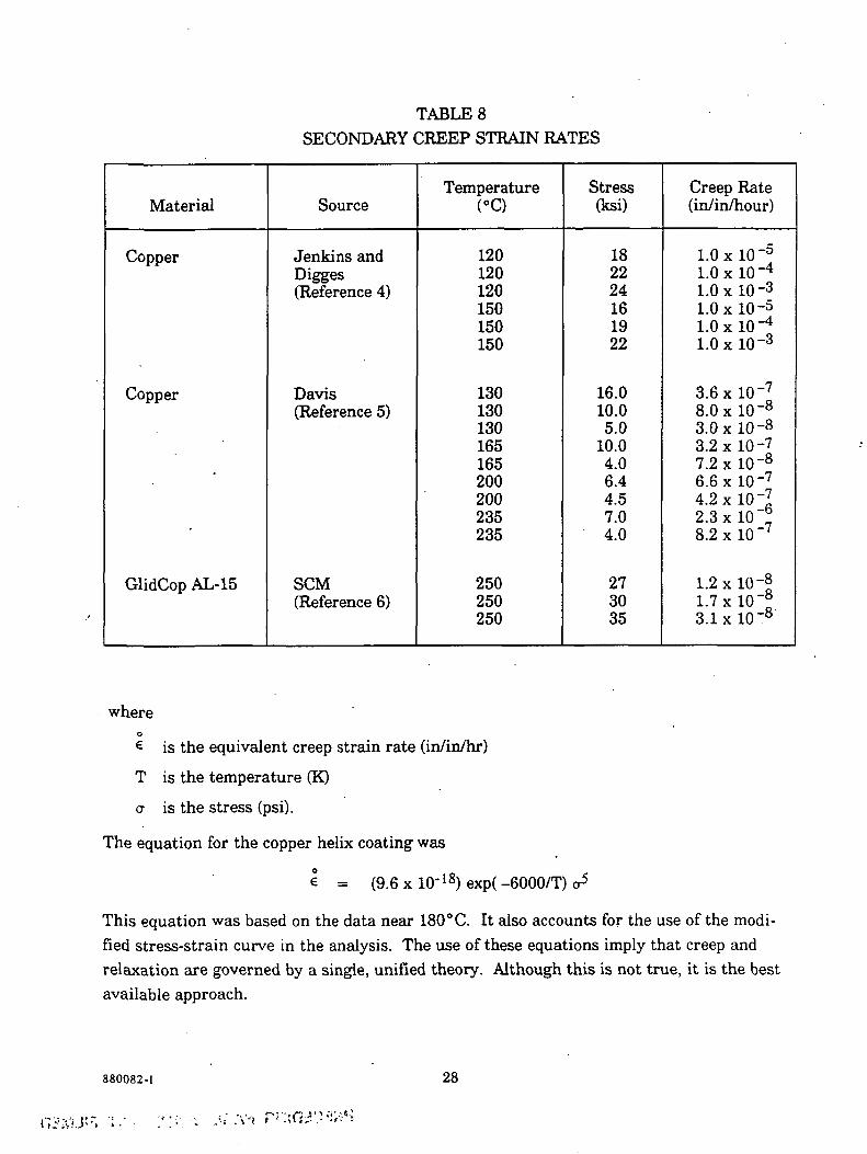
TABLESSECONDARY CREEP STRAIN RATES
Material
Copper
Copper
.
GlidCop AL-15
Source
Jenkins andDigges(Reference 4)
Davis(Reference 5)
SCM(Reference 6)
Temperature(°C)
120120120150150150
130130130165165200200235235
250250250
Stress(ksi)
182224161922
16.010.05.0
10.04.06.44.57.04.0
273035
Creep Rate(in/in/hour)
l.OxlO'51.0 xlO"4
l .OxlO-3
1.0 x 10⁻⁵l .OxlO-4
1.0 x 10 ~3
3.6xlO-7
3.0x10-83.2x10-77.2xlO-8
6.6 x 10 -7
4.2xlO-J,2.3x10'!?8.2xlO"7
1.2xlO-f1.7 x 10 ~8
3.1X10'8
whereo6 is the equivalent creep strain rate (in/in/hr)
T is the temperature (K)
a is the stress (psi).
The equation for the copper helix coating' was
e = (9.6xlO-18)exp(-6000/T)o5
This equation was based on the data near 180°C. It also accounts for the use of the modi-fied stress-strain curve in the analysis. The use of these equations imply that creep andrelaxation are governed by a single, unified theory. Although this is not true, it is the bestavailable approach.
880082-1 28
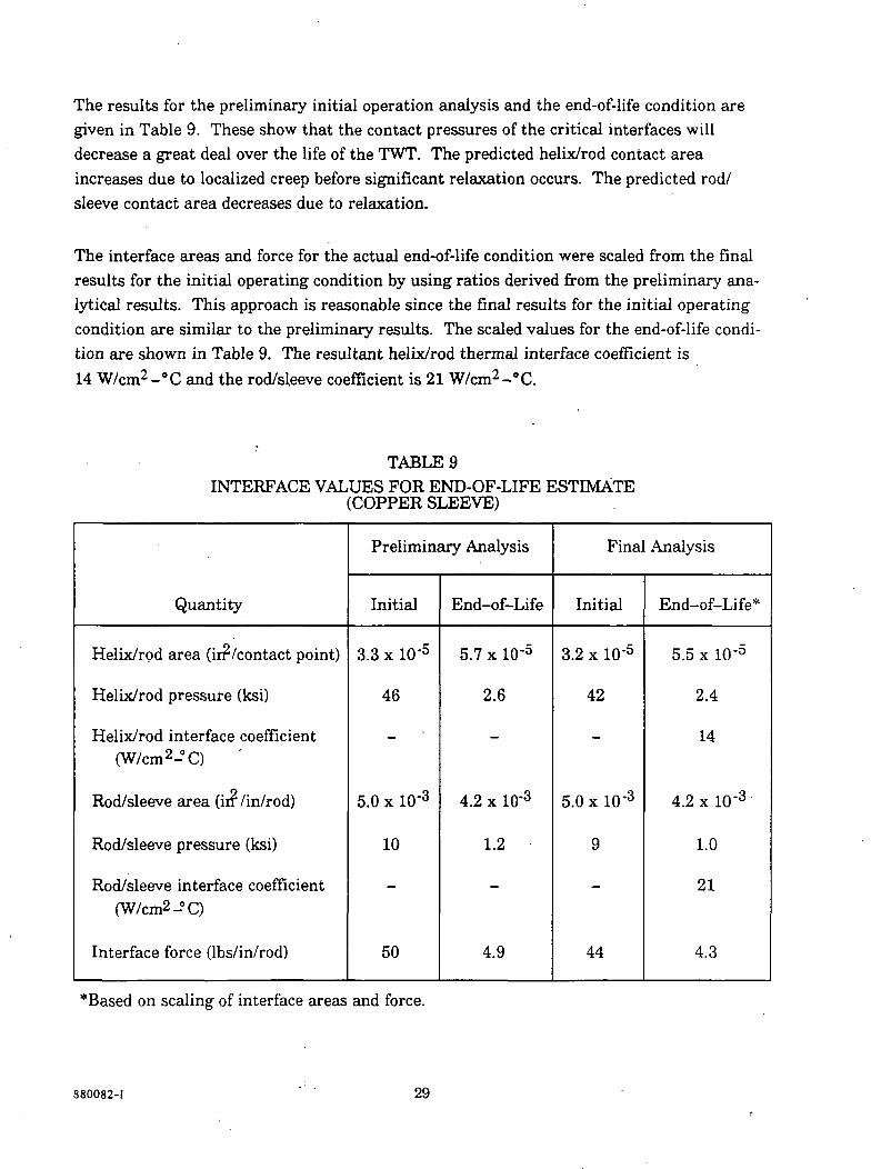
The results for the preliminary initial operation analysis and the end-of-life condition aregiven in Table 9. These show that the contact pressures of the critical interfaces willdecrease a great deal over the life of the TWT. The predicted helix/rod contact areaincreases due to localized creep before significant relaxation occurs. The predicted rod/sleeve contact area decreases due to relaxation.
The interface areas and force for the actual end-of-life condition were scaled from the finalresults for the initial operating condition by using ratios derived from the preliminary ana-lytical results. This approach is reasonable since the final results for the initial operatingcondition are similar to the preliminary results. The scaled values for the end-of-life condi-tion are shown in Table 9. The resultant helix/rod thermal interface coefficient is14 W/cm2-°C and the rod/sleeve coefficient is 21 W/cm2-°C.
TABLE 9INTERFACE VALUES FOR END-OF-LIFE ESTIMATE
(COPPER SLEEVE)
Quantity
Helix/rod area (ir? /contact point)
Helix/rod pressure (ksi)
Helix/rod interface coefficient(W/cm2-C)
Rod/sleeve area (in /in/rod)
Rod/sleeve pressure (ksi)
Rod/sleeve interface coefficient(W/cm2-°C)
Interface force (Ibs/in/rod)
Preliminary Analysis
Initial
3.3 x 10'5
46
-
5.0 x 10'3
10
-
50
End-of-Life
5.7 x 10'5
2.6
-
4.2 x 10'3
1.2
-
4.9
Final Analysis
Initial
3.2 x 10'5
42
-
5.0 xlO'3
9
-
44
End-of-Life*
5.5 x 10'5
2.4
14
4.2 x 10'3
1.0
21
4.3
"Based on scaling of interface areas and force.
880082-1 29
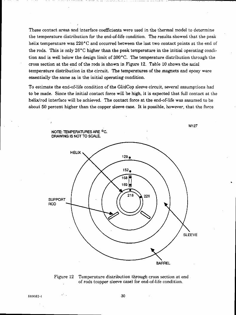
These contact areas and interface coefficients were used in the thermal model to determinethe temperature distribution for the end-of-life condition. The results showed that the peakhelix temperature was 220°C and occurred between the last two contact points at the end of
the rods. This is only 26 °C higher than the peak temperature in the initial operating condi-
tion and is well below the design limit of 300 °C. The temperature distribution through thecross section at the end of the rods is shown in Figure 12. Table 10 shows the axialtemperature distribution in the circuit. The temperatures of the magnets and epoxy wereessentially the same as in the initial operating condition.
To estimate the end-of-life condition of the GlidCop sleeve circuit, several assumptions hadto be made. Since the initial contact force will be high, it is expected that full contact at thehelix/rod interface will be achieved. The contact force at the end-of-life was assumed to beabout 50 percent higher than the copper sleeve case. It is possible, however, that the force
M127
NOTE: TEMPERATURES ARE °C.DRAWING IS NOT TO SCALE
HELIX
SUPPORTROD
SLEEVE
BARREL
Figure 12 Temperature distribution through cross section at endof rods (copper sleeve case) for end-of-life condition.
880082-1 30
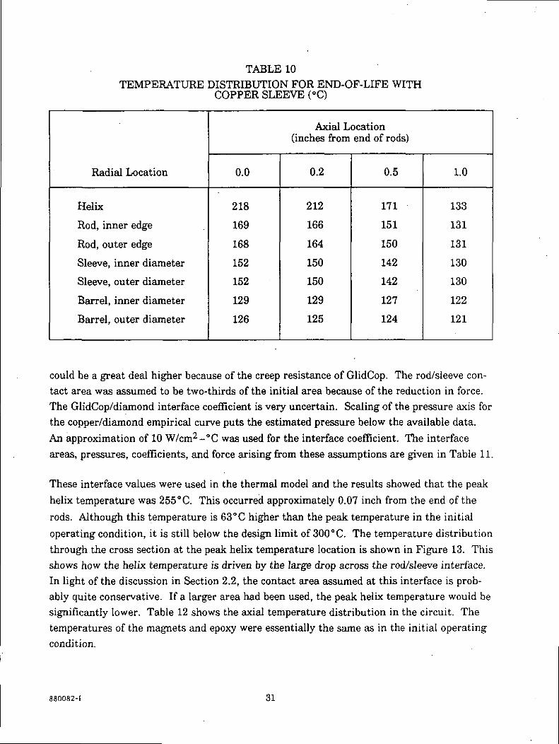
TABLE 10TEMPERATURE DISTRIBUTION FOR END-OF-LIFE WITH
COPPER SLEEVE (°C)
Radial Location
Helix
Rod, inner edge
Rod, outer edge
Sleeve, inner diameter
Sleeve, outer diameter
Barrel, inner diameter
Barrel, outer diameter
Axial Location(inches from end of rods)
0.0
218
169
168
152
152
129
126
0.2
212
166
164
150
150
129
125
0.5
171
151
150
142
142
127
124
1.0
133
131
131
130
130
122
121
could be a great deal higher because of the creep resistance of GlidCop. The rod/sleeve con-tact area was assumed to be two-thirds of the initial area because of the reduction in force.The GlidCop/diamond interface coefficient is very uncertain. Scaling of the pressure axis forthe copper/diamond empirical curve puts the estimated pressure below the available data.An approximation of 10 W/cm^-°C was used for the interface coefficient. The interfaceareas, pressures, coefficients, and force arising from these assumptions are given in Table 11.
These interface values were used in the thermal model and the results showed that the peakhelix temperature was 255°C. This occurred approximately 0.07 inch from the end of the
rods. Although this temperature is 63°C higher than the peak temperature in the initial
operating condition, it is still below the design limit of 300°C. The temperature distributionthrough the cross section at the peak helix temperature location is shown in Figure 13. Thisshows how the helix temperature is driven by the large drop across the rod/sleeve interface.In light of the discussion in Section 2.2, the contact area assumed at this interface is prob-ably quite conservative. If a larger area had been used, the peak helix temperature would besignificantly lower. Table 12 shows the axial temperature distribution in the circuit. Thetemperatures of the magnets and epoxy were essentially the same as in the initial operatingcondition.
880082-1 31
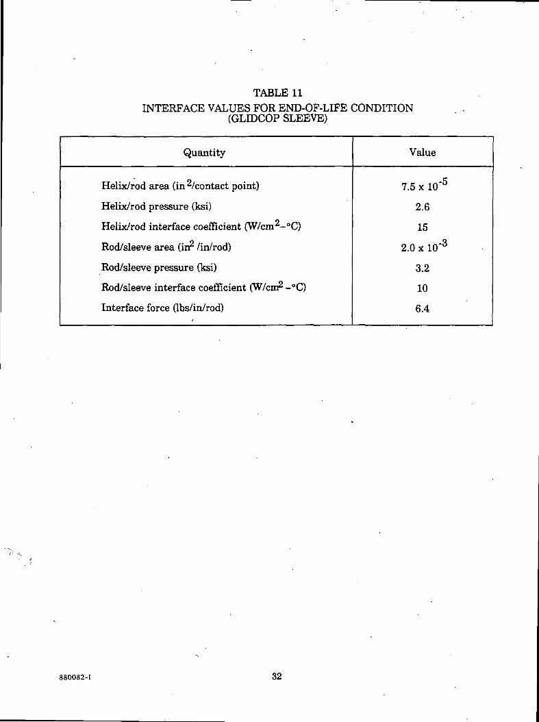
TABLE 11INTERFACE VALUES FOR END-OF-LIFE CONDITION
(GLIDCOP SLEEVE)
Quantity Value
Helix/rod area (in 2/contact point)
Helix/rod pressure (ksi)
Helix/rod interface coefficient (W/cm2-°C)
Rod/sleeve area (in2 /in/rod)
Rod/sleeve pressure (ksi)
Rod/sleeve interface coefficient (W/cm2 -°C)
Interface force (Ibs/in/rod)
7.5 x 10
2.6
15
2.0 x 10
3.2
10
6.4
-5
-3
880082-1 32
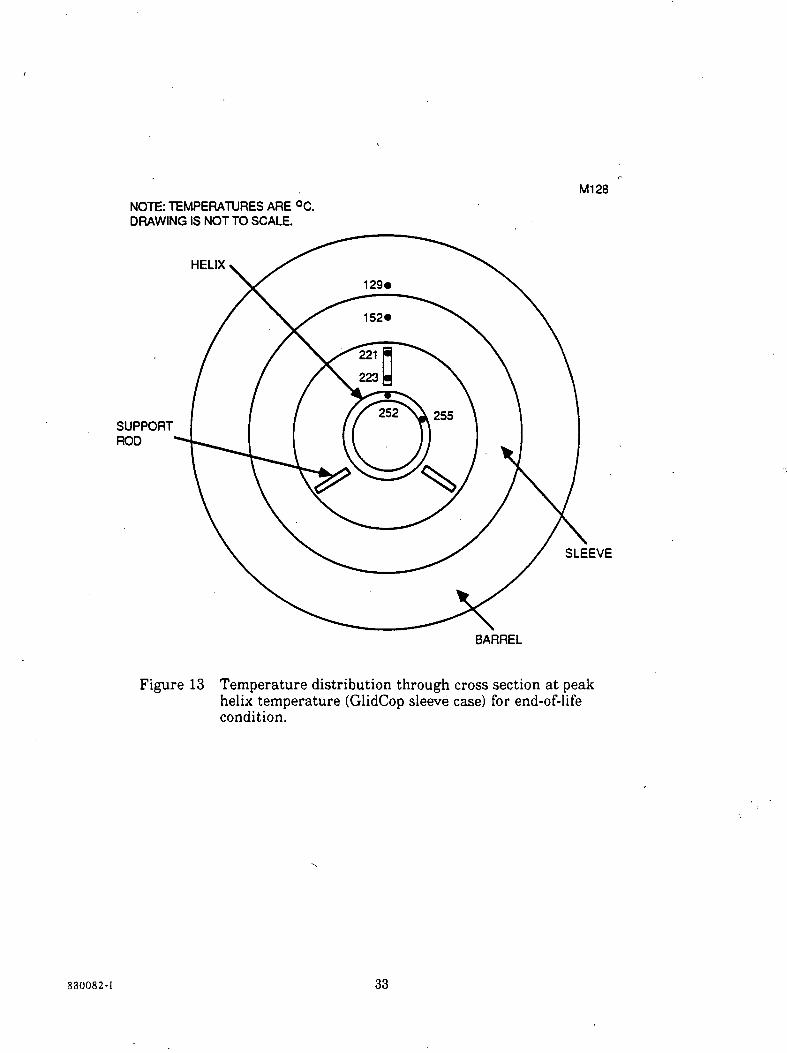
M128
NOTE: TEMPERATURES ARE °C.DRAWING IS NOT TO SCALE.
HELIX
SUPPORTROD
SLEEVE
BARREL
Figure 13 Temperature distribution through cross section at peakhelix temperature (GlidCop sleeve case) for end-of-lifecondition.
880082-1 33
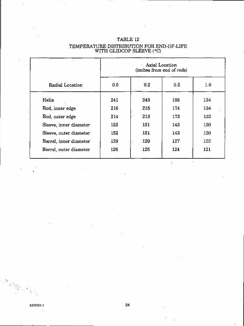
TABLE 12TEMPERATURE DISTRIBUTION FOR END-OF-LIFE
WITH GLIDCOP SLEEVE (°C)
Radial Location
Helix
Rod, inner edge
Rod, outer edge
Sleeve, inner diameter
Sleeve, outer diameter
Barrel, inner diameter
Barrel, outer diameter
Axial Location(inches from end of rods)
0.0
241
216
214
152
152
129
126
0.2
243
215
213
151
151
129
125
0.5
188
174
173
143
143
127
124
1.0
134
134
133
130
130
122
121
880082-1 34
5.0 CONCLUSION
The combined structural and thermal analysis of the 953H output circuit has shown that itwill be able to handle the required thermal loads. The predicted peak helix temperaturesduring the initial operating condition were 194 °C for the copper sleeve design and 192 °C forthe GlidCop sleeve design. The estimates for the long-term operating condition predictedpeaks of 220 °C for the copper sleeve and 255 °C for the GlidCop sleeve. Since these tempera-
tures are below the design limit of 300° C, both configurations are considered to besatisfactory.
It should be noted that the purpose of the analysis was to judge both configurations by thedesign limit rather than providing a comparison between designs. Conservative assumptionswere made throughout this analysis because the final results were to be compared to anabsolute limit. The analytical approaches used in the bakeout analysis and the long-termoperation estimates were much more conservative for the GlidCop sleeve design than thecopper sleeve design. Due to this inequity, a direct comparison between the two sets ofresults could lead to misleading conclusions. It is likely that the actual temperatures for theGlidCop design will be considerably lower than predicted. In fact, it is possible that the tem-peratures could be lower than those for the copper sleeve design.
To improve the understanding of the GlidCop design, experiments should be conducted todetermine the GlidCop/diamond thermal interface coefficient as a function of pressure.Extending the existing curves for the other interfaces into the low and high pressure regionswould also be useful in future analyses. In addition, better definition of the other GlidCopproperties would be helpful.
880082-1 35
6.0 REFERENCES
1. P.C. Kohnke, ANSYS Theoretical Manual, Swanson Analysis Systems, Inc.,March 1, 1986.
2. 0. Sauseng, "Heat Transfer Data for Helix Circuit Materials," Hughes EDDReport, p. 19, August 1984.
3. Ibid., p. 23.
4. W.D. Jenkins and T.G. Digges, "Creep of Annealed and Cold-Drawn High PurityCopper," J. Research National Bureau of Standards, Vol. 47, 1951, p. 272-287.
5. E.A. Davis, "Creep and Relaxation of Oxygen-Free Copper," Trans. Am. Soc.Mech. Engrs. 65, [A] 101 (1943).
6. SCM Metal Products, Vendor-supplied data, 1985.
880082-1 37PRECEDING PAGE BLANK NOT FILMED
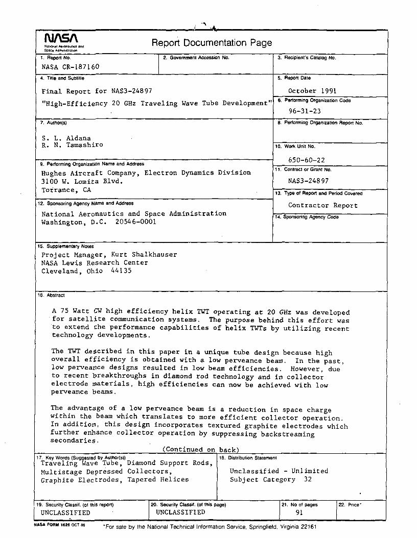
NASANational Aeronautics andSpace Administration
Report Documentation Page1. Report No.
NASA CR-1871602. Government Accession No. 3. Recipient's Catalog No.
4. Title and Subtitle
Final Report for NAS3-24897
"High-Efficiency 20 GHz Traveling Wave Tube Development"
5. Report Date
October 19916. Performing Organization Code
96-31-23
7. Author(s)
S. L. AldanaR. N. Tamashiro
6. Performing Organization Report No.
9. Performing Organization Name and Address
Hughes Aircraft Company, Electron Dynamics Division3100 W. Lomita Blvd.Torrance, CA
10. Work Unit No.
650-60-2211. Contract or Grant No.
NAS3-24897
12. Sponsoring Agency Name and Address
National Aeronautics and Space AdministrationWashington, D.C. 20546-0001
13. Type of Report and Period Covered
Contractor Report
14. Sponsoring Agency Code
15. Supplementary Notes
Project Manager, Kurt ShalkhauserNASA Lewis Research CenterCleveland, Ohio 44135
16. Abstract
A 75 Watt CW high efficiency helix TWT operating at 20 GHz was developedfor satellite communication systems. The purpose behind this effort wasto extend the performance capabilities of helix TWTs by utilizing recenttechnology developments.
The TWT described in this paper in a. unique tube design because highoverall efficiency is obtained with a low perveance beam. In the past,low perveance designs resulted in low beam efficiencies. However, due'to recent breakthroughs in diamond rod technology and in collectorelectrode materials, high efficiencies can now be achieved with lowperveance beams.
The advantage of a low perveance beam is a reduction in space chargewithin the beam which translates to more efficient collector operation.In addition, this design incorporates textured graphite electrodes whichfurther enhance collector operation by suppressing backstreamingsecondaries.
(Continued on back)17. Key Words (Suggested by Author(s))
Traveling Wave Tube, Diamond Support Rods,Multistage Depressed Collectors,Graphite Electrodes, Tapered Helices
19. Security Classif. (of this report)
UNCLASSIFIED
18. Distribution Statement
Unclassified - UnlimitedSubject Category 32
20. Security Classif. (of this page)
UNCLASSIFIED
21. No of pages 22. Price*
91
NASA FORM 1626 OCT 86 'For sale by the National Technical Information Service, Springfield, Virginia 22161

.16. Abstract (Continued) fJ
The diamond supported helix circuit features low rf losses, highinteraction impedance, good thermal handling capability and has beendesigned to compensate for the low perveance beam. The circuitincorporates five mil (0.005 in.) wide diamonds as the helix support rodmaterial. A non-bonded non-brazed diamond rod fabrication technique haseliminated the losses previously encountered with brazed diamond/helixinterfaces without sacrificing thermal handling requirements. In thisapplication, the circuit cold loss is measured to be 0.3 dB/in at 20GHz. In comparison, the cold loss for an identical circuitincorporating 0.020 in. wide BeO rods is 1.5 dB/in.
One more feature of the tube design that will be discussed is theutilization of a velocity taper in the output helix that achieves lowsignal distortion while maintaining high efficiency.
Three breadboard units were fabricated under this program. One unitdemonstrated 100 watts RF output power, with excellent repeatability andno sign of degradation. The same TWT achieved 16.9 percent basic and54.6 percent overall efficiency setting a new bench mark in TWTtechnology for K-band devices. In contrast, 12 percent basic and48 percent overall was the best K-band TWT efficiency achieved in thepast.
The structural, thermal and electrical properties of diamonds arebecoming increasingly attractive with higher TWT operating frequencies.The techniques used to fabricate the present circuit are compatible withTWT electrical design requirements up to 60 GHz.


![DESIGN OF A HIGH POWER, HIGH EFFICIENCY KA- BAND HELIX TRAVELING-WAVE TUBE … · 2018. 1. 10. · applications [1{3]. The helix traveling-wave tube (TWT) is one of the most important](https://img.pdfslide.net/doc/110x75/60c51556e8f4c817594da965/design-of-a-high-power-high-efficiency-ka-band-helix-traveling-wave-tube-2018.jpg)