Embed Size (px)
Citation preview
High Frequency Devices and
Circuits
Jae-Sung Rieh
School of Electrical Engineering
Korea University
1
Outline
• High Frequency Applications
• High Frequency Semiconductor Devices
• High Frequency Semiconductor Circuits
2
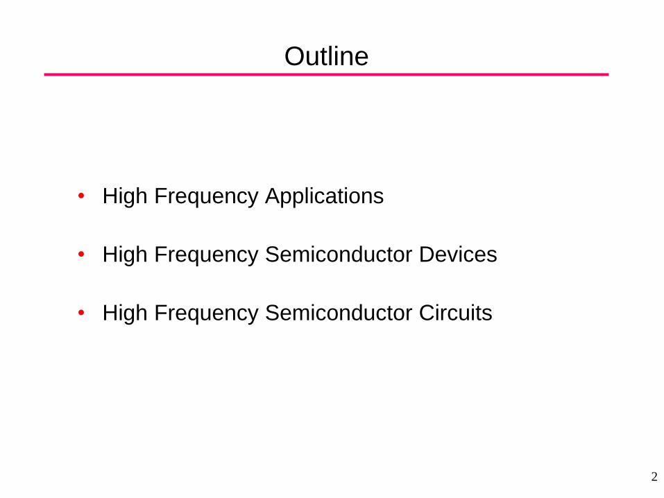
Various Application of RF and mm-wave
Wireline
Wireless
0.1 1 10 100 Freq [GHz]
Automotive radar (77GHz)
WPAN (60GHz)
LMDS (26GHz)
802.11a (5.8GHz)
802.11b/g/n (2.4GHz)
Cellular (~2GHz)
GPS (1.6GHz)
OC-192 (10Gbps)
0.1 1 10 100 Bit rate [Gbps]
OC-768 (40Gbps) OC-48 (2.5Gbps)
Imaging (94GHz)
3
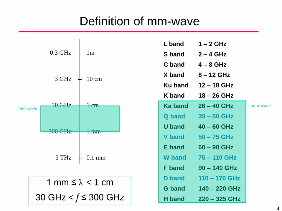
Definition of mm-wave
1m
10 cm
1 cm
1 mm
0.1 mm
0.3 GHz
3 GHz
30 GHz
300 GHz
3 THz
L band 1 – 2 GHz
S band 2 – 4 GHz
C band 4 – 8 GHz
X band 8 – 12 GHz
Ku band 12 – 18 GHz
K band 18 – 26 GHz
Ka band 26 – 40 GHz
Q band 30 – 50 GHz
U band 40 – 60 GHz
V band 50 – 75 GHz
E band 60 – 90 GHz
W band 75 – 110 GHz
F band 90 – 140 GHz
D band 110 – 170 GHz
G band 140 – 220 GHz
H band 220 – 325 GHz
mm-wave mm-wave
1 mm ≤ l < 1 cm
30 GHz < f ≤ 300 GHz
4
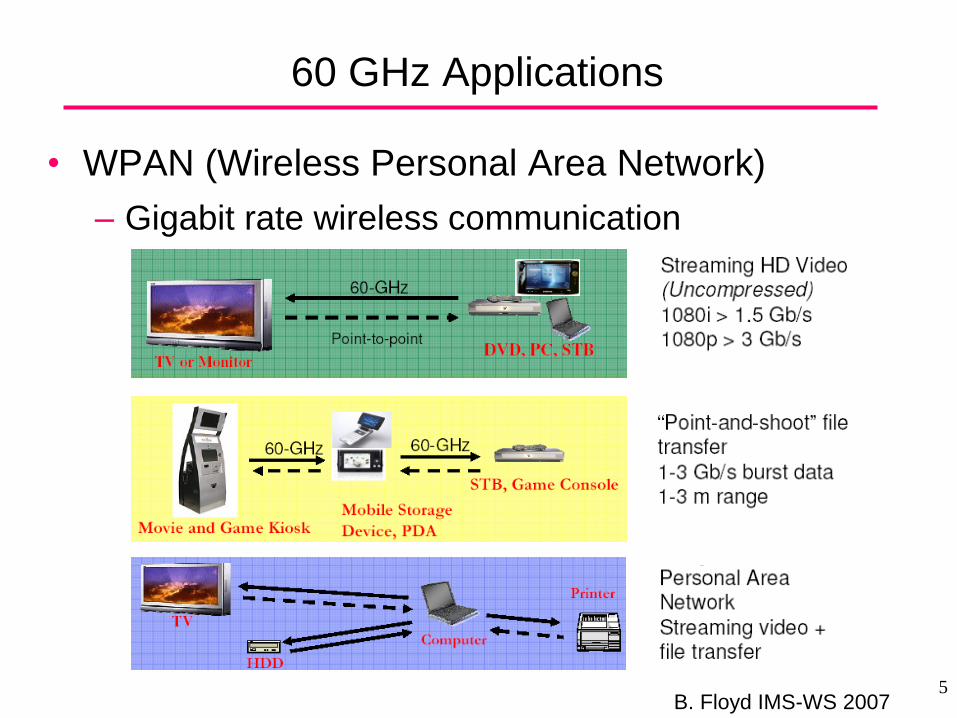
60 GHz Applications
• WPAN (Wireless Personal Area Network)
– Gigabit rate wireless communication
B. Floyd IMS-WS 2007 5
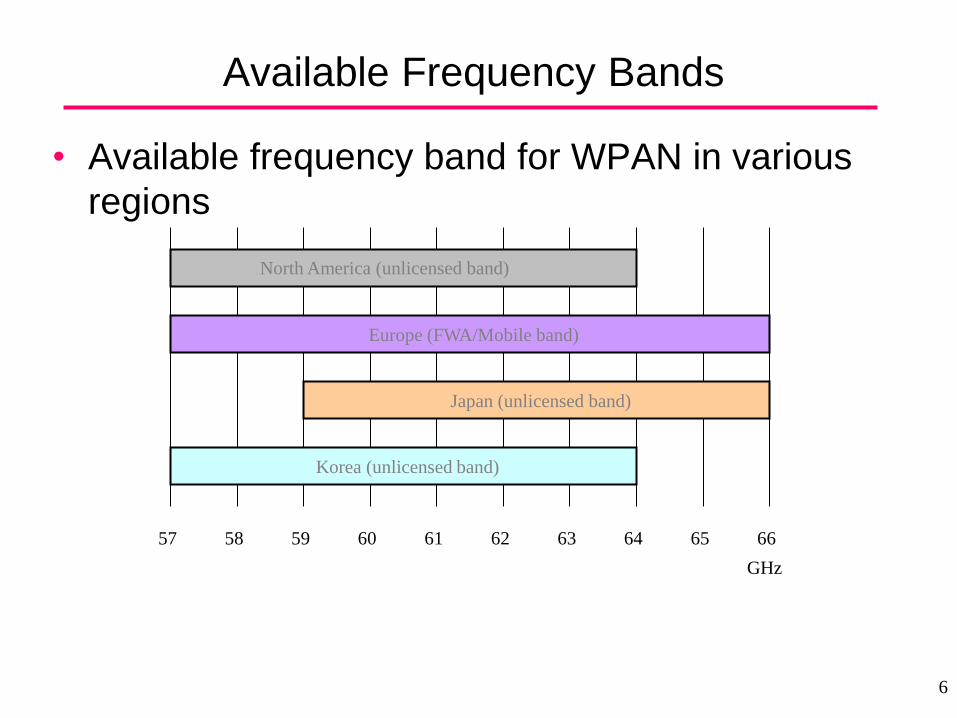
Available Frequency Bands
• Available frequency band for WPAN in various
regions
GHz
North America (unlicensed band)
Europe (FWA/Mobile band)
Japan (unlicensed band)
Korea (unlicensed band)
57 58 59 60 61 62 63 64 65 66
6
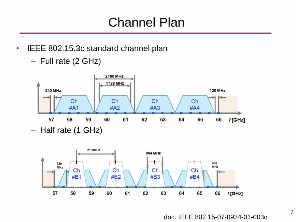
Channel Plan
• IEEE 802.15.3c standard channel plan
– Full rate (2 GHz)
– Half rate (1 GHz)
doc. IEEE 802.15-07-0934-01-003c 7
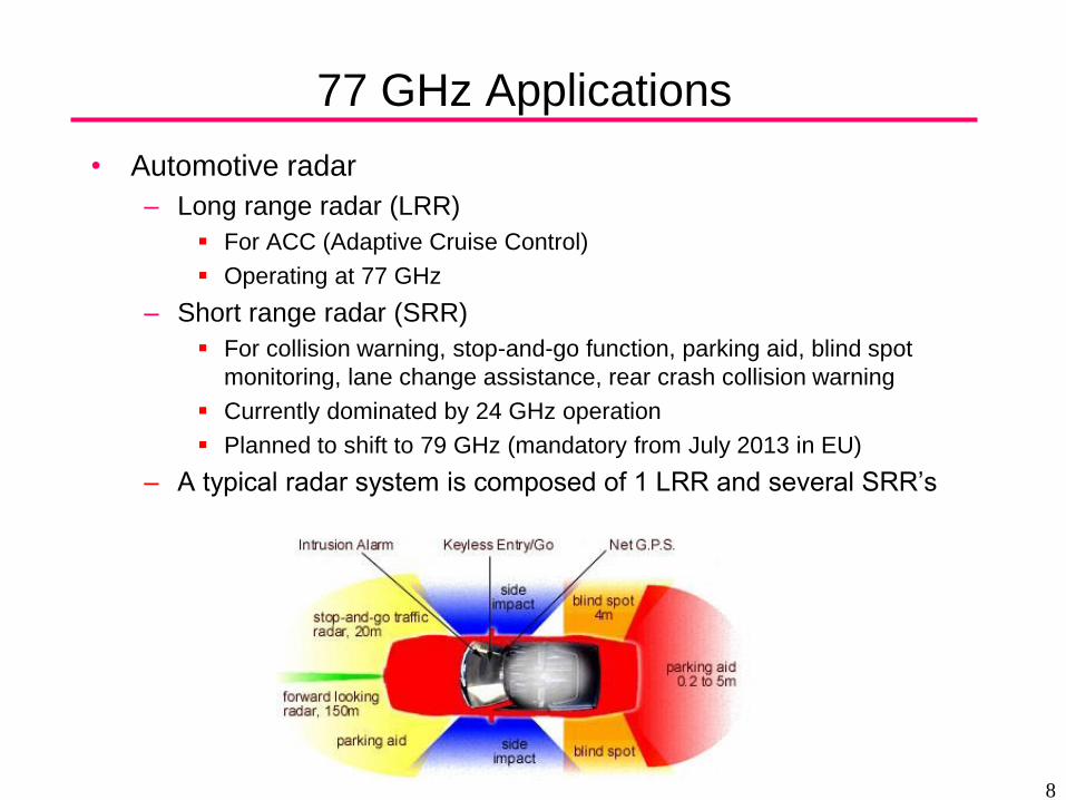
77 GHz Applications
• Automotive radar
– Long range radar (LRR)
For ACC (Adaptive Cruise Control)
Operating at 77 GHz
– Short range radar (SRR)
For collision warning, stop-and-go function, parking aid, blind spot
monitoring, lane change assistance, rear crash collision warning
Currently dominated by 24 GHz operation
Planned to shift to 79 GHz (mandatory from July 2013 in EU)
– A typical radar system is composed of 1 LRR and several SRR’s
8
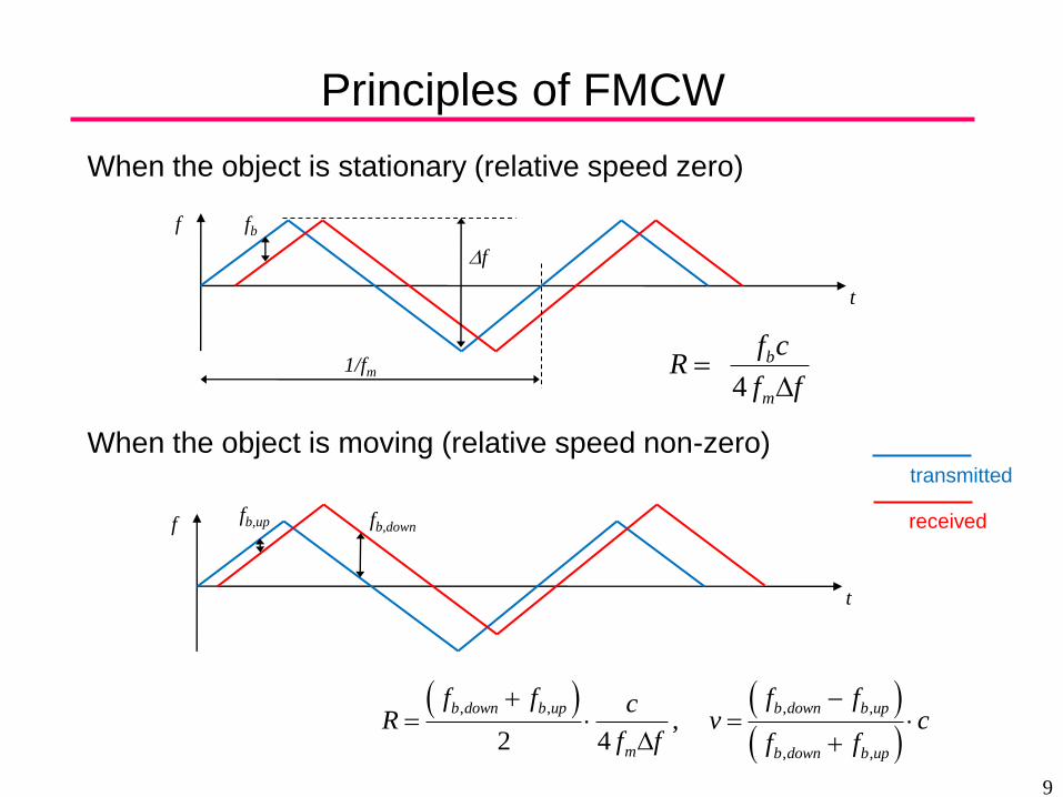
Principles of FMCW
When the object is stationary (relative speed zero)
When the object is moving (relative speed non-zero)
t
f fb
Df
1/fm 4
b
m
f cR
f f
D
t
f fb,up fb,down
, , , ,
, ,
, 2 4
b down b up b down b up
m b down b up
f f f fcR v c
f f f f
D
transmitted
received
9
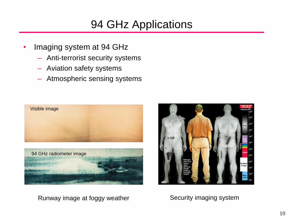
94 GHz Applications
• Imaging system at 94 GHz
– Anti-terrorist security systems
– Aviation safety systems
– Atmospheric sensing systems
Runway image at foggy weather Security imaging system
Visible image
94 GHz radiometer image
10
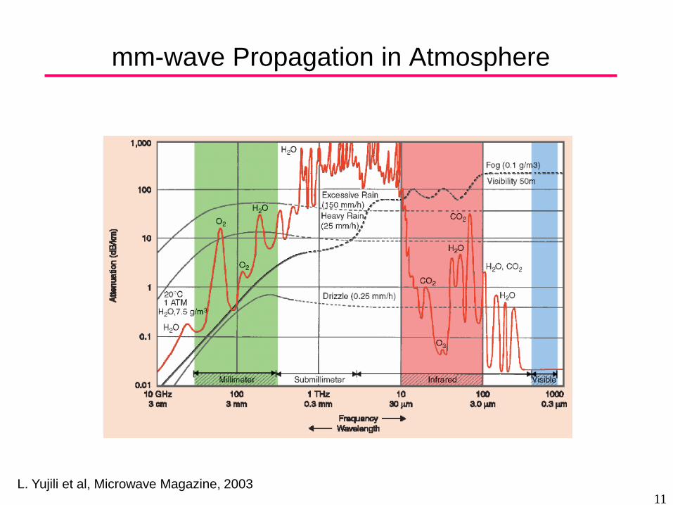
mm-wave Propagation in Atmosphere
11 L. Yujili et al, Microwave Magazine, 2003
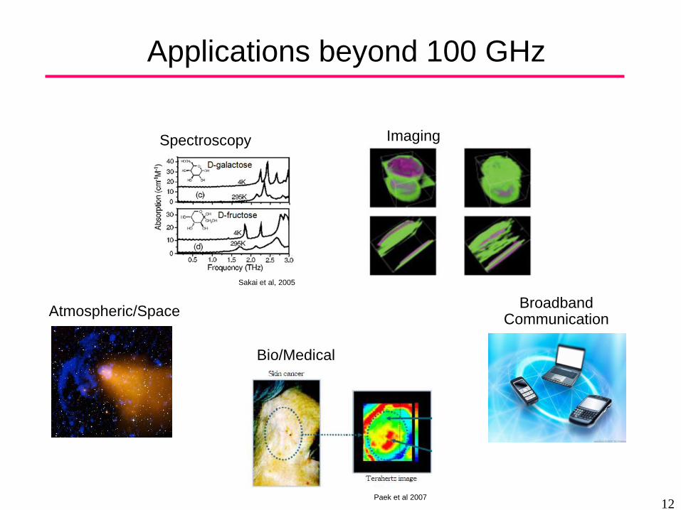
Applications beyond 100 GHz
Paek et al 2007
Bio/Medical
Atmospheric/Space Broadband
Communication
Spectroscopy
Sakai et al, 2005
Imaging
12
Outline
• High Frequency Applications
• High Frequency Semiconductor Devices
• High Frequency Semiconductor Circuits
13
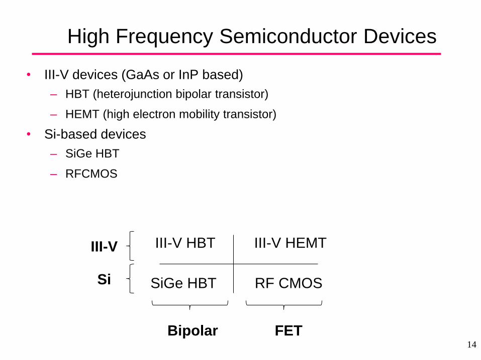
High Frequency Semiconductor Devices
• III-V devices (GaAs or InP based)
– HBT (heterojunction bipolar transistor)
– HEMT (high electron mobility transistor)
• Si-based devices
– SiGe HBT
– RFCMOS
III-V HBT III-V HEMT
SiGe HBT RF CMOS
III-V
Si
Bipolar FET 14
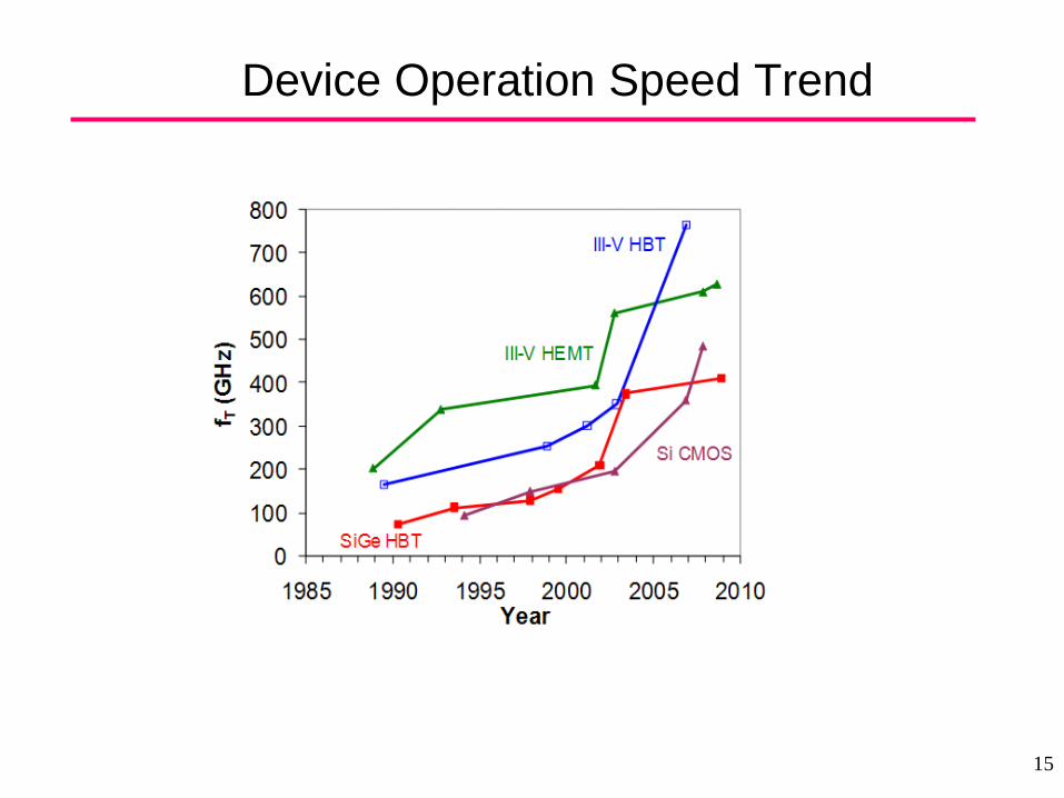
Device Operation Speed Trend
15
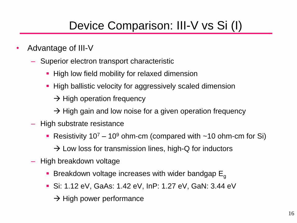
Device Comparison: III-V vs Si (I)
• Advantage of III-V
– Superior electron transport characteristic
High low field mobility for relaxed dimension
High ballistic velocity for aggressively scaled dimension
High operation frequency
High gain and low noise for a given operation frequency
– High substrate resistance
Resistivity 107 – 109 ohm-cm (compared with ~10 ohm-cm for Si)
Low loss for transmission lines, high-Q for inductors
– High breakdown voltage
Breakdown voltage increases with wider bandgap Eg
Si: 1.12 eV, GaAs: 1.42 eV, InP: 1.27 eV, GaN: 3.44 eV
High power performance
16
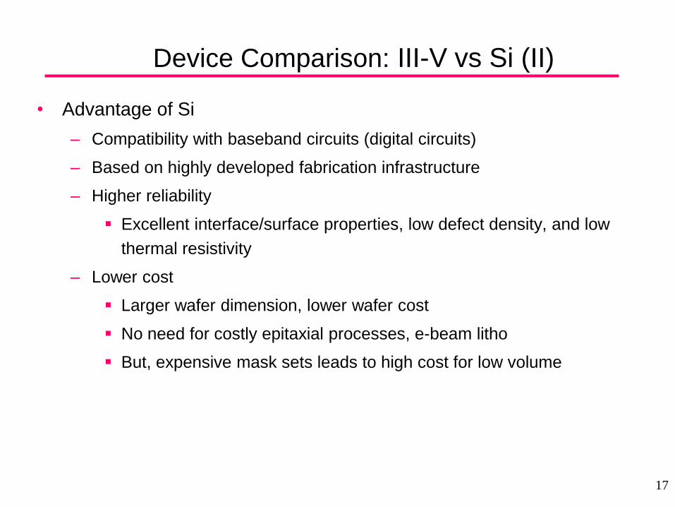
Device Comparison: III-V vs Si (II)
• Advantage of Si
– Compatibility with baseband circuits (digital circuits)
– Based on highly developed fabrication infrastructure
– Higher reliability
Excellent interface/surface properties, low defect density, and low
thermal resistivity
– Lower cost
Larger wafer dimension, lower wafer cost
No need for costly epitaxial processes, e-beam litho
But, expensive mask sets leads to high cost for low volume
17
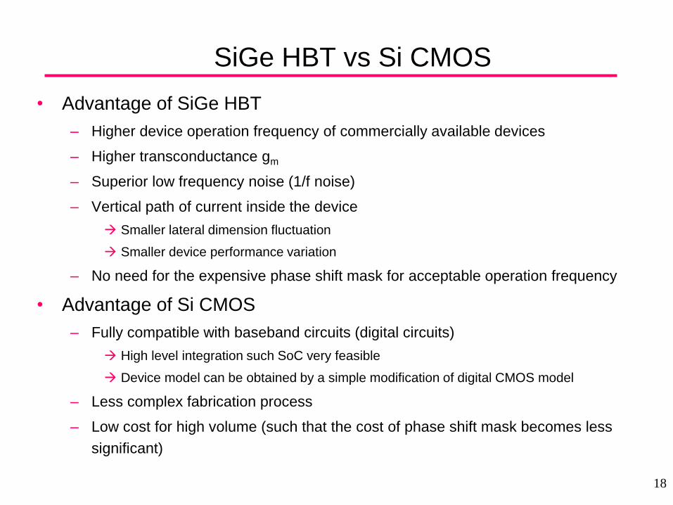
SiGe HBT vs Si CMOS
• Advantage of SiGe HBT
– Higher device operation frequency of commercially available devices
– Higher transconductance gm
– Superior low frequency noise (1/f noise)
– Vertical path of current inside the device
Smaller lateral dimension fluctuation
Smaller device performance variation
– No need for the expensive phase shift mask for acceptable operation frequency
• Advantage of Si CMOS
– Fully compatible with baseband circuits (digital circuits)
High level integration such SoC very feasible
Device model can be obtained by a simple modification of digital CMOS model
– Less complex fabrication process
– Low cost for high volume (such that the cost of phase shift mask becomes less
significant)
18
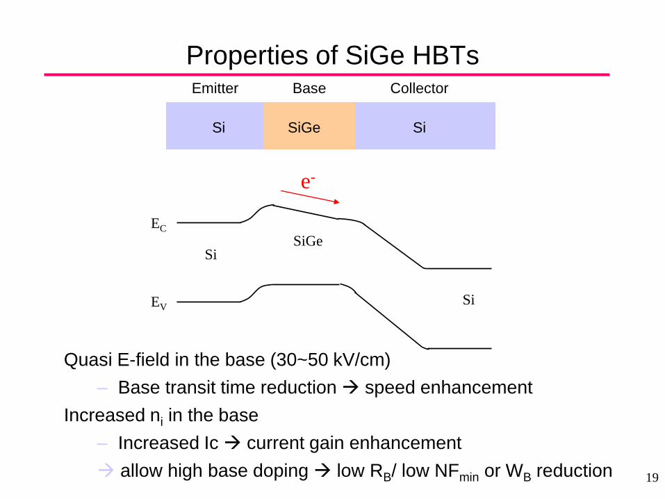
Properties of SiGe HBTs
19
Si SiGe
Si
EC
EV
e-
Quasi E-field in the base (30~50 kV/cm)
– Base transit time reduction speed enhancement
Increased ni in the base
– Increased Ic current gain enhancement
allow high base doping low RB/ low NFmin or WB reduction
Si
Emitter
SiGe Si
Base Collector
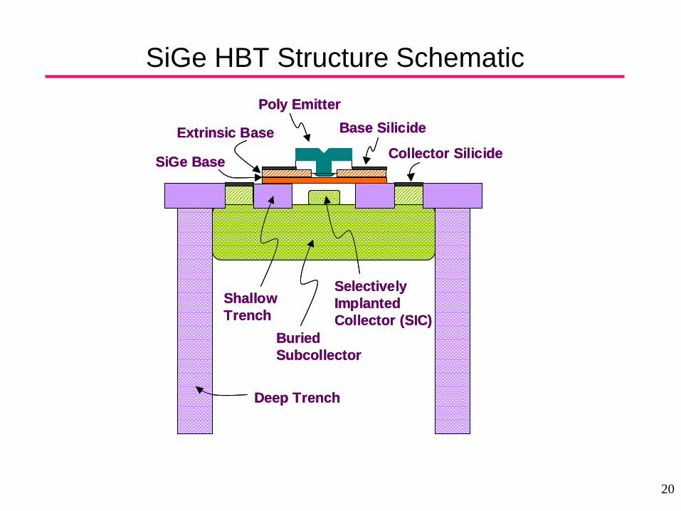
SiGe HBT Structure Schematic
SiGe Base
Deep Trench
Extrinsic Base
Poly Emitter
Selectively
Implanted
Collector (SIC)
Buried
Subcollector
Base Silicide
Shallow
Trench
Collector SilicideSiGe Base
Deep Trench
Extrinsic Base
Poly Emitter
Selectively
Implanted
Collector (SIC)
Buried
Subcollector
Base Silicide
Shallow
Trench
Collector Silicide
20
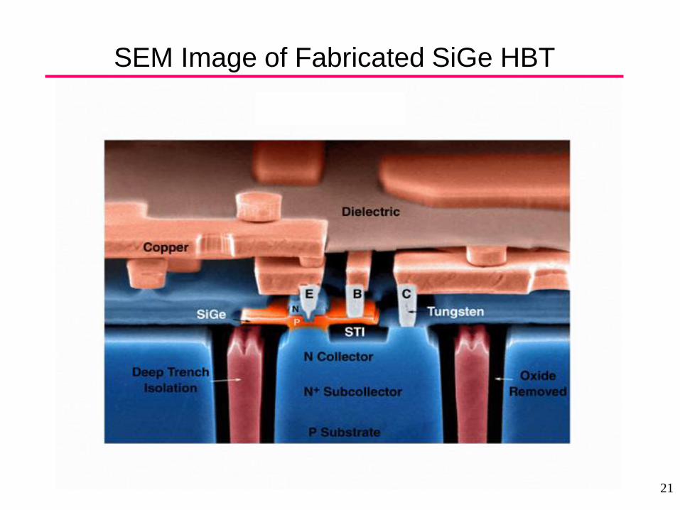
SEM Image of Fabricated SiGe HBT
21
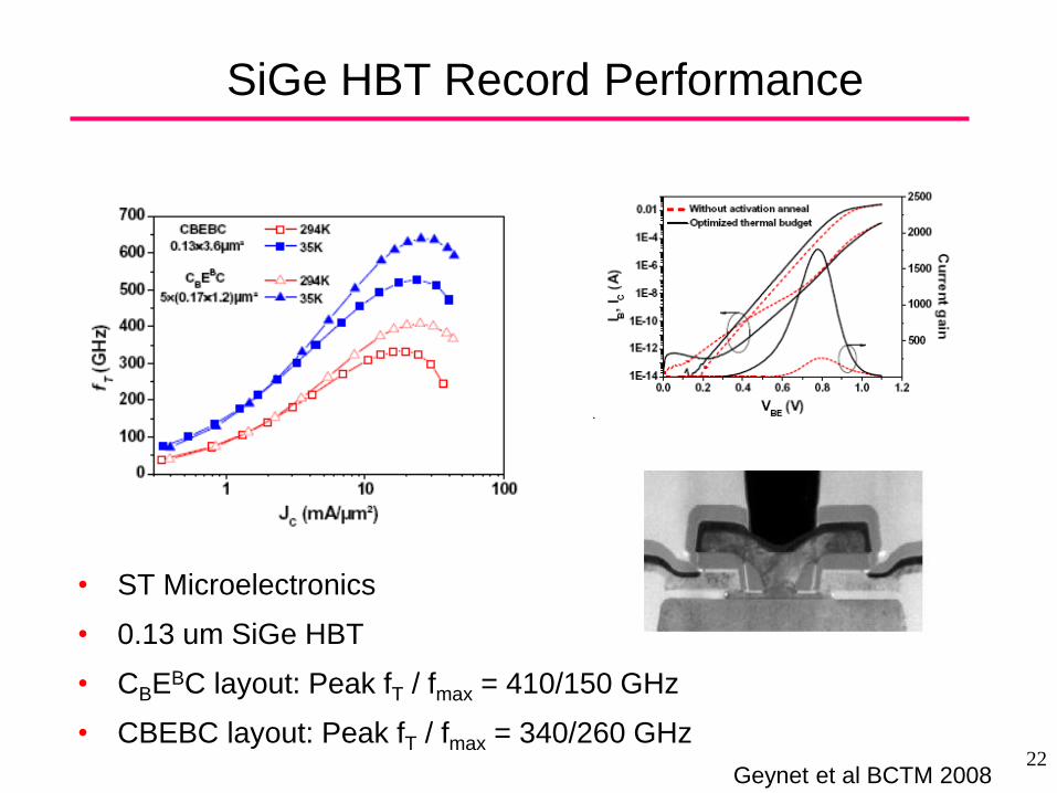
SiGe HBT Record Performance
• ST Microelectronics
• 0.13 um SiGe HBT
• CBEBC layout: Peak fT / fmax = 410/150 GHz
• CBEBC layout: Peak fT / fmax = 340/260 GHz
Geynet et al BCTM 2008 22
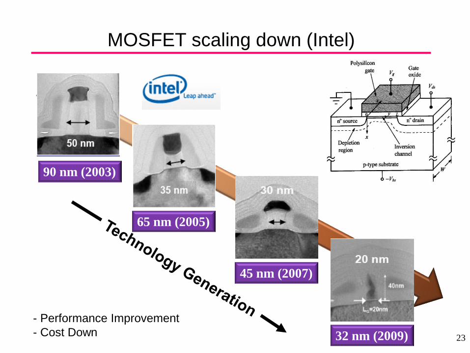
MOSFET scaling down (Intel)
- Performance Improvement
- Cost Down
90 nm (2003)
65 nm (2005)
45 nm (2007)
32 nm (2009) 23
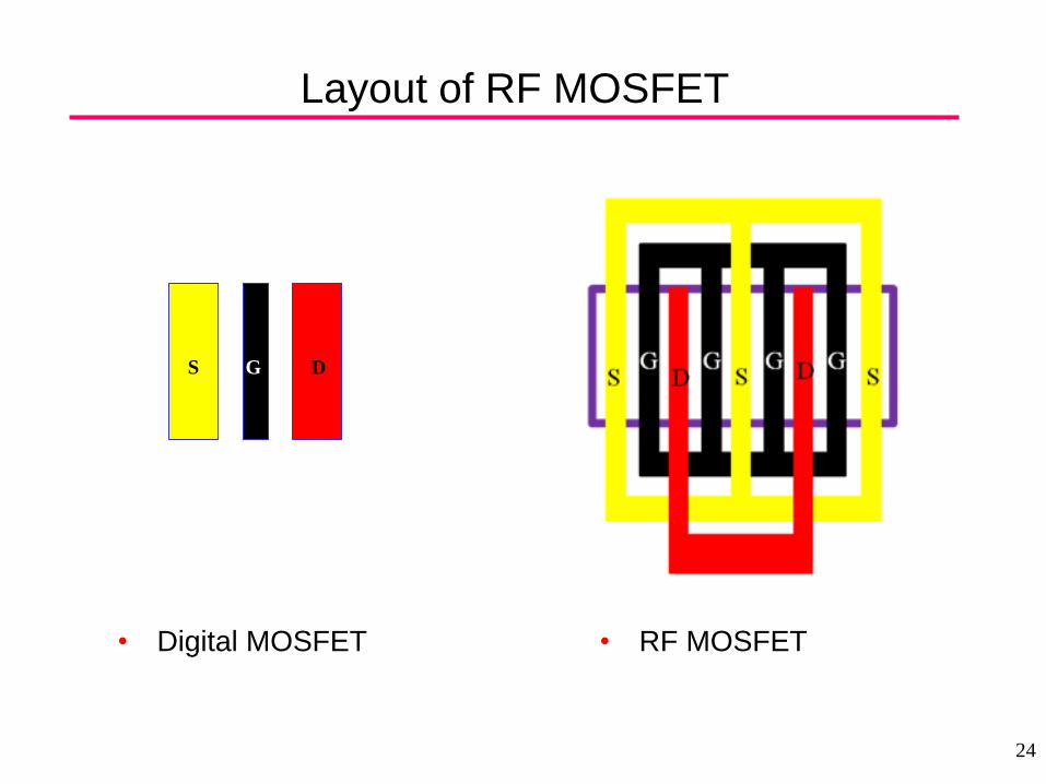
S D G
Layout of RF MOSFET
• Digital MOSFET • RF MOSFET
24
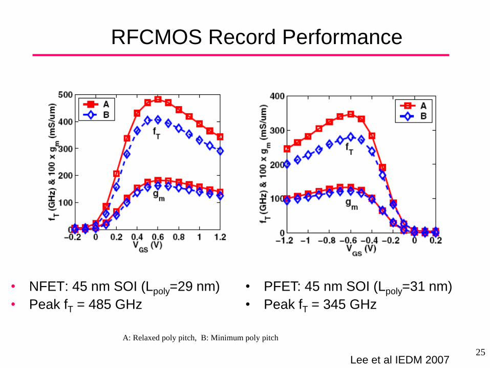
RFCMOS Record Performance
• NFET: 45 nm SOI (Lpoly=29 nm)
• Peak fT = 485 GHz
Lee et al IEDM 2007
A: Relaxed poly pitch, B: Minimum poly pitch
• PFET: 45 nm SOI (Lpoly=31 nm)
• Peak fT = 345 GHz
25
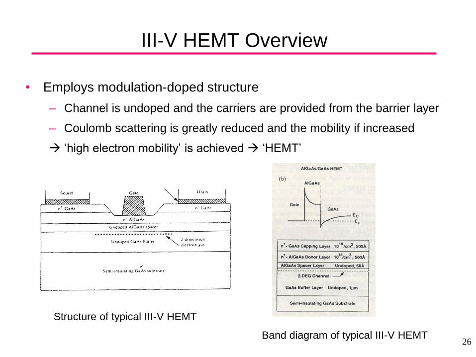
• Employs modulation-doped structure
– Channel is undoped and the carriers are provided from the barrier layer
– Coulomb scattering is greatly reduced and the mobility if increased
‘high electron mobility’ is achieved ‘HEMT’
III-V HEMT Overview
Structure of typical III-V HEMT
Band diagram of typical III-V HEMT 26
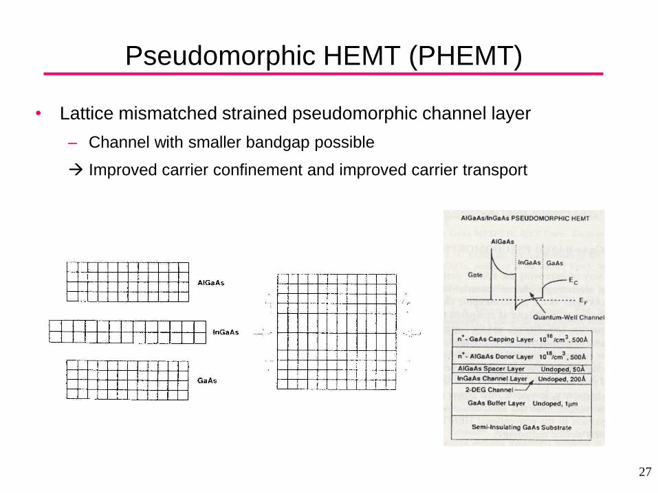
Pseudomorphic HEMT (PHEMT)
• Lattice mismatched strained pseudomorphic channel layer
– Channel with smaller bandgap possible
Improved carrier confinement and improved carrier transport
27
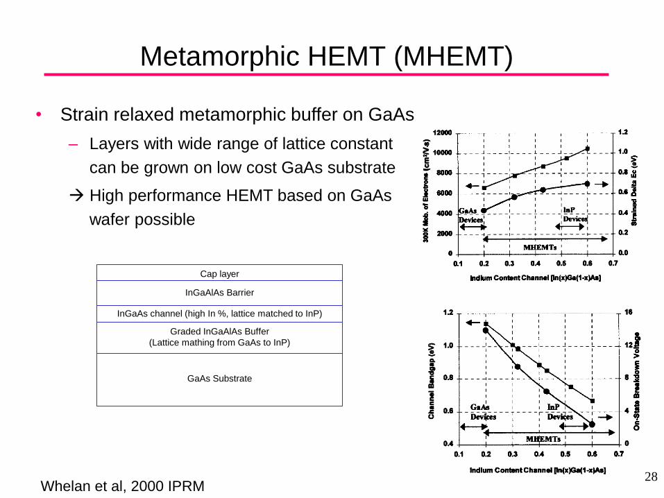
Metamorphic HEMT (MHEMT)
Whelan et al, 2000 IPRM
• Strain relaxed metamorphic buffer on GaAs
– Layers with wide range of lattice constant
can be grown on low cost GaAs substrate
High performance HEMT based on GaAs
wafer possible
GaAs Substrate
Graded InGaAlAs Buffer
(Lattice mathing from GaAs to InP)
InGaAs channel (high In %, lattice matched to InP)
InGaAlAs Barrier
Cap layer
28
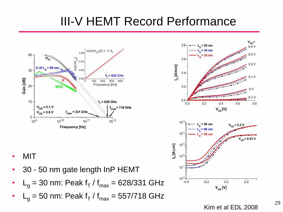
III-V HEMT Record Performance
• MIT
• 30 - 50 nm gate length InP HEMT
• Lg = 30 nm: Peak fT / fmax = 628/331 GHz
• Lg = 50 nm: Peak fT / fmax = 557/718 GHz
Kim et al EDL 2008 29
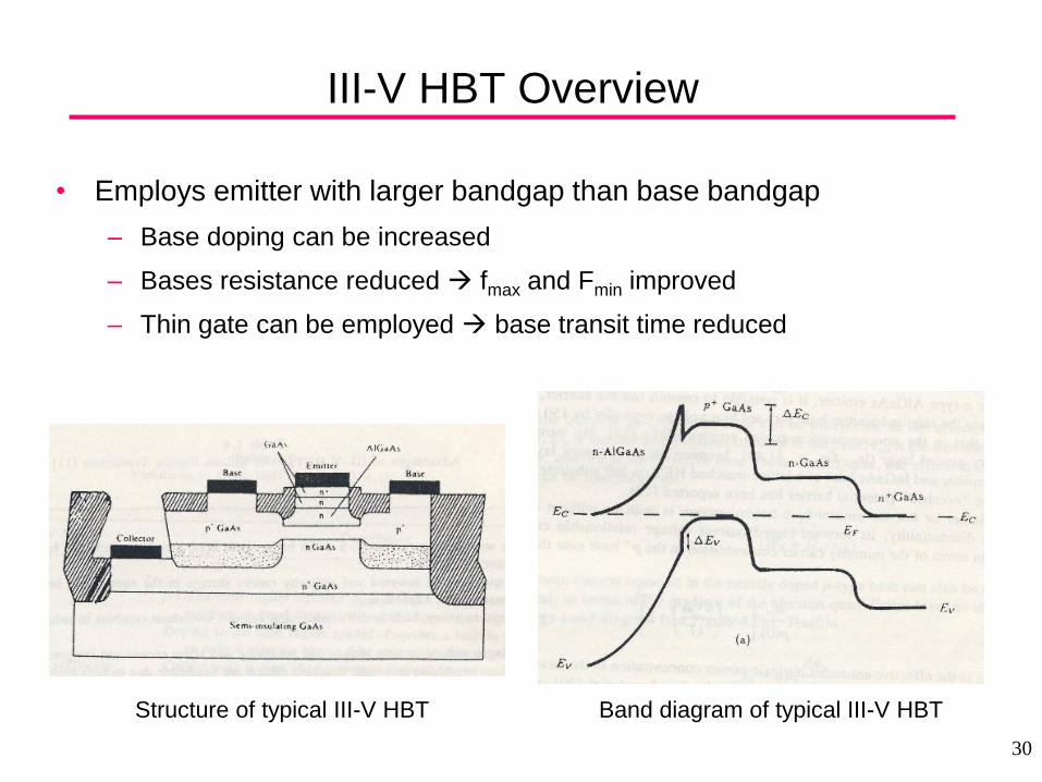
• Employs emitter with larger bandgap than base bandgap
– Base doping can be increased
– Bases resistance reduced fmax and Fmin improved
– Thin gate can be employed base transit time reduced
III-V HBT Overview
Structure of typical III-V HBT Band diagram of typical III-V HBT
30
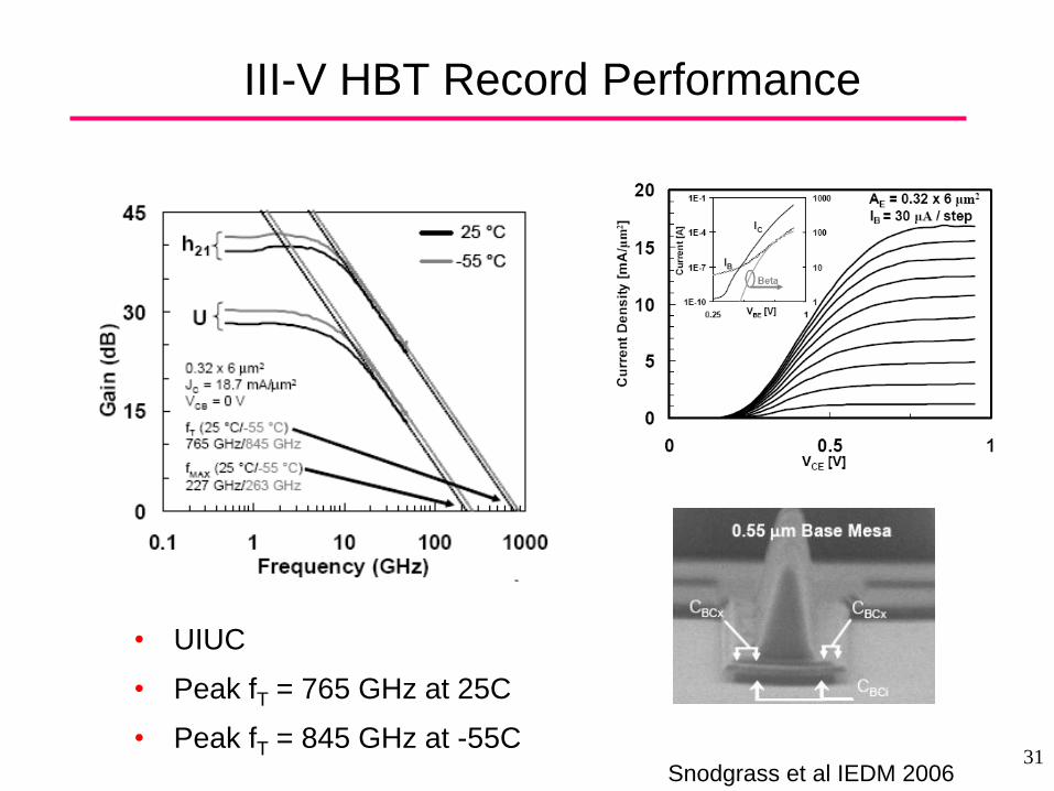
III-V HBT Record Performance
• UIUC
• Peak fT = 765 GHz at 25C
• Peak fT = 845 GHz at -55C Snodgrass et al IEDM 2006
31
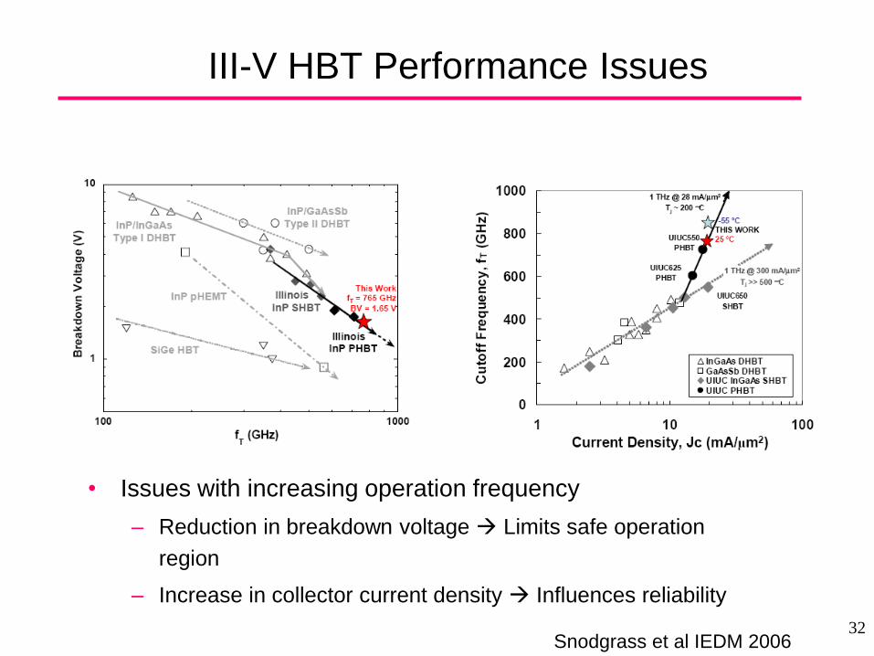
III-V HBT Performance Issues
• Issues with increasing operation frequency
– Reduction in breakdown voltage Limits safe operation
region
– Increase in collector current density Influences reliability
Snodgrass et al IEDM 2006 32
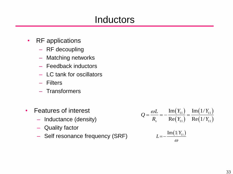
Inductors
• RF applications
– RF decoupling
– Matching networks
– Feedback inductors
– LC tank for oscillators
– Filters
– Transformers
• Features of interest
– Inductance (density)
– Quality factor
– Self resonance frequency (SRF)
11 11
11 11
Im Im 1/
Re Re 1/s
Y YLQ
R Y Y
11Im 1 YL
33
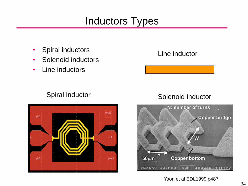
Inductors Types
• Spiral inductors
• Solenoid inductors
• Line inductors
Yoon et al EDL1999 p487
Spiral inductor Solenoid inductor
Line inductor
34
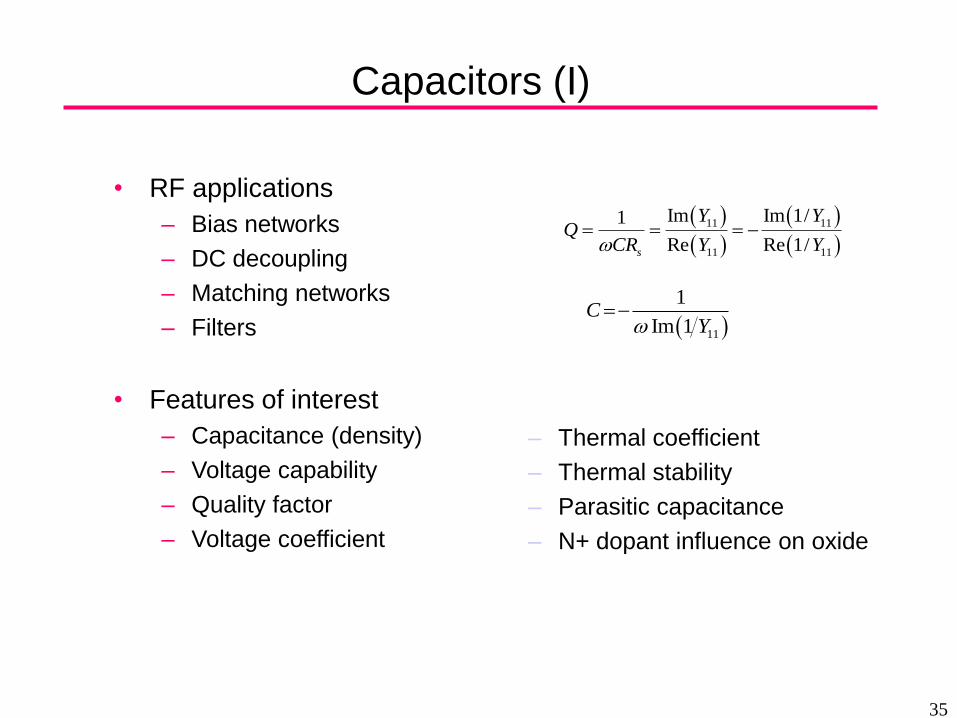
Capacitors (I)
• RF applications
– Bias networks
– DC decoupling
– Matching networks
– Filters
• Features of interest
– Capacitance (density)
– Voltage capability
– Quality factor
– Voltage coefficient
– Thermal coefficient
– Thermal stability
– Parasitic capacitance
– N+ dopant influence on oxide
11 11
11 11
Im Im 1/1
Re Re 1/s
Y YQ
CR Y Y
11
1
Im 1C
Y
35
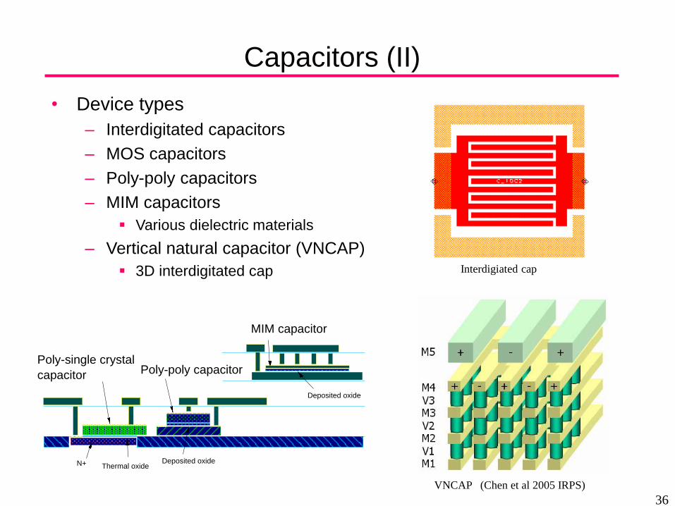
Capacitors (II)
• Device types
– Interdigitated capacitors
– MOS capacitors
– Poly-poly capacitors
– MIM capacitors
Various dielectric materials
– Vertical natural capacitor (VNCAP)
3D interdigitated cap
Poly-single crystal
capacitor Poly-poly capacitor
Thermal oxideN+ Deposited oxide
MIM capacitor
Deposited oxide
Interdigiated cap
VNCAP (Chen et al 2005 IRPS)
36
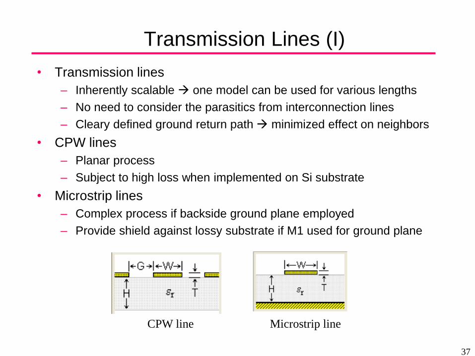
Transmission Lines (I)
• Transmission lines
– Inherently scalable one model can be used for various lengths
– No need to consider the parasitics from interconnection lines
– Cleary defined ground return path minimized effect on neighbors
• CPW lines
– Planar process
– Subject to high loss when implemented on Si substrate
• Microstrip lines
– Complex process if backside ground plane employed
– Provide shield against lossy substrate if M1 used for ground plane
Microstrip line CPW line
37
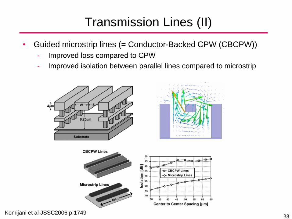
Transmission Lines (II)
• Guided microstrip lines (= Conductor-Backed CPW (CBCPW))
- Improved loss compared to CPW
- Improved isolation between parallel lines compared to microstrip
Komijani et al JSSC2006 p.1749
38
Outline
• High Frequency Applications
• High Frequency Semiconductor Devices
• High Frequency Semiconductor Circuits
39
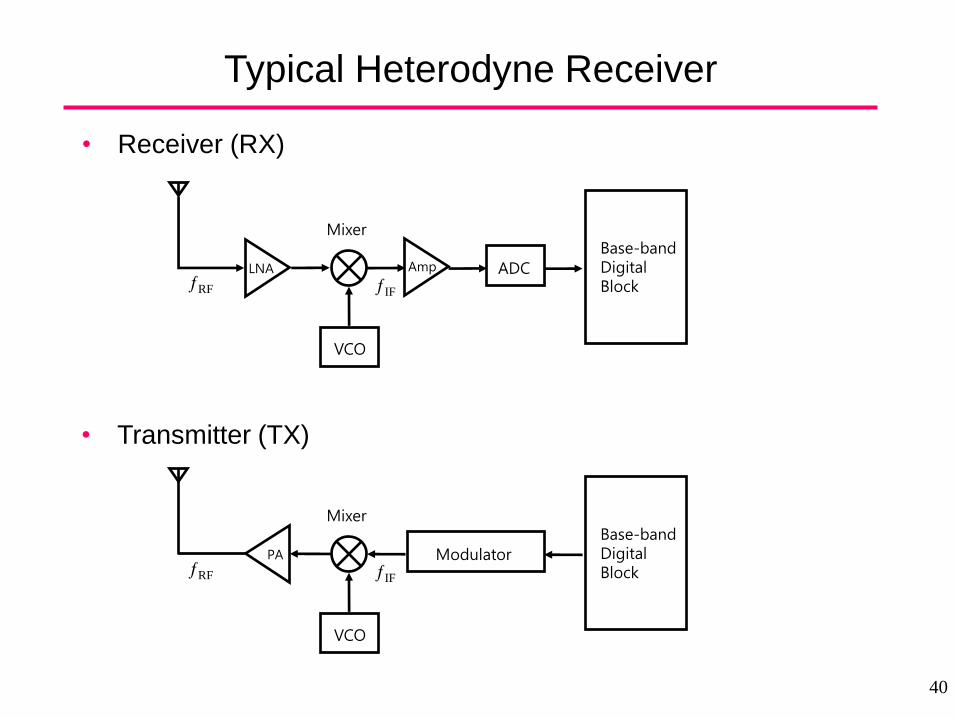
Typical Heterodyne Receiver
LNA
VCO
Base-band Digital Block ƒRF ƒIF
Mixer
Amp ADC
PA
VCO
Base-band Digital Block ƒRF ƒIF
Mixer
Modulator
• Receiver (RX)
• Transmitter (TX)
40
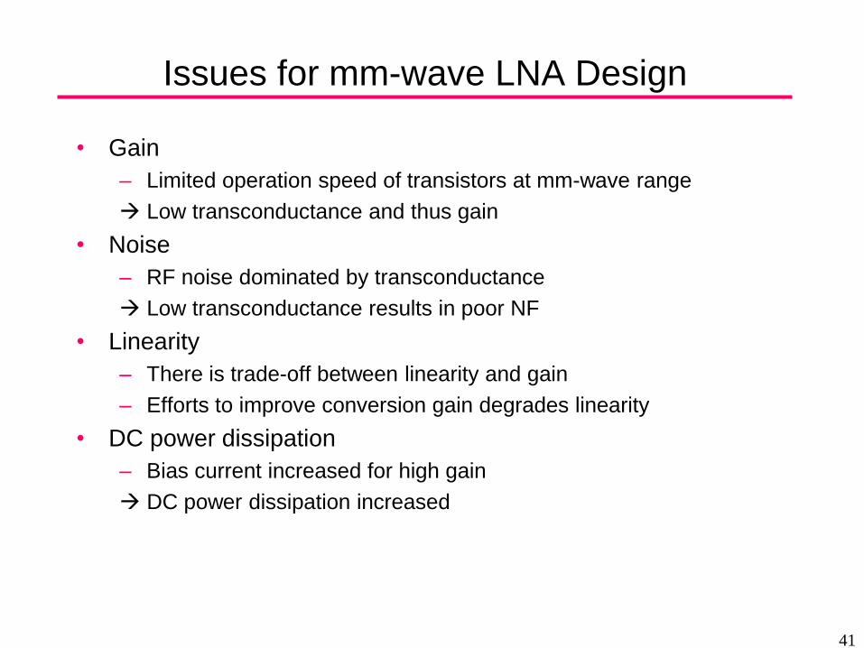
Issues for mm-wave LNA Design
• Gain
– Limited operation speed of transistors at mm-wave range
Low transconductance and thus gain
• Noise
– RF noise dominated by transconductance
Low transconductance results in poor NF
• Linearity
– There is trade-off between linearity and gain
– Efforts to improve conversion gain degrades linearity
• DC power dissipation
– Bias current increased for high gain
DC power dissipation increased
41
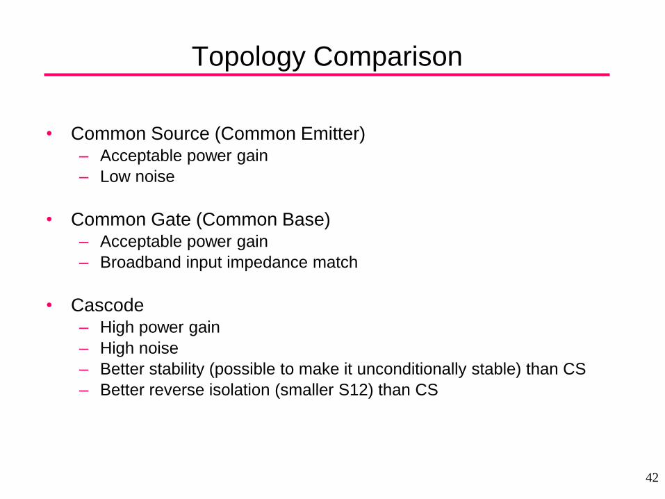
Topology Comparison
• Common Source (Common Emitter) – Acceptable power gain
– Low noise
• Common Gate (Common Base) – Acceptable power gain
– Broadband input impedance match
• Cascode – High power gain
– High noise
– Better stability (possible to make it unconditionally stable) than CS
– Better reverse isolation (smaller S12) than CS
42
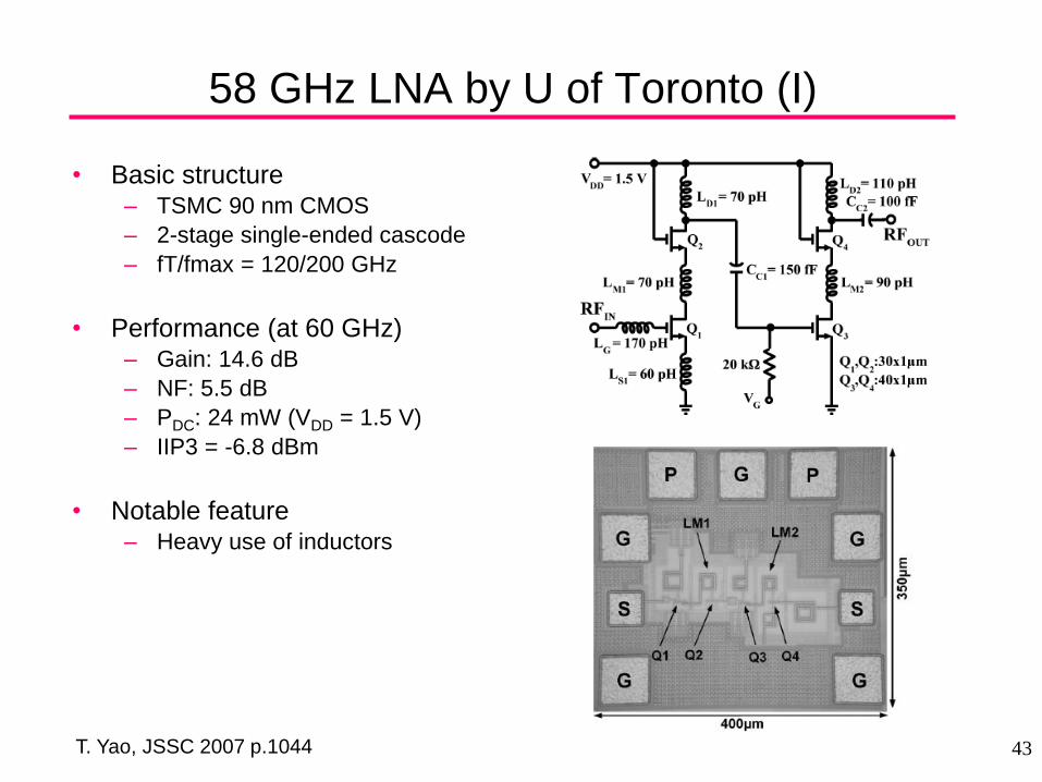
58 GHz LNA by U of Toronto (I)
• Basic structure – TSMC 90 nm CMOS
– 2-stage single-ended cascode
– fT/fmax = 120/200 GHz
• Performance (at 60 GHz) – Gain: 14.6 dB
– NF: 5.5 dB
– PDC: 24 mW (VDD = 1.5 V)
– IIP3 = -6.8 dBm
• Notable feature – Heavy use of inductors
T. Yao, JSSC 2007 p.1044 43
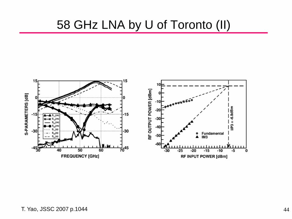
58 GHz LNA by U of Toronto (II)
T. Yao, JSSC 2007 p.1044 44
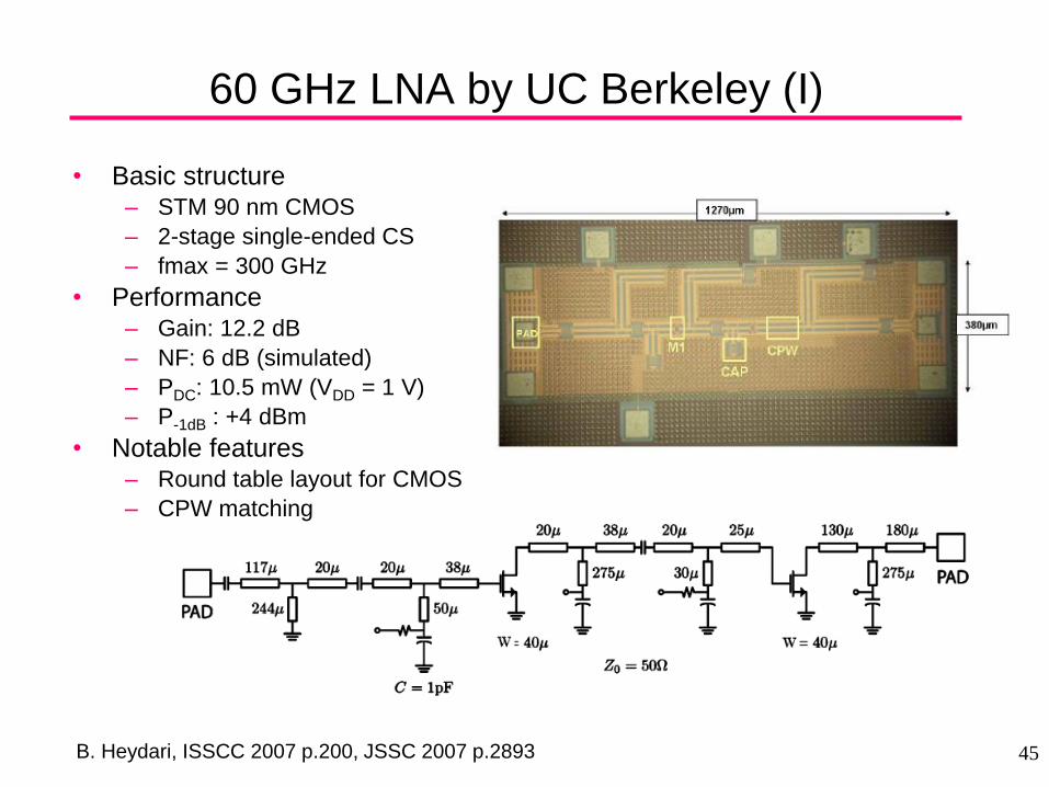
60 GHz LNA by UC Berkeley (I)
• Basic structure – STM 90 nm CMOS
– 2-stage single-ended CS
– fmax = 300 GHz
• Performance – Gain: 12.2 dB
– NF: 6 dB (simulated)
– PDC: 10.5 mW (VDD = 1 V)
– P-1dB : +4 dBm
• Notable features – Round table layout for CMOS
– CPW matching
B. Heydari, ISSCC 2007 p.200, JSSC 2007 p.2893 45
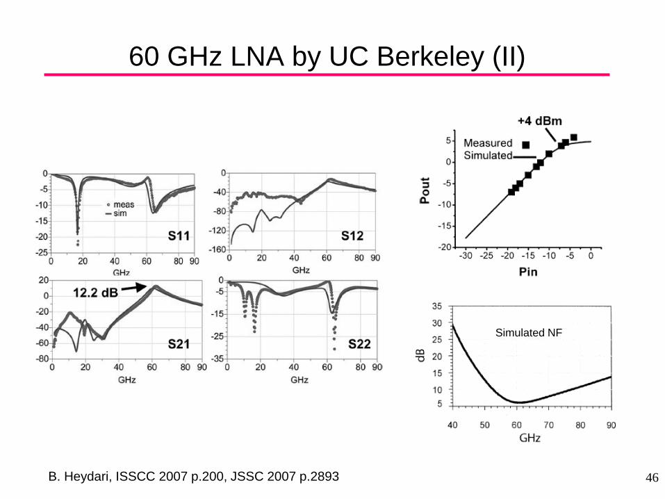
60 GHz LNA by UC Berkeley (II)
Simulated NF
B. Heydari, ISSCC 2007 p.200, JSSC 2007 p.2893 46
Issues for mm-wave VCO Design
• Phase noise
– Low Q-factor of LC tank
Dominated by the low varactor Q-factor
• Tuning range
– Capacitance from varactors only a fraction of total capacitance of
LC tank
• DC power dissipation
– Enough gm required for start-up condition
– Large bias current required for sufficient gm
• RF output power
– Limited by VDD for sufficient tail current
Trade-off with DC power dissipation
– Buffer gain limited by active device gm
47
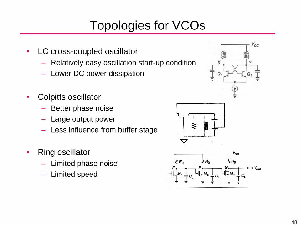
Topologies for VCOs
• LC cross-coupled oscillator
– Relatively easy oscillation start-up condition
– Lower DC power dissipation
• Colpitts oscillator
– Better phase noise
– Large output power
– Less influence from buffer stage
• Ring oscillator
– Limited phase noise
– Limited speed
48
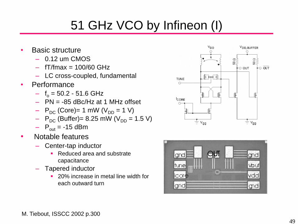
51 GHz VCO by Infineon (I)
• Basic structure – 0.12 um CMOS
– fT/fmax = 100/60 GHz
– LC cross-coupled, fundamental
• Performance – fo = 50.2 - 51.6 GHz
– PN = -85 dBc/Hz at 1 MHz offset
– PDC (Core)= 1 mW (VDD = 1 V)
– PDC (Buffer)= 8.25 mW (VDD = 1.5 V)
– Pout = -15 dBm
• Notable features
– Center-tap inductor Reduced area and substrate
capacitance
– Tapered inductor 20% increase in metal line width for
each outward turn
M. Tiebout, ISSCC 2002 p.300
49
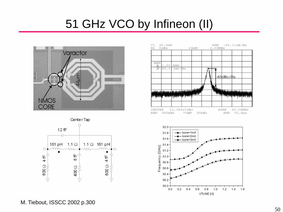
51 GHz VCO by Infineon (II)
M. Tiebout, ISSCC 2002 p.300
50
Issues for mm-wave Mixer Design
• Conversion gain
– Limited operation speed of transistors at mm-wave range
Low transconductance and thus conversion gain
• Noise
– RF noise dominated by transconductance
Low transconductance results in poor NF
• Linearity
– There is trade-off between linearity and conversion gain
– Efforts to improve conversion gain degrades linearity
• DC power dissipation
– Bias current increased for high conversion gain
DC power dissipation increased
51
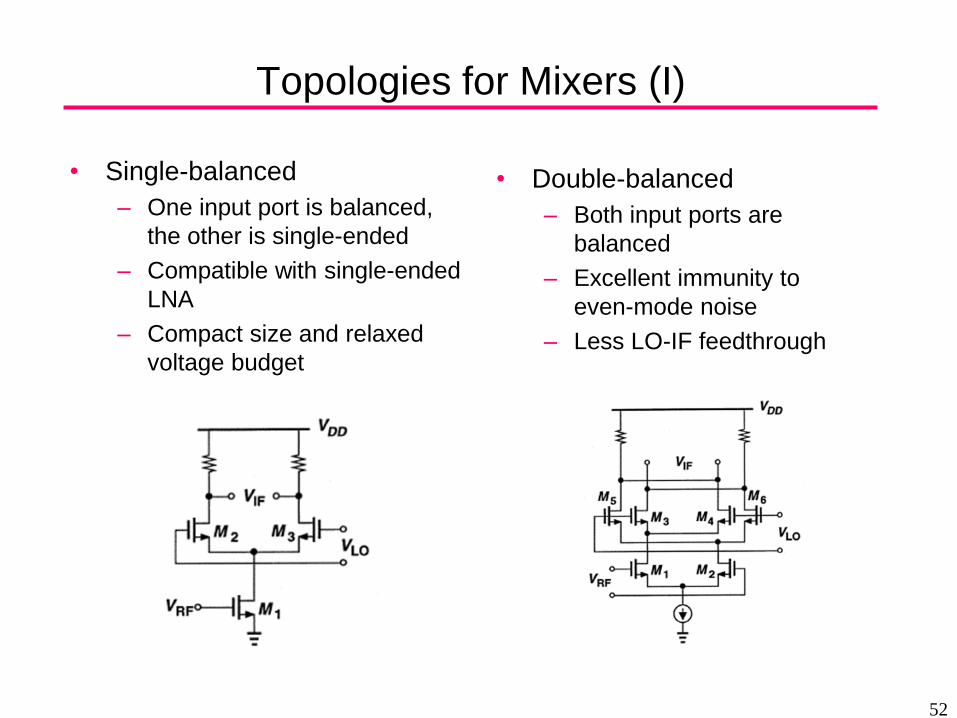
Topologies for Mixers (I)
• Single-balanced
– One input port is balanced,
the other is single-ended
– Compatible with single-ended
LNA
– Compact size and relaxed
voltage budget
• Double-balanced
– Both input ports are
balanced
– Excellent immunity to
even-mode noise
– Less LO-IF feedthrough
52
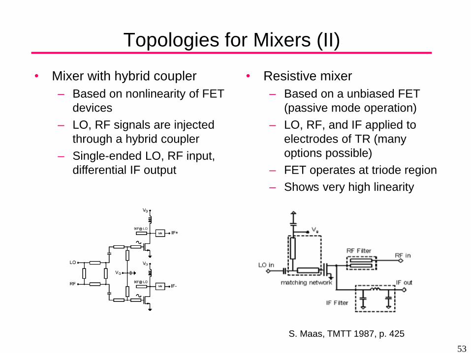
Topologies for Mixers (II)
• Resistive mixer
– Based on a unbiased FET
(passive mode operation)
– LO, RF, and IF applied to
electrodes of TR (many
options possible)
– FET operates at triode region
– Shows very high linearity
S. Maas, TMTT 1987, p. 425
53
• Mixer with hybrid coupler
– Based on nonlinearity of FET
devices
– LO, RF signals are injected
through a hybrid coupler
– Single-ended LO, RF input,
differential IF output
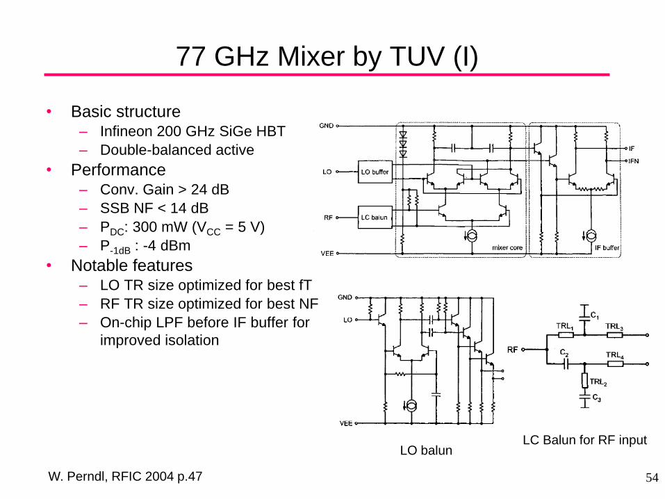
77 GHz Mixer by TUV (I)
• Basic structure – Infineon 200 GHz SiGe HBT
– Double-balanced active
• Performance – Conv. Gain > 24 dB
– SSB NF < 14 dB
– PDC: 300 mW (VCC = 5 V)
– P-1dB : -4 dBm
• Notable features – LO TR size optimized for best fT
– RF TR size optimized for best NF
– On-chip LPF before IF buffer for
improved isolation
W. Perndl, RFIC 2004 p.47
LO balun LC Balun for RF input
54
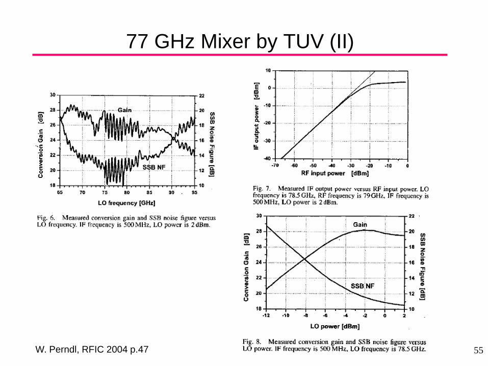
77 GHz Mixer by TUV (II)
W. Perndl, RFIC 2004 p.47 55
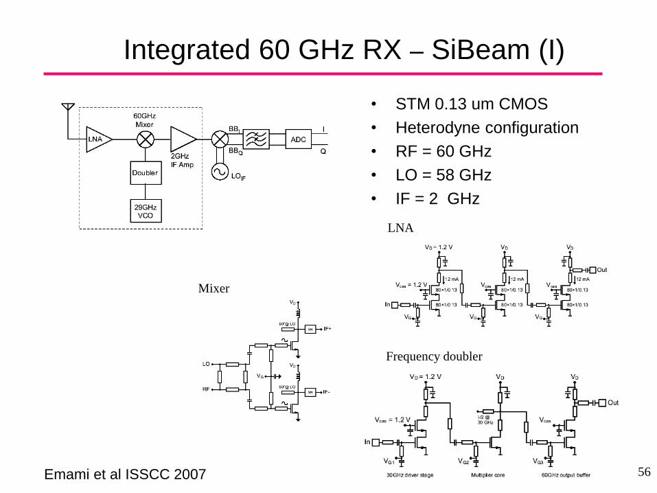
Integrated 60 GHz RX – SiBeam (I)
• STM 0.13 um CMOS
• Heterodyne configuration
• RF = 60 GHz
• LO = 58 GHz
• IF = 2 GHz
LNA
Mixer
Frequency doubler
Emami et al ISSCC 2007 56
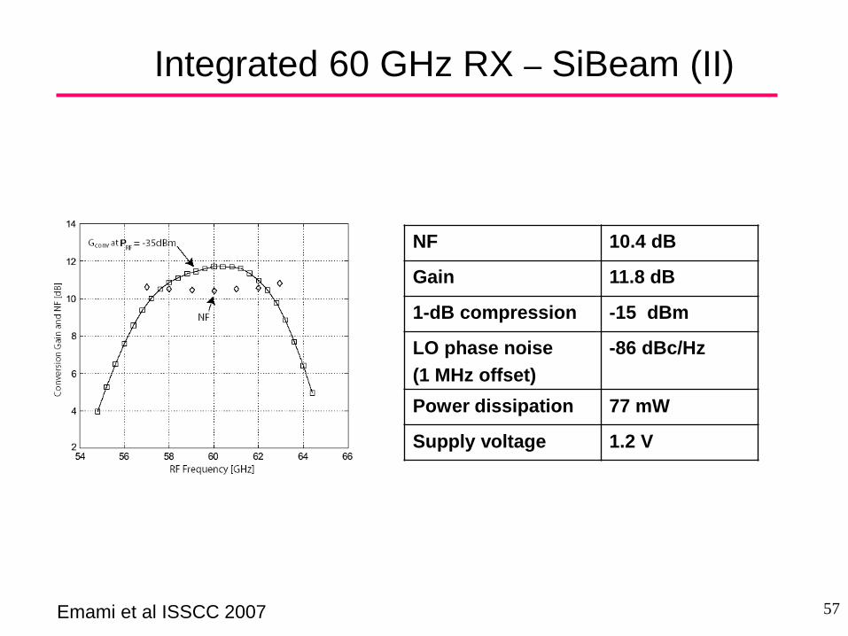
Integrated 60 GHz RX – SiBeam (II)
NF 10.4 dB
Gain 11.8 dB
1-dB compression -15 dBm
LO phase noise
(1 MHz offset)
-86 dBc/Hz
Power dissipation 77 mW
Supply voltage 1.2 V
Emami et al ISSCC 2007 57
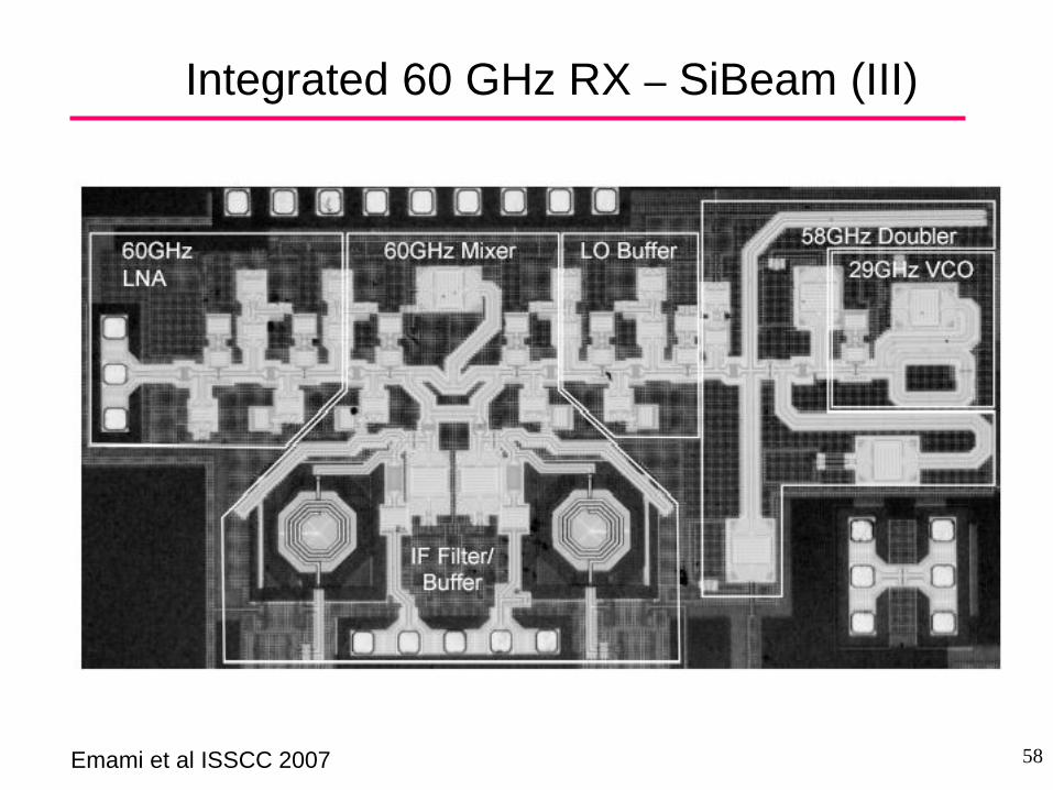
Integrated 60 GHz RX – SiBeam (III)
Emami et al ISSCC 2007 58
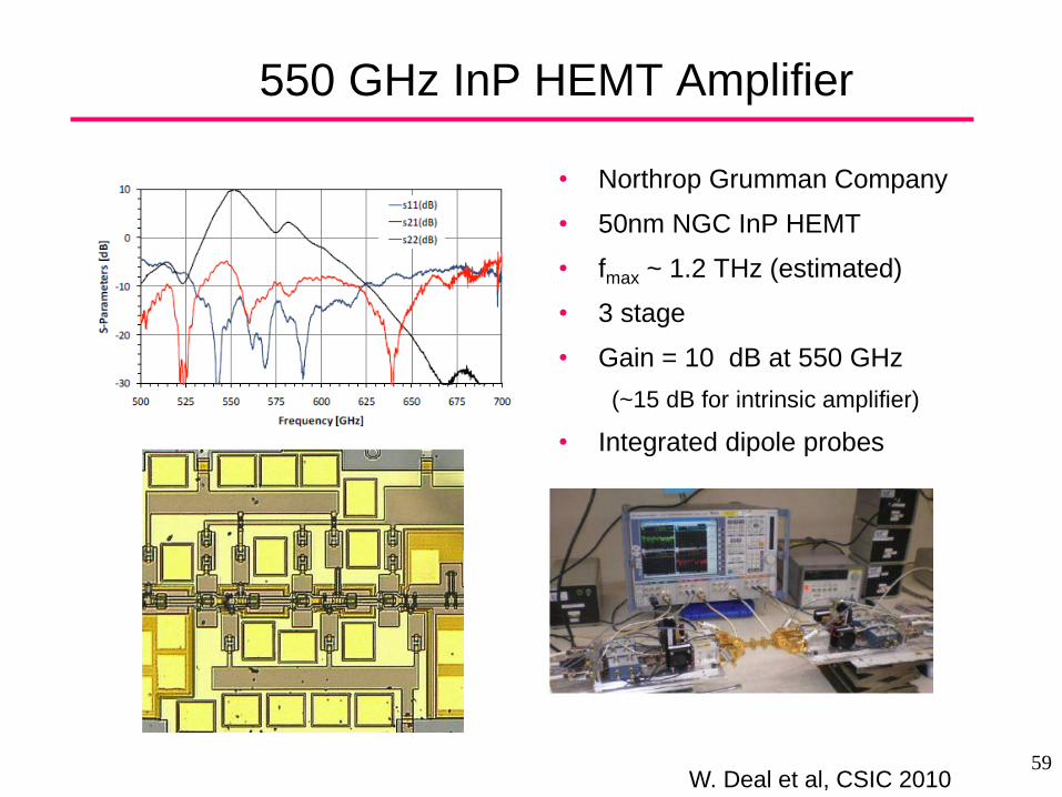
550 GHz InP HEMT Amplifier
• Northrop Grumman Company
• 50nm NGC InP HEMT
• fmax ~ 1.2 THz (estimated)
• 3 stage
• Gain = 10 dB at 550 GHz
(~15 dB for intrinsic amplifier)
• Integrated dipole probes
W. Deal et al, CSIC 2010 59
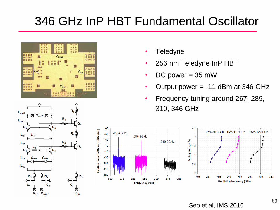
346 GHz InP HBT Fundamental Oscillator
• Teledyne
• 256 nm Teledyne InP HBT
• DC power = 35 mW
• Output power = -11 dBm at 346 GHz
• Frequency tuning around 267, 289,
310, 346 GHz
Seo et al, IMS 2010 60
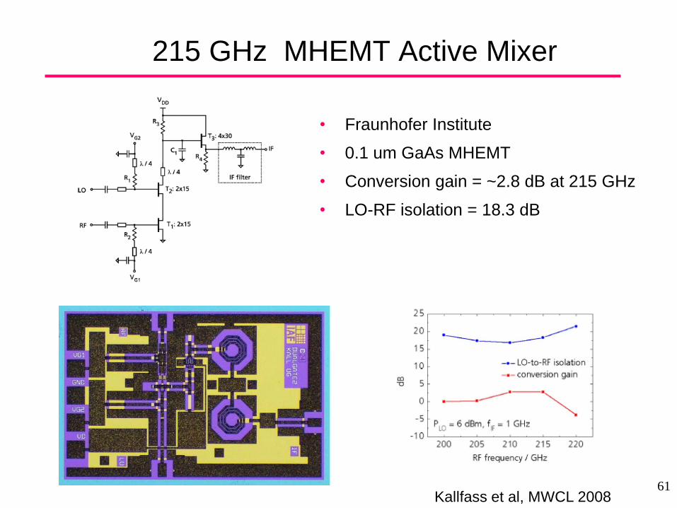
215 GHz MHEMT Active Mixer
• Fraunhofer Institute
• 0.1 um GaAs MHEMT
• Conversion gain = ~2.8 dB at 215 GHz
• LO-RF isolation = 18.3 dB
Kallfass et al, MWCL 2008 61