Embed Size (px)
Citation preview
High Gain Planar Antenna Structures for Ka-band
Applications
Kiran Dnyandeo Phalak
A Thesis
in
The Department
Of
Electrical and Computer Engineering
Presented in Partial Fulfillment of the requirements
For the degree of Master in Applied Science (Electrical Engineering) at
Concordia University
Montreal, Quebec, Canada
April 2014
© Kiran Phalak 2014

CONCORDIA UNIVERSITY
SCHOOL OF GRADUATE STUDIES
This is to certify that the thesis prepared
By: Kiran Dnyandeo Phalak
Entitled: “High Gain Planar Antenna Structures for Ka-band Applications”
and submitted in partial fulfillment of the requirements for the degree of
Master of Applied Science
Complies with the regulations of this University and meets the accepted standards with
respect to originality and quality.
Signed by the final examining committee:
________________________________________________ Chair
Dr. M. Z. Kabir
________________________________________________ Examiner, External
Dr. H. Akbari, (BCEE) To the Program
________________________________________________ Examiner
Dr. T. Denidni
________________________________________________ Supervisor
Dr. A. Sebak
Approved by: ___________________________________________
Dr. W. E. Lynch, Chair
Department of Electrical and Computer Engineering
____________20_____ ___________________________________
Dr. C. W. Trueman
Interim Dean, Faculty of Engineering
and Computer Science
iii
Abstract
High Gain Planar Antenna Structures for Ka-band Applications
Kiran Phalak
Antennas are an essential part of a communication system as they control a coverage area of
the signal. The millimeter wave band has the potential to offer numerous radio applications
which require the large bandwidth channels. Due to the current cellular subscribers’ demand of
higher data rates, even cellular communication is expected to move in millimeter wave
communications at Ka band of 26.5 GHz to 40 GHz. However, millimeter waves are sensitive to
the high degree of atmospheric and oxygen absorption losses. This challenge of the millimeter
wave communication can be tackled by employing high gain antennas. In addition, modern
electronic products require compact handheld devices to offer the user-friendly system as well
as capture the market. Therefore, planar antenna structures are apt for these communication
systems.
In this thesis, two antenna structures are presented at the Ka band for millimeter wave
communications. Initially, four element patch antenna is presented for high gain in the
broadside direction. Patch elements are excited using an aperture coupling from 50Ω microstrip
line. Air-gap cavity is used to improve the impedance bandwidth of the design. This structure
obtains a relatively moderate impedance bandwidth of 4.6%. The proposed four-element patch
antenna exhibits a flat gain over an operating band with 13.8 dB gain at the design frequency.
The antenna achieves a wide beamwidth of 700 in H plane. In addition, side lobe levels in E and
H planes are -14.5 dB and 23 dB respectively. For the second prototype, an Antipodal Fermi-
Linear Tapered Slot Antenna (AFLTSA) is presented to achieve the wide impedance bandwidth

iv
with high flat gain for endfire radiation. Substrate Integrated waveguide (SIW) technique is
utilized to feed the AFLTSA which reduces insertion losses of the structure. Fermi-Dirac
distributed curve in conjunction with a linear curve for a tapered slot increases the coupling of
the electric field from a substrate integrated waveguide to the tapered slot. Knife edge
rectangular corrugation profile is used at edges of AFLTSA in order to reduce the side lobes and
cross polarization levels of radiation pattern. The proposed structure achieves the wide
impedance bandwidth to support requirements for high data rate channels. Measurement
results from a fabricated prototype exhibit a flat gain over an entire operating frequency band
with 16.4 dB gain at 28 GHz. The wide impedance bandwidth is achieved with return loss below
15 dB. Proposed structure has low side lobe levels of -13.9 dB in H plane and -19.5 dB in E plane.
In addition, it offers a low cross polarization level of -22 dB.

v
Acknowledgement
First and foremost, I would like to convey my thanks to my supervisor Dr. Abdel Sebak for his
guidance throughout this work. His timely consultation and advises have a huge part in framing
this research work. I am grateful to him to offer the opportunity to work with him in the field of
millimeter wave antenna designing.
My sincere thanks to Dr. Ahmed Kishk and Dr. Robert Paknys for their engrossing teaching and
critical technical guidance about electromagnetics during the Master of Engineering program. I
am thankful for my friend and PhD aspiring, Zouhair Briqech, for his collaboration with one of
the important sections of this thesis work. His expertise and experience in an antenna
fabrication and measurement systems has been more than handful for me to complete my work
within time. I am gratified to get valuable tips and technical understanding from my fellow
electromagnetic group students. I obliged to them for keeping the sportive atmosphere in the
premises which helped me to focus and work ardently as well.
My graduation could not have happened without moral and all kind of support from my parents.
I am deeply thankful to my brother for believing in my abilities and interest. Without their
encouragement and support this would not have been possible.

vi
Table of Contents
List of Abbreviations----------------------------------------------------------------------------------------ix
List of Figures-------------------------------------------------------------------------------------------------xi
List of Tables-------------------------------------------------------------------------------------------------xv
Chapter 1
Introduction----------------------------------------------------------------------------------1
1.1 Introduction to the Wireless Communication------------------------------------------------1
1.2 Motivation-------------------------------------------------------------------------------------------- 3
1.2.1 Need for Millimeter Wave Communication--------------------------------3
1.2.2 5G Cellular Communication at Ka band-------------------------------------6
1.3 Thesis Objective------------------------------------------------------------------------------------- 9
1.4 Thesis Organization------------------------------------------------------------------------------- 10
Chapter 2
Literature Overview----------------------------------------------------------------------11
2.1 Evolution of Millimeter Wave Communication------------------------------------------ 11
2.2 Antennas for Millimeter Wave Communication---------------------------------------- 12
2.2.1 Horn Antennas----------------------------------------------------------------------- 13
2.2.2 Lens Antennas------------------------------------------------------------------------ 14
2.2.3 Dielectric Rod Antennas------------------------------------------------------------16
2.2.4 Slot Antennas------------------------------------------------------------------------- 17
2.2.5 Dielectric Resonator Antennas--------------------------------------------------- 18
2.2.6 Microstrip Antennas---------------------------------------------------------------- 19

vii
2.2.7 Tapered Slot Antennas--------------------------------------------------------------20
2.2.8 Comparison of various Millimeter wave Antennas--------------------------22
2.3 Numerical techniques for full-wave analysis--------------------------------------------- 24
2.3.1 Finite Element Method-------------------------------------------------------------25
2.3.2 Finite Integration Technique------------------------------------------------------28
2.4 Summary------------------------------------------------------------------------------------------ 29
Chapter 3
Four Element Aperture Coupled Patch Antenna--------------------------------- 30
3.1 Microstrip antenna----------------------------------------------------------------------------- 30
3.1.1 Introduction--------------------------------------------------------------------------- 30
3.1.2 Feeding techniques------------------------------------------------------------------ 31
3.2 Design of Four Element Patch Radiator ---------------------------------------------------32
3.2.1 Design of Microstrip line feed-----------------------------------------------------32
3.2.2 Design of Coupling Aperture-------------------------------------------------------33
3.2.3 Design of Patch Element------------------------------------------------------------35
3.2.4 Improvement of Gain using Multiple Elements-------------------------------36
3.3 Proposed Structure and Design Parameters----------------------------------------------37
3.4 Parametric Study-------------------------------------------------------------------------------- 39
3.4.1 Lower Dielectric Substrate--------------------------------------------------------- 39
3.4.2 Effect of air-gap cavity---------------------------------------------------------------40
3.5 Prototype and Results--------------------------------------------------------------------------40
3.5.1 Single Element Patch Antenna---------------------------------------------------- 40
3.5.2 Four Element Patch Antenna------------------------------------------------------ 42

viii
Chapter 4
Antipodal Fermi-Linear Tapered Slot Antenna------------------------------------46
4.1 Design Methodology--------------------------------------------------------------------------- 46
4.1.1 Design of Feed Section---------------------------------------------------------------47
4.1.2 Design of Tapered Slot with Corrugated Edges--------------------------------50
4.2 Parametric analysis-----------------------------------------------------------------------------53
4.2.1 Distance between SIW and slot opening--------------------------------------53
4.2.2 Separation between End Points of Fermi Curve-----------------------------54
4.2.3 Width of Corrugation-------------------------------------------------------------- 54
4.2.4 Blending the Corrugated Edges--------------------------------------------------55
4.3 Prototypes and Measurement Setup-------------------------------------------------------56
4.4 Results and Discussion----------------------------------------------------------------------- 60
Chapter 5
Conclusion----------------------------------------------------------------------------------64
5.1 Conclusion---------------------------------------------------------------------------------------64
5.2 Contribution------------------------------------------------------------------------------------ 65
5.3 Future Scope------------------------------------------------------------------------------------66
References-------------------------------------------------------------------------------------------------------------------67

ix
List of Abbreviations
AFLTSA Antipodal Fermi Linear Tapered Slot Antenna
ALTSA Antipodal Linear Tapered Slot Antenna
CAD Computer Aided Design
CBCPW Conductor Backed Coplanar waveguide
CDMA Code Division Multiple Access
CEPT European Conference of Postal and Telecommunications Administrations
CPW Coplanar Waveguide
DRA Dielectric Resonator Antenna
FCC Federal Communications Commission
FEM Finite Element Method
FIT Finite Integration Technique
FM Frequency Modulation
GCPW Grounded Coplanar Waveguide
GPS Global Positioning System
HF High Frequency
HSPA High Speed Package Access
ISM Industrial Scientific Medical
ITU International Telecommunication Union
LF Low Frequency
LTCC Low temperature co-fired ceramic
LTE Long Term Evolution
LTSA Linear Tapered Slot Antenna

x
LWA Leaky Wave Antenna
MIC Microwave Integrated Circuit
MIMO Multiple Input Multiple Output
MMID Millimeter Identification
MMW Millimeter waves
PCB Printed Circuit Board
PTFE Poly Tetra Fluoro Ethylene
QTEM Quasi Transverse Electromagnetic
RADAR Radio Detection and Ranging
RFID Radio Frequency Identification
SiP System-in-Package
SIRC Substrate Integrated Radial Coaxial
SIW Substrate Integrated Waveguide
SoP System-on-Package
TDMA Time Division Multiple Access
TE Transverse Electric
TM Transverse Magnetic
TSA Tapered Slot Antenna
UHF Ultra High Frequency
UTD Uniform Theory of Diffraction
VHF Very High Frequency
VoIP Voice over Internet Protocol
WPAN Wireless Personal Area Network

xi
List of Symbols
B Magnetic flux density
BW Bandwidth
c Speed of light / speed of EM waves in free space
C Channel capacity
E Electric field intensity
f Operating frequency
H Magnetic field intensity
J Electric current density
Lant Length of antenna
R Distance between transmitter and receiver
S/N Signal to noise ratio
εr Relative permittivity
λg Guided wavelength
λ0 Free space wavelength
λ Operating wavelength

xii
List of Figures
Figure 1.1 Block diagram of wireless communication------------------------------------------ 2
Figure 1.2 Rapid growth in mobile subscribers--------------------------------------------------- 6
Figure 1.3 Curve for atmospheric attenuation at millimeter waves------------------------ 8
Figure 1.4 Curves for attenuation due to rain at millimeter waves------------------------- 8
Figure 2.1 MMW horn antenna designs for (a) broadside and (b) endfire radiation--- 13
Figure 2.2 (a) Half Maxwell fish-eye and (b) luneberg lens antenna structures for
MMW applications------------------------------------------------------------------------
15
Figure 2.3 Different shapes of dielectric rod antennas---------------------------------------- 16
Figure 2.4 Slot antenna structures (a) transverse slots on substrate integrated
waveguide (b) slot director to enhance radiation pattern-----------------------
17
Figure 2.5 (a) Pentagonal and (b) cylindrical dielectric resonator antenna structures- 18
Figure 2.6 Printed antenna structures: (a) Yagi array and (b) circular polarized
microstrip antenna------------------------------------------------------------------------
19
Figure 2.7 Balance microstrip line fed Tapered slot antenna (a) Top view (b) bottom
view-------------------------------------------------------------------------------------------
20
Figure 2.8 Electric field line orientation for (a) unbalanced microstrip line (b)
Balanced microstrip line (c) antipodal tapered slot-------------------------------
21
Figure 2.9 SIW fed ALTSA------------------------------------------------------------------------------ 22
Figure 2.10 A subdivision of a region using finite elements------------------------------------ 26
Figure 2.11 Irregular triangular element with three nodes------------------------------------- 26
Figure 2.12 (a) Staircase-Hexahedron type meshing (b) Tetrahedron meshing (c)
Allocation of voltages and flux on hexahedron element-------------------------
29

xiii
Figure 3.1 Microstrip patch antenna---------------------------------------------------------------- 30
Figure 3.2 Various feeding techniques for patch antennas: (a) Coaxial probe feed (b)
microstrip line feed (c) Aperture coupled feed (d) Proximity feed------------
31
Figure 3.3 Single element aperture couple patch antenna layers--------------------------- 32
Figure 3.4 (a) Microstrip Line (b) electric field line distribution for microstrip line----- 33
Figure 3.5 Open ended transmission line and current distribution over the line-------- 34
Figure 3.6 Effect on impedance matching of (a) slot length and (b) open stub length- 34
Figure 3.7 Fringing effect in patch antenna (a) Top view (b) side view--------------------- 36
Figure 3.8 Array factor for four elements uniformly fed equidistant array--------------- 37
Figure 3.9 Proposed four element patch antenna structure (a) in 3D and (b) in layer
separation view----------------------------------------------------------------------------
38
Figure 3.10 Effect of a lower dielectric substrate material on (a) return loss (b) gain
and front to back ratio-------------------------------------------------------------------
39
Figure 3.11 Effect of air-gap cavity on a single element patch antenna performance--- 40
Figure 3.12 Return loss and gain of a single element patch antenna using CST and
HFSS-------------------------------------------------------------------------------------------
41
Figure 3.13 (a) E plane and (b) h plane radiation pattern of the single element patch-- 41
Figure 3.14 Prototype for Four element patch antenna structure---------------------------- 42
Figure 3.15 Return Loss and gain response of four element patch antenna using CST
and HFSS and measurements-----------------------------------------------------------
42
Figure 3.16 (a) E plane and (b) H plane radiation pattern for proposed structure-------- 44
Figure 3.17 (a) E plane and (b) H plane radiation patterns of proposed antenna
structure at 27.3, 28 and 28.7 GHz----------------------------------------------------
44
Figure 3.18 Total efficiency of the proposed antenna structure------------------------------ 45

xiv
Figure 4.1 Proposed AFLTSA structure with design parameters----------------------------- 47
Figure 4.2 Substrate integrated waveguide design--------------------------------------------- 48
Figure 4.3 Orientation of Electric field lines in (a) rectangular waveguide and (b)
microstrip line------------------------------------------------------------------------------
49
Figure 4.4 Tapered microstrip to SIW transition with design parameters----------------- 50
Figure 4.5 Return loss study for microstrip-to-SIW transition design parameters Lt
and Wt----------------------------------------------------------------------------------------
50
Figure 4.6 (a) Vivaldi (b) Linear (c) Fermi shaped Tapered Slot Antenna------------------ 51
Figure 4.7 Design A, B and C of AFLTSA with different corrugation profile---------------- 52
Figure 4.8 Effect of sp on return loss and gain of AFLTSA------------------------------------- 53
Figure 4.9 Effect of d on realized gain of the AFLTSA------------------------------------------- 54
Figure 4.10 Effect of corrugation width on E and H plane side lobe level------------------- 55
Figure 4.11 (a) Blended corrugations and (b) effect of corrugation on side lobe levels
of the AFLTSA-------------------------------------------------------------------------------
55
Figure 4.12 Top and bottom views of (a) Design A, (b) Design B and (c) Design C-------- 57
Figure 4.13 Schematic for radiation pattern and gain measurement setup---------------- 57
Figure 4.14 (a) Anechoic chamber having measurement setup (b) antenna under test- 58
Figure 4.15 Return loss and gain response of Design C (b) E and H plane radiation
pattern of Design C at 28 GHz----------------------------------------------------------
58
Figure 4.16 2D plane cut view of the Design C showing an electric field distribution---- 59
Figure 4.17 (a) Return loss and gain response of Design A (b) E and H plane radiation
pattern of Design A at 28 GHz----------------------------------------------------------
59
Figure 4.18 (a) Return loss and gain response of Design B (b) E and H plane radiation
pattern of Design B------------------------------------------------------------------------
60

xv
Figure 4.19 Radiation patterns of proposed AFLTSA design B structure at (a) 26 GHz
and (b) 33 GHz------------------------------------------------------------------------------
60
Figure 4.20 Electric field distribution at aperture of the AFLTSA design A, B and C------ 61
Figure 4.21 E and H plane side lobe level difference for the AFLTSA design A, B and C- 62
Figure 4.22 Comparison of total efficiency of AFTSA designs---------------------------------- 62

xvi
List of Tables
Table 2.1 Gain and size comparison for Millimeter wave Antennas--------------------- 23
Table 3.1 Design parameters and their dimensions for proposed structure----------- 38
Table 3.2 Properties of utilized dielectric mediums------------------------------------------ 39
Table 3.3 Comparison of proposed antenna with broadside radiating antennas in
literature----------------------------------------------------------------------------------
45
Table 4.1 Design parameters and dimensions of AFLTSA----------------------------------- 56
Table 4.2 Comparison of proposed antenna with endfire radiating antennas in
literature-----------------------------------------------------------------------------------
63

- 1 -
Chapter 1
1.1 Introduction to the Wireless Communication
Wireless communications have been a focus of researchers all over the globe ever since Marconi
built the first radio system in 1895 [1]. Just a thought of transferring data from one place to
another by means of oscillating electromagnetic waves, motivated researchers from various
fields to explore the field of wireless data transfer. As a result, wireless data transfer is not only
limited for a communication purpose, but also being used in medical, surveillance, amateur
radio, robotics and radio broadcast fields’ applications. One of the largest application of wireless
communication is a cellular communication. Similarly, a satellite communication is also a major
wireless field as it offers educational, security, communication advantages. Other examples
include short distance wireless data transfer by the Bluetooth standard and radio frequency
identification (RFID) that allows tracking as well as data acquisition from tagged remote objects
[2]. Radio detection and ranging (RADAR) finds its way into military, air traffic control, and
surveillance applications [3]. In the medical field, this principle is used for a cancer detection [4]
and cardiac monitoring [5].
In general, wireless communication among points can be divided into three main stages, as
shown in Fig. 1.1: transmission, propagation and reception. Transmission stage deals with
processing of baseband or low frequency (LF) signal. A transmitter modulates LF data on a high
frequency carrier signal and launches it in the space. A modulated signal propagates through the
space in the form of electromagnetic waves. During the propagation, a signal deals with

- 2 -
turbulent man-made or natural noise sources which attenuates and deforms the signal. At the
receiving end, this signal is captured by the receiver which filters out unwanted signals. The
original data is recovered by the demodulation process at the receiver. As spurious effects
during the propagation cannot be controlled, design of effective transmission and reception
system is essential for reliable wireless communication [6].
Figure 1.1 Block diagram of wireless communication
At both ends of a wireless link, the task of radiating and capturing the electromagnetic energy in
and from the desired direction is performed by an antenna. An antenna itself is a passive
reciprocal device. Therefore, whenever a transmitting antenna is discussed, the discussion
always implies for a receiving antenna as well, unless specifically stated. A performance of any
antenna can be described by the values of its various parameters. Antenna parameters include
directivity, efficiency, beamwidth, impedance bandwidth, side lobe level, polarization and input
impedance [7]. In addition, cost, weight and size of antenna can also be critical for certain
applications. Any handheld device operating on a battery, thus, needs a power efficient antenna
such that its battery life will last longer. Satellite communication requires a narrow beam
antenna whereas broadcast communication requires wide beam antennas. Dual polarization is
required to establish two individual communication channels with the same antenna system.
Hence, antenna design is solely dependent on the application in which it is to be used.
- 3 -
1.2 Motivation
1.2.1 Need for Millimeter Wave Communication
The rapid growth in radio communication industries and applications has clustered the
electromagnetic spectrum. Therefore, wireless channel allocation in each country is regulated
by national organizations such as Federal Communications Commission (FCC), Industry Canada,
European Conference of Postal and Telecommunications Administrations (CEPT) [6]. Although
this ensured that no chaos can be caused by the communication interference, scarcity of
available wireless channels still continues to be a big challenge faced by wireless industries. As
most of the current wireless systems operate at HF (3MHz to 30MHz), VHF (30MHz to 300MHz)
and UHF (300MHz to 3GHz) bands, the electromagnetic spectrum at these bands is crowded [8].
In addition, the relative bandwidth of communication channels at these bands is in the range of
few megahertz. According to Shannon–Hartley theorem, given by (1.1), a channel capacity (C) is
directly dependent on the bandwidth (BW) of a communication channel and the signal to noise
ratio (S/N) [9]. Therefore, applications which require higher data speed cannot operate
satisfactorily at these low bandwidth channels.
( ) (1.1)
The most logical solution for this problem is shifting wireless applications towards higher
frequencies. Typically, the electromagnetic spectrum in the range of 30 GHz to 300 GHz (i.e.
wavelength of 10 mm to 1 mm) is referred as the millimeter wave (MMW) frequency band. It
can be also defined Extremely high frequency (EHF) band [3].

- 4 -
Millimeter wave characteristics have numerous advantages from the communication system
point-of-view as discussed ahead:
Smaller wavelengths allow the design of small size components, resulting in a compact
system.
For same physical size, narrow beamwidth can be obtained using MMW antennas as
operating wavelength is smaller [3].
The bandwidth available at MMW is extremely large, hence wide bandwidth channels
can be allocated in MMW frequencies [10].
Wide band spread spectrum capability for reduced multipath and clutter [3].
Availability of certain high attenuation bands which has potential for highly secure short
distance communication [10].
Along with advantages, MMW characteristics also exhibit certain disadvantages for
communications applications.
According to the Friis transmission equation, a free space loss factor, given in (1.2),
increases with a square of the operating signal frequency [11].
(
) (
)
(1.2)
An atmospheric attenuation, caused by rain, scattering, water vapor and oxygen
absorption at MMW frequency, limits the communication range [10].
Smaller wavelength results in small component size, resulting in a necessity of highly
precise production processing.
Narrow beamwidth offered by MMW can be a problem for a large volume search radar
[3].

- 5 -
Although MMW communication had much lesser exploitation than microwave communication,
MMW communication has been utilized and proposed for following applications for many years
[3][10].
1. Secure military communication
2. Radio astronomy and meteorological satellites
3. Weather and military radars
4. Millimeter wave imaging
5. Remote sensing applications
6. Gigabit wireless communications
7. Wireless HDTV
One of the biggest challenges of MMW communications is to reduce the cost of the system. As
component size gets smaller at higher operating frequency range, processing techniques of this
precision are expensive, resulting in high cost of complete systems. In addition, due to small
wavelength MMW components are sensitive to edge diffraction as compared to microwave
range components [12]. Furthermore, most of the standard values mentioned in datasheets of
materials available in the market are given for microwave frequencies. Their properties differ
from the specification which makes it challenging to design the MMW components. Various
technologies which are being proposed at MMW are still to be well established in the industry.
Last but not the least, the most fearsome challenge at MMW communication is ever increasing
atmospheric attenuation. It is a challenge to design high gain antennas to nullify effects of the
atmospheric attenuation [10].
Nevertheless, a detailed experimental study of a non-linearity of an atmospheric loss and
research in modern technologies can help in tackling these challenges to utilize MMWs which
- 6 -
offer the large availability of communication channels with wide bandwidth. Hence, this thesis is
concerned about antennas for the MMW communication and its application in an outdoor
communication.
1.2.2 5G Cellular Communication at Ka band
Since early 1980s, when analog Frequency Modulation (FM) technology based cellular service
was introduced as the first generation mobile communication system [13], the world has seen a
rapid exponential growth in number mobile device users. Over four decades since the first
generation was deployed, wireless communication industry has seen Time Division Multiple
Access (TDMA), Code Division Multiple Access (CDMA), High Speed Packet Access (HSPA), Voice
over Internet Protocol (VoIP) and Long Term Evolution (LTE) technologies which kept
transforming cellular communication through various technological generations [14].
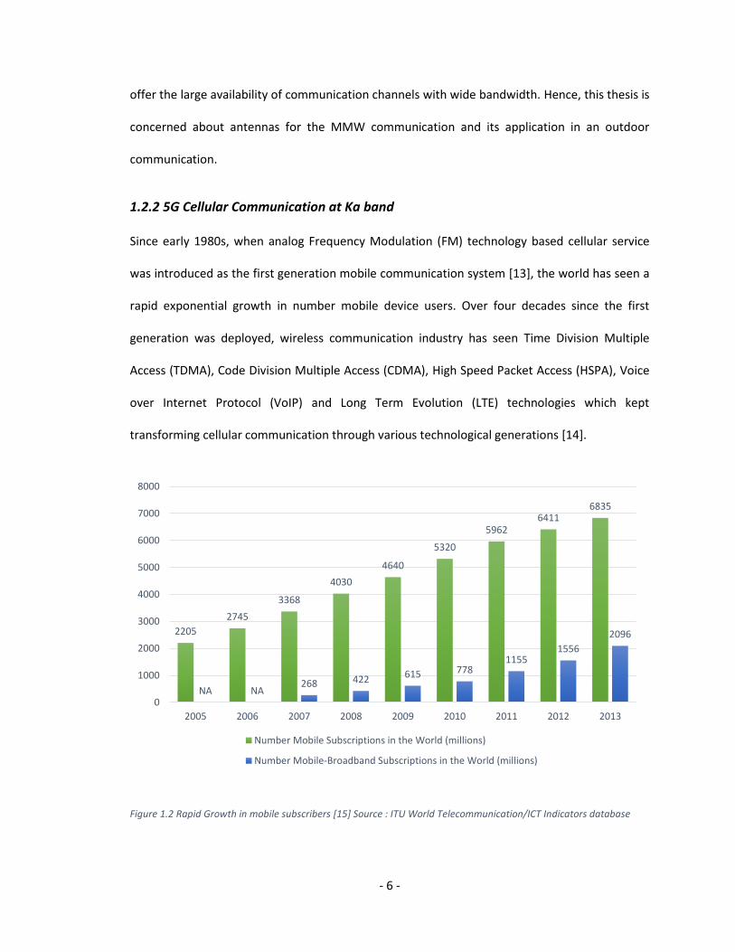
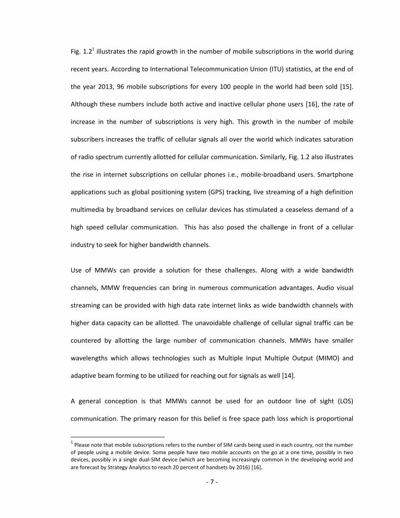
Figure 1.2 Rapid Growth in mobile subscribers [15] Source : ITU World Telecommunication/ICT Indicators database
2205
2745
3368
4030
4640
5320
5962 6411
6835
NA NA 268 422 615 778
1155 1556
2096
0
1000
2000
3000
4000
5000
6000
7000
8000
2005 2006 2007 2008 2009 2010 2011 2012 2013
Number Mobile Subscriptions in the World (millions)
Number Mobile-Broadband Subscriptions in the World (millions)
- 7 -
Fig. 1.21 illustrates the rapid growth in the number of mobile subscriptions in the world during
recent years. According to International Telecommunication Union (ITU) statistics, at the end of
the year 2013, 96 mobile subscriptions for every 100 people in the world had been sold [15].
Although these numbers include both active and inactive cellular phone users [16], the rate of
increase in the number of subscriptions is very high. This growth in the number of mobile
subscribers increases the traffic of cellular signals all over the world which indicates saturation
of radio spectrum currently allotted for cellular communication. Similarly, Fig. 1.2 also illustrates
the rise in internet subscriptions on cellular phones i.e., mobile-broadband users. Smartphone
applications such as global positioning system (GPS) tracking, live streaming of a high definition
multimedia by broadband services on cellular devices has stimulated a ceaseless demand of a
high speed cellular communication. This has also posed the challenge in front of a cellular
industry to seek for higher bandwidth channels.
Use of MMWs can provide a solution for these challenges. Along with a wide bandwidth
channels, MMW frequencies can bring in numerous communication advantages. Audio visual
streaming can be provided with high data rate internet links as wide bandwidth channels with
higher data capacity can be allotted. The unavoidable challenge of cellular signal traffic can be
countered by allotting the large number of communication channels. MMWs have smaller
wavelengths which allows technologies such as Multiple Input Multiple Output (MIMO) and
adaptive beam forming to be utilized for reaching out for signals as well [14].
A general conception is that MMWs cannot be used for an outdoor line of sight (LOS)
communication. The primary reason for this belief is free space path loss which is proportional
1 Please note that mobile subscriptions refers to the number of SIM cards being used in each country, not the number
of people using a mobile device. Some people have two mobile accounts on the go at a one time, possibly in two devices, possibly in a single dual-SIM device (which are becoming increasingly common in the developing world and
are forecast by Strategy Analytics to reach 20 percent of handsets by 2016) [16].
- 8 -
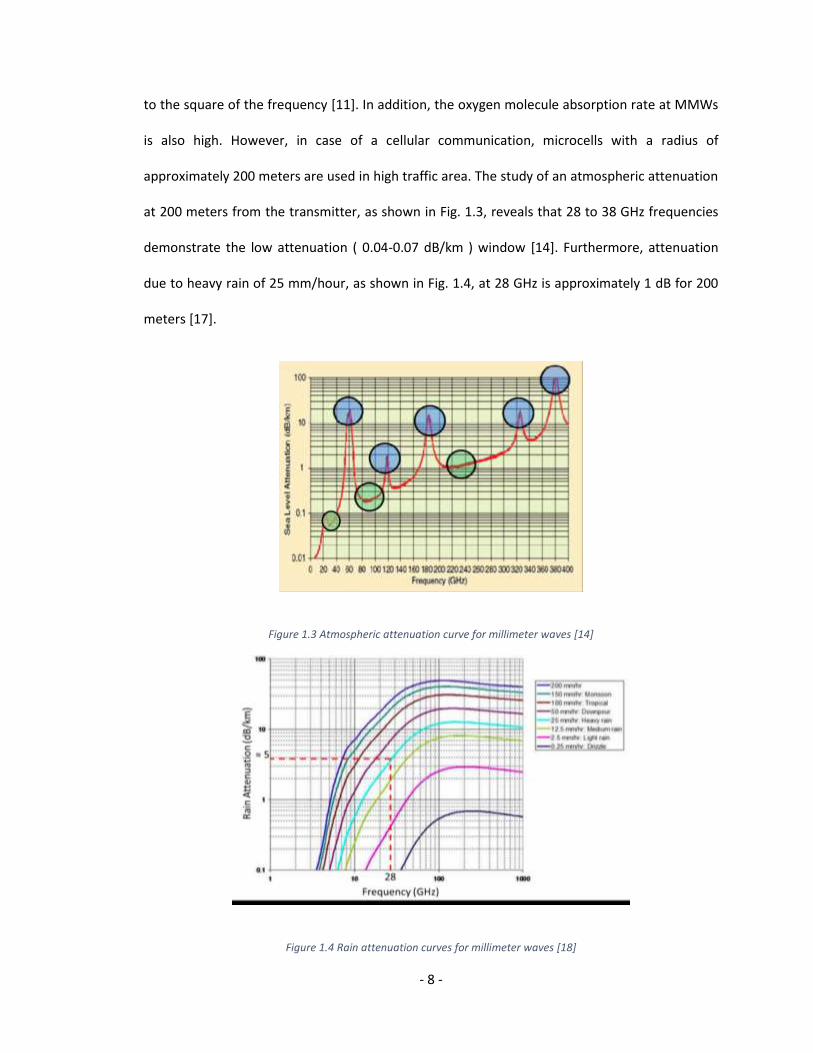
to the square of the frequency [11]. In addition, the oxygen molecule absorption rate at MMWs
is also high. However, in case of a cellular communication, microcells with a radius of
approximately 200 meters are used in high traffic area. The study of an atmospheric attenuation
at 200 meters from the transmitter, as shown in Fig. 1.3, reveals that 28 to 38 GHz frequencies
demonstrate the low attenuation ( 0.04-0.07 dB/km ) window [14]. Furthermore, attenuation
due to heavy rain of 25 mm/hour, as shown in Fig. 1.4, at 28 GHz is approximately 1 dB for 200
meters [17].
Figure 1.3 Atmospheric attenuation curve for millimeter waves [14]
Figure 1.4 Rain attenuation curves for millimeter waves [18]
- 9 -
An antenna is an essential component to establish the wireless communication between two or
more terminals. In case of cellular communication, base station antennas are used to offer
coverage in cellular sectors. The principle function of base station antennas is to increase the
coverage area. Therefore, critical design parameters for a cellular base station antenna are
azimuth beamwidth and high gain. An azimuth angle is tilted from the normal towards the
ground to improve the signal strength in a vicinity of the base station tower. This tilt in an
azimuth angle can be achieved mechanically, electronically or by the combination of both [19].
High gain and wide beamwidth are required to achieve large coverage area. However, antenna
beamwidth and gain are reciprocal to each other. Directivity of an antenna is typically increased
by focusing the beam in narrow zone, hence the half power beam width is smaller. Therefore,
multiple elements of high gain antenna are used to achieve this wide azimuth beamwidth [20].
These studies clearly identify the solution for a 5G cellular communication beyond 2025 lies with
MMWs at 28 and 38 GHz. High gain, planar, low cost antenna structures are required for point-
to-point or point-to-multipoint communication applications at Ka band of 26.5 GHz to 40 GHz.
1.3 Thesis Objective
This thesis is concerned about design of high gain compact antennas at Ka-band with focus on
planar structures. The high gain requirement is mainly to address the atmospheric attenuation
associated with MMW wireless communications. As cellular antenna structures operate in cell
design structure, maximum front-to-back ratio is desired. Another objective of the thesis is to
obtain a wide impedance bandwidth to support high data rate channels. Lower side lobe levels
are desired as it will facilitate reduction in interference. The size of an antenna should be smaller
so that it can be used in compact devices. Antenna elements are proposed for endfire and

- 10 -
broadside radiations. These elements can be used in a fixed multibeam array antenna to obtain
the required azimuth bandwidth [20].
1.4 Thesis Organization
Chapter 2 reviews the literature of a millimeter wave communication from the early applications
of a millimeter wave communication to its rise in various fields. The further section focuses on
various technologies and antenna structures which are utilized to obtain high gain at MMWs. In
depth discussion is also carried out for substrate integrated waveguide technology and tapered
slot antenna technology which are utilized in this thesis. The chapter ends with a discussion on
numerical techniques behind the simulation technology used for solving electromagnetic
problems.
Chapter 3 presents the design of a broadside radiating four-element patch array antenna.
Design methodology and working principle of the microstrip patch antenna are discussed.
Furthermore, measurement results for this antenna are presented. Parametric study and
simulation procedure are also discussed. The chapter concludes with comparison of results with
previously proposed antenna structures.
Chapter 4 presents the endfire radiating antipodal fermi linear tapered slot antenna (AFLTSA).
The design methodology is presented together with different parametric studies using full wave
simulation CAD tools. An AFLTSA prototype and its measurement method and results are also
presented. Simulated and measured results are compared.
Chapter 5 presents the conclusion of the thesis’s work. It also recommends some future
activities to be followed for completion of base station antenna design.
- 11 -
Chapter 2
2.1 Evolution of Millimeter Wave Communication
Although the first MMW communication system had been designed by Jagadish chandra Bose
before 1900 [21], it had not been popular for industrial or communication applications because
only a large wavelength communication was preferred for long distance communication. Recent
growth in the interest for the MMW communication has been triggered by the lack of available
spectrum at lower frequencies. Furthermore, approximately 7 GHz of the unlicensed ISM band is
allotted at 60 GHz millimeter waves in all countries [10]. Therefore, a large amount of the
literature about MMW communication is focused at 60 GHz ISM band.
Early advancement in MMW communication had been in the area of RADAR applications.
Smaller wavelength and narrow beamwidth, which could only be achieved at MMWs, were
beneficial to obtain greater resolution with precision in target tracking, detection application.
Additionally, it facilitates the higher angular resolution for area mapping application. The higher
gain potential of high frequency antennas assists in detecting and locating small objects. At
MMW, even a lower radial velocity of object results in higher Doppler shift. Hence, MMW radar
has the higher detection capability for moving targets. MMW radars are used for military,
weather forecast, air and marine traffic control, surveillance and radio astronomy applications
[22].
- 12 -
Chipless millimeter wave identification (MMID) at 30 GHz was reported in [23]. At MMW,
smaller size enables the design of a small tag antenna and a compact reader module as compare
to the RFID system. Furthermore, chipless MMID reduces the cost of the system as a chip or
integrated circuit is not required [23]. MMWs provide a deeper range than infrared or visible
region as they penetrate through wood, clothes. Moreover, they provide better spatial
resolution and compact system than microwave region. Therefore, MMWs are suitable for
imaging applications [24]. Consequently, MMW imaging systems have also received a wide
attention. In modern world of terrorist threats, MMW imaging can be used for a hidden object
or weapon detection [25].
On the other hand, higher frequency, wide unlicensed band (of 7 GHz) and permission of high
power transmission make 60 GHz MMW band most suitable for a gigabit wireless
communication. IEEE standard 802.15.3C is 60 GHz multi-gigabit wireless personal area network
(WPAN). Although the high attenuation rate at 60 GHz seems to be disadvantageous, in case of a
short distance indoor communication, it facilitates the secure operation [10].
All these applications have forced modern materials and technologies to evolve in order to
incorporate MMW communication as discussed in following sections of this chapter.
2.2 Antennas for Millimeter Wave Communication
MMW applications have created the demand for special components at MMW frequencies. To
counter the propagation losses, high gain antennas are essential. In order to reduce the size,
price and weight of the system, planar, low profile and low loss component design is desired.
Due to smaller wavelength, MMW frequency operations require small component size, hence
technologies and methods used at HF, VHF, and UHF range are generally not effective at MMW
- 13 -
frequencies. Discussion of various proposed modern technologies and antenna structures to
obtain higher gain at MMW is carried out in the following sections.
2.2.1 Horn Antennas
Horn antenna is a case of aperture antennas. Traditionally, Horn antennas are utilized for
obtaining the high gain and narrow beamwidth at microwaves and millimeter waves [11]. High
gain along with a symmetric radiation pattern can be obtained by employing hard or soft surface
in metallic horn antennas [26]. Machining of these metallic horn antennas at MMW is difficult
and expensive. In addition, ohmic losses in metallic waveguide increase as a cross section of
horn antenna decreases [27]. Furthermore, heavy, bulky structure of horn antennas makes them
unsuitable to be employed in portable devices.
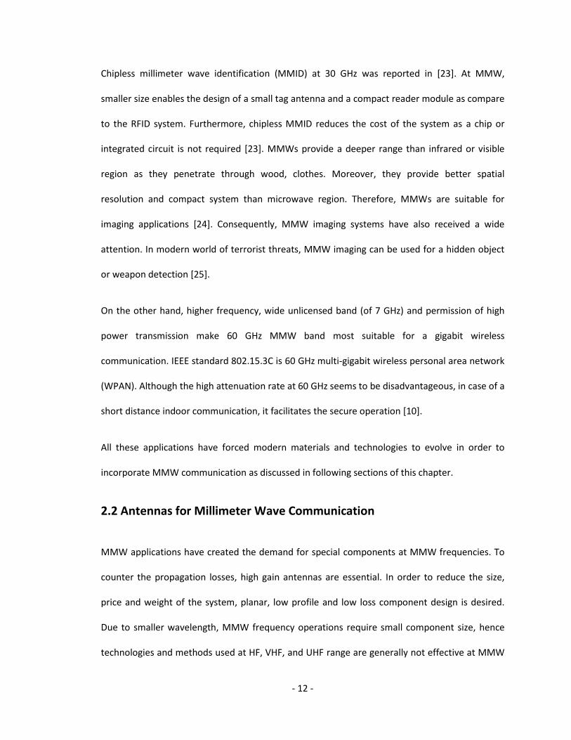
Figure 2.1 MMW horn antenna designs for (a) broadside radiation [28] and (b) endfire radiation [29]
Instead of a waveguide, other antenna structures are proposed to feed the horn shape for
MMW applications to obtain the reduction in a weight. A balanced fed patch is used to feed the
horn antenna for the design proposed in [30]. The multilayer pyramidal horn is designed using
the PCB process at MMWs in [28]. In this structure, substrate integrated waveguide with
transverse slots is used to feed the horn. This antenna structure could reach the gain of 12 dB.
Similar work is discussed in [21] where a hybrid (patch and horn) antenna is designed for a

- 14 -
broadside radiation. However, horn shape in a broadside direction results in the non-planar
structure.
Typically, the horn is a non-planar structure and used for an endfire radiation. Planar horns have
been attempted for MMW applications using a substrate integration technology. Flared
substrate integrated waveguide (SIW) can be used to construct the planar horn structure.
Coplanar waveguide (CPW) fed planar horn antenna is designed in [31] using the modern micro
fabrication procedure. In [32], waveguide feeding is used to make an H plane horn using PCB
process. Waveguide fed structure achieved in a gain of about 5-6 dB without loading due to
dielectric losses. In order to reduce the size of the structure, coaxial probe fed planar H plane
horn is designed in [33] based on half mode substrate integrated waveguide (HMSIW)
technology. It uses the principle of an electromagnetic field symmetry inside the waveguide.
However, the dielectric filled structure obstructs the propagation of electromagnetic waves
through the horn, resulting in reduction of gain. Therefore, attempts to design planar H-plane
horn using special Poly Tetra Fluoro Ethylene (PTFE) substrate [34] or air [35] as a substrate have
been made. Dielectric loading for a gain enhancement of H-plane horns are proposed in [36] and
[29]. Nevertheless, dielectric field planar horns exhibited gain from 5-8 dB with a compact size in
all these designs [29]-[36].
2.2.2 Lens Antennas
In order, to boost the gain of antenna elements, passive lenses are used ahead of moderate gain
antenna structures. At the very high frequency range, electromagnetic waves can be treated as
optical rays. At MMWs, the wavelength of the signal is very small, therefore lens antennas are
analyzed using a geometrical optics [10]. Term lens has been interchangeably used for dielectric
loading as well, in which case antenna substrate is extended in elliptical or random shape to
- 15 -
increase the gain of the structure [37]. The basic function of a dielectric lens is to transform a
spherical or cylindrical wavefront of an antenna element radiation into a planar wavefront to
achieve higher gain and narrow beamwidth [3]. When incident waves face the discontinuity
between the dielectric medium of lens and air, part of incident rays are transmitted and partially
they get refracted. In case of a convex lens, waves coming from a focal point bend towards the
normal of the surface. Many lens techniques, shapes and materials had been investigated in the
literature for millimeter wave antennas [10].
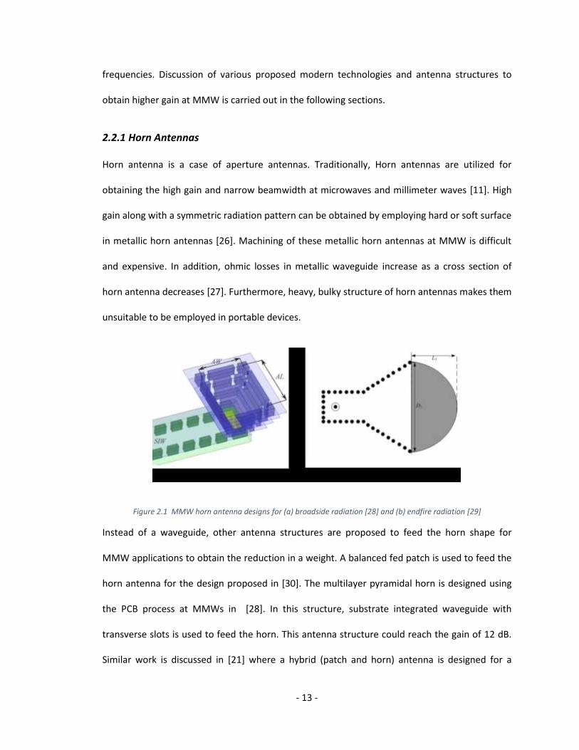
Figure 2.2 (a) half Maxwell fish-eye [38] and (b) Luneberg [39] lens antenna structures for MMW applications
Modified shaped cylindrical Luneberg lens antenna was presented for a front directed high gain.
This structure used a parallel plate technique. It has two parallel plates separated by air, in
which, the distance between the plates is varied to achieve the luneberg distribution in
refractive index of a lens [39]. Similarly, high gain is achieved using a mechanically steered lens
antenna for 60 GHz system. It has a circular horn followed by steerable hemispherical shaped
dielectric lens to achieve the beam control [40]. In addition, [38] proposed half Maxwell fish-eye
shaped antenna for a broadside radiation. It uses a multilayer lens structure with gradient-index.
In this structure, different shells with individual dielectric constants are used which allows
omnidirectional radiation pattern. Most part of ohmic losses in lens antennas are contributed by
the feed element, as a lens itself does not contribute in ohmic losses in a great deal. Although
- 16 -
these lens systems exhibit the high gain about 18-20 dB, use of lens makes the system bulky and
non-planar [39][40][38].
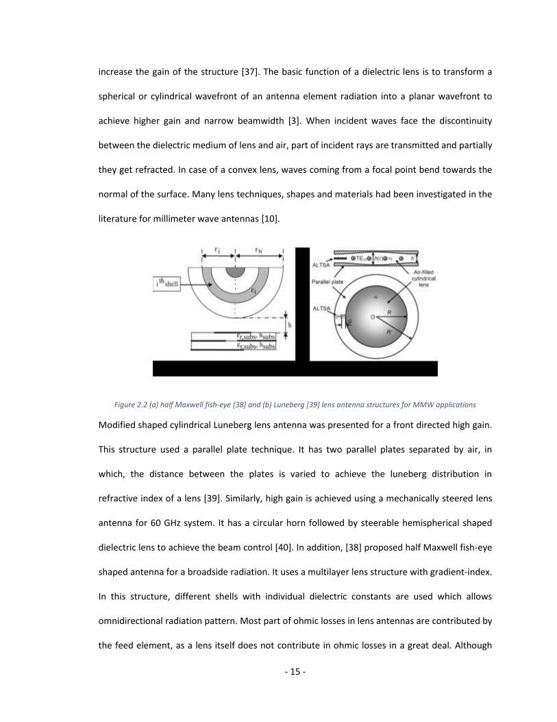
2.2.3 Dielectric Rod Antennas
Machining of metals is difficult, on the contrary, dielectrics are easy to machine and light weight.
Therefore, dielectric based antennas received the attention for MMW applications. Frequently,
the dielectric rod antenna had been proposed to achieve the endfire radiation. Dielectric rods
are easy to design and low cost antennas.
The radiation behavior of the dielectric rod antenna can be explained by the discontinuity
radiation concept [41] in which the antenna is regarded as an array composed of two effective
sources at the feed and the free end of the rod. Part of the power excited at the feed is
converted into guided-wave power, and is transformed into radiation power at the free (open)
end. The remaining power is converted into unguided-wave power radiating near the feed end.
Thus, the directivity of the dielectric rod antenna is characterized by the directivities generated
by these two effective sources. However, there is the problem of quantitatively computing the
radiation fields generated from the discontinuities at the feed and free ends [10].
Figure 2.3 Different shapes of dielectric rod antennas (a) step tapered [42] (b) flat top (c) H plane tapered (d) E and H Plane tapered dielectric rods
Although dielectric rods are typically used for endfire radiation, if dielectric rod is loaded with
metal strips, it can also be used for an omnidirectional radiation [43]. Linearly tapered [44] or

- 17 -
step tapered [42] dielectric rod antennas were extensively used as they provide an architecture
which is easily integrated with miniature waveguide systems [45]. It has also been observed that
a pointed dielectric rod has better performance than flat top dielectric rod antennas [44].
Variations of cylindrical dielectric rod antennas analyzed and utilized for array design in [46].
However, rods achieve moderate gain and offer the non-planar structures [42]-[46].
2.2.4 Slot Antennas
Figure 2.4 Slot antenna structures: (a) transverse slots on substrate integrated waveguide [47] and (b) slot director to enhance radiation pattern [48]
When a guided structure is loaded with perturbations, guiding wave propagating through
structure excites radiating leaky wave from the structure. Leaky wave antennas (LWAs) such as
slotted waveguide [49][50] had been in use for millimeter wave applications. When some type
of asymmetry is introduced in a cross section of a guided structure, it causes radiation by the
aperture. The degree of asymmetry will control the leakage rate and in turn the amplitude along
the line source [50]. These antenna structures use costly, heavy and bulky waveguide structures
as compared to the compact size of modern wireless application devices [47]. Furthermore,
higher ohmic losses are present due to the metallic structure.
Planar substrate integrated waveguide slot antenna for a broadside radiation had been
proposed in [47]. In this design, a periodic set of transverse slots are etched on a planar
substrate integrated waveguide to obtain the broadside radiation. In this design spacing

- 18 -
between the consecutive slots decides the maxima direction of the radiation pattern. However,
an ohmic loss analysis of this design shows that the conductor loss of slotted SIW is larger than
the conductor loss of a corresponding closed rectangular waveguide. This is due to the fact that
the current must bend around the slots, increasing the current density surrounding the slots,
resulting in increased conductor loss [47].
Similar to yagi-uda antenna structure, directors ahead of slot structure are proposed in [48] to
obtain the high gain in a broadside direction. It uses single layer 1, 3 or 5 slot directors to
enhance the gain. However, introducing the directors and reflectors in either side of principle
slot structure results in a bigger antenna structure.
2.2.5 Dielectric Resonator Antennas (DRA)
Figure 2.5 (a) Pentagonal [51] and (b) cylindrical [52] dielectric resonator antenna structures
Dielectric resonator antennas are used for MMW communication as broadside radiating
elements. They are superior in terms of low ohmic losses, low dissipation. No surface waves in
the DRA structures make them suitable for array designing where no mutual coupling between
elements makes designing easier. Pentagon shaped aperture coupled dielectric resonator
antenna is presented in [51]. It uses dielectric pentagon over an aperture to focus the radiation
in broadside direction. In this design, aperture coupling from microstrip line is used to excite the
dielectric resonator. One of the attraction of DRAs is their shape, it can assume cylindrical [52],
- 19 -
cubical [53], pentagonal [51] shape according to the available size without affecting the
radiation pattern characteristics. However, if the height of dielectric resonator is significant, it
results in a non-planar, high profile antenna structure.
2.2.6 Microstrip Antennas
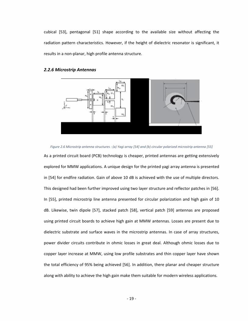
Figure 2.6 Microstrip antenna structures : (a) Yagi array [54] and (b) circular polarized microstrip antenna [55]
As a printed circuit board (PCB) technology is cheaper, printed antennas are getting extensively
explored for MMW applications. A unique design for the printed yagi array antenna is presented
in [54] for endfire radiation. Gain of above 10 dB is achieved with the use of multiple directors.
This designed had been further improved using two layer structure and reflector patches in [56].
In [55], printed microstrip line antenna presented for circular polarization and high gain of 10
dB. Likewise, twin dipole [57], stacked patch [58], vertical patch [59] antennas are proposed
using printed circuit boards to achieve high gain at MMW antennas. Losses are present due to
dielectric substrate and surface waves in the microstrip antennas. In case of array structures,
power divider circuits contribute in ohmic losses in great deal. Although ohmic losses due to
copper layer increase at MMW, using low profile substrates and thin copper layer have shown
the total efficiency of 95% being achieved [56]. In addition, there planar and cheaper structure
along with ability to achieve the high gain make them suitable for modern wireless applications.
- 20 -
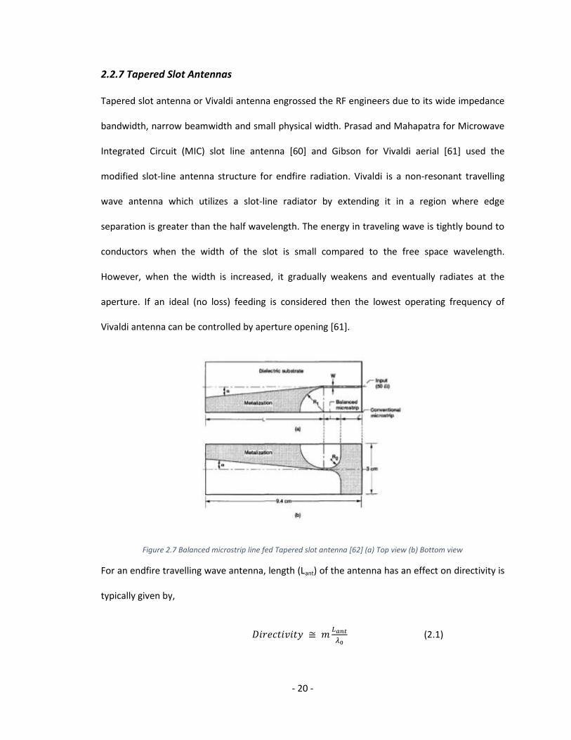
2.2.7 Tapered Slot Antennas
Tapered slot antenna or Vivaldi antenna engrossed the RF engineers due to its wide impedance
bandwidth, narrow beamwidth and small physical width. Prasad and Mahapatra for Microwave
Integrated Circuit (MIC) slot line antenna [60] and Gibson for Vivaldi aerial [61] used the
modified slot-line antenna structure for endfire radiation. Vivaldi is a non-resonant travelling
wave antenna which utilizes a slot-line radiator by extending it in a region where edge
separation is greater than the half wavelength. The energy in traveling wave is tightly bound to
conductors when the width of the slot is small compared to the free space wavelength.
However, when the width is increased, it gradually weakens and eventually radiates at the
aperture. If an ideal (no loss) feeding is considered then the lowest operating frequency of
Vivaldi antenna can be controlled by aperture opening [61].
Figure 2.7 Balanced microstrip line fed Tapered slot antenna [62] (a) Top view (b) Bottom view
For an endfire travelling wave antenna, length (Lant) of the antenna has an effect on directivity is
typically given by,
(2.1)

- 21 -
where, λ0 is the free space wavelength. If the length of the antenna is in the range of 3λ0 < L <
8λ0, then m = 10. However, the value of m decreases for antennas longer than 8λ0 [63].
Figure 2.8 Electric field line orientation for (a) unbalanced microstrip line (b) Balanced microstrip line (c) antipodal tapered slot
Numerous ways had been proposed to excite the tapered slot to a design planar structure.
Microstrip line is an unbalanced structure due to its ground plane, whereas tapered slot antenna
having two conductors separated by a slot, is symmetric or balanced structure. In [62], balanced
microstrip is presented to serve the purpose of a balun. Balun (also called as Balance-
Unbalance) is a transition between balance and unbalanced transmission line which also serves
the purpose of impedance matching between the two lines [11]. Ground plane of an unbalanced
microstrip line is gradually decreased, as shown in Fig. 2.7, to match the width of microstrip line
(W50). Gradual taper facilitates impedance matching between conventional and balanced
microstrip. Non-planar tapered slot antenna was designed by flaring the balanced microstrip
conductors in the opposite direction. Fig. 2.8 shows the electric field orientation in conventional
microstrip, balanced microstrip and non-planar tapered slot antenna. Balanced microstrip has
concentrated electric field lines as compared to the unbalanced microstrip line, whereas electric
field lines rotate along the axis of the antenna when slot width is increased gradually [62]. Non-
planar tapered slot antenna is also called as Antipodal Tapered Slot Antenna (ALTSA).

- 22 -
Figure 2.9 SIW fed ALTSA [64]
As substrate integrated waveguide (SIW) is one of the balanced structure having similar electric
field orientation as balanced microstrip line, SIW was used for feeding ALTSA. SIW prevails over
the conventional microstrip line regarding an insertion loss performance at microwave and
MMW frequencies. The typical impedance of ALTSA is approximately 160Ω, whereas impedance
of the SIW is limited by the height of substrate. Therefore, tapered slot is backwardly extended
to prevent this matching. Low input impedance is obtained by crossing the metallic covers of
tapered slot for short distance [64]. Although SIW feed for ALTSA is also proposed in [65], it uses
CPW feeding, which is unable to obtain 50Ω input impedance. In [65], minimum input
impedance of 74Ω is achieved.
Tapered slot antennas are most suitable for MMW endfire radiation application due to their
planar structure, low losses and high gain capability.
2.2.8 Comparison of various Millimeter Wave Antennas
Gain capability and size of structure are few of the important characteristics to achieve the
objective of this thesis. Therefore, antenna structures discussed in literature are compared in
Table (2.1).

- 23 -
Table 2.1 Gain and size comparison for Millimeter wave Antennas
Antenna Structure Radiation Gain capability Planar structure
Horn Antennas Endfire Moderate Planar/Non-planar
Broadside Moderate Non-Planar
Lens Antenna Endfire High Non-Planar
Dielectric Rod Endfire High Non-Planar
Slot Antenna Broadside Moderate Planar
Dielectric Resonator Antenna Broadside Moderate Non-Planar
Microstrip Antenna Broadside Moderate Planar
Endfire Moderate Planar
Tapered Slot Antenna Endfire High Planar
In a summary, highly efficient dielectric resonator antennas proposed for the broadside
radiation. However, they achieve only moderate gain and more importantly offer non-planar
structures. Although lens antennas have exhibited the high gain, they have non-planar structure
as well. As in planar structures, slot apertures and printed antennas are proposed. However, slot
apertures suffer from higher ohmic losses. In case of endfire radiation, although horn antennas
are proposed in planar structure, they offer relatively lower gain for the endfire case. Even
dielectric rod antennas which are proposed for endfire radiation have non-planar structures.
2.3 Numerical Techniques for Full wave analysis
Radiation fields and scattering matrix of an antenna can be obtained by solving the Maxwell
equations satisfying the boundary conditions for the structure. At the core of any
electromagnetic problem are the Maxwell’s equations. Solution of Maxwell’s equation without

- 24 -
any physical approximation is called as Full wave analysis. However, the actual solution of
Maxwell’s equations is very complex and computational electromagnetics is used to solve the
Maxwell’s equations using computer programs. There are numerous CAD tools available for full
wave analysis of electromagnetic structures. Although these tools do not consider any physical
approximation, they solve the equations using different numerical techniques which assume
certain numerical approximations. Use of any of the numerical methods involves three steps
[66]:
1. Preprocessing, to derive the coefficients in the algebraic equations
2. Solutions of the algebraic equations
3. Interpretation of results
Few numerical techniques used for electromagnetics are [66]:
1. Method of Moment (MoM)
2. Finite Difference Time Domain (FDTD)
3. Finite Element Method (FEM)
4. Finite Integration Technique (FIT)
5. Fast Multipole Method (FMM)
6. Transmission Line Matrix (TLM)
7. Uniform Theory of Diffraction (UTD)
Each technique is suitable for particular types of problems. There is not one sufficient and
effective technique for all types of electromagnetics problems. Method of moment uses integral
equations and it is suitable for the problem which consist of conductive surfaces only,
homogeneous dielectrics only or specific conductor-dielectric shapes only. It does not handle
electromagnetically penetrable materials [67]. In FDTD method values of the next time step are

- 25 -
calculated based on values at current and previous time steps. Therefore, this method is not
unconditionally stable [67]. FDTD method is efficient for problems with non-isotropic materials.
It requires grid with size of smallest dimension in structure, it may run into issues of large
computational requirement [68]. In TLM, each node is connected to its adjacent node via a pair
of orthogonally connected virtual transmission lines. However, similar to FDTD it has problem of
large complexity when huge structures are to be analyzed [68]. UTD approximates
electromagnetic wave as the light ray. Therefore, it is accurate only for high frequency
calculations [68]. Integral solver FMM uses much lesser points to solve the equation. It needs
smaller storage memory, however, it is suitable only for plane wave excitations problems [69].
Full wave analysis of antenna structures presented in this thesis is carried out using CST
Microwave studio, which uses the Finite Integration Technique (FIT) and HFSS which uses the
Finite Element Method (FEM). These numerical techniques are discussed in following sections.
2.3.1 Finite Element Method
The basic concept of the finite element method is that although the behaviour of the function
may be complex when viewed over a large region, a simple approximation may suffice for a
small subregion. The total structure is subdivided into smaller finite elements. In three
dimensional structures tetrahedron, hexahedron, prism, pyramid shapes are used as finite
elements because they can cover the complex structures as well. Fields are calculated at nodes
and approximated by interpolation on each element using differential expressions. The field
representation is continuous at the edges where elements overlap. The equations to be solved
are in terms of an integral type functional such as energy. The total functional is the sum of the
integral over each element [66].

- 26 -
Figure 2.10 Subdivision of a region using finite elements
The discretization step can be easy or complex depending upon the curvature and size of the
structure. Fig. 2.10 shows a simple rectangle has been subdivided using square elements,
however irregular triangles are used to divide the irregular and slightly complex shape. For any
three dimensional electromagnetic structure, three independent spatial co-ordinates are
required for the discretization of the region. Tetrahedron shaped finite elements are used in
HFSS CAD tool as they model even the complex structures accurately.
An approximate functional (φn) is calculated for element n and quantity is interrelated in all N
elements such that it is continuous at boundaries. The approximate solution for the whole
region is then sum of all element potentials as given by (2.2).
( ) ∑ ( ) (2.2)
Figure 2.11 Irregular triangular element with three nodes
Functional is generally a polynomial approximation such as (2.3) for triangular element.
However, higher order interpolation is required in more complex examples.

- 27 -
( ) (2.3)
Functional values for vertices of irregular triangular element as in Fig. 2.11 can be given by
matrix notation,
[
] [ ] [
] (2.4)
The determinant of the coefficients is given by the following equation where A is the area of a
triangle.
|
| (2.5)
When equations are solved for a,b and c. We get,
( ) ∑ ( ) (2.6)
Which gives,
( )
[( ) ( ) ( ) ] (2.7)
Similar function is obtained for second and third row. The are interpolation functions in the
sense that,
( ) *
(2.8)
In case of capacitance example, gradient of ( ) can be used to find the energy in the
element. Calculation for two dimensional structure established portrays the complexity to be
faced with a huge three dimensional structures.

- 28 -
Error sources in finite element method are discretization, formulation and numerical. Using less
number of elements might speed up the process, however it will result in inaccurate results.
Shaper of the element can contribute in the error of calculation. Therefore, the proper
formulation of specific problem is important. Numerical errors are concerned with the CAD tool
program and their ability to handle larger numbers.
2.3.2 Finite Integration Technique
The key concept for the finite integration technique is to use in discretization the integral rather
than a differential form of Maxwell’s equations. There are two primary aspects of FIT which
makes it popular. Firstly, it is not only applicable for frequency domain, but also for time domain
calculation. Therefore, huge and complex structures can be solved using FIT. In addition, it is
applicable to a variety of discretization types [70].
Prior to start the electromagnetic calculation, the structure is discretized using mesh.
Tetrahedron, staircase-hexahedron can be used for it as shown in Fig. 2.12. The hexahedron
type mesh is more suitable for time domain calculation, on the other hand tetrahedron type
mesh is more suitable for frequency domain calculation and covers the surface with fine details.
If electromagnetic example is considered then Maxwell equations are written for the individual
mesh element. For hexahedron element in Fig. 2.12 (c),
(2.9)
When all electric and magnetic quantities are considered, Maxwell equation can be written in
matrix form.
(2.10)
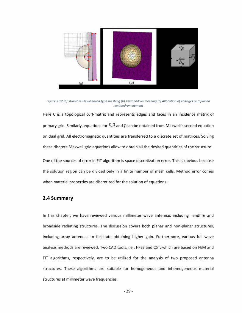
- 29 -
Figure 2.12 (a) Staircase-Hexahedron type meshing (b) Tetrahedron meshing (c) Allocation of voltages and flux on hexahedron element
Here C is a topological curl-matrix and represents edges and faces in an incidence matrix of
primary grid. Similarly, equations for and can be obtained from Maxwell’s second equation
on dual grid. All electromagnetic quantities are transferred to a discrete set of matrices. Solving
these discrete Maxwell grid equations allow to obtain all the desired quantities of the structure.
One of the sources of error in FIT algorithm is space discretization error. This is obvious because
the solution region can be divided only in a finite number of mesh cells. Method error comes
when material properties are discretized for the solution of equations.
2.4 Summary
In this chapter, we have reviewed various millimeter wave antennas including endfire and
broadside radiating structures. The discussion covers both planar and non-planar structures,
including array antennas to facilitate obtaining higher gain. Furthermore, various full wave
analysis methods are reviewed. Two CAD tools, i.e., HFSS and CST, which are based on FEM and
FIT algorithms, respectively, are to be utilized for the analysis of two proposed antenna
structures. These algorithms are suitable for homogeneous and inhomogeneous material
structures at millimeter wave frequencies.
- 30 -
Chapter 3
Four element aperture coupled patch antenna is presented for Ka-band millimeter wave
communication. Section 3.1 introduces microstrip antenna and working of the antenna
structure. Section 3.2 elaborates the design methodology for the proposed structure. Section
3.3 shows proposed structure and design parameters. Section 3.4 follows with the study about
the effects of various parameters on antenna performance. In the end, section 3.5 exhibits the
designed prototype with simulation and measured results.
3.1 Microstrip Antenna
3.1.1 Introduction
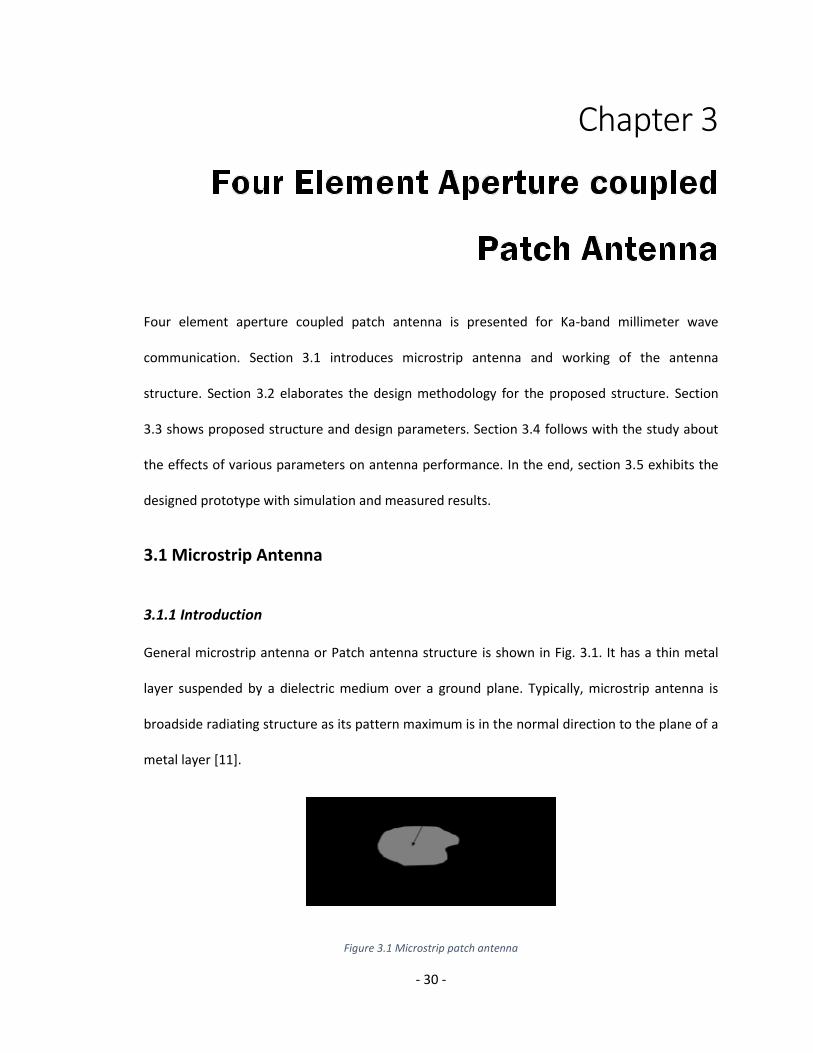
General microstrip antenna or Patch antenna structure is shown in Fig. 3.1. It has a thin metal
layer suspended by a dielectric medium over a ground plane. Typically, microstrip antenna is
broadside radiating structure as its pattern maximum is in the normal direction to the plane of a
metal layer [11].
Figure 3.1 Microstrip patch antenna
- 31 -
Linear as well as circular polarization can be achieved by patch antennas. Following
characteristics of patch antennas mark them favorable for modern high frequency applications
[11]:
1. Planar structure
2. Low profile
3. Compatible with printed circuit technology
4. Easy to use in array structures
3.1.2 Feeding Techniques
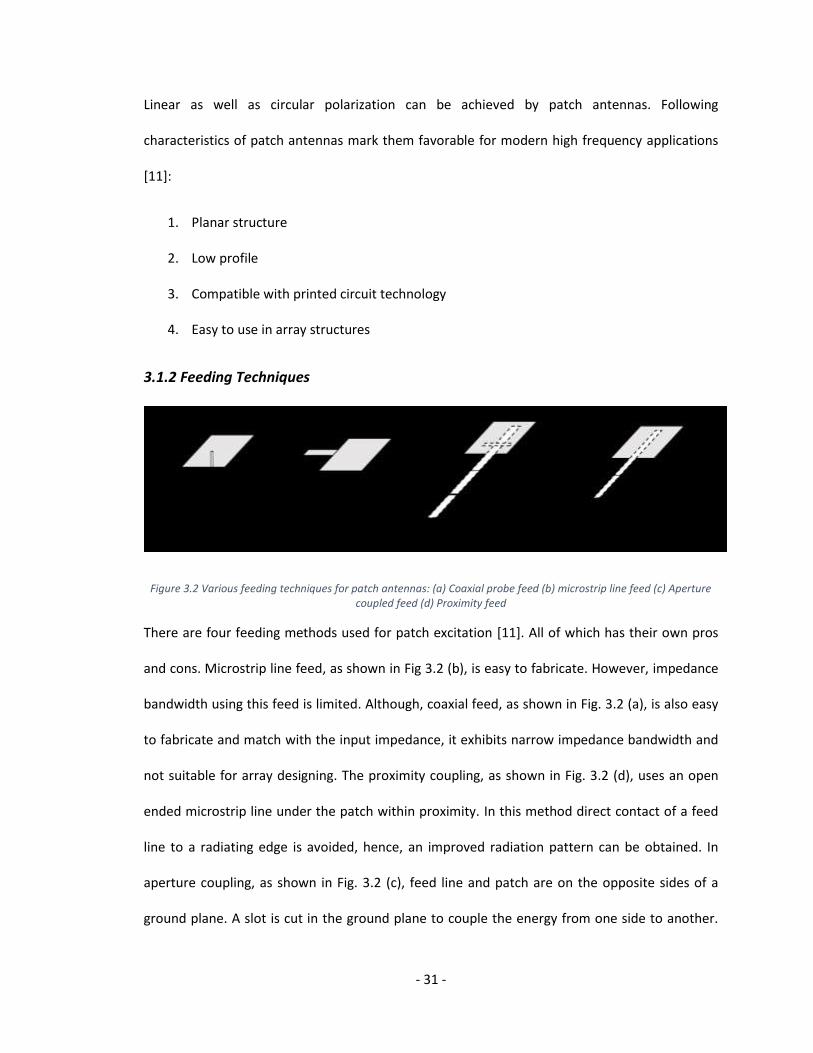
Figure 3.2 Various feeding techniques for patch antennas: (a) Coaxial probe feed (b) microstrip line feed (c) Aperture coupled feed (d) Proximity feed
There are four feeding methods used for patch excitation [11]. All of which has their own pros
and cons. Microstrip line feed, as shown in Fig 3.2 (b), is easy to fabricate. However, impedance
bandwidth using this feed is limited. Although, coaxial feed, as shown in Fig. 3.2 (a), is also easy
to fabricate and match with the input impedance, it exhibits narrow impedance bandwidth and
not suitable for array designing. The proximity coupling, as shown in Fig. 3.2 (d), uses an open
ended microstrip line under the patch within proximity. In this method direct contact of a feed
line to a radiating edge is avoided, hence, an improved radiation pattern can be obtained. In
aperture coupling, as shown in Fig. 3.2 (c), feed line and patch are on the opposite sides of a
ground plane. A slot is cut in the ground plane to couple the energy from one side to another.
- 32 -
Although this method is difficult to fabricate, it provides stronger coupling than proximity
feeding. Also, aperture coupling allows high permittivity dielectric material to be used for feed
design without compromising low permittivity material in radiation side. Improvement in the
impedance bandwidth and compatibility with array design make it favorable for higher gain,
wideband applications.
3.2 Design of Four Element Patch Radiator
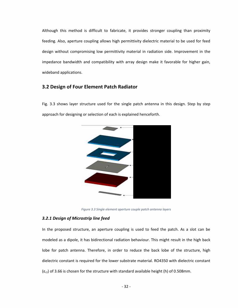
Fig. 3.3 shows layer structure used for the single patch antenna in this design. Step by step
approach for designing or selection of each is explained henceforth.
Figure 3.3 Single element aperture couple patch antenna layers
3.2.1 Design of Microstrip line feed
In the proposed structure, an aperture coupling is used to feed the patch. As a slot can be
modeled as a dipole, it has bidirectional radiation behaviour. This might result in the high back
lobe for patch antenna. Therefore, in order to reduce the back lobe of the structure, high
dielectric constant is required for the lower substrate material. RO4350 with dielectric constant
(εr2) of 3.66 is chosen for the structure with standard available height (h) of 0.508mm.
- 33 -
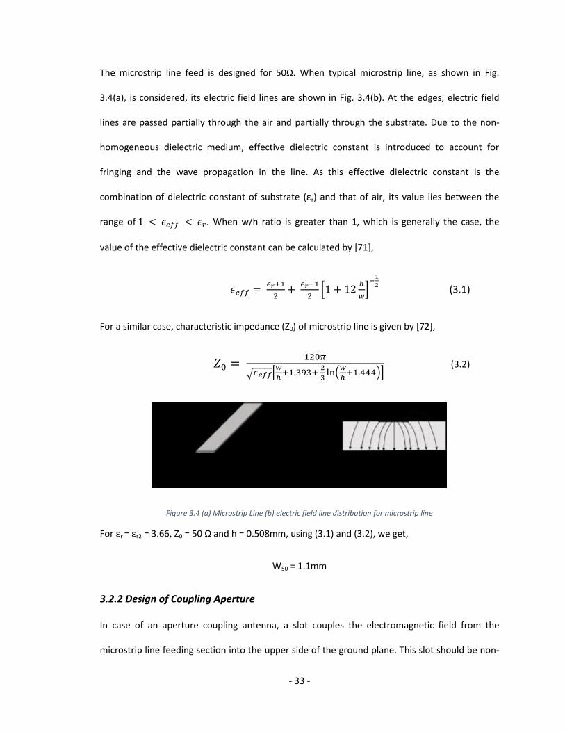
The microstrip line feed is designed for 50Ω. When typical microstrip line, as shown in Fig.
3.4(a), is considered, its electric field lines are shown in Fig. 3.4(b). At the edges, electric field
lines are passed partially through the air and partially through the substrate. Due to the non-
homogeneous dielectric medium, effective dielectric constant is introduced to account for
fringing and the wave propagation in the line. As this effective dielectric constant is the
combination of dielectric constant of substrate (εr) and that of air, its value lies between the
range of . When w/h ratio is greater than 1, which is generally the case, the
value of the effective dielectric constant can be calculated by [71],
*
+
(3.1)
For a similar case, characteristic impedance (Z0) of microstrip line is given by [72],
√ *
(
)+
(3.2)
Figure 3.4 (a) Microstrip Line (b) electric field line distribution for microstrip line
For εr = εr2 = 3.66, Z0 = 50 Ω and h = 0.508mm, using (3.1) and (3.2), we get,
W50 = 1.1mm
3.2.2 Design of Coupling Aperture
In case of an aperture coupling antenna, a slot couples the electromagnetic field from the
microstrip line feeding section into the upper side of the ground plane. This slot should be non-
- 34 -
resonant as resonant slot increases the back radiation of the antenna [73]. Length of slot is
chosen such that close matching is achieved at the center frequency. It is chosen to fix the
resistive part as shown in Fig. 3.6(a). For open transmission line, as shown in Fig. 3.5, voltage is
maximum and current is zero at the open end. The distance between consecutive maxima and
minima is half a wavelength [74]. First current maximum from open ended line is a quarter
wavelength away from the end.
Figure 3.5 Open ended transmission line and current distribution over the line
Figure 3.6 Effect on impedance matching of (a) slot length and (b) open stub length
For 28 GHz centre frequency, free space wavelength is
and guided
wavelength is
√ . Therefore, theoretically aperture should be positioned

- 35 -
1.4mm away from the open end of the microstrip feed line. However, the length of this open
circuit stub has an effect on reactive part of an input impedance of an antenna as shown in Fig.
3.6(b). Therefore, the length of the open stub is chosen to be 1.3mm.
3.2.3 Design of Patch Element
An impedance bandwidth is proportional to the volume of the structure [11]. In case of
rectangular patch it can be given by (3.4). Although the length and the width cannot be changed
as it will affect the resonance frequency, an impedance bandwidth can be improved by
increasing the height of the structure. Nevertheless, if (3.3) is rewritten using electrical
dimensions, then (3.4) is relates the impedance bandwidth to the relative permittivity of the
substrate. Therefore, the impedance bandwidth of the patch is inversely proportional to the
square root of the relative permittivity of the substrate.
(3.3)
√
√ √
√ (3.4)
If the air gap of thickness ∆ is introduced below the substrate of height ‘h’ and relative
permittivity εr then equivalent relative permittivity can be given by [73],
( )
( ) (3.5)
Therefore, air gap of 0.254mm is introduced with substrate RO6002 height (h) of 0.127mm.
RO6002 has relative permittivity of 2.94. Using (3.5), equivalent a relative permittivity is 1.15 is
obtained. Due to the fringing effect, a patch looks larger than its physical dimensions, as
illustrated in Fig. 3.7. Effective length (Leff) is larger by ∆L from both sides.
- 36 -
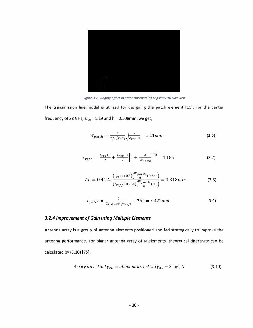
Figure 3.7 Fringing effect in patch antenna (a) Top view (b) side view
The transmission line model is utilized for designing the patch element [11]. For the center
frequency of 28 GHz, εreq = 1.19 and h = 0.508mm, we get,
√ √
(3.6)
[
]
(3.7)
( )(
)
( )(
)
(3.8)
√ √ (3.9)
3.2.4 Improvement of Gain using Multiple Elements
Antenna array is a group of antenna elements positioned and fed strategically to improve the
antenna performance. For planar antenna array of N elements, theoretical directivity can be
calculated by (3.10) [75].
(3.10)

- 37 -
Figure 3.8 Array factor for four elements uniformly fed equidistant array
Fig. 3.8 shows, an array factor for uniformly excited equally spaced four elements. If the
distance between successive elements is greater than the critical value, second major lobe will
appear in the radiation pattern of an array. This undesirable major lobe is called as a grating
lobe. As shown in Fig. 3.8, a grating lobe can be avoided by keeping the value of ψ less than
3π/2. Variable ψ is dependent on the distance between elements which gives an upper bound
for distance between elements [75].
(3.11)
The behaviour of a current on transmission line is already discussed in section 3.2.2. From Fig.
3.5, a maxima reoccurs after every Nλ/2 distance from the first maxima. Therefore, spacing
between aperture slots is kept a guided wavelength. It also satisfies the (3.11).
√ (3.12)
It completes the theoretical design procedure for patch element.
3.3 Proposed Structure and Design Parameters
Fig. 3.9 shows the proposed antenna structure of four element patch antenna. Dimensions of
the structure are 31 x 10 x 0.94 mm3. Table (3.1) gives the optimized dimensions of design

- 38 -
parameters. Table (3.2) exhibits the details of dielectric materials used for the structure. Results
are discussed in the following sections.
Figure 3.9 Proposed four element patch antenna structure (a) in 3D and (b) in layer separation view
Table 3.1 Design parameters and their dimensions for proposed structure
Design Parameter Dimension (millimeter)
Length of patch element (LPatch) 3.2
Width of patch element (WPatch) 5.5
Length of substrate (L) 31
Width of substrate (W) 10
Length of air-gap cavity (LG) 4
Width of air-gap cavity (WG) 5.5
Height of air-gap cavity (HG) 0.254
Height of upper substrate (HU) 0.127
Distance between elements (Spacing) 6.3
Length of aperture(SL) 5.4
Width of aperture(SW) 0.21
Length of open stub (QTW) 1.29
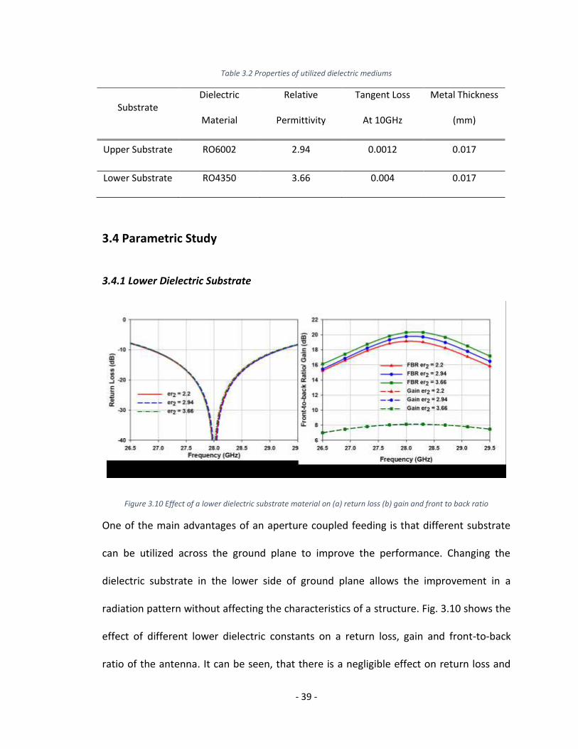
- 39 -
Table 3.2 Properties of utilized dielectric mediums
Substrate Dielectric
Material
Relative
Permittivity
Tangent Loss
At 10GHz
Metal Thickness
(mm)
Upper Substrate RO6002 2.94 0.0012 0.017
Lower Substrate RO4350 3.66 0.004 0.017
3.4 Parametric Study
3.4.1 Lower Dielectric Substrate
Figure 3.10 Effect of a lower dielectric substrate material on (a) return loss (b) gain and front to back ratio
One of the main advantages of an aperture coupled feeding is that different substrate
can be utilized across the ground plane to improve the performance. Changing the
dielectric substrate in the lower side of ground plane allows the improvement in a
radiation pattern without affecting the characteristics of a structure. Fig. 3.10 shows the
effect of different lower dielectric constants on a return loss, gain and front-to-back
ratio of the antenna. It can be seen, that there is a negligible effect on return loss and
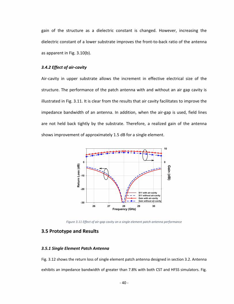
- 40 -
gain of the structure as a dielectric constant is changed. However, increasing the
dielectric constant of a lower substrate improves the front-to-back ratio of the antenna
as apparent in Fig. 3.10(b).
3.4.2 Effect of air-cavity
Air-cavity in upper substrate allows the increment in effective electrical size of the
structure. The performance of the patch antenna with and without an air gap cavity is
illustrated in Fig. 3.11. It is clear from the results that air cavity facilitates to improve the
impedance bandwidth of an antenna. In addition, when the air-gap is used, field lines
are not held back tightly by the substrate. Therefore, a realized gain of the antenna
shows improvement of approximately 1.5 dB for a single element.
Figure 3.11 Effect of air-gap cavity on a single element patch antenna performance
3.5 Prototype and Results
3.5.1 Single Element Patch Antenna
Fig. 3.12 shows the return loss of single element patch antenna designed in section 3.2. Antenna
exhibits an impedance bandwidth of greater than 7.8% with both CST and HFSS simulators. Fig.
Frequency (GHz)26 27 28 29 30
Retu
rn L
oss (
dB
)
-30
-20
-10
0
10
Gain
(dB
)
-30
-20
-10
0
10
S11 with air-cavity
S11 without air-cavity
Gain with air-cavity
Gain without air-cavity
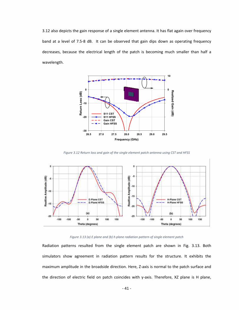
- 41 -
3.12 also depicts the gain response of a single element antenna. It has flat again over frequency
band at a level of 7.5-8 dB. It can be observed that gain dips down as operating frequency
decreases, because the electrical length of the patch is becoming much smaller than half a
wavelength.
Figure 3.12 Return loss and gain of the single element patch antenna using CST and HFSS
Figure 3.13 (a) E plane and (b) h plane radiation pattern of single element patch
Radiation patterns resulted from the single element patch are shown in Fig. 3.13. Both
simulators show agreement in radiation pattern results for the structure. It exhibits the
maximum amplitude in the broadside direction. Here, Z-axis is normal to the patch surface and
the direction of electric field on patch coincides with y-axis. Therefore, XZ plane is H plane,
Frequency (GHz)
26.5 27.0 27.5 28.0 28.5 29.0 29.5
Re
turn
Lo
ss
(d
B)
-30
-20
-10
0
10
Re
aliz
ed
Ga
in (d
B)
-30
-20
-10
0
10
S11 CST
S11 HFSS
Gain CST
Gain HFSS
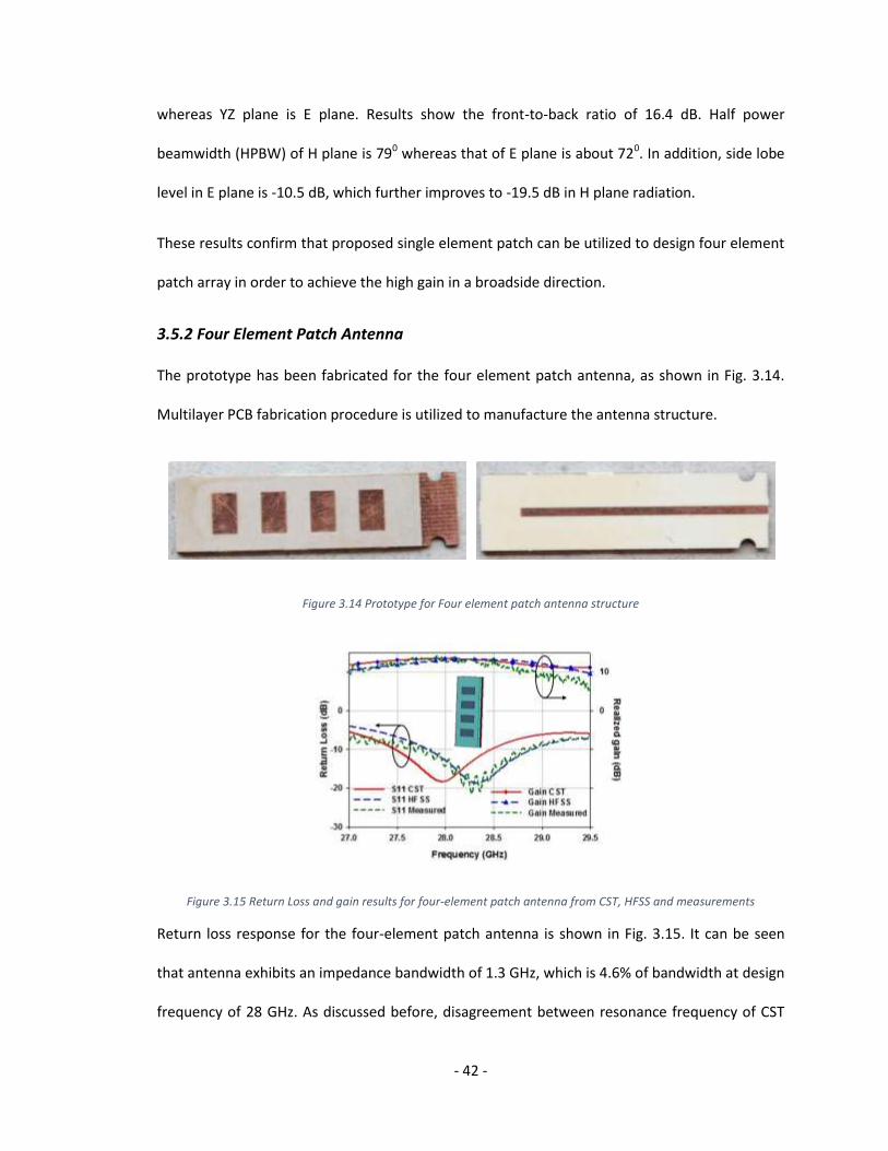
- 42 -
whereas YZ plane is E plane. Results show the front-to-back ratio of 16.4 dB. Half power
beamwidth (HPBW) of H plane is 790 whereas that of E plane is about 720. In addition, side lobe
level in E plane is -10.5 dB, which further improves to -19.5 dB in H plane radiation.
These results confirm that proposed single element patch can be utilized to design four element
patch array in order to achieve the high gain in a broadside direction.
3.5.2 Four Element Patch Antenna
The prototype has been fabricated for the four element patch antenna, as shown in Fig. 3.14.
Multilayer PCB fabrication procedure is utilized to manufacture the antenna structure.
Figure 3.14 Prototype for Four element patch antenna structure
Figure 3.15 Return Loss and gain results for four-element patch antenna from CST, HFSS and measurements
Return loss response for the four-element patch antenna is shown in Fig. 3.15. It can be seen
that antenna exhibits an impedance bandwidth of 1.3 GHz, which is 4.6% of bandwidth at design
frequency of 28 GHz. As discussed before, disagreement between resonance frequency of CST
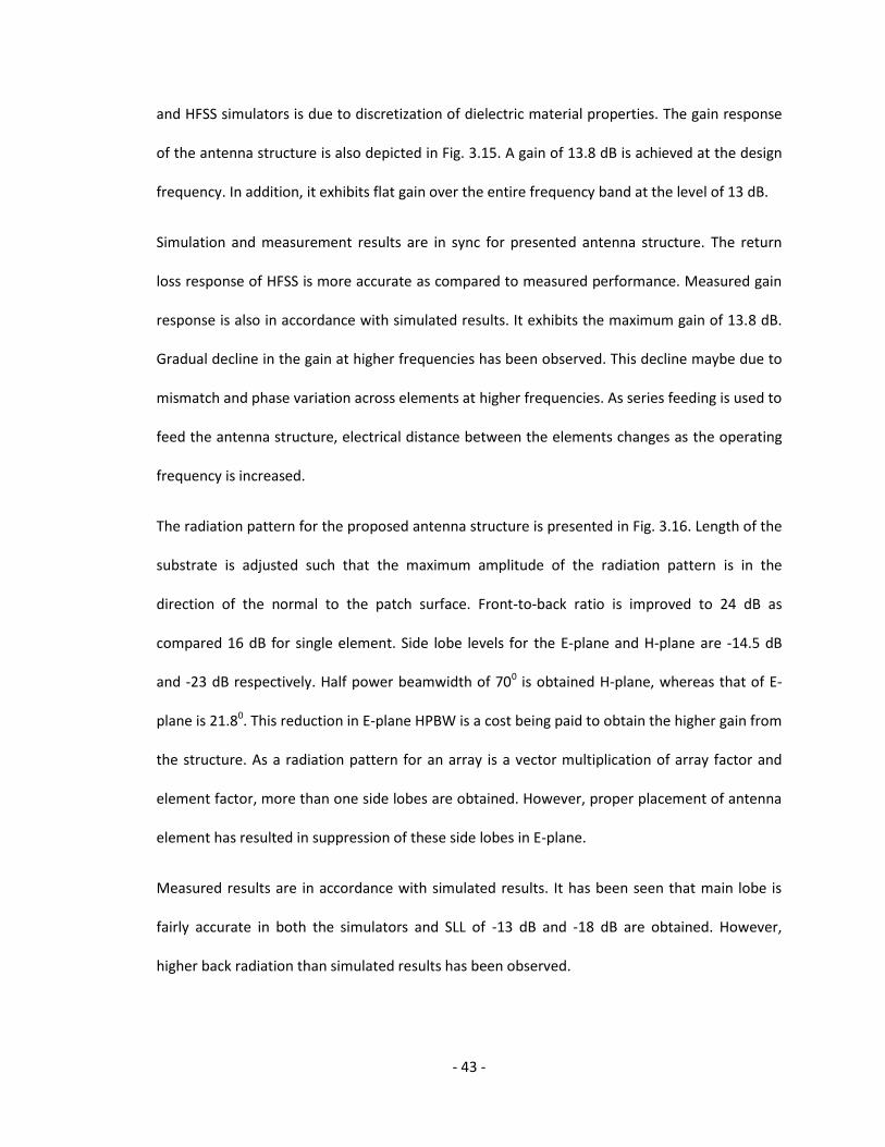
- 43 -
and HFSS simulators is due to discretization of dielectric material properties. The gain response
of the antenna structure is also depicted in Fig. 3.15. A gain of 13.8 dB is achieved at the design
frequency. In addition, it exhibits flat gain over the entire frequency band at the level of 13 dB.
Simulation and measurement results are in sync for presented antenna structure. The return
loss response of HFSS is more accurate as compared to measured performance. Measured gain
response is also in accordance with simulated results. It exhibits the maximum gain of 13.8 dB.
Gradual decline in the gain at higher frequencies has been observed. This decline maybe due to
mismatch and phase variation across elements at higher frequencies. As series feeding is used to
feed the antenna structure, electrical distance between the elements changes as the operating
frequency is increased.
The radiation pattern for the proposed antenna structure is presented in Fig. 3.16. Length of the
substrate is adjusted such that the maximum amplitude of the radiation pattern is in the
direction of the normal to the patch surface. Front-to-back ratio is improved to 24 dB as
compared 16 dB for single element. Side lobe levels for the E-plane and H-plane are -14.5 dB
and -23 dB respectively. Half power beamwidth of 700 is obtained H-plane, whereas that of E-
plane is 21.80. This reduction in E-plane HPBW is a cost being paid to obtain the higher gain from
the structure. As a radiation pattern for an array is a vector multiplication of array factor and
element factor, more than one side lobes are obtained. However, proper placement of antenna
element has resulted in suppression of these side lobes in E-plane.
Measured results are in accordance with simulated results. It has been seen that main lobe is
fairly accurate in both the simulators and SLL of -13 dB and -18 dB are obtained. However,
higher back radiation than simulated results has been observed.
- 44 -
Figure 3.16 (a) E plane and (b) H plane radiation pattern for proposed structure
Fig. 3.17 illustrates the effect of changing the operating frequency on the radiation pattern of
the proposed antenna structure. No significant effect was observed in H plane radiation at lower
and higher end frequencies. However, as clear from Fig. 3.17 (a), peak of the radiation pattern
shifts towards the forward direction as the operating frequency is increased. In addition, side
lobe level in the backward direction deteriorates with an increase in the frequency.
Figure 3.17 (a) E plane and (b) H plane radiation patterns of proposed antenna structure at 27.3, 28 and 28.7 GHz
Fig. 3.18 shows the efficiency of the antenna structure. Dielectric material, metallic patch as well
as microstrip line contribute to ohmic losses in the proposed antenna structure. However, total
efficiency above 85-90% is observed in the operating frequency band.
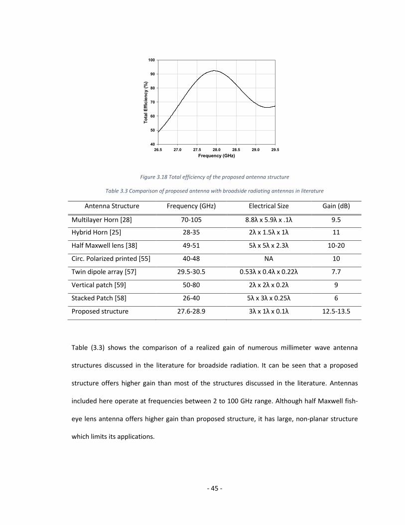
- 45 -
Frequency (GHz)
26.5 27.0 27.5 28.0 28.5 29.0 29.5T
ota
l E
ffic
ien
cy (
%)
40
50
60
70
80
90
100
Figure 3.18 Total efficiency of the proposed antenna structure
Table 3.3 Comparison of proposed antenna with broadside radiating antennas in literature
Antenna Structure Frequency (GHz) Electrical Size Gain (dB)
Multilayer Horn [28] 70-105 8.8λ x 5.9λ x .1λ 9.5
Hybrid Horn [25] 28-35 2λ x 1.5λ x 1λ 11
Half Maxwell lens [38] 49-51 5λ x 5λ x 2.3λ 10-20
Circ. Polarized printed [55] 40-48 NA 10
Twin dipole array [57] 29.5-30.5 0.53λ x 0.4λ x 0.22λ 7.7
Vertical patch [59] 50-80 2λ x 2λ x 0.2λ 9
Stacked Patch [58] 26-40 5λ x 3λ x 0.25λ 6
Proposed structure 27.6-28.9 3λ x 1λ x 0.1λ 12.5-13.5
Table (3.3) shows the comparison of a realized gain of numerous millimeter wave antenna
structures discussed in the literature for broadside radiation. It can be seen that a proposed
structure offers higher gain than most of the structures discussed in the literature. Antennas
included here operate at frequencies between 2 to 100 GHz range. Although half Maxwell fish-
eye lens antenna offers higher gain than proposed structure, it has large, non-planar structure
which limits its applications.
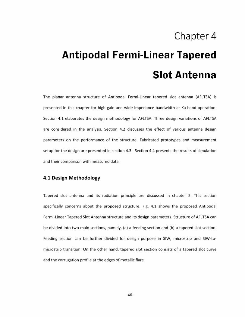
- 46 -
Chapter 4
The planar antenna structure of Antipodal Fermi-Linear tapered slot antenna (AFLTSA) is
presented in this chapter for high gain and wide impedance bandwidth at Ka-band operation.
Section 4.1 elaborates the design methodology for AFLTSA. Three design variations of AFLTSA
are considered in the analysis. Section 4.2 discusses the effect of various antenna design
parameters on the performance of the structure. Fabricated prototypes and measurement
setup for the design are presented in section 4.3. Section 4.4 presents the results of simulation
and their comparison with measured data.
4.1 Design Methodology
Tapered slot antenna and its radiation principle are discussed in chapter 2. This section
specifically concerns about the proposed structure. Fig. 4.1 shows the proposed Antipodal
Fermi-Linear Tapered Slot Antenna structure and its design parameters. Structure of AFLTSA can
be divided into two main sections, namely, (a) a feeding section and (b) a tapered slot section.
Feeding section can be further divided for design purpose in SIW, microstrip and SIW-to-
microstrip transition. On the other hand, tapered slot section consists of a tapered slot curve
and the corrugation profile at the edges of metallic flare.
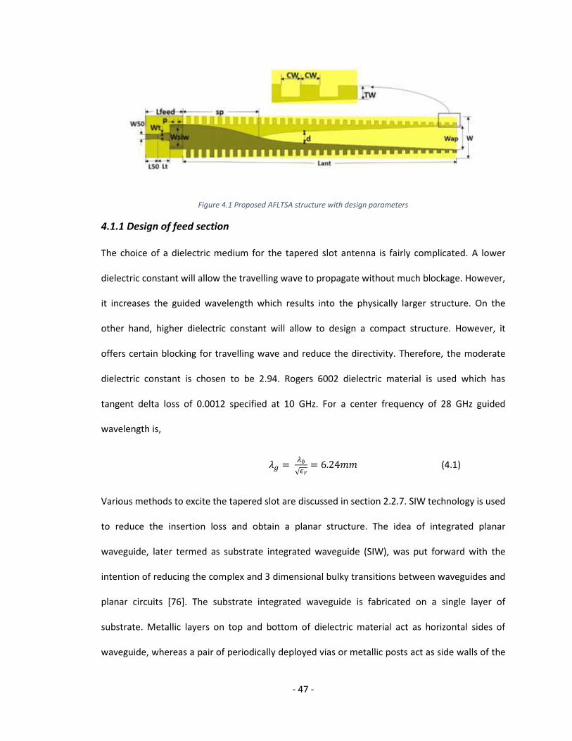
- 47 -
Figure 4.1 Proposed AFLTSA structure with design parameters
4.1.1 Design of feed section
The choice of a dielectric medium for the tapered slot antenna is fairly complicated. A lower
dielectric constant will allow the travelling wave to propagate without much blockage. However,
it increases the guided wavelength which results into the physically larger structure. On the
other hand, higher dielectric constant will allow to design a compact structure. However, it
offers certain blocking for travelling wave and reduce the directivity. Therefore, the moderate
dielectric constant is chosen to be 2.94. Rogers 6002 dielectric material is used which has
tangent delta loss of 0.0012 specified at 10 GHz. For a center frequency of 28 GHz guided
wavelength is,
√ (4.1)
Various methods to excite the tapered slot are discussed in section 2.2.7. SIW technology is used
to reduce the insertion loss and obtain a planar structure. The idea of integrated planar
waveguide, later termed as substrate integrated waveguide (SIW), was put forward with the
intention of reducing the complex and 3 dimensional bulky transitions between waveguides and
planar circuits [76]. The substrate integrated waveguide is fabricated on a single layer of
substrate. Metallic layers on top and bottom of dielectric material act as horizontal sides of
waveguide, whereas a pair of periodically deployed vias or metallic posts act as side walls of the

- 48 -
waveguide, as illustrated in Fig. 4.2. The diameter of the vias (D) and the center to center
distance between successive vias (p), also termed as pitch, are critical design parameters for
substrate integrated waveguide. Pitch should be as small as possible to reduce the leakage
through side walls [77]. Following two criteria ensure that there is no radiation loss from side
walls of SIW,
(4.2)
(4.3)
Figure 4.2 Substrate integrated waveguide design
The cut-off frequency is dependent on effective width of SIW (Weff) and effective relative
permittivity (εr) of the dielectric material as discussed in [78] by following formula,
√ (4.4)
If Wsiw, as shown in Fig. 4.2, is the physical width of SIW, then Weff of the SIW is between (Wsiw –
D) and Wsiw. For higher values of diameter (D), Weff is dependent on physical width of SIW (Wsiw),
pitch (p) and diameter (D) of vias by following relation [79],
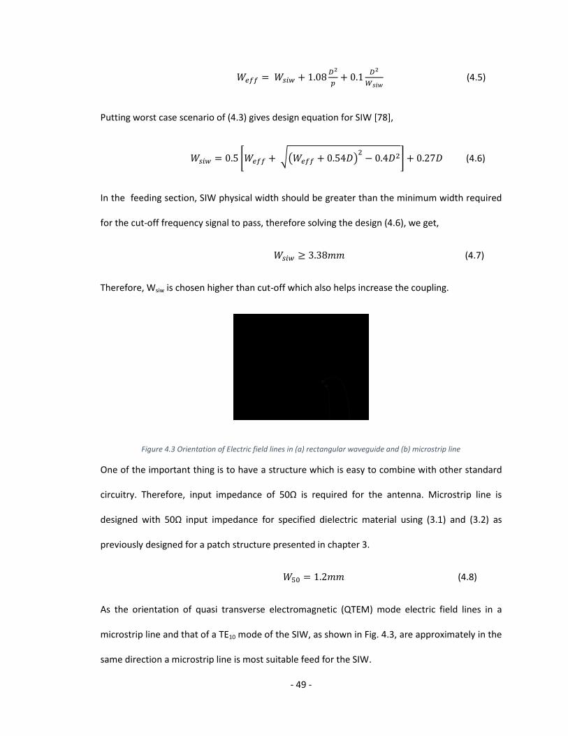
- 49 -
(4.5)
Putting worst case scenario of (4.3) gives design equation for SIW [78],
[ √( ) ] (4.6)
In the feeding section, SIW physical width should be greater than the minimum width required
for the cut-off frequency signal to pass, therefore solving the design (4.6), we get,
(4.7)
Therefore, Wsiw is chosen higher than cut-off which also helps increase the coupling.
Figure 4.3 Orientation of Electric field lines in (a) rectangular waveguide and (b) microstrip line
One of the important thing is to have a structure which is easy to combine with other standard
circuitry. Therefore, input impedance of 50Ω is required for the antenna. Microstrip line is
designed with 50Ω input impedance for specified dielectric material using (3.1) and (3.2) as
previously designed for a patch structure presented in chapter 3.
(4.8)
As the orientation of quasi transverse electromagnetic (QTEM) mode electric field lines in a
microstrip line and that of a TE10 mode of the SIW, as shown in Fig. 4.3, are approximately in the
same direction a microstrip line is most suitable feed for the SIW.
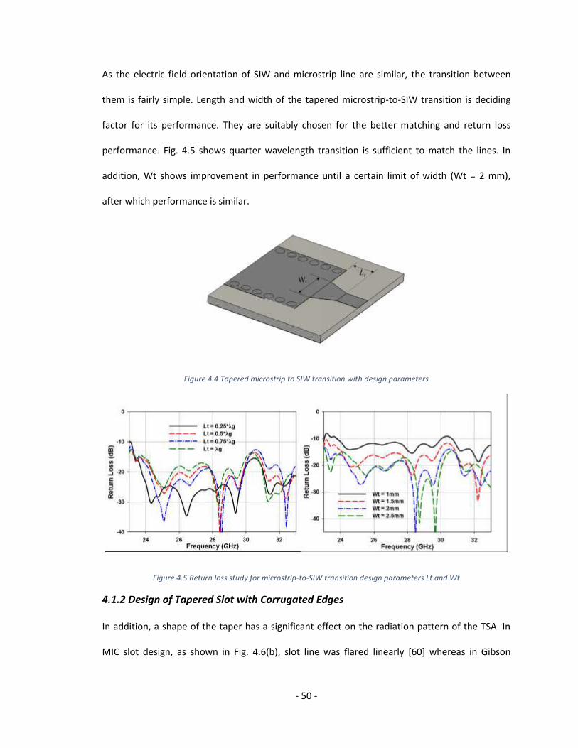
- 50 -
As the electric field orientation of SIW and microstrip line are similar, the transition between
them is fairly simple. Length and width of the tapered microstrip-to-SIW transition is deciding
factor for its performance. They are suitably chosen for the better matching and return loss
performance. Fig. 4.5 shows quarter wavelength transition is sufficient to match the lines. In
addition, Wt shows improvement in performance until a certain limit of width (Wt = 2 mm),
after which performance is similar.
Figure 4.4 Tapered microstrip to SIW transition with design parameters
Figure 4.5 Return loss study for microstrip-to-SIW transition design parameters Lt and Wt
4.1.2 Design of Tapered Slot with Corrugated Edges
In addition, a shape of the taper has a significant effect on the radiation pattern of the TSA. In
MIC slot design, as shown in Fig. 4.6(b), slot line was flared linearly [60] whereas in Gibson

- 51 -
design [61], as shown in Fig. 4.6(a), narrow slot was flared towards aperture using following
exponential equation:
(4.9)
Figure 4.6 (a) Vivaldi (b) Linear (c) Fermi shaped Tapered Slot Antenna
While LTSA has a narrower beamwidth than Vivaldi, it has higher side lobe levels than Vivaldi
[61]. In order to improve the side lobe levels in H plane of TSA, Sugawara et el. introduced Fermi
Tapered Slot Antenna (FTSA) [80], as shown in Fig. 4.6(c). In FTSA, the taper of the slot follows
the following curve:
(4.10)
in this equation, a, b and c are constants which decide the slope, length and width of the curve.
In proposed structure, tapered slot is divided in two parts fermi curve and linear extension. The
maximum part of electric field present in SIW should be coupled into the tapered slot.
Therefore, fermi distribution of the curve is utilized in the initial part of the tapered slot. Fermi
distribution follows (4.10). Shape of this curve serve the important function in this structure as it
increases the coupling between SIW and tapered slot.
In order to, generate the radiation from TSA, its aperture width Wap should be greater than half
a wavelength at the lowest cut-off frequency. However, if the fermi distribution curve is
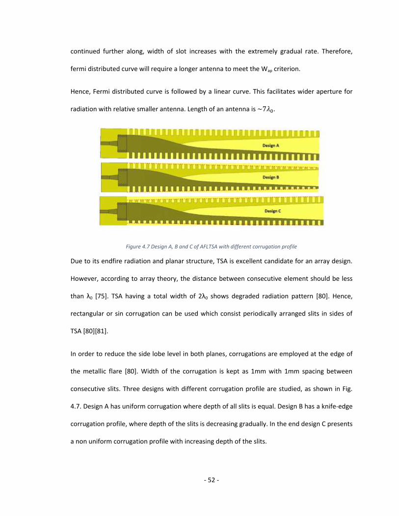
- 52 -
continued further along, width of slot increases with the extremely gradual rate. Therefore,
fermi distributed curve will require a longer antenna to meet the Wap criterion.
Hence, Fermi distributed curve is followed by a linear curve. This facilitates wider aperture for
radiation with relative smaller antenna. Length of an antenna is .
Figure 4.7 Design A, B and C of AFLTSA with different corrugation profile
Due to its endfire radiation and planar structure, TSA is excellent candidate for an array design.
However, according to array theory, the distance between consecutive element should be less
than λ0 [75]. TSA having a total width of 2λ0 shows degraded radiation pattern [80]. Hence,
rectangular or sin corrugation can be used which consist periodically arranged slits in sides of
TSA [80][81].
In order to reduce the side lobe level in both planes, corrugations are employed at the edge of
the metallic flare [80]. Width of the corrugation is kept as 1mm with 1mm spacing between
consecutive slits. Three designs with different corrugation profile are studied, as shown in Fig.
4.7. Design A has uniform corrugation where depth of all slits is equal. Design B has a knife-edge
corrugation profile, where depth of the slits is decreasing gradually. In the end design C presents
a non uniform corrugation profile with increasing depth of the slits.
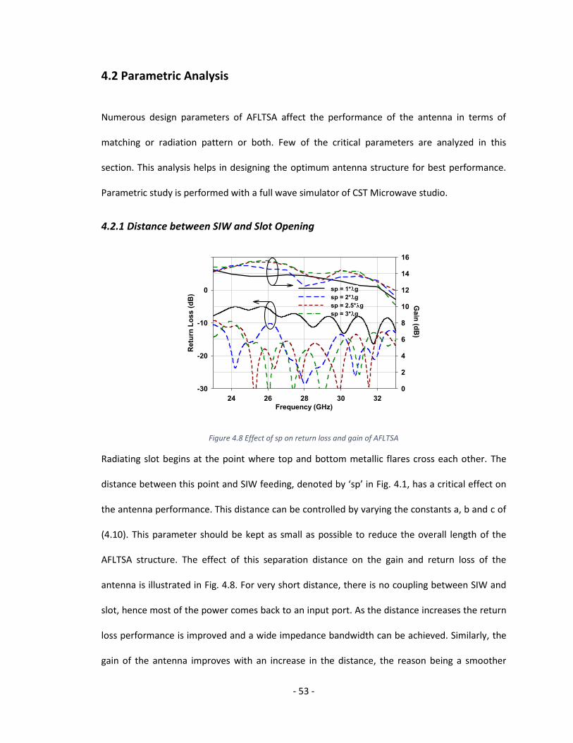
- 53 -
4.2 Parametric Analysis
Numerous design parameters of AFLTSA affect the performance of the antenna in terms of
matching or radiation pattern or both. Few of the critical parameters are analyzed in this
section. This analysis helps in designing the optimum antenna structure for best performance.
Parametric study is performed with a full wave simulator of CST Microwave studio.
4.2.1 Distance between SIW and Slot Opening
Figure 4.8 Effect of sp on return loss and gain of AFLTSA
Radiating slot begins at the point where top and bottom metallic flares cross each other. The
distance between this point and SIW feeding, denoted by ‘sp’ in Fig. 4.1, has a critical effect on
the antenna performance. This distance can be controlled by varying the constants a, b and c of
(4.10). This parameter should be kept as small as possible to reduce the overall length of the
AFLTSA structure. The effect of this separation distance on the gain and return loss of the
antenna is illustrated in Fig. 4.8. For very short distance, there is no coupling between SIW and
slot, hence most of the power comes back to an input port. As the distance increases the return
loss performance is improved and a wide impedance bandwidth can be achieved. Similarly, the
gain of the antenna improves with an increase in the distance, the reason being a smoother
Frequency (GHz)
24 26 28 30 32
Retu
rn L
oss (
dB
)
-30
-20
-10
0
10
Gain
(dB
)
0
2
4
6
8
10
12
14
16
sp = 1* g
sp = 2* g
sp = 2.5* g
sp = 3* g

- 54 -
transition between SIW and slot. Therefore, this distance is chosen to be sufficient for coupling
and small enough for reducing the length of an AFLTSA.
4.2.2 Separation between End Points of Fermi Curve
The separation between the end points of fermi curve, denoted by ‘d’ in Fig. 4.1, basically
controls the opening of a tapered slot. The effect of this distance on the gain of the AFLTSA is
shown in Fig. 4.9. It can be seen that as slot opening increases the gain of the antenna increases
linearly. However, as the width of the antenna is limited, we cannot increase this distance
beyond a certain limit. Therefore, this distance is chosen to be optimum for easy design and
maximum gain.
Figure 4.9 Effect of d on realized gain of the AFLTSA
4.2.3 Width of Corrugation
It has been presented in literature that corrugation alongside the tapered slot improve the side
lobe levels in the radiation pattern. Generally, extremely narrow corrugations are employed at
the edge of TSA [65][80]. Fig. 4.10 shows the effect of corrugation width on the side lobe level in
both planes. It can be seen that having corrugation width greater than deteriorates
the side lobe level rapidly. However, the lesser corrugation width does not have a large effect.
d/ g
0.3 0.4 0.5 0.6 0.7
Realized
Gain
(d
B)
13.8
14.0
14.2
14.4
14.6
14.8
15.0
15.2
15.4
Gain
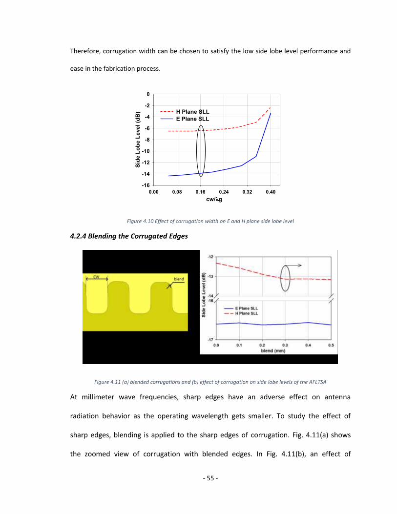
- 55 -
Therefore, corrugation width can be chosen to satisfy the low side lobe level performance and
ease in the fabrication process.
Figure 4.10 Effect of corrugation width on E and H plane side lobe level
4.2.4 Blending the Corrugated Edges
Figure 4.11 (a) blended corrugations and (b) effect of corrugation on side lobe levels of the AFLTSA
At millimeter wave frequencies, sharp edges have an adverse effect on antenna
radiation behavior as the operating wavelength gets smaller. To study the effect of
sharp edges, blending is applied to the sharp edges of corrugation. Fig. 4.11(a) shows
the zoomed view of corrugation with blended edges. In Fig. 4.11(b), an effect of
cw/ g
0.00 0.08 0.16 0.24 0.32 0.40
Sid
e L
ob
e L
evel (d
B)
-16
-14
-12
-10
-8
-6
-4
-2
0
H Plane SLL
E Plane SLL

- 56 -
blending can be seen on a side lobe level in E and H planes. E plane side lobe level
improvement of 1 dB is observed with blending of 0.3mm. However, no effect was
observed on H plane side lobe level performance due to the blending of edges. In
addition, for blending of more than 0.3 mm, there is no improvement as sharp edges are
already vanished.
4.3 Prototypes and Measurement Setup
Various antenna parameters and optimized dimensions of the same are given Table (4.1).
Table 4.1 Design parameters and dimensions of AFLTSA
Design Parameter Dimension in millimeters
Length of Antenna (Lant) 74
Length of feed (Lfeed) 9.5
Width of AFLTSA (W) 10.25
Width of corrugation (Wf) 1
Width of SIW (WSIW) 5.4
Width of aperture 6.2
Width of microstrip 1.2
Diameter of via 0.5
Pitch of SIW 0.86
AFLTSA structure prototypes, shown in Fig. 4.12, for all three designs of corrugation profile are
fabricated using printed circuit board technology. Rogers 6002 dielectric material is used with
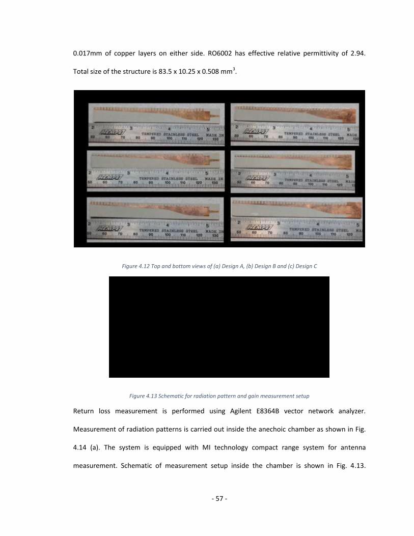
- 57 -
0.017mm of copper layers on either side. RO6002 has effective relative permittivity of 2.94.
Total size of the structure is 83.5 x 10.25 x 0.508 mm3.
Figure 4.12 Top and bottom views of (a) Design A, (b) Design B and (c) Design C
Figure 4.13 Schematic for radiation pattern and gain measurement setup
Return loss measurement is performed using Agilent E8364B vector network analyzer.
Measurement of radiation patterns is carried out inside the anechoic chamber as shown in Fig.
4.14 (a). The system is equipped with MI technology compact range system for antenna
measurement. Schematic of measurement setup inside the chamber is shown in Fig. 4.13.
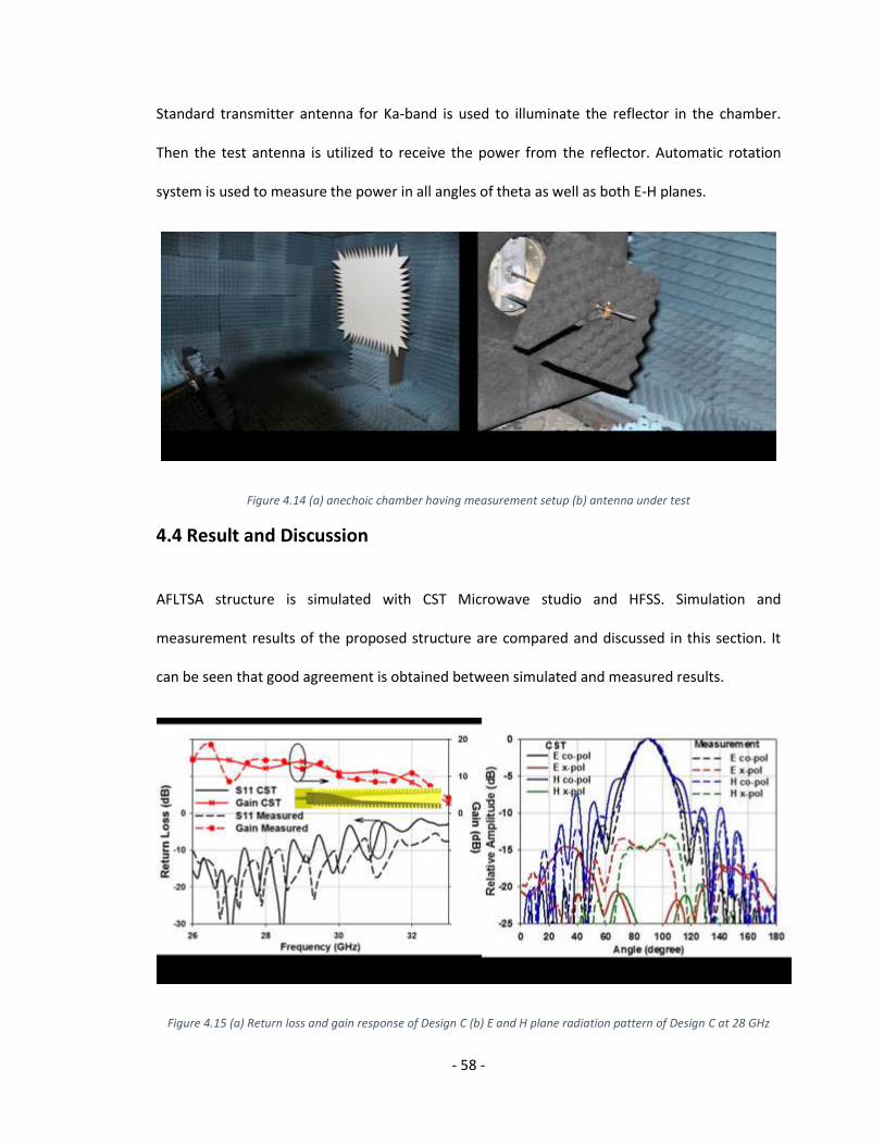
- 58 -
Standard transmitter antenna for Ka-band is used to illuminate the reflector in the chamber.
Then the test antenna is utilized to receive the power from the reflector. Automatic rotation
system is used to measure the power in all angles of theta as well as both E-H planes.
Figure 4.14 (a) anechoic chamber having measurement setup (b) antenna under test
4.4 Result and Discussion
AFLTSA structure is simulated with CST Microwave studio and HFSS. Simulation and
measurement results of the proposed structure are compared and discussed in this section. It
can be seen that good agreement is obtained between simulated and measured results.
Figure 4.15 (a) Return loss and gain response of Design C (b) E and H plane radiation pattern of Design C at 28 GHz

- 59 -
Design C exhibits higher return loss at higher frequencies, as shown in Fig. 4.15(a). Similarly, its
performance degrades at higher frequencies as gain drops below 5 dB level. This has been
resulted due to leakage of an electric field from the edges of a tapered slot region where the
depth of corrugation is not enough. An electric field distribution in 2D plane cut of Design C,
shown in Fig. 4.16, demonstrates the leakage through edges.
Figure 4.16 2D plane cut view of the Design C showing an electric field distribution
Radiation pattern for Design C, given by Fig. 4.15(b), shows the symmetric radiation pattern until
-5 dB level. Design C exhibits E plane side lobe level of -7.8 dB whereas that of H plane is -6 dB.
Cross-polarization level for design C is measured to be around -13 dB.
Figure 4.17 (a) Return loss and gain response of Design A (b) E and H plane radiation pattern of Design A at 28 GHz
Design A has much better matching performance than Design C. It exhibits the wide impedance
bandwidth, illustrated in Fig. 4.17(a), having return loss level of -15 dB or below. It has flat gain
over the entire frequency band at 15 dB level. Radiation pattern in Fig. 4.17(b) for Design A,
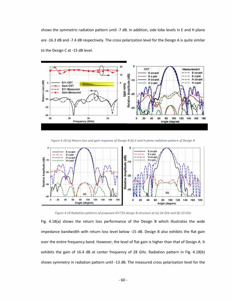
- 60 -
shows the symmetric radiation pattern until -7 dB. In addition, side lobe levels in E and H plane
are -16.3 dB and -7.4 dB respectively. The cross polarization level for the Design A is quite similar
to the Design C at -15 dB level.
Figure 4.18 (a) Return loss and gain response of Design B (b) E and H plane radiation pattern of Design B
Figure 4.19 Radiation patterns of proposed AFLTSA design B structure at (a) 26 GHz and (b) 33 GHz
Fig. 4.18(a) shows the return loss performance of the Design B which illustrates the wide
impedance bandwidth with return loss level below -15 dB. Design B also exhibits the flat gain
over the entire frequency band. However, the level of flat gain is higher than that of Design A. It
exhibits the gain of 16.4 dB at center frequency of 28 GHz. Radiation pattern in Fig. 4.18(b)
shows symmetry in radiation pattern until -13 dB. The measured cross polarization level for the

- 61 -
Design B is improved to -22 dB in both measured planes. Design B has an improved side lobe
level of -19.5 dB in E plane and -13.9 dB in H plane.
Fig. 4.19 shows the radiation pattern of design B at lower and higher end frequencies. There is
no significant effect on the radiation characteristics of the AFLTSA was observed for lower
frequencies. However, at higher frequencies, half power beam width in H plane increases,
hence, symmetry in radiation pattern is not maintained. In addition, side lobe levels of both E
and H plane are increasing at higher frequency.
Figure 4.20 Electric field distribution at aperture of the AFLTSA design A, B and C
To understand the difference in radiation performance of these designs, electric field
distribution at the aperture, shown in Fig. 4.20, should be considered in detail. Typically an
electric field inside the substrate at the aperture of a tapered slot antenna should be in
horizontal direction. However, in a region where the substrate is covered with metal, the
electric field tends to be vertical. This introduces impurity in an ideal behavior of the electric
field. Design A and Design C have metallic corrugation with high depth at the aperture whereas
Design B has small depth metallic corrugation at the aperture. Therefore, Design A and Design C
show a large disturbance in electric field at places marked by circles. The electric field is almost
vertical at these places. On the other hand, Design B has a knife edge model which results in an
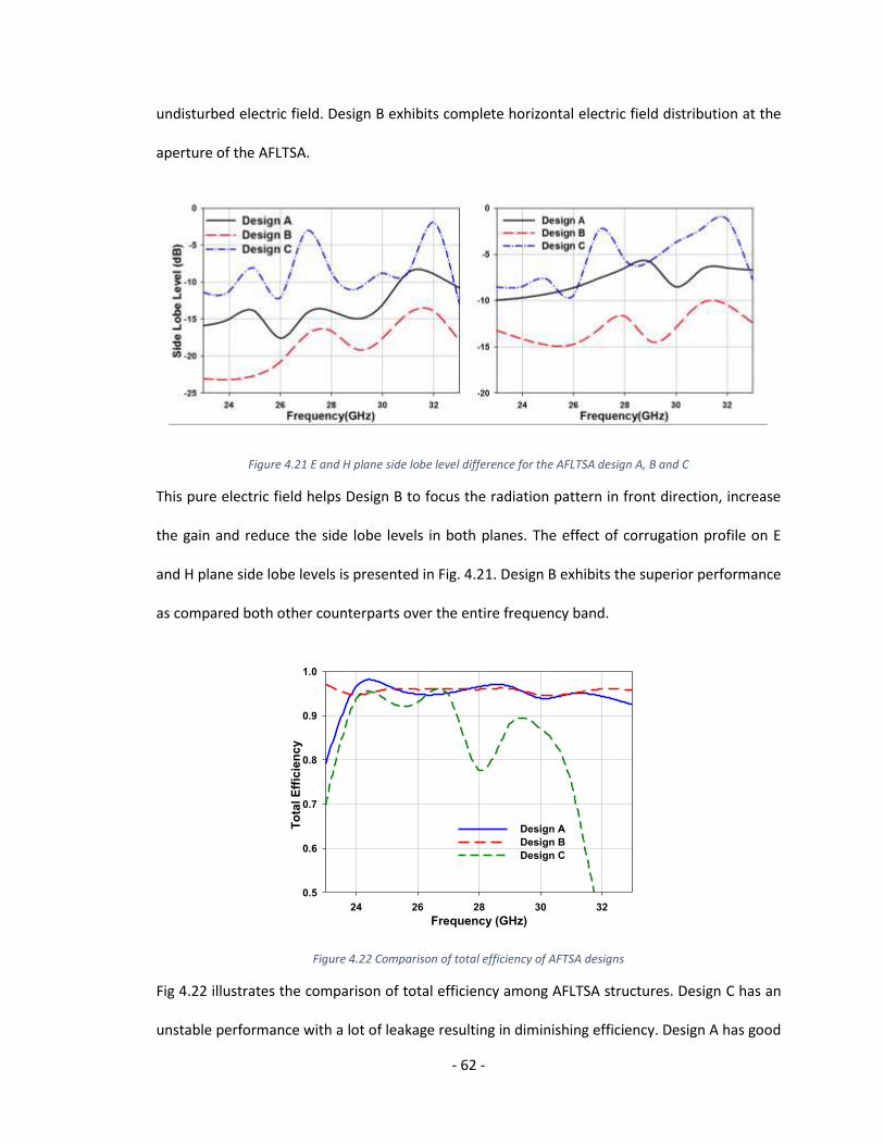
- 62 -
undisturbed electric field. Design B exhibits complete horizontal electric field distribution at the
aperture of the AFLTSA.
Figure 4.21 E and H plane side lobe level difference for the AFLTSA design A, B and C
This pure electric field helps Design B to focus the radiation pattern in front direction, increase
the gain and reduce the side lobe levels in both planes. The effect of corrugation profile on E
and H plane side lobe levels is presented in Fig. 4.21. Design B exhibits the superior performance
as compared both other counterparts over the entire frequency band.
Figure 4.22 Comparison of total efficiency of AFTSA designs
Fig 4.22 illustrates the comparison of total efficiency among AFLTSA structures. Design C has an
unstable performance with a lot of leakage resulting in diminishing efficiency. Design A has good
Frequency (GHz)
24 26 28 30 32
To
tal E
ffic
ien
cy
0.5
0.6
0.7
0.8
0.9
1.0
Design A
Design B
Design C

- 63 -
efficient response except at lower frequencies where its efficiency drops drastically. However,
Design B has stable and efficient performance throughout the frequency of operation. It exhibits
the total efficiency of 95%.
Table 4.2 Comparison of proposed AFLTSA structure with endfire radiating antennas in literature
Antenna Structure Frequency (GHz) Electrical Size Gain (dB)
Luneberg Lens [38] 29-32
13λ x 12λ x 0.5λ 15-16
CPW fed horn [30] 56-63 5λ x 4λ x 0.4λ 14.2
Coax fed SIW horn [32] 27-28 2λ x 1λ x 0.25λ 5.88
WG fed planar horn [31] 84 9λ x 1.5λ x 0.03λ 9
PTFE SIW horn [33] 22-29 3.2λ x 1.8λ x 0.32λ 8
SIW + horn + TSA [35] 80 3λ x 2λ x 0.15λ 14
Diel. Loaded SIW horn [28] 26-27 3λ x 1.5λ x 0.25λ 12
Hemisphere lens [39] 57-65 NA 21
Linear taper diel. Rod [43] 81 40λ x 4λ x 0.1λ 18.4
Step taper diel. Rod [41] 80-90 4λ x 0.4λ x 0.2λ 13
CPW+SIW+ALTSA [64] 21-31 9λ x 1λ x 0.015λ 15
Proposed AFLTSA structure 25-33 8λ x 1λ x 0.015λ 15.5-16.4
Table (4.2) shows the comparison of a realized gain of numerous millimeter wave antenna
structures discussed in the literature for endfire radiation. It can be seen that a proposed
structure offers higher gain than most of the structures discussed in the literature. Antennas
included here operate at frequencies between 5 to 90 GHz range. Although hemisphere shaped
lens antenna and linearly tapered dielectric rod antenna offer higher gain than the proposed
structure, they have non-planar structure which limits its applications and deviates from our
objective.

- 64 -
Chapter 5
5.1 Conclusion
Ka band (26.5-40 GHz) of MMW frequency is utilized for antenna structure designs. High gain
antenna structures are presented to compensate for atmospheric attenuation at Ka band.
Printed circuit board technology is used to fabricate two antenna structures. Theoretical design
is carried out which is followed by EM simulations to optimize the antenna structure
dimensions. Prototypes are fabricated and measurements are performed in anechoic chambers
to verify the performance of the designed structures.
Four-element patch antenna is presented for Ka band. The proposed structure exhibits high gain
of 13.8 dB in broadside direction. An implementation of the air-gap cavity allows it to achieve
the impedance bandwidth of 4.6%. It uses aperture coupling to excite the patch elements which
allows a front to back ratio of 26 dB. The wide beamwidth in the H plane of 700 can be used for
broadcast applications. The proposed structure exhibits a side lobe level of -14.5 dB and -23 dB
in E and H plane, respectively. This structure exhibits the efficiency above 85% in operating
frequency band.
Antipodal fermi linear tapered slot antenna (AFLTSA) is presented for endifire radiation at Ka
band. Proposed structure achieved a flat gain of 16 dB over the entire operating band. Substrate
integrated waveguide technology to feed the tapered slot allows the improvement in return loss
and matching. Furthermore, simple microstrip to substrate integrated waveguide transition
ensures the input impedance of 50Ω can be achieved. It exhibits a wide impedance bandwidth
- 65 -
of 10 GHz in measurement with a return loss level below 15 dB. The proposed structure exhibits
a symmetric radiation pattern till -13 dB level. It has lower side lobe levels of -13.9 dB and -19.5
dB in H and E plane respectively. It also exhibits low cross polarization level of -22 dB. This
efficient antenna structure exhibits the efficiency of 95 % throughout the operating frequency
band. PCB fabrication process makes the design a low cost structure.
5.2 Contribution
Millimeter wave communication has a major role to play in upcoming decades of wireless
communication. Most of the demands of wireless application users can be satisfied by the
millimeter wave communication. This thesis has the following contributions to the millimeter
wave antenna designing field.
1. The designed and fabricated four element patch antenna array [82] achieved a higher
gain (13.8 dB) in a broadside radiation than other planar MMW antenna structures such
as SIW backed transverse slots, miniaturized slots with single director, dielectric
resonator antennas, twin dipole array and other printed antennas.
2. The antipodal fermi linear tapered slot antenna structure, presented for endfire
radiation [83], achieved a higher gain (16.4 dB) than previously proposed MMW planar
antenna structures such as planar horn antennas, dielectric rod antennas, printed yagi
and CPW fed ALTSA. The knife edge corrugation profile for rectangular
corrugation is utilized. The cross polarization level is improved along with side lobe
levels due to knife edge corrugation profile.
3. Width of AFLTSA is smaller than a wavelength which is beneficial in designing multi-
element antenna structures. A novel shape of tapered slot is utilized which allows a
higher gain with shorter antenna structure [84].

- 66 -
5.3 Future Scope
This thesis was focused on the single element design of planar antennas achieving high gain at
Ka band. These structures can be used in multiple-element systems to cover a larger area.
Beam-forming network such as Butler matrix can be used to generate orthogonal beams in
azimuth plane. In this method, the elements are placed such that their peaks are in angular
separation and their 3 dB beamwidths cross each other [20]. Therefore, one wide beam with
high gain of individual elements can be achieved.

- 67 -
[1] G. Falciasecca, “Marconi’s Early Experiments in Wireless Telegraphy, 1895,” IEEE Antennas
and Propagation Magazine, vol. 52, no. 6, pp. 220–221, Dec. 2010.
[2] A. F. Molisch, Wireless Communications, 2nd ed., U.K.: John Wiley & sons Inc., 2011.
[3] P. Bhartia and I. J. Bahl, Millimeter Wave Engineering and Applications, Canada: John Wiley
& sons Inc., 1984.
[4] W. Huang and A. A. Kishk, “Compact dielectric resonator antenna for microwave breast
cancer detection,” IET Microwaves, Antennas Propagation, vol. 3, no. 4, pp. 638–644, Jun.
2009.
[5] E. Topsakal, “Antennas for medical applications: Ongoing research and future challenges,”
in International Conference on Electromagnetics in Advanced Applications. ICEAA ’09, 2009,
pp. 890–893.
[6] L. Frenzel, Communication Electronics: Principles and Applications. McGraw-Hill Companies,
2001.
[7] “IEEE Standard Definitions of Terms for Antennas,” IEEE Std 145-1993, pp. 1–32, Jul. 1993.
[8] “Canadian Table of Frequency Allocations 9 kHz to 275 GHz,” Industry Canada, Canada, Dec.
2009.
[9] C. E. Shannon, A Mathematical Theory of Communication, vol. 27, pp. 379–423, 623–656,
1948.
[10] K. Huang and D. Edwards, Millimetre Wave Antennas for Gigabit wireless communication,
John Wiley and Sons Inc., 2008.
[11] C. A. Balanis, Antenna Theory analysis and design, Third. Ed., USA: John Wiley & sons Inc.,
2005.

- 68 -
[12] A. Goldsmith, Wireless Communications. USA: Cambridge University Press, 2005.
[13] G. Stuber, Principles of Mobile Communication, 3rd ed. Springer, 2011.
[14] T. S. Rappaport, S. Sun, R. Mayzus, H. Zhao, Y. Azar, K. Wang, G. N. Wong, J. K. Schulz, M.
Samimi, and F. Gutierrez, “Millimeter Wave Mobile Communications for 5G Cellular: It Will
Work!,” IEEE Access, vol. 1, pp. 335–349, 2013.
[15] “Key ICT indicators for developed and developing countries and the world (totals and
penetration rates).” Information and Communication Technology (ICT), 2013.
*16+ “Global mobile statistics 2014 Part A: Mobile subscribers; handset market share; mobile
operators,” Available FTP : http://mobithinking.com/mobile-marketing-tools/latest-mobile-
stats/a#uniquesubscribers, Jun-2014. .
[17] “Specific attenuation model for rain for use in prediction method,” RECOMMENDATION ITU-
R P.838-3, 2005.
[18] E-Band Communications, LLC, “E band Technology,” Available FTP : http://www.e-
band.com/index.php?id=86, 2014.
[19] M. Sumi, K. Komiya, R. Yamaguchi, and K. Cho, “Azimuth pattern design to reduce
interference in overlapping sectors using combined tilt,” in 2010 IEEE International
Conference on Wireless Information Technology and Systems (ICWITS), 2010, pp. 1–4.
[20] Z. N. Chen and kwai-man Luk, "Antennas for Base Stations in wireless communications”,
McGraw-Hill Companies, 2009.
[21] J. F. Ramsay, “Microwave Antenna and Waveguide Techniques before 1900,” Proceedings of
the IRE, vol. 46, no. 2, pp. 405–415, Feb. 1958.
[22] M. Skolnik, Introduction to RADAR systems, 3rd ed. Boston: Tata McGraw-Hill Companies,
2001.

- 69 -
[23] S. Preradovic and N. Karmakar, “Chipless millimeter wave identification (MMID) tag at 30
GHz,” in Microwave Conference (EuMC), 2011 41st European, 2011, pp. 123–126.
[24] K. Mizuno, H. Matono, Y. Wagatsuma, H. Warashina, H. Sato, S. Miyanaga, and Y. Yamanaka,
“New applications of millimeter-wave incoherent imaging,” in Microwave Symposium
Digest, 2005 IEEE MTT-S International, 2005, p. 4.
[25] A. Elboushi and A. Sebak, “B14. Active millimeter-wave imaging system for hidden weapons
detection,” in Radio Science Conference (NRSC), 2012, pp. 111–118.
[26] L. Lucci, R. Nesti, G. Pelosi, and S. Selleri, “A Stackable Constant-Width Corrugated Horn
Design for High-Performance and Low-Cost Feed Arrays at Millimeter Wavelengths,” IEEE
Antennas and Wireless Propagation Letters, vol. 11, pp. 1162–1165, 2012.
[27] K. Liu, C. A. Balanis, and G. C. Barber, “Low-loss material coating for horn antenna beam
shaping,” in Antennas and Propagation Society International Symposium, 1991. AP-S. Digest,
vol.3, 1991, pp. 1664–1667.
[28] N. Ghassemi and K. Wu, “Millimeter-Wave Integrated Pyramidal Horn Antenna Made of
Multilayer Printed Circuit Board (PCB) Process,” IEEE Transactions on Antennas and
Propagation, vol. 60, no. 9, pp. 4432–4435, 2012.
[29] H. Wang, D.-G. Fang, B. Zhang, and W.-Q. Che, “Dielectric Loaded Substrate Integrated
Waveguide (SIW) -Plane Horn Antennas,” IEEE Transactions on Antennas and Propagation,
vol. 58, no. 3, pp. 640–647, 2010.
[30] S. Methfessel and L. Schmidt, “Design of a balanced-fed patch-excited horn antenna at
millimeter-wave frequencies,” in 2010 Proceedings of the Fourth European Conference on
Antennas and Propagation (EuCAP), 2010, pp. 1–4.

- 70 -
[31] B. Pan, Y. Li, G. E. Ponchak, J. Papapolymerou, and M. M. Tentzeris, “A 60-GHz CPW-Fed
High-Gain and Broadband Integrated Horn Antenna,” IEEE Transactions on Antennas and
Propagation, vol. 57, no. 4, pp. 1050–1056, 2009.
[32] M. El-Nawawy, A. M. M. A. Allam, and M. Ghoneima, “Design and fabrication of W-band
SIW horn antenna using PCB process,” in 2013 1st International Conference on
Communications, Signal Processing, and their Applications (ICCSPA), 2013, pp. 1–4.
[33] S. A. Razavi and M. H. Neshati, “Low profile H-plane horn antenna based on half mode
substrate integrated waveguide technique,” in 2012 20th Iranian Conference on Electrical
Engineering (ICEE), 2012, pp. 1351–1354.
[34] S. R. Ranade and D. U. Nair, “Design of a substrate integrated waveguide H plane Horn
antenna on a PTFE substrate for automotive radar application,” in 2011 IEEE Applied
Electromagnetics Conference (AEMC), 2011, pp. 1–4.
[35] J. S. Fu, “Preliminary study of 60 GHz air-filled SIW H-plane horn antenna,” in 2011 IEEE
Electrical Design of Advanced Packaging and Systems Symposium (EDAPS), 2011, pp. 1–4.
[36] N. Ghassemi and K. Wu, “Planar High-Gain Dielectric-Loaded Antipodal Linearly Tapered Slot
Antenna for E and W Band Gigabyte Point-to-Point Wireless Services,” IEEE Trans. Antennas
Propag., vol. 61, no. 4, pp. 1747–1755, 2013.
[37] W. Che, B. Fu, P. Yao, Y. L. Chow, and E. K. N. Yung, “A compact substrate integrated
waveguide H-plane horn antenna with dielectric arc lens,” International Journal of RF and
Microwave Computer-Aided Engineering, vol. 17, no. 5, pp. 473–479, 2007.
[38] B. Fuchs, O. Lafond, S. Rondineau, and M. Himdi, “Design and characterization of half
Maxwell fish-eye lens antennas in millimeter waves,” IEEE Transactions on Microwave
Theory and Techniques, vol. 54, no. 6, pp. 2292–2300, Jun. 2006.

- 71 -
[39] C. Hua, X. Wu, and W. Wu, “A millimeter-wave cylindrical modified Luneberg lens antenna,”
in Microwave Symposium Digest (MTT), 2012 IEEE MTT-S International, 2012, pp. 1–3.
[40] C. A. Fernandes, R. C. Martins, T. Radil, P. M. Ramos, E. B. Lima, C. R. Medeiros, and J. R.
Costa, “Low-cost mechanically steered millimeter-wave lens antenna system for indoor
LANs,” in 2010 International Workshop on Antenna Technology (iWAT), 2010, pp. 1–4.
[41] R. E. Collin and F. J. Zucker, Antenna Theory Part 2, vol. 7, USA: McGraw-Hill Companies,
1969.
[42] Q. Chen, C. Wang, B. Liu, Q. Sun, and Y. Zhao, “Dielectric step-tapered rod antenna array for
millimeter waves,” in 2011 36th International Conference on Infrared, Millimeter and
Terahertz Waves (IRMMW-THz), 2011, pp. 1–2.
[43] S. Xu and X. Wu, “A millimeter-wave omnidirectional dielectric rod metallic grating
antenna,” IEEE Transactions on Antennas and Propagation, vol. 44, no. 1, pp. 74–79, Jan.
1996.
[44] S. Kobayashi, R. Mittra, and R. Lampe, “Dielectric tapered rod antennas for millimeter-wave
applications,” IEEE Transactions on Antennas and Propagation, vol. 30, no. 1, pp. 54–58, Jan.
1982.
[45] Y. Shiau, “Dielectric Rod Antennas for Millimeter-Wave Integrated Circuits (Short Papers),”
IEEE Transactions on Microwave Theory and Techniques, vol. 24, no. 11, pp. 869–872, Nov.
1976.
[46] R. Kazemi, A. E. Fathy, and R. A. Sadeghzadeh, “Dielectric Rod Antenna Array With Substrate
Integrated Waveguide Planar Feed Network for Wideband Applications,” IEEE Transactions
on Antennas and Propagation, vol. 60, no. 3, pp. 1312–1319, 2012.

- 72 -
[47] J. Liu, D. R. Jackson, and Y. Long, “Substrate Integrated Waveguide (SIW) Leaky-Wave
Antenna With Transverse Slots,” IEEE Transactions on Antennas and Propagation, vol. 60,
no. 1, pp. 20–29, 2012.
[48] H. Han, Y. Wang, X. Liu, and H. Guo, “Miniaturized high gain slot antenna with single-layer
director,” in 2013 Proceedings of the International Symposium on Antennas Propagation
(ISAP), 2013, vol. 01, pp. 265–268.
[49] L. Goldstone and A. A. Oliner, “Leaky-wave antennas I: Rectangular waveguides,” IRE
Transactions on Antennas and Propagation, vol. 7, no. 4, pp. 307–319, Oct. 1959.
[50] P. Lampariello, “New millimeter-wave leaky-wave antennas,” in Microwave Conference
Proceedings, 1997. APMC ’97, 1997 Asia-Pacific, 1997, vol. 1, pp. 405–408.
[51] M. K. Brar and S. K. Sharma, “A wideband aperture-coupled pentagon shape dielectric
resonator antenna (DRA) for wireless communication applications,” in 2011 IEEE
International Symposium on Antennas and Propagation (APSURSI), 2011, pp. 1674–1677.
[52] Q. Lai, C. Fumeaux, W. Hong, and R. Vahldieck, “60 GHz Aperture-Coupled Dielectric
Resonator Antennas Fed by a Half-Mode Substrate Integrated Waveguide,” IEEE
Transactions on Antennas and Propagation, vol. 58, no. 6, pp. 1856–1864, 2010.
[53] W. M. Abdel-Wahab and S. Safavi-Naeini, “Improvement of aperture coupling in SIW-fed
DRA using embedded metallic posts,” in 2012 IEEE Antennas and Propagation Society
International Symposium (APSURSI), 2012, pp. 1–2.
[54] G. R. DeJean and M. M. Tentzeris, “A New High-Gain Microstrip Yagi Array Antenna With a
High Front-to-Back (F/B) Ratio for WLAN and Millimeter-Wave Applications,” IEEE
Transactions on Antennas and Propagation, vol. 55, no. 2, pp. 298–304, Feb. 2007.

- 73 -
[55] K.-F. Hung and Y.-C. Lin, “Broadband printed circularly-polarised aperture antenna array for
millimetre-wave gigabit applications,” Electronics Letters, vol. 44, no. 25, pp. 1439–1441,
Dec. 2008.
[56] Z. Briqech and A. Sebak, “Low-cost 60 GHz printed Yagi antenna array,” in 2012 IEEE
Antennas and Propagation Society International Symposium (APSURSI), 2012, pp. 1–2.
[57] Y.-H. Suh and K. Chang, “A new Millimeter-wave printed dipole phased array antenna using
microstrip-fed coplanar stripline tee junctions,” IEEE Transactions on Antennas and
Propagation, vol. 52, no. 8, pp. 2019–2026, Aug. 2004.
[58] R. B. Waterhouse, D. Novak, A. Nirmalathas, and C. Lim, “Broadband printed millimeter-
wave antennas,” IEEE Transactions on Antennas and Propagation, vol. 51, no. 9, pp. 2492–
2495, Sep. 2003.
[59] H. Wong, K. B. Ng, C. H. Chan, and K. M. Luk, “Printed antennas for millimeter-wave
applications,” in 2013 International Workshop on Antenna Technology (iWAT), 2013, pp.
411–414.
[60] S. N. Prasad and S. Mahapatra, “A Novel MIC Slot-Line Antenna,” in Microwave Conference,
1979. 9th European, 1979, pp. 120–124.
[61] P. J. Gibson, “The Vivaldi Aerial,” in Microwave Conference, 1979. 9th European, 1979, pp.
101–105.
[62] R. N. Simons, R. Q. Lee, and T. D. Perl, “Non-planar linearly tapered slot antennas with
balanced microstrip feed,” in , IEEE Antennas and Propagation Society International
Symposium, 1992. AP-S. 1992 Digest. Held in Conjuction with: URSI Radio Science Meeting
and Nuclear EMP Meeting, 1992, pp. 2109–2112 vol.4.

- 74 -
[63] D. H. Schaubert, E. L. Kollberg, T. Korzeniowski, T. Thungren, J. Johansson, and K. S.
Yngvesson, “Endfire tapered slot antennas on dielectric substrates,” IEEE Transactions on
Antennas and Propagation, vol. 33, no. 12, pp. 1392–1400, 1985.
[64] Z.-C. Hao, W. Hong, J. Chen, X.-P. Chen, and K. Wu, “A novel feeding technique for antipodal
linearly tapered slot antenna array,” in Microwave Symposium Digest, 2005 IEEE MTT-S
International, 2005.
[65] F. Taringou, D. Dousset, J. Bornemann, and K. Wu, “Broadband CPW Feed for Millimeter-
Wave SIW-Based Antipodal Linearly Tapered Slot Antennas,” IEEE Transactions on Antennas
and Propagation, vol. 61, no. 4, pp. 1756–1762, 2013.
[66] R. Booton, Computational Methods for Electromagnetics and Microwaves. USA: John Wiley
& sons Inc., 1992.
[67] D. Davidson, “An overview of Computational Electromagnetics for RF and Microwave
applications,” in Computational Electromagnetics for RF and Microwave Engineering,
Second., Cambridge University Press, 2011.
[68] T. Hubbing, “Survey of Numerical Electromagneitc Modeling Techniques,” University of
Mussouri-Rolla, TR91-1-001.3, Sep. 1991.
[69] T. Rylander, A. Bondeson, and P. Ingelstrom, Computational Electromagnetics, Second ed.,
Springer, 2013.
[70] I. Munteanu and T. Weiland, “RF & Microwave Simulation with the Finite Integration
Technique- From Component to System Design,” in Scientific Computing in Electrical
Engineering, Springer, 2007.
[71] D. Pozar, Microwave Engineering, 3rd ed., John Wiley & sons Inc.,2009.

- 75 -
[72] D. Deslandes, “Design equations for tapered microstrip-to-Substrate Integrated Waveguide
transitions,” in Microwave Symposium Digest (MTT), 2010 IEEE MTT-S International, 2010,
pp. 704–707.
[73] K. F. Lee and K. Luk, “Broadbanding Techniques IV - Aperture Coupled Patches,” in
Microstrip Patch Antennas, London: Imperial Colege Press, pp. 291–320, 2011.
[74] F. T. Ulbay, Fundamentals of Applied Electromagnetics. USA: Pearson Education Inc., 2004.
[75] Warren Stutzman and G. Thiele, "Antenna Theory and Design”, Second. John Wiley & sons
Inc., 1998.
[76] D. Deslandes and K. Wu, “Integrated microstrip and rectangular waveguide in planar form,”
IEEE Microw. Wirel. Compon. Lett., vol. 11, no. 2, pp. 68–70, 2001.
[77] K. Wu, D. Deslandes, and Y. Cassivi, “The substrate integrated circuits - a new concept for
high-frequency electronics and optoelectronics,” in 6th International Conference on
Telecommunications in Modern Satellite, Cable and Broadcasting Service, 2003., P–III–P–X
vol.1.
[78] J. E. Rayas-Sanchez and V. Gutierrez-Ayala, “A general EM-based design procedure for
single-layer substrate integrated waveguide interconnects with microstrip transitions,” in
Microwave Symposium Digest, 2008 IEEE MTT-S International, 2008, pp. 983–986.
[79] F. Xu and K. Wu, “Guided-wave and leakage characteristics of substrate integrated
waveguide,” IEEE Trans. Microw. Theory Tech., vol. 53, no. 1, pp. 66–73, 2005.
[80] S. Sugawara, Y. Maita, K. Adachi, K. Mori, and K. Mizuno, “A mm-wave tapered slot antenna
with improved radiation pattern,” in Microwave Symposium Digest, 1997., IEEE MTT-S
International, 1997, vol. 2, pp. 959–962.

- 76 -
[81] Z. Briqech, A. Sebak, and T. A. Denidni, “60 GHz Fermi tapered slot antenna with sin-
corrugation,” in 2013 IEEE Antennas and Propagation Society International Symposium
(APSURSI), 2013, pp. 160–161.
[82] K. Phalak and A. Sebak, “Aperture Coupled Microstrip Patch Antenna Array for High Gain at
Millimeter Waves,” to be presented at the 2014 IEEE International Conference on
Communication, Networks and Satellite, Jakarta, November, 2014.
[83] K. Phalak, Z. Briqech, and A. Sebak, “Ka-Band Antipodal Fermi-Linear Tapered Slot Antenna
with a Knife Edge Corrugation,” Microw. Opt. Technol. Lett., Submitted, 2014.
[84] K. Phalak, Z. Briqech, and A. Sebak, “Substrate Integrated Waveguide fed Antipodal Fermi
Linear Tapered Slot Antenna_at 28 GHz,” presented at 16th international symposium on
antenna technology and applied electromagnetics, in press, 2014.