Embed Size (px)
Citation preview
Nov. 25th -26th, 2014, Moscow
1University of Toronto, Rogers ECE Department
IEEE COMPEL 2016
High-Performance Controllers for Emerging Converter Topologies and Low-Power High-Frequency SMPS
Laboratory for Power Management and Integrated SMPS
University of Toronto, E. Rogers ECE Department
http://www.ele.utoronto.ca/power_management/publications.html
Aleksandar Prodić
E-mail: [email protected]
IEEE COMPEL 2016IEEE PwrSoC 2018
Nov. 25th -26th, 2014, Moscow
2University of Toronto, Rogers ECE Department
IEEE COMPEL 2016IEEE COMPEL 2016
Applications of Primary Interest, Challenges and Goals
IEEE PwrSoC 2018
Nov. 25th -26th, 2014, Moscow
3University of Toronto, Rogers ECE Department
IEEE COMPEL 2016
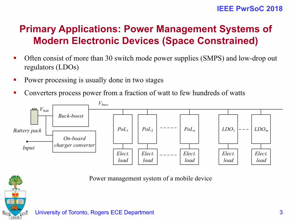
Primary Applications: Power Management Systems of Modern Electronic Devices (Space Constrained)
Buck-boost
On-boardcharger converter
Battery pack
Input
Vbuss
PoL1 PoL2 PoLn LDOmLDO1
Elect. load
Elect. load
Elect. load
Elect. load
Elect. load
Vbatt.
§ Often consist of more than 30 switch mode power supplies (SMPS) and low-drop out regulators (LDOs)
§ Power processing is usually done in two stages
§ Converters process power from a fraction of watt to few hundreds of watts
Power management system of a mobile device
IEEE PwrSoC 2018
Nov. 25th -26th, 2014, Moscow
4University of Toronto, Rogers ECE Department
IEEE COMPEL 2016
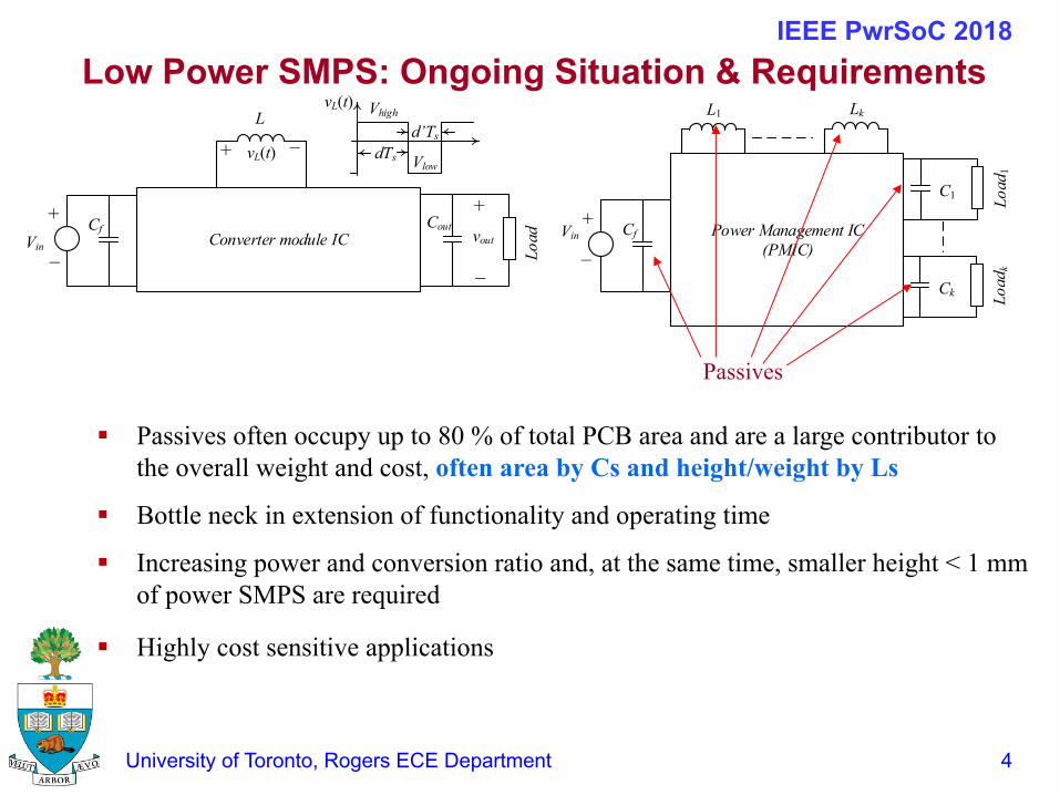
Low Power SMPS: Ongoing Situation & Requirements
Converter module IC
vL(t)+ _
vL(t)
dTs
d’Ts
Vhigh
Vlow
Vin
+
_
L
Cf Cout+
_
vout
Load Power Management IC
(PMIC)Vin
+_
L1
Cf
C1 Load1
Lk
Ck Load
k
§ Passives often occupy up to 80 % of total PCB area and are a large contributor to the overall weight and cost, often area by Cs and height/weight by Ls
§ Bottle neck in extension of functionality and operating time
§ Increasing power and conversion ratio and, at the same time, smaller height < 1 mm of power SMPS are required
§ Highly cost sensitive applications
Passives
IEEE PwrSoC 2018
Nov. 25th -26th, 2014, Moscow
5University of Toronto, Rogers ECE Department
IEEE COMPEL 2016
§ Existing solutions cannot keep with requirements of emerging applications, due to increasing power consumption (driven by increasing functionality)
§ Design requirements practically ask for larger output power and smaller passive components while improving efficiency. Due to thermal (safety and cooling constrains).
§ Related, voltage requirements are changing, higher step down required
§ Custom topological/control solutions for a given application might be needed to maximize efficiency and minimize the volume.
§ Solutions based on novel devices and technologies, i.e. operation at higher switching frequencies
§ Solutions based on novel controller design and power stage architectures => Focus of this talk
Main Requirement for new solutions => Need to be more efficient and smaller at the same time
SMPS in Low Power Applications – General Challenges IEEE PwrSoC 2018
Nov. 25th -26th, 2014, Moscow
6University of Toronto, Rogers ECE Department
IEEE COMPEL 2016IEEE COMPEL 2016
Fundamental Volume Reduction Principles for Passive Components
IEEE PwrSoC 2018
Nov. 25th -26th, 2014, Moscow
7University of Toronto, Rogers ECE Department
IEEE COMPEL 2016IEEE COMPEL 2016
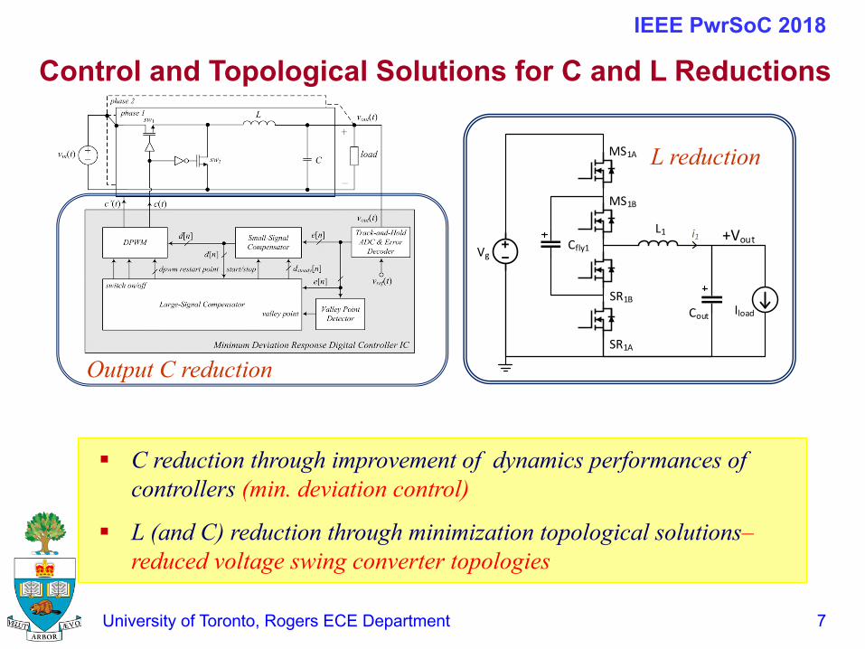
Control and Topological Solutions for C and L Reductions
§ C reduction through improvement of dynamics performances of controllers (min. deviation control)
§ L (and C) reduction through minimization topological solutions–reduced voltage swing converter topologies
IEEE PwrSoC 2018
Cfly1i1L1
Cout
+VoutVg
Iload
MS1A
MS1B
SR1B
SR1A
Output C reduction
L reduction
Nov. 25th -26th, 2014, Moscow
8University of Toronto, Rogers ECE Department
IEEE COMPEL 2016
Single Mode Minimum Deviation Controller
IEEE PwrSoC 2018
Nov. 25th -26th, 2014, Moscow
9University of Toronto, Rogers ECE Department
IEEE COMPEL 2016IEEE COMPEL 2016
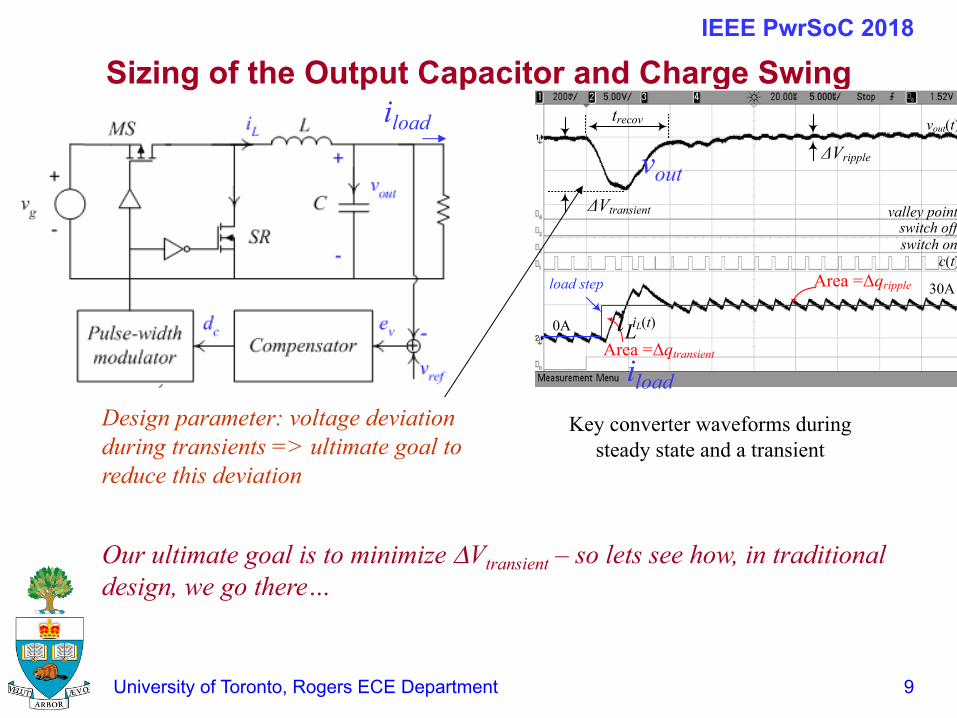
Sizing of the Output Capacitor and Charge Swingtrecov
ΔVtransient
vout(t)
30A
iL(t)
load step
valley pointswitch off switch on
c(t)
0A
Area =Δqtransient
Area =Δqripple
ΔVripple
iload
Key converter waveforms during steady state and a transient
iL
iload
vout
Design parameter: voltage deviation during transients => ultimate goal to reduce this deviation
IEEE PwrSoC 2018
Our ultimate goal is to minimize DVtransient – so lets see how, in traditional design, we go there…
Nov. 25th -26th, 2014, Moscow
10University of Toronto, Rogers ECE Department
IEEE COMPEL 2016
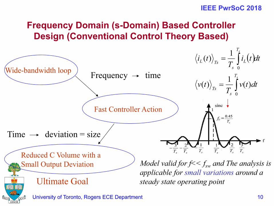
Frequency Domain (s-Domain) Based Controller Design (Conventional Control Theory Based)
Wide-bandwidth loop
Fast Controller Action
Reduced C Volume with a Small Output Deviation
Frequency time
Time deviation = size
Ultimate Goal
IEEE PwrSoC 2018
( )
ò
ò
=
=
s
s
T
sTs
T
Ls
TsL
dttvT
tv
dttiT
ti
0
0
)(1)(
1)(
Model valid for f<< fsw and The analysis is applicable for small variations around a steady state operating point
Nov. 25th -26th, 2014, Moscow
11University of Toronto, Rogers ECE Department
IEEE COMPEL 2016
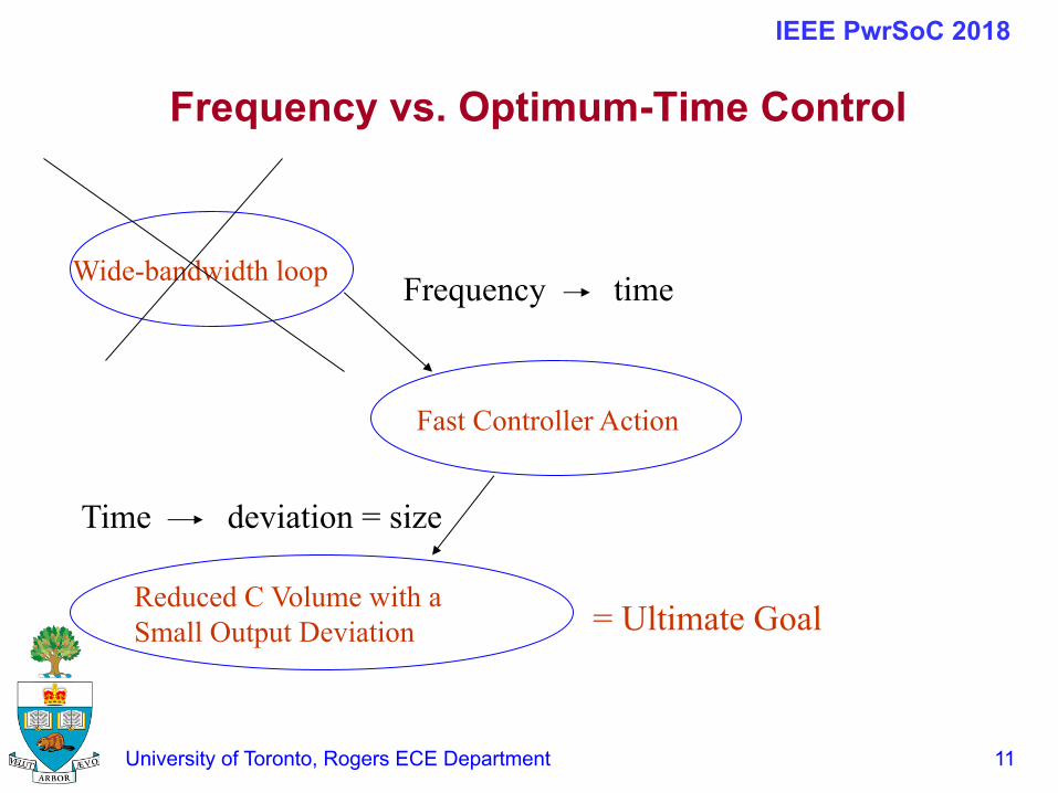
Frequency vs. Optimum-Time Control
Wide-bandwidth loop
Fast Controller Action
Reduced C Volume with a Small Output Deviation
Frequency time
Time deviation = size
= Ultimate Goal
IEEE PwrSoC 2018
Nov. 25th -26th, 2014, Moscow
12University of Toronto, Rogers ECE Department
IEEE COMPEL 2016IEEE COMPEL 2016
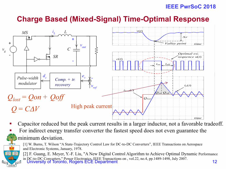
Charge Based (Mixed-Signal) Time-Optimal Responsev(t)
time
time
c(t)
Optimal sw. sequence u(t)
ton toff
iload(t)
iL(t)
Valley point
QoffQon
Dv
Qlost
Comp. + tr. recovery
Qlost = Qon + QoffQ = CDV High peak current
§ Capacitor reduced but the peak current results in a larger inductor, not a favorable tradeoff. § For indirect energy transfer converter the fastest speed does not even guarantee the
minimum deviation. [1] W. Burns, T. Wilson “A State-Trajectory Control Law for DC-to-DC Converters”, IEEE Transactions on Aerospace and Electronic Systems, January, 1978.[2] F. Guang, E. Meyer, Y.-F. Liu, "A New Digital Control Algorithm to Achieve Optimal Dynamic Performance in DC-to-DC Converters," Power Electronics, IEEE Transactions on , vol.22, no.4, pp.1489-1498, July 2007.
IEEE PwrSoC 2018
Nov. 25th -26th, 2014, Moscow
13University of Toronto, Rogers ECE Department
IEEE COMPEL 2016
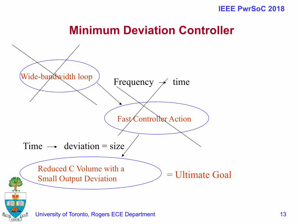
Minimum Deviation Controller
Wide-bandwidth loop
Fast Controller Action
Reduced C Volume with a Small Output Deviation
Frequency time
Time deviation = size
= Ultimate Goal
IEEE PwrSoC 2018
Nov. 25th -26th, 2014, Moscow
14University of Toronto, Rogers ECE Department
IEEE COMPEL 2016
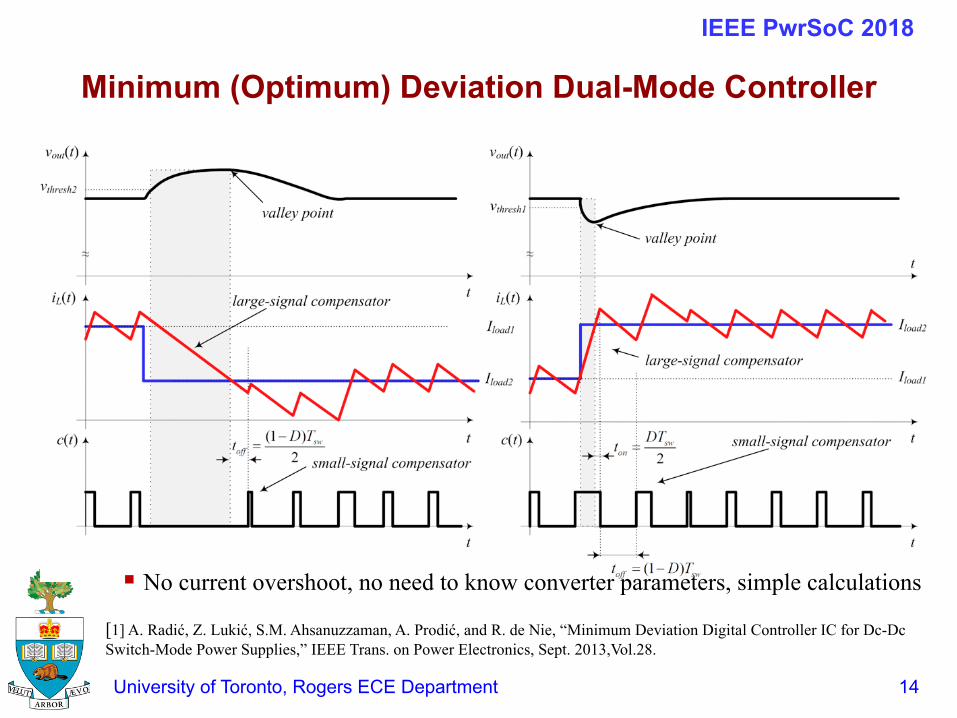
Minimum (Optimum) Deviation Dual-Mode Controller
§ No current overshoot, no need to know converter parameters, simple calculations
[1] A. Radić, Z. Lukić, S.M. Ahsanuzzaman, A. Prodić, and R. de Nie, “Minimum Deviation Digital Controller IC for Dc-Dc Switch-Mode Power Supplies,” IEEE Trans. on Power Electronics, Sept. 2013,Vol.28.
IEEE PwrSoC 2018
Nov. 25th -26th, 2014, Moscow
15University of Toronto, Rogers ECE Department
IEEE COMPEL 2016
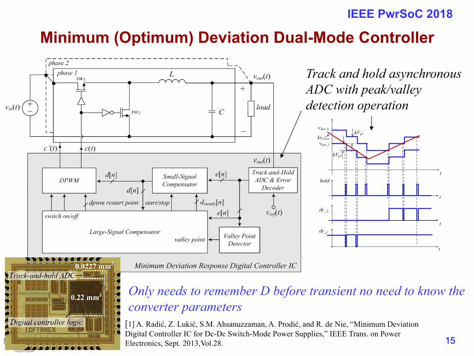
Only needs to remember D before transient no need to know the converter parameters
Minimum (Optimum) Deviation Dual-Mode ControllerIEEE PwrSoC 2018
kverror
hold
t
t
t
kVq1
t
vdyn_h
vdyn_l
dy_h
kVq1
dy_l
[1] A. Radić, Z. Lukić, S.M. Ahsanuzzaman, A. Prodić, and R. de Nie, “Minimum Deviation Digital Controller IC for Dc-Dc Switch-Mode Power Supplies,” IEEE Trans. on Power Electronics, Sept. 2013,Vol.28.
Track and hold asynchronous ADC with peak/valley detection operation
Nov. 25th -26th, 2014, Moscow
16University of Toronto, Rogers ECE Department
IEEE COMPEL 2016
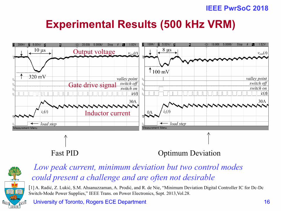
Experimental Results (500 kHz VRM)
Inductor current
Gate drive signal
Output voltage
Fast PID Optimum Deviation
[1] A. Radić, Z. Lukić, S.M. Ahsanuzzaman, A. Prodić, and R. de Nie, “Minimum Deviation Digital Controller IC for Dc-Dc Switch-Mode Power Supplies,” IEEE Trans. on Power Electronics, Sept. 2013,Vol.28.
Low peak current, minimum deviation but two control modes could present a challenge and are often not desirable
IEEE PwrSoC 2018
Nov. 25th -26th, 2014, Moscow
17University of Toronto, Rogers ECE Department
IEEE COMPEL 2016
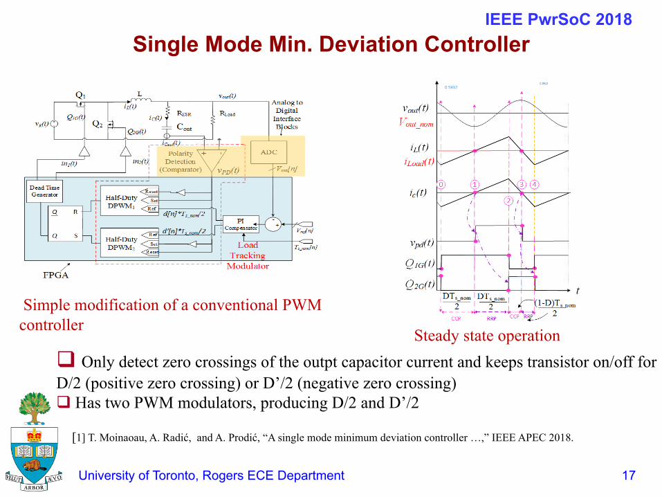
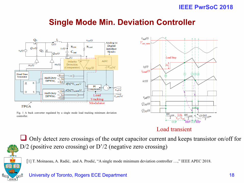
q Only detect zero crossings of the outpt capacitor current and keeps transistor on/off for D/2 (positive zero crossing) or D’/2 (negative zero crossing)q Has two PWM modulators, producing D/2 and D’/2
Single Mode Min. Deviation Controller
[1] T. Moinaoau, A. Radić, and A. Prodić, “A single mode minimum deviation controller …,” IEEE APEC 2018.
Steady state operation
Simple modification of a conventional PWM controller
IEEE PwrSoC 2018
Nov. 25th -26th, 2014, Moscow
18University of Toronto, Rogers ECE Department
IEEE COMPEL 2016
q Only detect zero crossings of the outpt capacitor current and keeps transistor on/off for D/2 (positive zero crossing) or D’/2 (negative zero crossing)
Single Mode Min. Deviation Controller
[1] T. Moinaoau, A. Radić, and A. Prodić, “A single mode minimum deviation controller …,” IEEE APEC 2018.
Fig. 1 A buck converter regulated by a single mode load tracking minimum deviationcontroller.
Load transient
IEEE PwrSoC 2018
Nov. 25th -26th, 2014, Moscow
19University of Toronto, Rogers ECE Department
IEEE COMPEL 2016
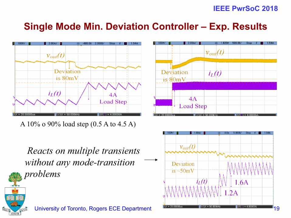
Single Mode Min. Deviation Controller – Exp. Results
A 10% o 90% load step (0.5 A to 4.5 A)
IEEE PwrSoC 2018
Reacts on multiple transients without any mode-transition problems
Nov. 25th -26th, 2014, Moscow
20University of Toronto, Rogers ECE Department
IEEE COMPEL 2016
Inductor Volt-Swing Reduction Based Topologies
IEEE PwrSoC 2018
Nov. 25th -26th, 2014, Moscow
21University of Toronto, Rogers ECE Department
IEEE COMPEL 2016
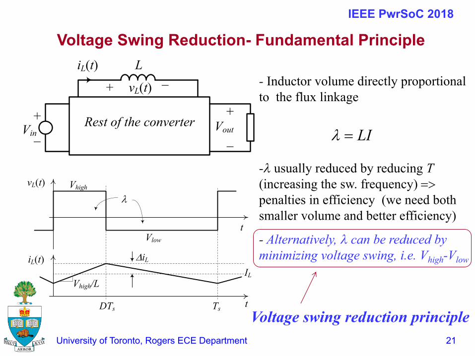
Voltage Swing Reduction- Fundamental Principle
- Inductor volume directly proportional to the flux linkage
-l usually reduced by reducing T (increasing the sw. frequency) =>penalties in efficiency (we need both smaller volume and better efficiency)
- Alternatively, l can be reduced by minimizing voltage swing, i.e. Vhigh-Vlow
Rest of the converter
vL(t)+_
iL(t)
Vin
+_ Vout
+
_
L
Vhigh
Vlow
TsDTs
vL(t)l
iL(t)
Vhigh/L
DiLIL
t
t
LI=l
Voltage swing reduction principle
IEEE PwrSoC 2018
Nov. 25th -26th, 2014, Moscow
22University of Toronto, Rogers ECE Department
IEEE COMPEL 2016
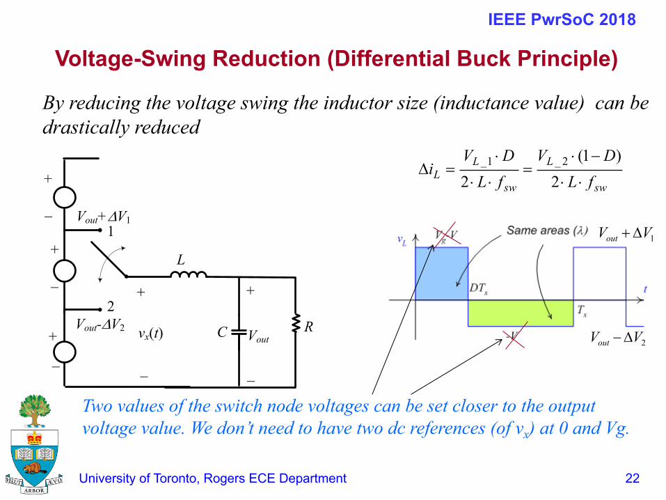
Voltage-Swing Reduction (Differential Buck Principle)
sw
L
sw
LL fL
DVfLDV
i××
-×=
××
×=D
2)1(
22_1_
Two values of the switch node voltages can be set closer to the output voltage value. We don’t need to have two dc references (of vx) at 0 and Vg.
L
Vout
+
_
C R
+
_
vx(t)
Vout+DV1
Vout-DV2
1
2
+
_
_
_
++
1VVout D+
2VVout D-
IEEE PwrSoC 2018
By reducing the voltage swing the inductor size (inductance value) can be drastically reduced
Nov. 25th -26th, 2014, Moscow
23University of Toronto, Rogers ECE Department
IEEE COMPEL 2016
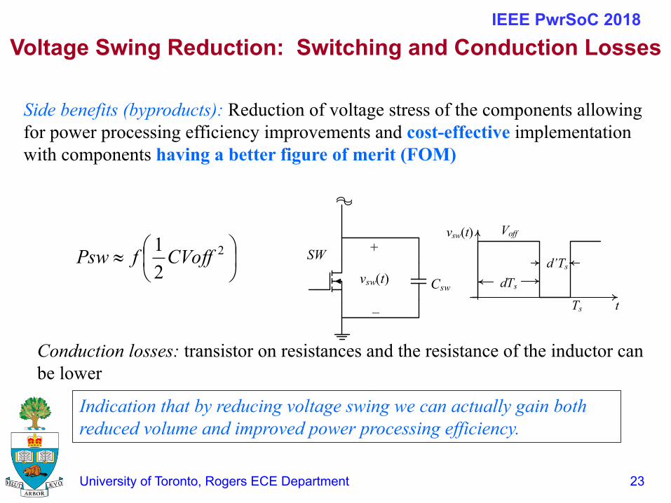
Voltage Swing Reduction: Switching and Conduction Losses
vsw(t)
+
_Csw
SWvsw(t)
dTsd’Ts
Voff
Ts t
Side benefits (byproducts): Reduction of voltage stress of the components allowing for power processing efficiency improvements and cost-effective implementation with components having a better figure of merit (FOM)
÷øö
çèæ» 2
21CVofffPsw
Conduction losses: transistor on resistances and the resistance of the inductor can be lower
Indication that by reducing voltage swing we can actually gain both reduced volume and improved power processing efficiency.
IEEE PwrSoC 2018
Nov. 25th -26th, 2014, Moscow
24University of Toronto, Rogers ECE Department
IEEE COMPEL 2016
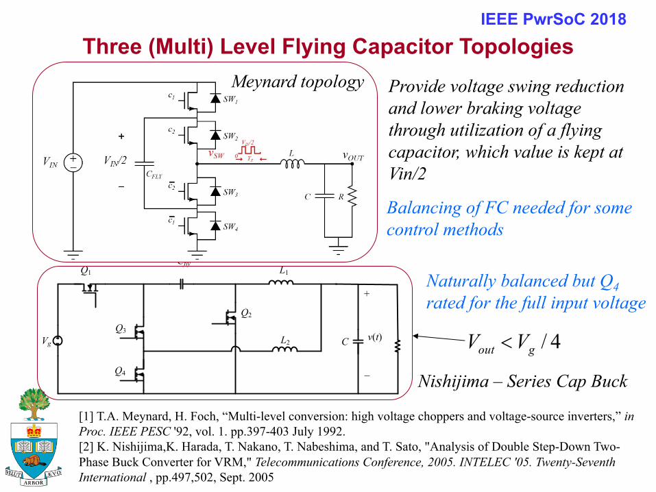
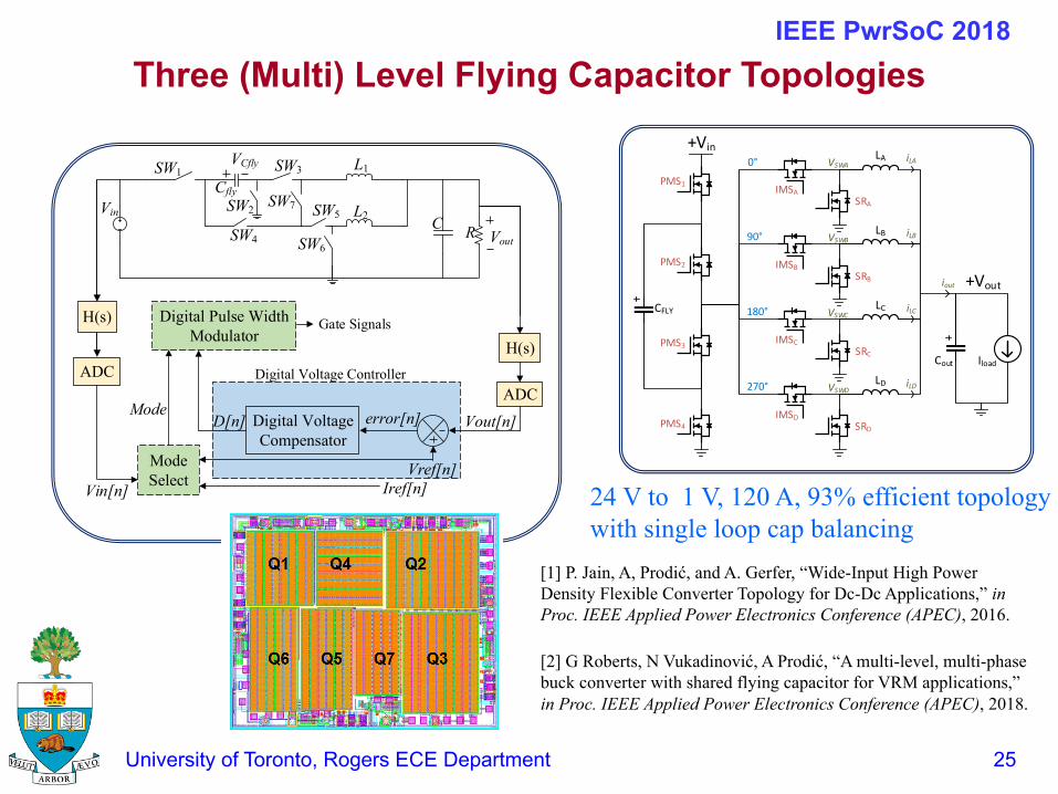
Three (Multi) Level Flying Capacitor Topologies
Vg
L1
v(t)
+_
C
CflyQ1
Q2Q3
Q4
L2
[1] T.A. Meynard, H. Foch, “Multi-level conversion: high voltage choppers and voltage-source inverters,” in Proc. IEEE PESC '92, vol. 1. pp.397-403 July 1992.[2] K. Nishijima,K. Harada, T. Nakano, T. Nabeshima, and T. Sato, "Analysis of Double Step-Down Two-Phase Buck Converter for VRM," Telecommunications Conference, 2005. INTELEC '05. Twenty-Seventh International , pp.497,502, Sept. 2005
Provide voltage swing reduction and lower braking voltage through utilization of a flying capacitor, which value is kept at Vin/2
Meynard topology
4/gout VV <
Nishijima – Series Cap Buck
IEEE PwrSoC 2018
Balancing of FC needed for some control methods
Naturally balanced but Q4rated for the full input voltage
Nov. 25th -26th, 2014, Moscow
25University of Toronto, Rogers ECE Department
IEEE COMPEL 2016
VinVout
SW1 SW3
C
CflyL1
RL2
SW4
SW2 SW5
SW6
SW7
H(s)
ADCDigital Voltage Controller
Vout[n]
Vref[n]
Digital Voltage Compensator
Digital Pulse Width Modulator
Gate Signals
D[n]
VCfly
Iref[n]
Mode Select
H(s)
ADC
Vin[n]
Mode error[n]
[1] P. Jain, A, Prodić, and A. Gerfer, “Wide-Input High Power Density Flexible Converter Topology for Dc-Dc Applications,” in Proc. IEEE Applied Power Electronics Conference (APEC), 2016.
[2] G Roberts, N Vukadinović, A Prodić, “A multi-level, multi-phase buck converter with shared flying capacitor for VRM applications,”in Proc. IEEE Applied Power Electronics Conference (APEC), 2018.
CFLY
Cout
+ViniLA
iLB
iLC
iLD
iout
VSWA
VSWB
VSWC
VSWD
0°
90°
180°
270°
PMS1
PMS2
PMS3
PMS4
IMSA
IMSB
IMSC
IMSD
SRA
SRB
SRC
SRD
LA
LB
LC
LD
Iload
+Vout
IEEE PwrSoC 2018Three (Multi) Level Flying Capacitor Topologies
24 V to 1 V, 120 A, 93% efficient topologywith single loop cap balancing
Nov. 25th -26th, 2014, Moscow
26University of Toronto, Rogers ECE Department
IEEE COMPEL 2016
Control of Hybrid Multi-Level FC Topologies
IEEE PwrSoC 2018
Nov. 25th -26th, 2014, Moscow
27University of Toronto, Rogers ECE Department
IEEE COMPEL 2016IEEE COMPEL 2016
Reasons for not Using FC ConvertersIEEE PwrSoC 2018
§ Flying capacitor instability problems in:
§ PWM voltage mode
§ Peak current programmed mode
§ Average current programmed mode
§ Challenges of operating at light loads
§ Start-up and input load transient challenges [1]
§ Different failure mechanisms compared to conventional structures
§ Not fully understood/explored system dynamics
§ Pin count (pad ring) increase for IC implementation
§ Losses of flying capacitor esr…
(Sceptics Guide on Trashing FC Converters Idea)
[1] M. Halamicek, T. Moiannou, N. Vukadinović, and A. Prodić “Capacitive divider based passive start-up methods for flying capacitor step-down dc-dc converter topologies,” in Proc. IEEE ECCE-Asia/IPEC, 2018.
Nov. 25th -26th, 2014, Moscow
28University of Toronto, Rogers ECE Department
IEEE COMPEL 2016IEEE COMPEL 2016
There are Some Good Control News as WellIEEE PwrSoC 2018
§ Further improvement of transient response performance (further reduction of the output capacitor) J
§ Opening possibilities for on-line efficiency improvement J
§ Create opportunities for new (digital) control methods to make them even smaller and/or more efficient J
Potential benefits are just too good to quit on the idea and, again, the existing solutions just cannot keep on with some emerging requirements (increased conversion ratio and power ratings)
Nov. 25th -26th, 2014, Moscow
29University of Toronto, Rogers ECE Department
IEEE COMPEL 2016
PWM Voltage Mode Flying Capacitor Balancing Challenges and Solutions
IEEE PwrSoC 2018
Nov. 25th -26th, 2014, Moscow
30University of Toronto, Rogers ECE Department
IEEE COMPEL 2016
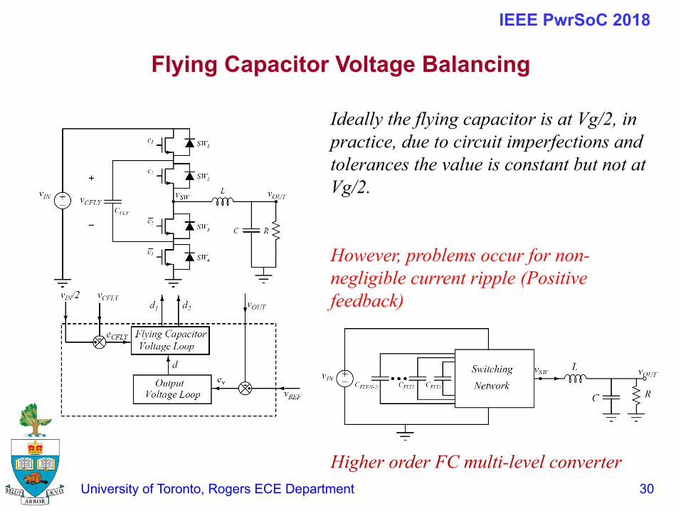
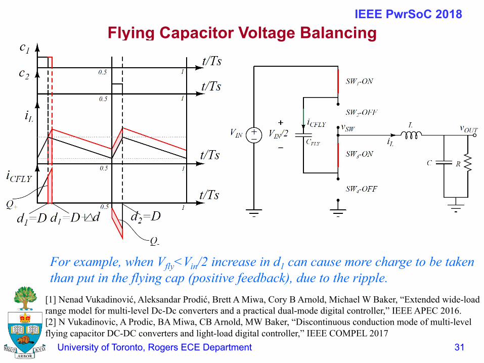
Flying Capacitor Voltage Balancing
Ideally the flying capacitor is at Vg/2, in practice, due to circuit imperfections and tolerances the value is constant but not at Vg/2.
However, problems occur for non-negligible current ripple (Positive feedback)
Higher order FC multi-level converter
IEEE PwrSoC 2018
Nov. 25th -26th, 2014, Moscow
31University of Toronto, Rogers ECE Department
IEEE COMPEL 2016
Flying Capacitor Voltage Balancing
For example, when Vfly<Vin/2 increase in d1 can cause more charge to be taken than put in the flying cap (positive feedback), due to the ripple.
IEEE PwrSoC 2018
[1] Nenad Vukadinović, Aleksandar Prodić, Brett A Miwa, Cory B Arnold, Michael W Baker, “Extended wide-load range model for multi-level Dc-Dc converters and a practical dual-mode digital controller,” IEEE APEC 2016.[2] N Vukadinovic, A Prodic, BA Miwa, CB Arnold, MW Baker, “Discontinuous conduction mode of multi-level flying capacitor DC-DC converters and light-load digital controller,” IEEE COMPEL 2017
Nov. 25th -26th, 2014, Moscow
32University of Toronto, Rogers ECE Department
IEEE COMPEL 2016
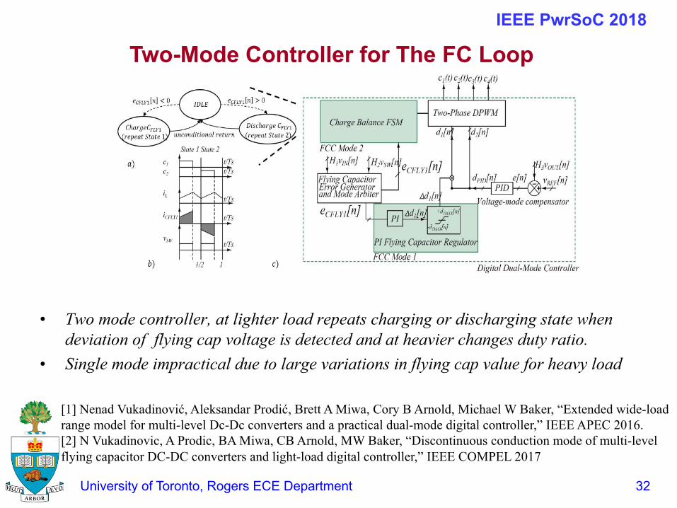
Two-Mode Controller for The FC Loop
• Two mode controller, at lighter load repeats charging or discharging state when deviation of flying cap voltage is detected and at heavier changes duty ratio.
• Single mode impractical due to large variations in flying cap value for heavy load
IEEE PwrSoC 2018
[1] Nenad Vukadinović, Aleksandar Prodić, Brett A Miwa, Cory B Arnold, Michael W Baker, “Extended wide-load range model for multi-level Dc-Dc converters and a practical dual-mode digital controller,” IEEE APEC 2016.[2] N Vukadinovic, A Prodic, BA Miwa, CB Arnold, MW Baker, “Discontinuous conduction mode of multi-level flying capacitor DC-DC converters and light-load digital controller,” IEEE COMPEL 2017
Nov. 25th -26th, 2014, Moscow
33University of Toronto, Rogers ECE Department
IEEE COMPEL 2016
CPM Control Challenges
And Solutions
IEEE PwrSoC 2018
Nov. 25th -26th, 2014, Moscow
34University of Toronto, Rogers ECE Department
IEEE COMPEL 2016IEEE COMPEL 2016
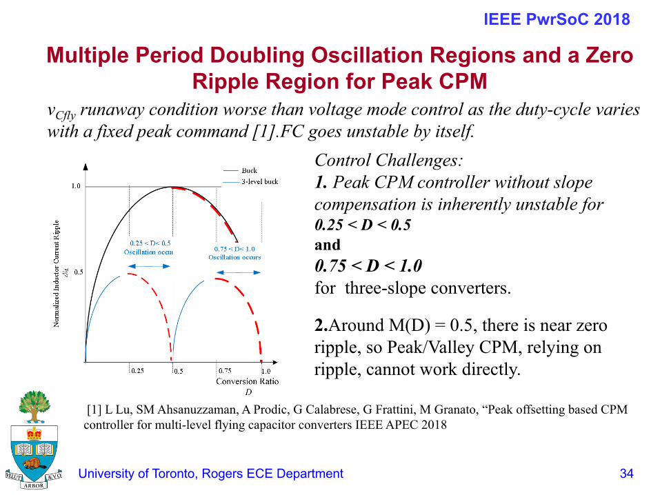
Control Challenges:1. Peak CPM controller without slope compensation is inherently unstable for 0.25 < D < 0.5and 0.75 < D < 1.0for three-slope converters.
2.Around M(D) = 0.5, there is near zero ripple, so Peak/Valley CPM, relying on ripple, cannot work directly.
Multiple Period Doubling Oscillation Regions and a Zero Ripple Region for Peak CPM
IEEE PwrSoC 2018
[1] L Lu, SM Ahsanuzzaman, A Prodic, G Calabrese, G Frattini, M Granato, “Peak offsetting based CPM controller for multi-level flying capacitor converters IEEE APEC 2018
vCfly runaway condition worse than voltage mode control as the duty-cycle varies with a fixed peak command [1].FC goes unstable by itself.
Nov. 25th -26th, 2014, Moscow
35University of Toronto, Rogers ECE Department
IEEE COMPEL 2016IEEE COMPEL 2016
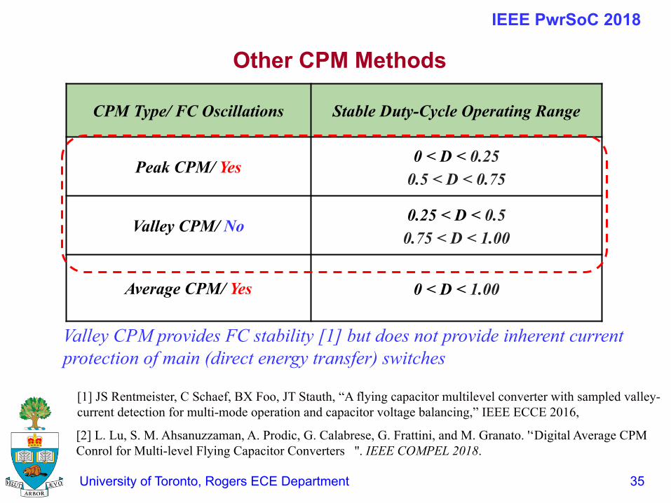
CPM Type/ FC Oscillations Stable Duty-Cycle Operating Range
Peak CPM/ Yes 0 < D < 0.25 0.5 < D < 0.75
Valley CPM/ No 0.25 < D < 0.50.75 < D < 1.00
Average CPM/ Yes 0 < D < 1.00
Other CPM Methods
Valley CPM provides FC stability [1] but does not provide inherent current protection of main (direct energy transfer) switches
IEEE PwrSoC 2018
[1] JS Rentmeister, C Schaef, BX Foo, JT Stauth, “A flying capacitor multilevel converter with sampled valley-current detection for multi-mode operation and capacitor voltage balancing,” IEEE ECCE 2016,
[2] L. Lu, S. M. Ahsanuzzaman, A. Prodic, G. Calabrese, G. Frattini, and M. Granato. '‘Digital Average CPM Conrol for Multi-level Flying Capacitor Converters ''. IEEE COMPEL 2018.
Nov. 25th -26th, 2014, Moscow
36University of Toronto, Rogers ECE Department
IEEE COMPEL 2016IEEE COMPEL 2016
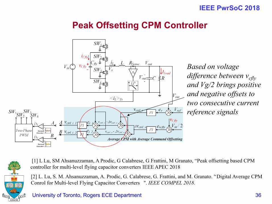
Peak Offsetting CPM Controller
Based on voltage difference between vcflyand Vg/2 brings positive and negative offsets to two consecutive current reference signals
IEEE PwrSoC 2018
[2] L. Lu, S. M. Ahsanuzzaman, A. Prodic, G. Calabrese, G. Frattini, and M. Granato. '‘Digital Average CPM Conrol for Multi-level Flying Capacitor Converters ''. IEEE COMPEL 2018.
[1] L Lu, SM Ahsanuzzaman, A Prodic, G Calabrese, G Frattini, M Granato, “Peak offsetting based CPM controller for multi-level flying capacitor converters IEEE APEC 2018
Nov. 25th -26th, 2014, Moscow
37University of Toronto, Rogers ECE Department
IEEE COMPEL 2016IEEE COMPEL 2016
v_OUT
v_CFLY
i_L
v_X
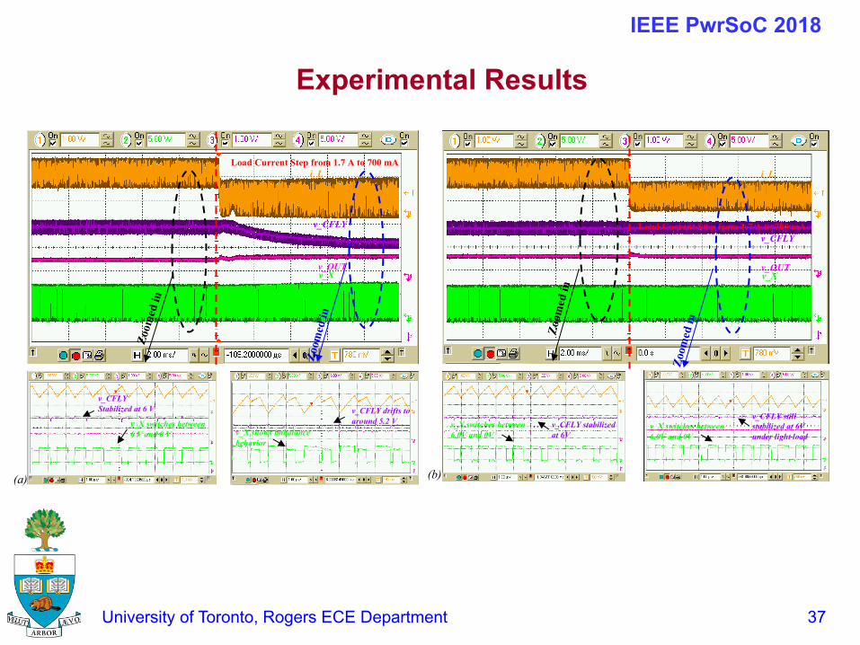
Load Current Step from 1.7 A to 700 mA
v_CFLY drifts to around 5.2 V
v_X shows imbalance behavior
Load Current Step from 1.7 A to 700 mA
v_X switches between 6.0V and 0V
v_CFLY still stabilized at 6V under light load
i_L
v_CFLY
v_OUTv_X
v_X switches between 6 V and 0 V
v_CFLY Stabilized at 6 V
(a)
v_CFLY stabilized at 6V
v_X switches between 6.0V and 0V
(b)
Experimental Results
IEEE PwrSoC 2018
Nov. 25th -26th, 2014, Moscow
38University of Toronto, Rogers ECE Department
IEEE COMPEL 2016
Failure Mechanisms: Voltage Spikes at Zero Ripple Operating Points
IEEE PwrSoC 2018
Nov. 25th -26th, 2014, Moscow
39University of Toronto, Rogers ECE Department
IEEE COMPEL 2016IEEE COMPEL 2016
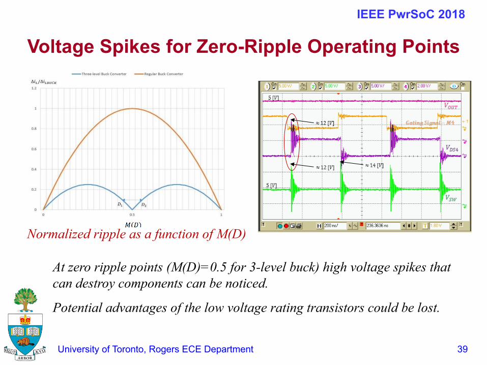
Voltage Spikes for Zero-Ripple Operating Points
At zero ripple points (M(D)=0.5 for 3-level buck) high voltage spikes that can destroy components can be noticed.
Potential advantages of the low voltage rating transistors could be lost.
Normalized ripple as a function of M(D)
IEEE PwrSoC 2018
Nov. 25th -26th, 2014, Moscow
40University of Toronto, Rogers ECE Department
IEEE COMPEL 2016IEEE COMPEL 2016
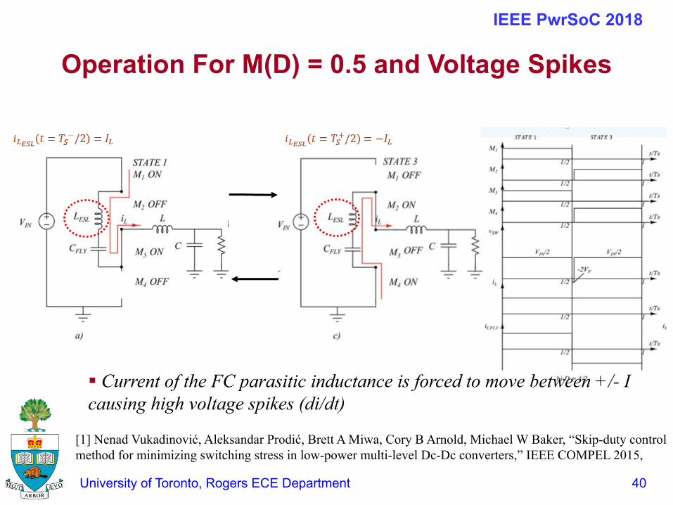
Operation For M(D) = 0.5 and Voltage Spikes
§ Current of the FC parasitic inductance is forced to move between +/- I causing high voltage spikes (di/dt)
[1] Nenad Vukadinović, Aleksandar Prodić, Brett A Miwa, Cory B Arnold, Michael W Baker, “Skip-duty control method for minimizing switching stress in low-power multi-level Dc-Dc converters,” IEEE COMPEL 2015,
IEEE PwrSoC 2018
Nov. 25th -26th, 2014, Moscow
41University of Toronto, Rogers ECE Department
IEEE COMPEL 2016IEEE COMPEL 2016
Elimination Through Skip-Duty & Sequencing
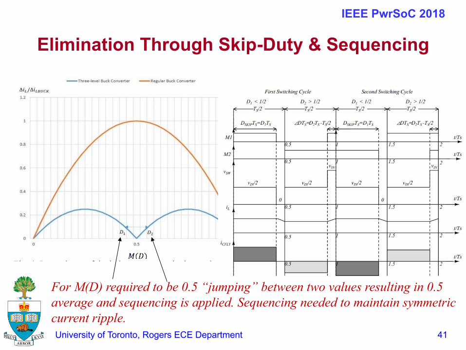
For M(D) required to be 0.5 “jumping” between two values resulting in 0.5 average and sequencing is applied. Sequencing needed to maintain symmetric current ripple.
IEEE PwrSoC 2018
Nov. 25th -26th, 2014, Moscow
42University of Toronto, Rogers ECE Department
IEEE COMPEL 2016IEEE COMPEL 2016
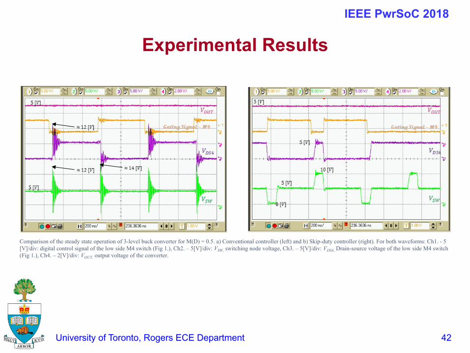
Comparison of the steady state operation of 3-level buck converter for M(D) = 0.5. a) Conventional controller (left) and b) Skip-duty controller (right). For both waveforms: Ch1. - 5 [V]/div: digital control signal of the low side M4 switch (Fig 1.), Ch2. – 5[V]/div: VSW, switching node voltage, Ch3. – 5[V]/div: VDS4, Drain-source voltage of the low side M4 switch (Fig 1.), Ch4. – 2[V]/div: VOUT, output voltage of the converter.
Experimental Results
IEEE PwrSoC 2018
Nov. 25th -26th, 2014, Moscow
43University of Toronto, Rogers ECE Department
IEEE COMPEL 2016
Some Good News: Transient Response Improvement and On-Line Efficiency Optimization
IEEE PwrSoC 2018
Nov. 25th -26th, 2014, Moscow
44University of Toronto, Rogers ECE Department
IEEE COMPEL 2016IEEE COMPEL 2016
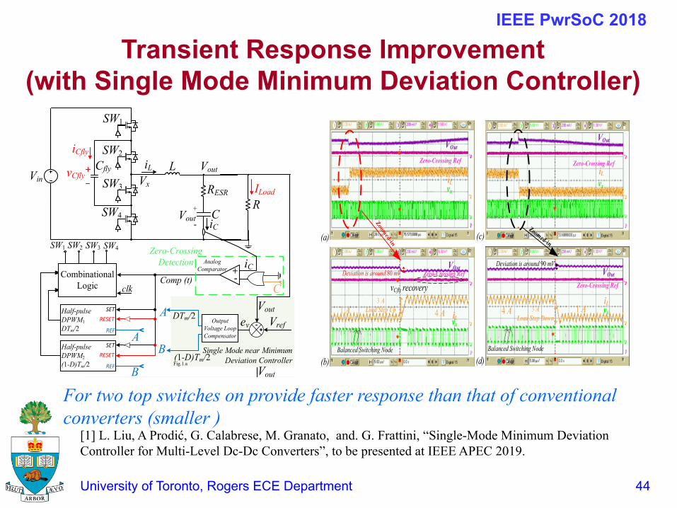
Transient Response Improvement (with Single Mode Minimum Deviation Controller)
For two top switches on provide faster response than that of conventional converters (smaller )
IEEE PwrSoC 2018
Cfly LvCfly Vx
+
-C
RVout
Vout
SW1
SW2
SW3
SW4
Vin
iCfly
ILoad
iL
RESR
iC
iC Analog
Comparator +-
Zero-Crossing Detection
Vref evA
B
DTm/2
(1-D)Tm/2
Half-pulse DPWM1 DTm/2
SET
REF
RESET
Half-pulse DPWM2 (1-D)Tm/2
SET
REF
RESET
Vout
Comp (t)
Output Voltage Loop Compensator
vCflyVin / 2 evcfly
ΔDTm
Vref ev
Vout
Fig.1.a with Duty-cycle Adjustment
PI
DTm/2(1-D)Tm/2
D1Tm/2
D2Tm/20First Half
1
A
B
A
B
vCflyVin / 2 evcfly
Δi_Adjustment
Vref ev
Vout
DTm/2(1-D)Tm/2
0First Half
1
AB
+Δi_Adjustment
-Δi_AdjustmentC
CCombinational
Logic clk
SW1 SW2 SW3 SW4
Fig.1.a with Zero-Crossing Adjustment
Single Mode near Minimum Deviation Controller Fig.1.a
Fig.1.b
Fig.1.c
Output Voltage Loop Compensator
FC Voltage Loop
Compensator
Output Voltage Loop Compensator
FC Voltage Loop
Compensator
VOut
Zero-Crossing Ref
iLvx
VOut
iLvx
Zero-Crossing Ref
VOut
Zero-Crossing RefiL
vx
VOut
Zero-Crossing Ref
iLvx
Deviation is around 80 mVDeviation is around 90 mV
1 A 4 A3 A
Load Step Up 4 A 1 A3 A Load Step Down
vCfly recovery
(a) (c)
(b) (d)Balanced Switching Node Balanced Switching Node
[1] L. Liu, A Prodić, G. Calabrese, M. Granato, and. G. Frattini, “Single-Mode Minimum Deviation Controller for Multi-Level Dc-Dc Converters”, to be presented at IEEE APEC 2019.
Nov. 25th -26th, 2014, Moscow
45University of Toronto, Rogers ECE Department
IEEE COMPEL 2016IEEE COMPEL 2016
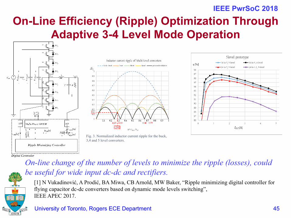
On-Line Efficiency (Ripple) Optimization Through Adaptive 3-4 Level Mode Operation
Fig. 3. Normalized inductor current ripple for the buck, 3,4 and 5 level converters.
On-line change of the number of levels to minimize the ripple (losses), could be useful for wide input dc-dc and rectifiers.
IEEE PwrSoC 2018
[1] N Vukadinović, A Prodić, BA Miwa, CB Arnold, MW Baker, “Ripple minimizing digital controller for flying capacitor dc-dc converters based on dynamic mode levels switching”,IEEE APEC 2017.
Nov. 25th -26th, 2014, Moscow
46University of Toronto, Rogers ECE Department
IEEE COMPEL 2016IEEE COMPEL 2016
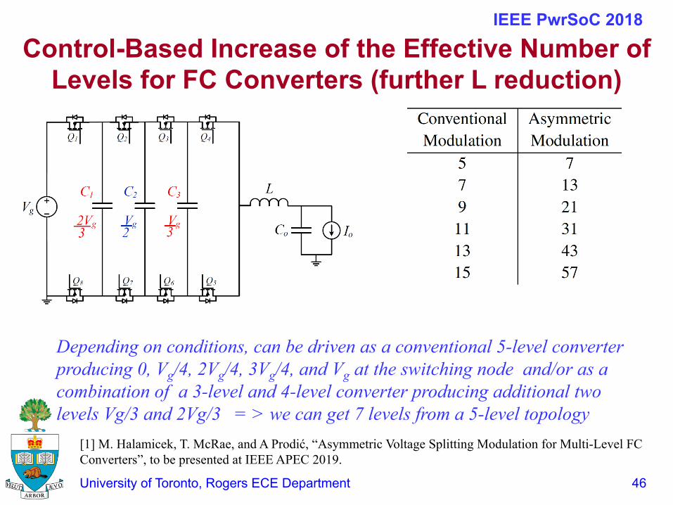
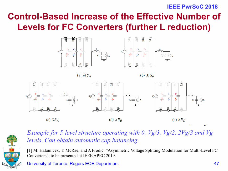
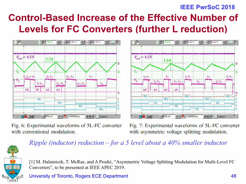
Control-Based Increase of the Effective Number of Levels for FC Converters (further L reduction)
IEEE PwrSoC 2018
[1] M. Halamicek, T. McRae, and A Prodić, “Asymmetric Voltage Splitting Modulation for Multi-Level FC Converters”, to be presented at IEEE APEC 2019.
Depending on conditions, can be driven as a conventional 5-level converter producing 0, Vg/4, 2Vg/4, 3Vg/4, and Vg at the switching node and/or as a combination of a 3-level and 4-level converter producing additional two levels Vg/3 and 2Vg/3 = > we can get 7 levels from a 5-level topology
Nov. 25th -26th, 2014, Moscow
47University of Toronto, Rogers ECE Department
IEEE COMPEL 2016IEEE COMPEL 2016
Control-Based Increase of the Effective Number of Levels for FC Converters (further L reduction)
IEEE PwrSoC 2018
[1] M. Halamicek, T. McRae, and A Prodić, “Asymmetric Voltage Splitting Modulation for Multi-Level FC Converters”, to be presented at IEEE APEC 2019.
Example for 5-level structure operating with 0, Vg/3, Vg/2, 2Vg/3 and Vg levels. Can obtain automatic cap balancing.
Nov. 25th -26th, 2014, Moscow
48University of Toronto, Rogers ECE Department
IEEE COMPEL 2016IEEE COMPEL 2016
Control-Based Increase of the Effective Number of Levels for FC Converters (further L reduction)
IEEE PwrSoC 2018
[1] M. Halamicek, T. McRae, and A Prodić, “Asymmetric Voltage Splitting Modulation for Multi-Level FC Converters”, to be presented at IEEE APEC 2019.
Ripple (inductor) reduction – for a 5 level about a 40% smaller inductor
Nov. 25th -26th, 2014, Moscow
49University of Toronto, Rogers ECE Department
IEEE COMPEL 2016IEEE COMPEL 2016
Conclusions and Future Challenges
IEEE PwrSoC 2018
§ By utilizing reduced voltage and current swing principles new control and topological solutions can be found
§ Single-mode minimum deviation controller provides virtually minimum voltage deviation resulting in the minimum size of output cap for direct energy transfer converters
§ FC converter topologies bring advantages of lower size, improved efficiency (at the same time) with potentially lower cost of implementation, but also bring (solvable) challenges related to their control
§ FC converters also open possibility for developing new control methods that could significantly improve their efficiency and further reduce the size
Nov. 25th -26th, 2014, Moscow
50University of Toronto, Rogers ECE Department
IEEE COMPEL 2016IEEE COMPEL 2016
Thank You.
IEEE PwrSoC 2018