Embed Size (px)
Citation preview

High Performance Direct-Current Generator Based on Dynamic
PN Junctions
Yanghua Lu1, Sirui Feng1, Zhenzhen Hao1, Runjiang Shen1 and Shisheng Lin1,2,*
1: College of Microelectronics, College of Information Science and Electronic
Engineering, Zhejiang University, Hangzhou, 310027, China
2: State Key Laboratory of Modern Optical Instrumentation, Zhejiang University,
Hangzhou, 310027, China
*Corresponding author. Tel: +86-0571-87951555
Email: [email protected].
Abstract
After the electromagnetic generator, searching for novel electric generators without
strong magnetic field is highly demanded. The generator without strong magnetic
field calls for a physical picture distinct from the traditional generators. As the
counterpart of the static PN junction has been widely used in the integrated circuits,
we develop an electric generator named “dynamic PN generator” with a high current
density and voltage output, which converts mechanical energy into electricity by
sliding two semiconductors with different Fermi level. A dynamic N-GaAs/SiO2/P-Si
generator with the open-circuit voltage of 3.1 V and short-circuit density of 1.0 A/m2
have been achieved. The physical mechanism of the dynamic PN generator is
proposed based on the built-in electric field bounding back diffusing carriers in
dynamic PN junctions, which breaks the equilibrium between drift and diffusion
current in the PN junction. Moreover, the dynamic MoS2/AlN/Si generator with the
open-circuit voltage of 5.1 V and short-circuit density of 112 A/m2 (11.2 mA/cm2)
have also been achieved, which can effectively output a direct-current and light up a
blue light-emitting diode directly. This dynamic MoS2/AlN/Si generator can
continuously work for hours without obvious degradation, demonstrating its unique
mechanism and potential applications in many fields where the mechanical energy is
available.
Main
The understanding of electron movements advances the information society and
satisfying the requirements of electrical energy for human society. Michael Faraday is
well known for the discovery of electromagnetic induction, who revealed the
connection between magnetism and electricity in the year of 18311. In
electromagnetic generator, the electricity was generated when an electrical conductor
passes through a magnetic field. Before that, electric generators were mainly referred
to electrostatic generators under the operation principles of electrostatic induction and
triboelectric effect2. Recently, the piezoelectric and triboelectric nanogenerators3,4
attract many attentions, which could get electricity from the blue environmental
energy such as mechanical and vibrating energy5,6. According to the proposed
mechanism, the triboelectricity utilizes the displacement current in the Maxwell
equation, which cannot flow freely through the insulating dielectric materials, may
limiting its current output density7. On the other hand, solar cell works under the light
illumination environments has although developed many novel structures8-10. It is
imperative to search for a novel electric generator with high current density, which is

the bottleneck of the current generators without high magnetic field under dark
environments11-16.
Since the invention of PN junction in 1940s17, many applications have been
explored such as the integrated circuits18. However, the dynamic PN junction has been
rarely explored because most applications are focused on the static PN structure for
the development of information society19. Recently, we have independently reported
the dynamic Schottky diode as a direct current generator20, and proposed the physical
picture different from the triboelectricity21,22. However, as the Fermi level difference
between metal and semiconductor is rather limited, which leads to a voltage output
less than 1.0 V. The PN junction is totally different from Schottky diode as PN
junction is minority carrier device while Schottky diode is majority carrier device, and
the built-in voltage of the PN junction can be much larger than the Schottky diode as
the Fermi level difference between N-type and P-type semiconductor can be several
times of that of metal and semiconductor. Herein, we have demonstrated a high
current density novel direct-current (d.c.) generator based on the dynamic PN junction,
named as “dynamic PN generator”, through sliding one semiconductor over another
semiconductor with different Femi level, which can light up the light emitting diodes
(LEDs) without any external rectifying circuits. The connected dynamic PN junction
in series can output voltage larger than 9.0 V. The work mechanism is based on the
built-in electric field separation of the otherwise diffused carriers as a result of the
destruction and establishment of the depletion layer in dynamic PN junctions, which
breaks the equilibrium between the drift and diffusion current, leading to an electricity

output whose mechanism is different from other types of electric generators1-4.
Typically, a dynamic GaAs/Si junction can convert the mechanical energy into
electricity, whose open-circuit voltage (Voc) reaches 0.7 V and short-circuit density
(Jsc) reaches 1.8 A/m2. Both the Voc and Jsc are the peak value of voltage and current
output. Furthermore, compared with the semiconductor-semiconductor dynamic PN
generator, the semiconductor-insulator-semiconductor structure based dynamic PN
generator outputs higher voltage attributed to the interface passivation and insulator
bounding effect under the localized built-in electric field23,24, whose Voc can reach 3.1
V and Jsc can reach 1.0 A/m2 for the case of GaAs/SiO2/Si heterojunction. Moreover,
a dynamic MoS2/AlN/Si generator with Jsc of 112 A/m2 and Voc of 5.1 V has been
achieved. The current density of 112 A/m2 is orders of magnitude higher than
triboelectric nanogenerators (~103 times)7,25,26 and piezoelectric nanogenerators (~104
times)7,27,28, which can be further enhanced through optimizing the PN junction
interface and structure26,29. Without external rectifying circuit, this dynamic PN
generator has the unique advantage of ultrahigh current density and direct-current
output ability20-22. This dynamic PN generator can be connected in series or in parallel,
which can effectively increase the output voltage or current. Two and three dynamic
P-Si/N-GaAs generators in series can effectively output a voltage of 6.1 V and 9.0 V,
which can light up a blue light-emitting diode (LED) directly. Especially, the dynamic
P-Si/AlN/MoS2 generator does not show obvious degradation after 60 min of running,
confirming its mechanism is different from the triboelectricity and proving the
potential applications of the dynamic PN generator30,31 .

As a representative dynamic PN generator, the schematic structure of the
dynamic GaAs/Si generator is illustrated in Figure 1a. The N-type GaAs wafer was
pressed on the P-type Si substrate compactly with a 6N force, which showed typical
rectification behavior with a low leakage current density of 1.5 µA/cm2 under the bias
voltage of -3 V (Figure 1b). The work function of N-type GaAs and P-type Si used
here is 4.10 eV and 5.12 eV (as shown in the Supplementary Note 1), respectively.
Accordingly, the work function of N-GaAs is smaller than P-Si, thus a built-in electric
field will be formed between the N-GaAs and P-Si substrate. Primarily, the N-type
GaAs was dragged along the surface of the P-type Si and a maximal Voc up to 0.7 V
was observed, which is independent on the working area. The dynamic P-Si/N-Si and
P-Si/N-GaN junction can also output voltage signal as well as P-Si/N-GaAs junction,
among which the Voc of P-Si/N-GaAs junction is the highest, which is 7 times of
dynamic P-Si/N-Si generator (Figure 1c). The Fermi level of N-Si and N-GaN are
about 4.28 eV and 4.35 eV (as shown in the Supplementary Note 1), so the generated
voltage direction of P-Si/N-Si and P-Si/N-GaN generator is same as the P-Si/N-GaAs
generator,confirming the importance of Fermi level (some other semiconductors are
also explored in the Supplementary Figure 1). It is noteworthy that only noise
electricity can be produced when sliding one piece of P-type Si over another P-type Si
with same Fermi level (Supplementary Figure 2), indicating the important role of
Fermi level difference and the built-in field. Figure 1d shows that the current output is
positively proportional to the work area, indicating the current output can be
improved by enlarging the work area. For a GaAs/Si dynamic PN generator with a

working area of 1.0 mm2 (2cm × 0.05mm), a maximal peak short-circuit current (Isc)
up to 1.8 µA was observed primitively, which was positive related to the movement
speed within limits (Supplementary Figure 3). The Jsc up to 1.8 A/m2 can be achieved,
which is orders of magnitudes higher than the reported polymer-based triboelectric
nanogenerators (in the order of 10-1 A/m2)7,25,26 and piezoelectric generators (in the
order of 10-2 A/m2)7,27,28. Furthermore, the relationship between the Voc/Isc and the
force exerted on device is explored and it is found that the force of 6N is the optimal
choice (Figure 1e), where the N-GaAs and P-Si can have the best rectification
characteristic (as shown in J-V curves of the P-Si/N-GaAs junction under different
forces in Supplementary Figure 4 and NIF in Supplementary Note 2). The 3D diagram
for converting mechanical energy into electrical energy by the dynamic PN junction is
shown in Figure 1f, which can work in the linearly reciprocating mode or circularly
rotating mode. Figure 1g and Figure 1h show the Isc of the generator in linearly
reciprocating mode and circularly rotating mode, respectively. It can be seen that the
linear reciprocating mode outputs a pulsed current, which is caused by the inevitable
acceleration and deceleration of the GaAs wafer motion. In contrast, when the GaAs
wafer is continuously and evenly slide under the circularly rotating mode, it outputs a
sustained direct current. The continuous d.c. output of our dynamic P-Si/N-GaAs
generator indicates its unique physical mechanism different from the contact mode
generator of PN generator or triboelectric generators.

Figure 1. Experimental designs and results of the dynamic PN generator. a) The
schematic illustration of the dynamic P-Si/N-GaAs generator. b) The J-V curve
of the static P-Si/N-GaAs junction with a 6N force. The contact area is 1.0 mm2. c)
The Voc of dynamic P-Si/N-Si, P-Si/N-GaN, P-Si/N-GaAs generator with a speed
of 6cm/s and a 6N force. d) The Isc of dynamic P-Si/N-GaAs generator with a 6N
force, a speed of 6 cm/s and the work area of 0.15, 0.25, 0.5, 0.75, 1.0 mm2. e) The
Voc and Isc of dynamic P-Si/N-GaAs generator with different force exerted on the
junction in a speed of 6 cm/s. f) Experimental design and 3D diagram for
converting mechanical energy into electrical energy by a dynamic PN junction.
The inset shows the linearly reciprocating and circularly rotating modes of the
generator, respectively. g) and h) show the Isc of dynamic P-Si/N-GaAs generator
under the linearly reciprocating mode and circularly rotating mode with a 6N
force and a speed of 6 cm/s, respectively.

As schematically shown in Figure 2, when we move the PN junction in time
pieces, the destruction of the PN junction at the rear part and establishment at the
front part will happen subsequently. We name this junction ‘the dynamic PN junction’.
The destruction of the PN junction at the rear part inhibits the diffusion paths for the
diffusing electrons and holes, which is necessary for balancing the drift current. Those
otherwise diffused carriers are bound back and accelerated by the built-in field. As the
P-type side contacts with N-type side at the front part, the drift current will balance
with the diffusion current very soon. As time passes in a series of pieces, more
electrons and holes are bound back the N-type side and P-type side, respectively,
leading a net current output and building a voltage output. Figure 2a shows the
schematic illustration of the P-Si/N-GaAs interface. Actually, for the P-Si/N-GaAs
junction, the drift-diffusion current equation can be described as below32:
𝐽! = 𝐽!!"#$% + 𝐽!
!"## = 𝑞𝑛𝑢!E+ 𝑞𝐷!∇𝑛 (1)
𝐽! = 𝐽!!"#$% + 𝐽!
!"## = 𝑞𝑝𝑢!E− 𝑞𝐷!∇𝑝 (2)
where Jn, Jp, µn, µp, Dn, Dp are the electron/hole current density, the electron/hole
mobility and the electron/hole diffusion coefficient of GaAs and Si, respectively. E is
the built-in field, q is the elementary charge, n and p are the position dependent
electron/hole density in GaAs and Si, respectively. When the GaAs wafer moves
along the Si substrate, there is a dynamic process of disappearance of the depletion
layer in the rear end and the re-establishment of the depletion layer in the front end. In
macro scale, the effective working area of the dynamic PN junction is assumed as the
contact area of the GaAs wafer and Si substrate during the movement. According to

equation (1) and (2), the current density of GaAs/Si junction is consisted of Jdiff and
Jdrift. However, the dynamic process of the generation and disappearance of the
depletion layer in dynamic GaAs/Si junction will break up the static carrier
distribution equilibrium and bound back the electrons or holes which are diffusing
across the depletion layer. The bounding back electrons and holes under the built-in
field lead to increase of Jdrift and decrease of Jdiff, breaking up the equilibrium of
drift-diffusion current in the static PN junction, which is the origin of the output
current generated in dynamic PN junction. The rectification characteristic of the
dynamic N-GaAs/P-Si junction from -5V to 5V was measured and shown in Figure
2b, where the oscillation of the J-V curve as voltage increases. The oscillation of the
current value indicates there are destruction and re-establishment of the depletion
layer in the dynamic PN junction, which is in agreement with the previous proposed
physical picture. The detailed transportation of the bound back electron and hole are
shown in Figure 2c, where also includes the band gap alignment between P-Si and
N-GaAs. The built-in field point to P-Si as a result of electron diffusion from N-GaAs
to P-Si. When the N-GaAs wafer is dragged on P-Si, the diffusing electrons and holes
in the rear part has no way to diffuse into P-Si and N-GaAs, respectively. Thus, under
the effect of built-in field, the otherwise diffused electron and holes in the rear part are
bound back to the N-GaAs and P-Si, respectively, breaking up the equilibrium of
drift-diffusion current and forming electrical output. So the built-in electric field and
the barrier height of the PN junction must play a crucial role. The temperature
difference of semiconductors before and after the friction is very limited
(Supplementary Figure 5), which indicates that the heat effect is ignorable for
outputting electrical signal.
To reveal this distinctive current generation mechanism and prove the barrier
height of the PN junction plays a crucial role in our generator, P-type silicon wafers
with different thickness (d) of silicon oxide are used here for further experiments. We
find this dynamic semiconductor-insulator-semiconductor structure generator has
higher voltage output because of the increased barrier height23. As shown in band
diagram of the dynamic N-GaAs/SiO2/P-Si junction (Figure 2d), the barrier height for
bounding back electrons and holes are largely increased as the conduction/valence
bands of SiO2 are much higher/lower than that of GaAs and Si. When we move the
N-GaAs wafer along the SiO2/P-Si substrate, the diffusing electrons and holes can
also be switched back and accelerated by the localized built-in electric field, moving
toward the ohmic contact of N-GaAs and P-Si, respectively. The inserted SiO2 layer
can largely suppress the transfer of electrons and holes, stimulating the bounding back
of diffusing electrons and holes. With the increase of barrier height, more bounding
back electrons and holes accumulate in two semiconductors, increasing the potential
difference as well as the voltage output. Figure 2e indicates that the rectification
characteristic can be largely optimized after inserting the insulating layer, indicating
the increase of the barrier height of the GaAs/Si junction. As shown in Figure 2f, the
Voc and Jsc of the dynamic P-Si/N-GaAs junction with the SiO2 thickness of
0/9/13/20/50/100/200 nm are 0.7/0.9/1.2/1.6/2.2/3.1/4.0 V and
1.8/1.6/1.5/1.4/1.2/1.0/0 A/m2, respectively. With the increase of the thickness of SiO2,

the Jsc decreases faintly to zero for 200 nm thick of SiO2 but the Voc increases
continuously. It is proved that the 200 nm SiO2 is too thick for carriers crossing over
it (Supplementary Figure 6), which lead to a nearly zero current output. The voltage
output can be larger than the Fermi level differences for the cases of thick SiO2, which
should be ascribed to pumped electrons and holes in the N-type and P-type
semiconductor, as the thick SiO2 provides a high and safe barrier for bounding back
the otherwise diffused electrons and holes compared with the case of thin SiO2.
Figure 2. a) The schematic diagram of the dynamic P-Si/N-GaAs generator. b)
The J-V curve of the dynamic P-Si/N-GaAs junction with a 6N force. The contact
area is 1.0 mm2. c) The band diagram and carrier dynamic process of the
dynamic P-Si/N-GaAs generator and d) the dynamic P-Si/SiO2/N-GaAs
generator. e) J-V curves of the dynamic P-Si/N-GaAs generator without SiO2 and
with 20/100 nm SiO2. f) The Voc and Jsc of the dynamic P-Si/N-GaAs generator
with a 6N force, a speed of 6 cm/s and SiO2 thickness of 0/9/13/20/50/100/200 nm.

The work area of the P-Si/N-GaAs junction is 1.0 mm2. Both the Voc and Jsc are
the peak value of voltage and current output.
To explore the potential practical applications, we charged a capacitor C (0.1 µF)
by manually sliding a GaAs wafer on the SiO2/Si substrate. Figure 3a and Figure 3b
show the voltage of charging capacitor in the linearly reciprocating mode and
circularly rotating mode, respectively. It can be seen that the linear reciprocating
mode outputs a pulsed voltage and the circularly rotating mode outputs a continual
voltage as high as 3.1 V under the consistent charging. In addition, the Voc outputs of
the generator in parallel, 2-series and 3-series are 3.1/6.1/9.0 V, indicating the linear
superposition effect of our devices, which can expand its applications (Figure 3c). The
captured optical pictures of this capacitor charging experiment is shown in Figure 3d,
which is consist of a capacitor (0.1 µF), a resistance (47 kΩ), a Keithley 2010 system
and a reset switch. The detailed circuit diagram of the capacitor charging system and
partial enlarged image of this dynamic P-Si/SiO2/N-GaAs generator are shown in
Figure 3e and 3f. It can be seen that no additional rectification was used. Therefore,
this simple dynamic P-Si/SiO2/N-GaAs generator has huge possibility for practical
applications, which can transfer the mechanical energy into direct current output
directly.
On this basis, we use the electricity of our devices to light up a blue LED (the
picture of experimental model is shown in Supplementary Figure 7). This LED can
only be light up under the drive voltage more than 2.7 V. Each of generators can
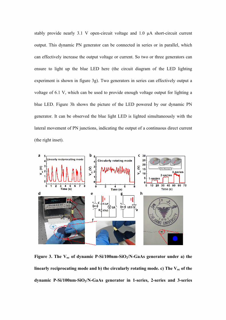
stably provide nearly 3.1 V open-circuit voltage and 1.0 µA short-circuit current
output. This dynamic PN generator can be connected in series or in parallel, which
can effectively increase the output voltage or current. So two or three generators can
ensure to light up the blue LED here (the circuit diagram of the LED lighting
experiment is shown in figure 3g). Two generators in series can effectively output a
voltage of 6.1 V, which can be used to provide enough voltage output for lighting a
blue LED. Figure 3h shows the picture of the LED powered by our dynamic PN
generator. It can be observed the blue light LED is lighted simultaneously with the
lateral movement of PN junctions, indicating the output of a continuous direct current
(the right inset).
Figure 3. The Voc of dynamic P-Si/100nm-SiO2/N-GaAs generator under a) the
linearly reciprocating mode and b) the circularly rotating mode. c) The Voc of the
dynamic P-Si/100nm-SiO2/N-GaAs generator in 1-series, 2-series and 3-series

with a 6N force, a speed of 6 cm/s. Inset: The schematic image of series
connection of the dynamic PN junctions. d) The captured optical picture of the
capacitor charging experiment, which is measured with Keithley 2010 system. e)
The circuit diagram of charging a capacitor C (0.1µF) with the dynamic
P-Si/SiO2/N-GaAs generator. No additional rectification circuit has been used. f)
The partial enlarged image of the dynamic P-Si/SiO2/N-GaAs generator. g) The
circuit diagram of the LED lighting experiment. h) Pictures taken from video to
show the luminance of a LED powered by our dynamic PN generator. Right
inset: The lighting blue LED powered by the dynamic PN junctions.
As the friction strength between P-Si and N-GaAs is high, which may destroy the
surface of the semiconductor, we have used the layered semiconductors such as
MoS221,33.The diffusing electrons and holes in dynamic P-Si/10nm-AlN/MoS2
junction can also be directionally bound back by the built-in electronic field at the
interface, generating the electricity. As shown in the band diagram of dynamic
P-Si/AlN/MoS2 junction (Figure 4a), under the localized built-in electric field from
MoS2 to P-Si substrate, the diffusing electrons will bound back to the MoS2 and
diffusing holes will bound back to the P-type Si, breaking up the equilibrium of
drift-diffusion current and forming electrical output. The rectification characteristic of
the dynamic P-Si/AlN/MoS2 junction from -5V to 5V is also measured. As shown in
Figure 4b, the interfacial PN junction varies when the P-Si/AlN/MoS2 contact is under
the friction process, which helps testifying the theory proposed above. The fluctuation

of the J-V curve of the P-Si/AlN/MoS2 junction under friction condition is caused by
the destruction and re-establishment of the depletion layer in the dynamic PN junction,
which indicates the generation of the voltage output. Normally, the Jsc as high as 112
A/m2 can be achieved, with the work area of 0.05 mm2, which is about three orders of
magnitude higher than the reported triboelectric nanogenerators25-28. To demonstrate
the power output of our generator, the voltage and current output as a function of
electrical load R have been investigated and shown in Figure 4c. An increasing
voltage and decreasing current density can be measured with the increase of load
resistance. Accordingly, the power density output as a function of electrical load R
have also been investigated and shown in Figure 4d. The peak power density about
130 W/m2 can be found around R equals to 360 kΩ, which is close to the internal
resistance of the PN junction. And the energy-conversion efficiency of the moving
Si/MoS2 junction generator can be calculated to be about 27.1% (as shown in the
Supplementary Note 3). As MoS2 is a lubricating material, dynamic P-Si/AlN/MoS2
PN junction generator shows excellent stability. Notably, as shown in the direct and
continuous voltage and current output of the dynamic P-Si/AlN/MoS2 (Figure 4e and
4f), this dynamic P-Si/AlN/MoS2 generator does not show any obvious degradation
after 60 min of running, demonstrating the potential applications of the dynamic PN
generator. The fluctuation of the continuous voltage and current output is caused by
the vibration of the pressure and moving speed.

Figure 4. a) The band diagram and carrier dynamic process of the dynamic
P-Si/AlN/MoS2 generator. b) The J-V curve of the dynamic P-Si/AlN/MoS2
junction with a 6N force. The contact area is 0.05 mm2. c) Voc and Jsc output as a
function of electrical load R. Both the Voc and Jsc are the peak value of voltage
and current output. Insert: equivalent circuit. d) The power density output as a
function of electrical load R. e) The direct and continuous voltage and f) current
output of the dynamic P-Si/AlN/MoS2 generator for 60 min continuously, with an
electrical load R of 680 kΩ.
We have demonstrated a novel direct-current generator based on the dynamic PN
junction, where two semiconductors with different Fermi level slide with each other.
The mechanism is proposed based on the built-in electric field bounding back
diffusing carriers emitted by the destruction and re-establishment of the depletion
layer in dynamic PN junctions, which breaks the equilibrium between the drift current
and diffusion current. The voltage, current and output power of the dynamic PN

generator can be further enhanced through optimizing the PN junction interface and
designing the semiconductor-insulator-semiconductor structure. Notably, the dynamic
PN generators with high voltage of 5.1V and high current density of 112 A/m2 have
been realized based on MoS2/AlN/Si structure. Especially, this dynamic
P-Si/AlN/MoS2 generator does not show obvious degradation after 60 min of running,
demonstrating the unique mechanism and stability of the dynamic PN generator. This
novel dynamic PN generator with sufficient current density has many promising
applications in many fields where the mechanical energy is available.
METHODS
Devices fabrication. Firstly, the double side polished N-type GaAs wafer was
dipping into 10 wt% HCl for 10 min to remove the native oxide layer in the surface
and washed by deionized water. Then Au (100 nm) electrode was fabricated with
magnetron sputtering on one side of GaAs wafer. Similarly, the single side polished
P-type and N-type Si substrate were dipping into 10 wt% HF for 10 min to remove the
native oxide layer in the interface and then washed by deionized water. Ti/Au (20
nm/50 nm) electrode was fabricated with magnetron sputtering on the unpolished side
of Si substrate and MoS2 flake. The N-type GaAs or MoS2 was pressed closely on the
P-type Si substrate by the hand, making sure a solid electrical contact between N-type
GaAs/MoS2 and P-type Si substrate can be achieved. The AlN layer on P-type Si is
fabricated with Physical Vapor Deposition method. And the SiO2 layer on P-type Si is
fabricated with thermal oxidation method in 1100℃.
Physical characterization methods. The microscopic image of the generator was

characterized with ZEISS optical microscopy. The current-voltage (I-V) curve of the
PN junction was measured with Keithley 2400 system. The real-time voltage and
current output were recorded in real time by a Keithley 2010 system, which was
controlled by a LabView-based data acquisition system with a sampling rate of 25 s-1.
The Keithley 6485 picoammeter was also used to verify accuracy of current output,
which was controlled by a LabView-based data acquisition system with a sampling
rate of 100 s-1. The force was measured with the pressure meter.
Data availability
The data that support the findings of this study are available from the corresponding
author upon reasonable request.
References
1. Faraday, M. XVII. On a peculiar class of acoustical figures; and on certain forms assumed by
groups of particles upon vibrating elastic surfaces. Philos. Trans. R. Soc. London 121, 299-‐340
(1831).
2. Van, Atta, L. C., Northrup, D. L., Van, Atta, C. M. & Van, De, Graaff, R. J. The Design,
Operation, and Performance of the Round Hill Electrostatic Generator. Phys. Rev. 49,
761-‐776 (1936).
3. Wang, Z. L. & Song, J. Piezoelectric Nanogenerators Based on Zinc Oxide Nanowire Arrays.
Science 312, 242-‐246 (2006).
4. Fan, F. R., Tian, Z. Q. & Wang, Z. L. Flexible triboelectric generator. Nano Energy 1, 328-‐334
(2012).
5. Zhong, H. et al. Graphene-‐Piezoelectric Material Heterostructure for Harvesting Energy from
Water Flow. Adv. Func. Mater. 27, 1604226 (2017).
6. Park, K. I. et al. Piezoelectric BaTiO3 thin film nanogenerator on plastic substrates. Nano lett.
10, 4939-‐4943 (2010).
7. Wang, Z. L. On Maxwell's displacement current for energy and sensors: the origin of
nanogenerators. Mater. Today 20, 74-‐82 (2017).
8. Li, X. Q. et al. 18.5% efficient graphene/GaAs van der Waals heterostructure solar cell. Nano
Energy 16, 310-‐319 (2015).
9. Green, M. A., Ho-‐Baillie, A. & Snaith, H. J. The emergence of perovskite solar cells. Nat.
Photonics 8, 506 (2014).
10. Zhao, D. et al. Low-‐bandgap mixed tin–lead iodide perovskite absorbers with long carrier

lifetimes for all-‐perovskite tandem solar cells. Nat. Energy 2, 17018 (2017).
11. Henniker, J. Triboelectricity in Polymers. Nature 196, 474 (1962).
12. Peng, J., Kang, S. D. & Snyder, G. J. Optimization principles and the figure of merit for
triboelectric generators. Sci. Adv. 3, 8576 (2017).
13. Baytekin, H. T., Baytekin, B., Hermans, T. M., Kowalczyk. B. & Grzybowski, B. A. Control of
surface charges by radicals as a principle of antistatic polymers protecting electronic circuitry.
Science 341, 1368-‐1371 (2013).
14. Wang, Z. L. Triboelectric nanogenerators as new energy technology for self-‐powered systems
and as active mechanical and chemical sensors. ACS nano 7, 9533-‐9557 (2013).
15. Park, J. Y. & Salmeron, M. Fundamental aspects of energy dissipation in friction. Chem. rev.
114, 677-‐711 (2013).
16. Zhang, Q., Xu, R. & Cai, W. Pumping electrons from chemical potential difference. Nano
Energy 51, 698-‐703 (2018).
17. Schottky, W. The Theory of p-‐n Junctions in Semiconductors and p-‐n Junction Transistors.
Bell Syst. Tech. J. 28, 435-‐489 (1949).
18. Chapin, D. M., Fuller, C. & Pearson, G. A new silicon p‐n junction photocell for converting
solar radiation into electrical power. J. Appl. Phys. 25, 676-‐677 (1954).
19. Sah, C. T., Noyce, R. N. & Shockley, W. Carrier generation and recombination in pn junctions
and pn junction characteristics. P. IRE 45, 1228-‐1243 (1957).
20. Lin, S., Lu, Y., Feng, S., Hao, Z. & Yan, Y. A High Current Density Direct-‐Current Generator
Based on a Moving van der Waals Schottky Diode. Adv. Mater. 0, e1804398 (2018).
21. Liu, J. et al. Direct-‐current triboelectricity generation by a sliding Schottky nanocontact on
MoS2 multilayers. Nat. Nanotechnol. 13, 112-‐116 (2018).
22. Liu, J. et al. Sustained electron tunneling at unbiased metal-‐insulator-‐semiconductor
triboelectric contacts. Nano Energy 48, 320-‐326 (2018).
23. Li, X. et al. Graphene/h-‐BN/GaAs sandwich diode as solar cell and photodetector. Opt.
Express 24, 134-‐145 (2016).
24. Miyazaki, T. & Tezuka, N. Giant magnetic tunneling effect in Fe/Al2O3/Fe junction. J. Magn.
Magn. Mater. 139, L231-‐L234 (1995).
25. Wang, Z. L., Chen, J. & Lin, L. Progress in triboelectric nanogenerators as a new energy
technology and self-‐powered sensors. Energ. Environ. Sci. 8, 2250-‐2282 (2015).
26. Zhu, G. et al. Toward large-‐scale energy harvesting by a nanoparticle-‐enhanced triboelectric
nanogenerator. Nano lett. 13, 847-‐853 (2013).
27. Xu, S. et al. Self-‐powered nanowire devices. Nat. Nanotechnol. 5, 366 (2010).
28. Hu, Y. & Wang, Z. L. Recent progress in piezoelectric nanogenerators as a sustainable power
source in self-‐powered systems and active sensors. Nano Energy 14, 3-‐14 (2015).
29. Chen, X., Xu, S., Yao, N. & Shi, Y. 1.6 V nanogenerator for mechanical energy harvesting using
PZT nanofibers. Nano lett. 10, 2133-‐2137 (2010).
30. Wang, X., Song, J., Liu, J. & Wang, Z. L. Direct-‐Current Nanogenerator Driven by Ultrasonic
Waves. Science 316, 102-‐105 (2007).
31. Yang, R., Qin, Y., Li, C., Zhu, G. & Wang, Z. L. Converting biomechanical energy into electricity
by a muscle-‐movement-‐driven nanogenerator. Nano Lett. 9, 1201-‐1205 (2009).
32. Zhang, Y., Liu, Y. & Wang, Z. L. Fundamental Theory of Piezotronics. Adv. Mater. 23,
3004-‐3013 (2011).

33. Lin, S. et al. Interface designed MoS2/GaAs heterostructure solar cell with sandwich stacked
hexagonal boron nitride. Sci. Rep. 5, 15103 (2015).
Acknowledgements: S. S. Lin thanks the support from the National Natural Science
Foundation of China (No. 51202216, 51502264 and 61774135) and Special
Foundation of Young Professor of Zhejiang University (Grant No. 2013QNA5007).
Author Contributions: S. S. Lin designed the experiments, analyzed the data and
conceived all the works. Y. H. Lu carried out the experiments, discussed the results
and wrote the paper. S. R. Feng, Z. Z. Hao and R. J. Shen discussed the results and
assisted with experiments. All authors contributed to the writing of the paper.
Author Information: Reprints and permission information is available online. The
authors declare no competing financial interest. Readers are welcome to comment on
the online version of the paper.
Supplementary Information is Available in the online website.