Embed Size (px)
Citation preview

Licentiate Thesis
High Performance LNAs and Mixers
for Direct Conversion Receivers in
BiCMOS and CMOS Technologies
By
Tobias Tired
Department of Electrical and Information Technology
Faculty of Engineering, LTH, Lund University
SE-221 00 Lund, Sweden

2
Abstract The trend in cellular chipset design today is to incorporate support for a larger
number of frequency bands for each new chipset generation. If the chipset also
supports receiver diversity two low noise amplifiers (LNAs) are required for each
frequency band. This is however associated with an increase of off-chip
components, i.e. matching components for the LNA inputs, as well as complex
routing of the RF input signals. If balanced LNAs are implemented the routing
complexity is further increased. The first presented work in this thesis is a novel
multiband low noise single ended LNA and mixer architecture. The mixer has a
novel feedback loop suppressing both second order distortion as well as DC-offset.
The performance, verified by Monte Carlo simulations, is sufficient for a
WCDMA application. The second presented work is a single ended multiband
LNA with programmable integrated matching. The LNA is connected to an on-
chip tunable balun generating differential RF signals for a differential mixer. The
combination of the narrow band input matching and narrow band balun of the
presented LNA is beneficial for suppressing third harmonic downconversion of a
WLAN interferer. The single ended architecture has great advantages regarding
PCB routing of the RF input signals but is on the other hand more sensitive to
common mode interferers, e.g. ground, supply and substrate noise. An analysis of
direct conversion receiver requirements is presented together with an overview of
different LNA and mixer architectures in both BiCMOS and CMOS technology.

3
Acknowledgements
I would like to thank my supervisor Pietro Andreani at EIT for first of all
arranging the position as industry PhD student for me. Secondly I am also grateful
for the time he spent reviewing the two papers presented in this Licentiate Thesis.
Furthermore I would also like to thank my assisting supervisor Markus Törmänen
for reviewing the thesis.
I am also extremely grateful to my wife, Maria and my three children Axel, Nils
and Signe for allowing me to spend time writing the two included papers and the
thesis during vacations and evenings.
Tobias Tired
Lund, 2012-02-10

4
Table of Contents
Abstract ................................................................................................................. 2
Acknowledgements ............................................................................................. 3
Table of Contents ................................................................................................ 4
Preface ................................................................................................................... 7
Abbreviations ..................................................................................................... 9
Part I General Introduction ......................................................................... 11
1 Introduction .............................................................................................. 12 1.1 Background ................................................................................................. 12 1.2 Cellular radio systems duplexing architectures ................................. 14 1.3 Silicon process technology choices ......................................................... 15 1.4 Thesis structure ....................................................................................... 16
2 Receiver requirements ........................................................................... 17 2.1 Introduction ................................................................................................ 17 2.2 Sensitivity ..................................................................................................... 17 2.3 Single sideband and double sideband noise figure ............................ 19 2.4 Noise folding ................................................................................................ 19 2.5 Intermodulation ......................................................................................... 20
2.5.1 Introduction........................................................................................................ 20 2.5.2 Second and third order nonlinearities ........................................................ 20 2.5.3 Third order nonlinearities .............................................................................. 21
2.6 Compression................................................................................................ 22 2.7 Desensitization ............................................................................................ 23 2.8 Harmonic mixing ....................................................................................... 24 2.9 Reciprocal mixing ...................................................................................... 24 2.10 Second order distortion in FDD systems .............................................. 25 2.11 Third order distortion in FDD systems ................................................ 26 2.12 Cross modulation in FDD systems ......................................................... 26
2.12.1 Cross modulation from TX-leakage ..................................................... 26 2.12.2 Cross modulation in FDD systems with zero-IF receivers ............ 28
2.13 Linearity requirements in E-GSM/GPRS/EDGE systems............... 29
3 Receiver architectures ............................................................................ 30 3.1 Introduction ................................................................................................ 30 3.2 Image rejection ........................................................................................... 30 3.3 The direct conversion receiver ............................................................... 31

5
3.3.1 Direct conversion receiver architecture .................................................... 31 3.3.2 Direct conversion receiver drawbacks ...................................................... 31
3.4 The low-IF receiver ................................................................................... 33 3.5 Receiver architecture summary ............................................................. 34
4 Process technology and device performance .................................... 35 4.1 Introduction ................................................................................................ 35 4.2 Process technology ..................................................................................... 35 4.3 Package technology ................................................................................... 36 4.4 Substrate coupling ..................................................................................... 37 4.5 Basic equations for the MOS and bipolar transistors ....................... 38
4.5.1 Introduction........................................................................................................ 38 4.5.2 MOS transistor equations .............................................................................. 38 4.5.3 Bipolar transistor equations .......................................................................... 39
5 LNA architectures ................................................................................... 41 5.1 Introduction ................................................................................................ 41 5.2 Single ended versus differential LNA architectures.......................... 42 5.3 LNA architectures in CMOS technology ............................................. 42
5.3.1 Common-source LNA with inductive degeneration ............................. 42 5.3.2 CS-stage LNA with integrated balun ......................................................... 50 5.3.3 The common-gate architecture LNA ......................................................... 51 5.3.4 The resistive feedback CMOS LNA .......................................................... 54
5.4 Noise cancelation ........................................................................................ 55 5.4.1 Introduction........................................................................................................ 55 5.4.2 Noise cancelation with resistive feedback LNA .................................... 56 5.4.1 Noise cancelation with combination of CG- and CS stage ................. 58
6 Mixer architectures ................................................................................ 62 6.1 Introduction ................................................................................................ 62 6.2 Active mixers .............................................................................................. 63
6.2.1 Introduction........................................................................................................ 63 6.2.2 Single-balanced active mixer ....................................................................... 63 6.2.3 Double balanced active mixer ...................................................................... 67
6.3 Passive mixer .............................................................................................. 68 6.3.1 Introduction........................................................................................................ 68 6.3.2 Passive mixer second order distortion ....................................................... 69 6.3.3 Differential passive mixer with four-phase clock .................................. 71 6.3.4 Passive mixer frequency translation .......................................................... 74
7 Future radio architectures .................................................................... 76 7.1 Introduction ................................................................................................ 76 7.2 Duplexer elimination ................................................................................. 76 7.3 E-GSM SAW-filter elimination .............................................................. 77

6
8 Conclusions ............................................................................................... 79
References .......................................................................................................... 80
Part II Included papers ................................................................................. 89
Summary of included papers ........................................................................ 90
Paper I ................................................................................................................ 91
Paper II ............................................................................................................ 120
7
Preface
This licentiate thesis is about some of the work made by me on the topic of linear
LNAs and mixers for direct conversion receivers. The publications have been
made in parallel with my work at the RF technology department at ST-Ericsson.
Having a background in the wireless industry has given me valuable experience
for writing this thesis. To be commercially viable new radio front end architectures
must fulfill hard requirements determined by the 3GPP organization as well as
chip set customers. The front-end requirements are analyzed in the first part of this
work. Several alternative LNA and mixer architectures are also provided. In the
second part, two of my publications regarding linear LNAs and mixers are
included. The first paper describes the design and simulations of a single ended
LNA and single ended mixer implemented in BiCMOS technology. The second
paper regards a low noise single ended multiband amplifier with tunable on-chip
matching implemented in CMOS technology. The performance of the published
architectures are well in-line with the front-end requirements that are discussed in
the first part of the thesis.
Included publications
I. T. Tired, “A BiCMOS single ended multiband RF-amplifier
and mixer with DC-offset and second order distortion
suppression”, Springer Analog integrated circuits and
signal processing, vol. 68, no. 3, pp. 269-283, 2011.
II. T. Tired, “Single Ended Low Noise Multiband LNA with
programmable integrated matching and high isolation
switches”, in the proceedings of NORCHIP 2011, ISBN
978-1-4577-0514-4, pp 1-4, Nov. 2011
Other publications
I. Y. Le Guillou, O. Gaborieau, P. Gamand,, M. Isberg,, P.
Jakobsson, L. Jonsson, D. Le Deaut, H. Marie, S.
Mattisson, S, L. Monge, T. Olsson, S. Prouet, T. Tired,
Philips Semiconductors., Caen, France, “Highly integrated
direct conversion receiver for GSM/GPRS/EDGE with on-
chip 84-dB dynamic range continuous-time ΣΔ ADC”,
8
IEEE Journal of Solid State Circuits, vol. 40, no. 2, pp.
403-411, Feb. 2005
II. Luca Vandi, Pietro Andreani, Tobias Tired, Sven
Mattisson, “A novel approach to negative feedback in RX
front-ends”, in the proceedings of NORCHIP 2006, ISBN
1-4244-0772-9, pp. 231-234, Nov. 2006
III. M. Nilsson, S. Mattisson, N. Klemmer, P. Andreani, T.
Tired et al, ”A 9 band WCDMA/EDGE transceiver
supporting HSPA evolution”, in the proceedings of 2011
International Solid State Circuits Conference (ISSCC),
ISBN 978-1-61284-303-2, pp. 366-368, Feb, 2011

9
Abbreviations
LNA Low Noise Amplifier
E-GSM Extended Global System for Mobile communication
LTE FDD Long Term Evolution Frequency Domain Duplex
LTE TDD Long Term Evolution Time Domain Duplex
WCDMA Wideband Code-Division Multiple Access
PCB Printed Circuit Board
SAW Surface Acoustic Wave
RFIC Radio Frequency Integrated Circuit
WLAN Wireless Local Area Network
GPS Global Positioning System
WiMAX Worldwide Interoperability for Microwave Access
TD-SCDMA Time Division Synchronous Code Division Multiple Access
TD-CDMA Time Division Code-Division Multiple Access
CMOS Complementary Metal Oxide Silicon
BiCMOS Bipolar Complementary Metal Oxide Semiconductor
SNR Signal-to-noise ratio
BER Bit-error-rate
QAM Quadrature Amplitude Modulation
GPRS General Packet Radio Service
EDGE Enhanced Data Rates for GSM Evolution

10
LO Local Oscillator
CW Continuous Wave
AM Amplitude modulation
VCO Voltage Controlled Oscillator
PCB Printed Circuit Board
Wi-Fi Wireless Fidelity

11
Part I
General Introduction

12
CHAPTER 1
1 Introduction
1.1 Background
The first chipsets targeted for E-GSM [1] in the 1990s only supported one single
frequency band. Since then there has been a tremendous growth in the number of
subscribers of different cellular radio systems. This development has also resulted
in an increase in the number of frequency bands a cell phone must support since
different operators over the word have licenses for different parts of the frequency
spectrum. For LTE FDD [2], [3] receive frequency bands between 700MHz and
2700MHz are defined while LTE TDD [2], [3] operates in bands between
1800MHz and 3800MHz. For the cell phone user multiband operation offers great
advantages while moving across operator regions but for the chipset manufacturer
multiband support also results in increased complexity of the RF front end, both
on-chip and on the PCB. The increased complexity also increases the importance
of designing new front end solutions to keep the cost low for the complete radio
transceiver. However, new innovative solutions are always benchmarked against
old architectures in terms of current consumption, performance and die area
thereby making the implementation of new ideas a very challenging task. Both
paper I and II in this thesis concerns single ended LNA and mixer architectures.
The single ended topology is used to reduce the complexity of the multiband front
end.
The illustration of the multiband direct conversion receiver [4], [5] in Fig.1 is
simplified and only shows two LNAs in the primary and diversity receiver chains.
In reality an implementation that covers the majority of the WCDMA or LTE
frequency bands plus the E-GSM bands contains a larger number of LNAs. The
mixer is however as illustrated shared between the LNAs. The received RF signal
is downconverted in the mixer and low-pass filtered in the baseband filter. An
analog to digital converter, ADC, converts the analog signal into a bit stream for
subsequent processing. The introduction of antenna diversity [6] doubled the
number of required LNAs. When support for antenna diversity is implemented the
receiver contains two independent receiver chains connected to separate antennas
as depicted in Fig.1. In e.g. urban environments the radio signal is reflected against
buildings and destructive interference can occur due to multipath propagation.
Having two receivers connected to different antennas separated by a small distance
reduces the impact of deep fading dips significantly.

13
Fig.1. Multiband direct conversion receiver with primary and diversity receiver chains
Each RF input, except the diversity inputs, needs a dedicated duplexer for the
supported frequency band if the radio system is operating in full duplex e.g.
WCDMA [3] and LTE [3]. The purpose of the duplexer is to attenuate the
transmitted signal from the power amplifier, denoted PA in Fig. 1, in order for this
signal not to compress the receiver. If the RF input is used for a TDD [3] system
like E-GSM a SAW filter is required in order to attenuate the out of band
interferers [7]. Typically the duplexer or SAW-filter is required to be matched to
50 Ω impedance in a single ended architecture. If a differential LNA is used the
RX impedance is higher, e.g. 100 Ω or 200 Ω. Each LNA normally needs off-chip
matching components to fulfill the matching requirement. This adds both cost and
PCB area. A solution with programmable on-chip matching is presented in paper
II. The PCB routing of the RF input signals from the antenna switch, through the
duplexers, to the RFIC becomes increasingly more complex as more frequency
bands are added.
The direct conversion receiver radio architecture has been the dominating
architecture in cellular RF chipsets for more than 10 years. It has a lot of
advantages but also some drawbacks, especially in a FDD radio system. The main
advantage is that the IF-filter present in the superheterodyne receiver [4] is

14
eliminated. The drawback is the receiver sensitivity to second order distortion. In
radio systems like WCDMA and LTE the transmitter and receiver are on
simultaneously. The transmit signal is a digitally modulated signal that contains
both amplitude and phase modulation. A small part of the transmit signal leaks
into the receiver where the amplitude part of the modulation together with second
order distortion in the LNA and mixer will cause an in-band interferer that cannot
be removed and therefore causes the bit-error-rate (BER) of the receiver to
increase for high transmit powers. This is troublesome since the typical scenario
when transmitting with full power coincides with the fact that high sensitivity is
also required, i.e. the terminal is very far from the base station. In Paper II a single
ended mixer is presented with a feedback loop that suppresses second order
distortion. A second drawback associated with the direct conversion receiver is
that this architecture is sensitive to low frequency flicker noise. A third drawback
of this architecture is the impact of DC-offsets in the receiver chain on the receiver
performance [5].
The low noise amplifier (LNA) and mixer are the key building blocks when
designing a receiver. By designing these two blocks with high performance
regarding e.g. noise figure, gain and linearity, the specifications of the succeeding
blocks, i.e. baseband filter and the analog to digital converter (ADC), can be
relaxed. Designing high performance LNA and mixers are therefore of highest
importance since these building blocks determine many of the overall system
parameters of the radio receiver, e.g. sensitivity and blocking.
Lately coexistence issues [8] between cellular systems and other radio
technologies like WLAN [8], Bluetooth [1] and Global Positioning System (GPS)
have been getting higher attention since support for these radio standards are now
more frequently integrated in the cell phone. In a handheld device there are
typically one antenna for the cellular transceiver and another antenna for e.g.
WLAN in close proximity. The isolation between these antennas is rather low, in
the range of 10-15dB, resulting in that a large interferer will leak into the cellular
receiver. This can result in receiver performance degradation, especially if a
broadband LNA without selectivity is used. There are however several ways to
reduce this interferer by novel LNA and mixer design.
1.2 Cellular radio systems duplexing architectures
All standards for cellular communications systems specify a way to send and
receive data simultaneously. This is denoted as duplexing. There are two basic
concepts to achieve this, FDD, frequency division duplex and TDD, time division
duplex. In TDD systems the same frequency is used both to receive and transmit
but transmission and reception occurs at different time slots. In FDD systems the
receiver and transmitter are using different frequencies separated by the duplex
distance. Some cellular standards have both a TDD and a FDD mode, i.e. WiMAX

15
[10] and LTE [3]. Typical TDD systems are E-GSM [1], Time Division Code-
Division Multiple Access (TD-CDMA) [2], Time Division Synchronous Code
Division Multiple Access (TD-SCDMA) [2], and LTE TDD [3]. WCDMA [3] and
LTE FDD [3] are well known FDD systems.
There are advantages and drawbacks related to both TDD and FDD systems. The
fact that the transmitter and receiver are simultaneously turned on in a FDD
system increases the requirements on the receiver since it must be designed in such
a way that it can withstand any performance degradation caused by transmit
signal. In order to relax the requirements on the receiver a duplexer is connected
after the antenna to separate the transmit and receive frequencies. FDD systems
must have a frequency distance between the transmit and receive frequencies that
is large enough to achieve enough filtering in the duplexer. On the other hand a
TDD system needs a distance in time to separate the transmit and receive signal
[11]. One drawback associated with TDD systems is that the time distance must
increase if the distance between the base station and the mobile is large, i.e. in
large cells [12]. This thesis only considers radio architecture issues related to FDD
systems.
1.3 Silicon process technology choices
Today the RF CMOS technology is the dominating process choice for the wireless
industry. For ASICs that are to be implemented in high volume consumer products
cost is the main driver for choosing process technology. Some years ago when RF
CMOS devices were not performing as well as their bipolar counterparts the
BiCMOS technology was the technology of choice offering both high performance
devices for RF design as well as CMOS devices for the digital part. Advances in
RF CMOS process technology has resulted in devices with a transit frequency (fT)
exceeding 300GHz in the 28nm process node [13]. Devices with low Fmin are
available that enables the design of low noise amplifiers. The main difference
compared to digital CMOS is that the RF CMOS process has a process option with
low resistance metal layers in order to implement on chip inductors with high Q-
values. RFICs developed today include an increasingly large digital part for each
generation making future process scaling important for cost effectiveness. The
BiCMOS technology has evolved into the silicon germanium (SiGe) BiCMOS
process [14]. With this technology high performance heterojunction [14] devices
are available with high fT. SiGe BiCMOS is popular for designing e.g. power
amplifiers due to its higher breakdown voltages compared to RF CMOS as well as
lower power consumption [14]. The LNA and mixer described in Paper I of this
thesis is implemented in BiCMOS technology while the LNA presented in paper II
is designed in a 90nm CMOS process.

16
1.4 Thesis structure
The first part of the thesis provides the theoretical background that constitutes the
base for the two included publications. The radio requirements, e.g. sensitivity,
intermodulation and compression are described in chapter 2. An overview of
receiver architectures besides the direct conversion receiver is provided in chapter
3. In chapter 4 key device parameters are compared for bipolar and CMOS
technology. In chapter 5 the package technology evolution from wire-bonded to
wafer-level packaging is described. Different LNA architectures, i.e. single-ended,
balanced, narrow-band, broadband architectures, are described in chapter 5
together with the key LNA performance parameters. In chapter 6 the mixer non-
idealities are described together with a comparison between different mixer
architectures, i.e. active mixers and passive mixers in their single ended and
double balanced versions. Future radio architectures targeted towards SAW-less
E-GSM receivers and FDD systems without duplexers are described in chapter 7.
The conclusions are given in chapter 8.
In the second part the two included publications are discussed. Paper I describes
the design and simulation of a novel single ended LNA and mixer designed in
BiCMOS targeted for direct conversion architectures. The single ended mixer has
a feedback loop around the mixer switching core to reduce the second order
distortion. The third order distortion is minimized through a feedback loop in the
mixer transconductance stage. Paper II is a conference paper that describes the
design of a single ended multiband CMOS LNA with integrated matching
inductor. The matching can be programmed for different frequency bands using
switched capacitors. The different band inputs are connected to the multiband
LNA through programmable switches that provide both high isolation and low on-
resistance depending on which mode they are in.

17
CHAPTER 2
2 Receiver requirements
2.1 Introduction
Radio communication standards, such as GSM/EDGE [15], WCDMA, LTE and
WiMAX use a variety of modulation schemes for transmitting and receiving data.
The requirements on the signal-to-noise ratio, SNR, at the detector to achieve a
certain bit-error-rate (BER) [16] are therefore different. High data rates in the
downlink using modulation schemes as e.g. 64-QAM [16] are actually only
possible to achieve when the signal strength is high. The receiver requirements on
the individual blocks will also depend on which architecture is used. The zero-IF
architecture is the most commonly used but the linearity requirements on the LNA
and mixer are harder compared to a super heterodyne topology. In this chapter a
zero-IF architecture is assumed when the requirements are analyzed.
2.2 Sensitivity
One of the most important metrics of the receiver is its sensitivity [17]. The
receiver sensitivity if defined as the minimum input radio signal that results in a
certain bit-error-rate. Typically a receiver of today has a sensitivity that is better
than -110dBm. Even though such high sensitivity is not required by
standardization organs, e.g. 3GPP [3], the metric is used to compare radio
architectures between competitors. A high sensitivity is beneficial when designing
a cellular radio network since high sensitivity means that the radio base stations do
not have to be that densely located that would have been the situation if the
terminals within the network would have had lower sensitivity.
The sensitivity of the receiver is affected by several parameters:
- the noise figure, NF, of the integrated receiver
- the insertion loss in the antenna switch receive path
- the insertion loss in the external filters, i.e. the E-GSM SAW filters and
the duplexers for FDD systems

18
- the required minimum carrier to noise and interference ratio, C/(N+I) for
the detector
The stringent requirements on sensitivity strongly limit the radio architectures that
are possible to implement in order to achieve a sensitivity that is as high as
-110dBm. Regarding e.g. LNA architectures, topologies that have advantages such
as broadband input matching and high linearity as the common-gate architecture
are not often implemented in a cellular terminal. This is due to that the noise figure
of the common-source LNA is slightly lower than for a common-gate LNA under
certain bias conditions and operating frequencies [18]. In the link budget the
receiver noise figure is balanced against the requirements for linearity. Too high
gain in the first stages of the receiver, i.e. the LNA and mixer is advantageous for
the total noise figure but the linearity is usually compromised resulting in an
overall reduction of the carrier to noise and interference ratio. Typically the
integrated receivers of today have a noise figure of 2.5-3dB including the noise
from the external matching components for the LNA.
Thermal noise in the resistance of the signal source puts a fundamental limit on the
minimum input signal that can be detected by the receiver [17]. When the power
of the signal is reduced below the noise level of the source resistance the signal
can no longer be distinguished from the noise. The available noise power PNA [17]
is defined by (1) where k equals Boltzmann’s constant (1.38e-23J/K), T is the
absolute temperature in Kelvin and f equals the noise bandwidth in Hz.
fkTPNA (1)
At T=T0=290K the available noise power PNA with f = 1Hz equals 4.00e-21W or
-174dBm. The noise figure (2) of the receiver is defined by the SNR at the
receiver input and output [4].
outsourceRsigoutin SNRPPSNRSNRNF /// _ (2)
Psig is defined as the power of received signal per unit bandwidth and PR_source is
the noise power of the source resistance per unit bandwidth. Solving for Psig and
integrating over a certain bandwidth f=B gives the signal power Psig_BW.
BSNRNFPP outsourceRBWsig __ (3)
The receiver sensitivity can be calculated using equation (3) and the minimum
required SNR value for the detector [4]. The noise power of the source resistance
PR_source is then equal to -174dBm/Hz.
BSNRNFPP dBdBHzdBmsourceRysensitivit log10min_/__ (4)
Inserting typical values for E-GSM, i.e. NF=3.5dB including SAW filter and
antenna switch, SNRmin_dB =10dB and B=135 kHz then gives a sensitivity of
-109dBm which is approximately the performance of a receiver today.

19
2.3 Single sideband and double sideband noise figure
The measured noise figure of the direct conversion receiver is given by the double
sideband noise figure, NFDSB. With this definition of noise figure the image and
the wanted RF signal are down converted to the same baseband frequency. With
the single sideband noise figure definition, NFSSB, noise at the image frequency is
downconverted to the same baseband frequency as the wanted signal. However,
since there is no signal at the image frequency for the single sideband noise figure
definition, the SNR of the baseband signal decreases. The noise figure definitions
[4] are outlined in Fig. 2. Compared to the single sideband noise figure, NFSSB,
NFDSB is 3dB less than NFDSB if the noise level at the wanted and image frequency
are the same.
Fig. 2. Single and double sideband noise figure definitions
2.4 Noise folding
The mixer LO signal is a square wave, i.e. ideally its Fourier transform only
contains odd harmonics of fLO. In a mixer noise at odd harmonics of fLO is down
converted to baseband frequencies as well [17]. The degradation of the noise
figure due to noise folding can be significant, especially if a broadband LNA is
used. The programmable active mixer in paper I uses a tunable low-pass filter in
the transconductance amplifier to attenuate the noise at 3fLO.

20
2.5 Intermodulation
2.5.1 Introduction
Intermodulation is a key parameter when defining the receiver requirements. The
nonlinearities of the receiver can generate in-band intermodulation distortion from
two interfering signals that are located outside the channel bandwidth. The
interfering signals can originate from the transmitted signals from the base station
to neighboring cellular terminals, from the transmitter of the own terminal or from
the transmitter of other terminals. Different radio communications systems
deployed in the same area might cause undesired interaction.
2.5.2 Second and third order nonlinearities
2.5.2.1 Second order nonlinearities
The interferer is in certain cases a modulated signal that contains both AM and FM
modulation. The AM modulation of the signal can be represented by a two-tone
interferer with two close frequencies, fTX1 and fTX2, separated by the modulation
frequency. For WCDMA or LTE the largest modulated signal is the TX leakage
signal into the LNA through the finite isolation of the duplexer. The maximum
receiver IM2 level due to TX-leakage is specified in a 3GPP test case defining the
minimum receiver sensitivity while transmitting at full power, i.e. 24dBm. This is
depicted in Fig. 3 with second order distortion generated at the interferer
difference frequency 212 TXTXIM fff [19].
Fig. 3. Second order distortion with AM modulated TX-leakage
The nonlinear system consisting of the LNA and mixer can be represented with a
mixer output signal )(ty and an input signal )(tx . If only second and third order
nonlinearities are accounted for the output signal is given by (5).
)()()()( 3
3
2
21 txatxatxaty (5)
21
If the input signal is the two-tone interferer at 1 and 2, )(tx is given by (6)
where A is the signal amplitude of the interferers.]
)cos()cos()( 21 tAtAtx (6)
The second order nonlinearity will create second order distortion products, )(2 ty
defined by (7) [20]
)))cos(())cos(()2cos(2
1)2cos(
2
11()( 212121
2
22 ttttAaty (7)
The second order intermodulation products are created at frequencies 1 +2,
1 -2 and DC [19], [20]. The power of the intermodulation products is calculated
by squaring and integrating the contributions in (7). In power the IM2 products are
then distributed as 50% (-3dB) at DC, 25% (-6dB) at 1 +2 and 25% (-6dB) at
1 -2. With the second order intercept point referred to the input denoted as IIP2
and if each of the two input tones has the power P, the following applies in log-
scale for the second order intermodulation product )_(2_ 21 ffIMiP calculated back to
the LNA input [19]
2)_(2_ 221
IIPPP ffIMi (8)
2.5.3 Third order nonlinearities
If the two-tone input signal is given by (9) with different amplitudes A1 and A2 the
third order nonlinearity of (5) will create low frequency third order
intermodulation products given by (10) [20]. The interferer scenario is depicted in
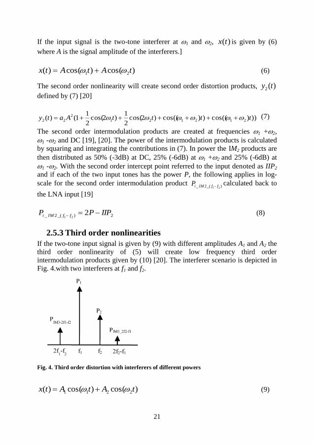
Fig. 4.with two interferers at f1 and f2.
Fig. 4. Third order distortion with interferers of different powers
)cos()cos()( 2211 tAtAtx (9)
22
Third order intermodulation products will be generated at 2f1-f2, 2f2-f1, 2f1+f2 and
2f2+f1. Only the two first products as defined by (10) are of interest in a receiver.
...))2cos(4
3))2cos((
4
3)( 121
2
23212
2
133 tAAatAAaty (10)
With the input third order intercept point defined as IIP3, the IM3-product at
22-1 in log-scale is given by (11) [20].
3122_ 22123
IIPPPPIM (11)
For the IM3-product at 21-2 (12) applies [20].
3212_ 22213
IIPPPPIM (12)
Setting P1 = P2 = P gives the intermodulation product defined by (13).
3233
IIPPPIM (13)
2.6 Compression
Compression of a receiver occurs when the input signal level is high enough that
the receiver is close to clipping. The nonlinearities of the receiver are then
increasing rapidly with input power and the gain is reduced. The compression
point, CP1dB, is defined as the input power where the gain has dropped by 1dB.
Typically there are requirements on two different compression cases. In the first
case the wanted signal is compressing the receiver. This can occur if the cellular
terminal is close to the base station. The maximum power of the WCDMA wanted
signal is -25dBm [3] With a strong wanted signal the gain of the receiver chain can
be reduced while still maintaining a SNR that is high enough that the bit-error rate,
BER, is not affected. Typically the gain in both the LNA and the baseband filter is
programmable. In paper I the gain switch is implemented in the transconductance
amplifier. In paper II the gain of the LNA is altered by reducing the bias current of
the LNA. The 50 Ω input matching is maintained by tuning the on-chip matching.
In the second case an out of band signal or a signal close to the received channel is
the interferer that compresses the receiver. The receiver must be able to handle this
signal level otherwise desensitization [4] will occur. For interferers that are outside
the channel bandwidth compression typically occurs before the low pass baseband
filter, i.e.in the LNA and mixer. To avoid cross compression of the small wanted
signal by the interferer the biasing current must be increased.
The external filters preceding the LNA, i.e. the SAW filter in GSM and the
duplexer in WCDMA and LTE FDD attenuate out of band interferers. In GSM the
largest interferer is at 0dBm [3]. In WCDMA and LTE it is reduced to -15dBm
[3], [20]. Without the GSM SAW filter the current consumption of the LNA would
become unreasonably high. The requirement that is defining the GSM cross
compression point is instead the blocking signal at f=3MHz from the carrier. For

23
this interferer CP1dB should be at least -23dBm [3]. For FDD systems, e.g.
WCDMA and LTE FDD the required compression point is defined by the
transmitter signal that leaks through the duplexer. A duplexer typically has a TX to
RX attenuation of 50-55dB. The maximum output power at the antenna is
+24dBm [3]. If the combined insertion loss in the TX path of the duplexer plus the
antenna switch is 2dB the required output power from the power amplifier is
+26dBm. If a duplexer isolation of 52dB is assumed the TX power is -26dBm in
RX. This is the largest interferer that the WCMDA/LTE receiver must handle. The
-15dBm out-of-band interferer is attenuated by the duplexer to –around 45dBm
[20] The instantaneous power is higher though due to that certain modulation
schemes, have a crest factor [21] that increases the peak power.
Recently there have been a lot of research activities in receiver architectures that
can handle large interferers without depending on external SAW filters in
GSM/GPRS/EDGE [22], [23], [24] or duplexers in WCDMA/LTE [25], [26]. As
the cellular terminal supports an increasing number of frequency bands, the cost of
the external filters is in the same range as the RF ASIC itself.
2.7 Desensitization
Receiver desensitization [4] is a reduction of the receiver sensitivity when a large
interferer is present simultaneously as the desired signal. The desensitization is a
combination of several effects. When the amplitude of the interferer is increased
above a certain level the gain of the wanted signal starts to decrease. This is
denoted as cross compression of the receiver. If the gain of the LNA and mixer is
reduced the noise of the baseband filter and ADC will be more visible, i.e. the
receiver noise figure is increased. In a FDD system like WCDMA or LTE FDD
the worst interferer is the own modulated transmitter signal. Second order
nonlinearities in the receiver will generate an in-band interferer that will cause
desensitization. The active mixer presented in paper I is programmable in two
modes depending on the TX power. For low TX power the transconductance stage
is DC coupled to the mixer switching core. For high TX power the low frequency
IM2 products are heavily attenuated using AC coupling. The current consumption
of the mixer is significantly reduced in the DC coupled mode. Another effect
causing receiver desensitization is the down conversion of the TX phase noise at
the receiver LO frequency. The TX noise leaks into the receiver through the finite
isolation of the duplexer. This puts requirements on the VCO, the LO path and the
IQ modulator [25]. At present a typical receiver has an overall noise figure of 2.5-
3dB and is specified with 0.5-1dB noise figure degradation due to the TX-leakage
at full output power. [25]. The duplexer with its high TX to RX isolation reduces
the desensitization but also adds insertion loss [26].

24
2.8 Harmonic mixing
The mixer LO signal is a square wave, i.e. ideally its Fourier transform only
contains odd harmonics of fLO. The wanted RF signal is down converted with the
fundamental tone of the LO signal to a baseband signal. However, the harmonics
down convert RF signals to exactly the same baseband signal. This will deteriorate
the receiver performance especially when large interferers are present at n*fLO. The
square wave shape of the LO signal is necessary in order to achieve a low noise
figure and high linearity of the mixer [4]. The interferer that is down converted by
harmonic mixing could be generated within the cellular terminal itself. Radio
communication systems like e.g. WLAN [27] will in the nearby future more often
be integrated in the terminal together with the cellular radio. These coexistence
issues [28] become increasingly complex as the cellular terminal supports more
communication standards. At present a lot of research is being done on SAW-less
receivers [22], [23], [24] with no filtering before the LNA. In these novel
architectures harmonic mixing is one of the main obstacles. There are several ways
to address the issue with harmonic down conversion. One way is not to use
broadband LNAs without selectivity. The LNA in paper II uses programmable
narrow band matching in combination with a tunable narrow band balun to reduce
the harmonic mixing at 3fLO. Another way is to use an eight phase mixer [29] that
mimics the sinusoidal LO signal using a sequence of eight square-wave shaped LO
signals. With this solution the noise figure and linearity is not compromised.
2.9 Reciprocal mixing
Reciprocal mixing [4] is an undesired effect that result in downconversion of an
interferer by the phase noise of the LO signal. This is depicted in Fig. 8 outlining
the interferer scenario with a small wanted signal and a large interferer.
Fig. 5. Reciprocal mixing
The interferer will be downconverted to DC by the phase noise. With a high power
interferer the noise in the downconverted desired channel will be significant. The
reciprocal mixing effect sets a limit on the maximum phase noise at the interferer
frequency.

25
2.10 Second order distortion in FDD systems
For WCDMA there are both in-band and out-of-band requirements that are defined
by the receiver second order linearity. The in-band requirements are defined by the
in-band blocking test with a modulated blocking signal at either 10MHz or 15MHz
offset from the wanted signal. Second order distortion generates intermodulation
products inside the bandwidth of the wanted signal. It is however not the in-band
requirement that defines the minimum IIP2 of receiver, this is determined by the
out-of-band requirement, i.e. the own TX-leakage. The receiver IM2 level due to
TX-leakage is tested in a 3GPP standard test case [3] that specifies the minimum
required sensitivity while the TX signal is at maximum power level, i.e.+24dBm,
at the antenna. Sensitivity to second order distortion is one of the most important
drawbacks with the zero-IF receiver [5]. As depicted in Fig. 3 second order
intermodulation products are created by the AM-modulated TX-leakage. There are
four mechanisms that generate second order distortion from AM-modulated TX-
leakage in a zero-IF receiver [5], [20], [32]-[37].
1. RF self-mixing
The RF signal can leak to the LO signal in the mixer through parasitic coupling in
the mixer switching core devices [5]. If the LO-amplitude is not high enough the
mixer behaves like a linear multiplier [30] and the mixer output will contain a
signal that is proportional to the square of the input signal i.e. an IM2 product.
2. Second order nonlinearity in the mixer transconductance stage
The transconductance transistors in the active mixer have a second order
nonlinearity generating a low frequency IM2 product that leaks to the mixer output.
If the mixer switching core, LO driver and mixer load is perfectly balanced, i.e.
without mismatch the second order intermodulation will cancel at the differential
mixer output [31]. Mismatch is however always present resulting in second order
distortion at the mixer output.
3. Second order nonlinearity of the switching mixer core devices
The switching mixer core devices have a second order nonlinearity. The IM2
product generated from the core devices is common-mode, i.e. without
simultaneous mismatch in the switching core devices, the LO driver or the mixer
load, the second order intermodulation will cancel at the differential mixer output.
4. Cross modulation of the LO-leakage
The AM-modulation of the TX-leakage at the mixer core RF input will transfer to
the LO-leakage at the mixer RF input through the cross modulation mechanism
[20], [32]-[37]. Downconversion of the AM-modulated LO-leakage with the LO-
signal itself will generate a differential mixer output signal at the IM2-frequency.

26
2.11 Third order distortion in FDD systems
The worst third order intermodulation case is when an interferer is present at half
the duplex distance between the RX and TX frequency [20] as depicted in Fig. 6.
The third order nonlinearity of the LNA and mixer will then create an
intermodulation product at the RX frequency.
Fig. 6. Third order intermodulation from TX-leakage and half duplex interferer
With a TX-leakage into the LNA of power P1, a half duplex interferer of power P2
and a third order input intercept point IIP3, the third order intermodulation product
at the LNA input, 3_ IMiP , is given by (20)
)(2)()(2)( 3123_ dBmIIPdBmPdBmPdBmP IMi (14)
The in-band IIP3 requirement is determined by the adjacent channel selectivity
(ACS) test case [3] with two blocking signal signals at 3.5 MHz and 5.9 MHz
from fLO. The out-of band IIP3 requirement depicted in Fig. 8 however still
determines the linearity.
2.12 Cross modulation in FDD systems
2.12.1 Cross modulation from TX-leakage
Cross modulation [20], [30]-[35] is defined as the transfer of the AM-modulation
of an interferer on to a simultaneously present not modulated signal. The
modulation transfer is governed by the third order nonlinearity of the system.
However, in relation to the power of the modulated interferer the cross modulation
power is seen as a second order effect. If the input signal to the receiver, )(tx , is
the sum of an un-modulated interferer, )(1 tx , and the AM-modulated TX-leakage,
)(2 tx , the summed input signal leakage, )(tx , is given by (14).
)cos()(1)cos()( 211 ttmAtAtx TX (15)

27
In (14) )(tm is the amplitude modulation of the TX-leakage. Inserting (15) into (5)
and expanding the third order nonlinearity will give an output intermodulation
product [20] defined by (16).
)cos())(1(2
3)( 1
22
213mod ttmAAatycross (16)
The interferer at frequency 1 is now amplitude modulated by the square of the
amplitude of the TX-leakage as depicted in Fig. 7.
Fig. 7. Cross modulation of a CW interferer by AM-modulated TX leakage
As depicted in Fig. 6 each sideband of the cross modulated signal is at a distance
from the carrier equal to the bandwidth of the AM modulated interferer [31], [35].
If a continuous wave (CW) blocker is close to the desired channel cross
modulation from an AM-modulated interferer will create interference inside the
bandwidth of the desired channel. In FDD systems, e.g. WCDMA and LTE FDD
the strongest AM-modulated interferer is the own TX-signal.
The output cross modulation product (15) is referred to the input by dividing with
the gain a1 of (1). Given the gain a1 and the third order nonlinearity coefficient a3,
the third order intercept point, IP3, is defined as (17).
3
13
3
4
a
aIP (17)
The input cross modulation product, )(mod txcross , is defined in (18).
)cos())(1((2)(
)( 12
3
22
21
1
modmod t
IP
tmAA
a
tytx cross
cross
(18)

28
Converting (17) to log-scale defines mod_ crossiP in power units at the input [31] in
(19). The cross modulation product is linear proportional to the interferer power
and to the square of the TX-leakage.
))()((2)(6 321mod_ dBmIPdBmPdBmPP crossi (19)
Cross modulation is a second order effect that is inversely proportional to the
square of the third order intercept point. As depicted in Fig. 6 the amount of
interference that overlaps the desired channel will depend upon the distance
between the non-modulated interferer as well of the modulation bandwidth of the
TX-signal. The interferer power that overlaps the desired channel will be
downconverted together with the desired channel. As with second order distortion
the cross modulation is proportional to the square of the interferer power. There is
however an important difference. Distortion generated by second order
nonlinearities is common-mode, i.e. device mismatch is required to generate a
differential intermodulation product. Distortion created by cross modulation is
added to the desired RF channel before down conversion. It will therefore appear
as a differential signal at the mixer output, in the same way as the desired channel.
With digital modulation of the TX signal the expression (18) is modified to
include a correction factor [20], [35]. The expression is therefore re-written as
(120) with a correction factor including the 6dB in (19).
))()((2)( 321mod_ dBmIPdBmPdBmPCP factorcrossi (20)
The correction factor depends on the distance between the cross modulated
interferer and the desired channel as well as the modulation of the TX-signal.
2.12.2 Cross modulation in FDD systems with zero-IF receivers
In a zero-IF receiver the local oscillator is set to the same frequency as the centre
of the received RF channel. There is always a certain level of LO-leakage present
at the LNA input acting as an interferer. The cross modulation effect will transfer
the AM-modulation of the TX-leakage to the LO-leakage. The interferer scenario
is now different compared the case with the external CW interferer depicted in
Fig. 7 since a larger fraction of the cross modulation power will coincide with the
desired RF channel. The cross modulation effect with the LO-leakage as the
interferer is depicted in Fig. 8. Given that the bandwidths of the TX and RX signal
are equal, a part of the cross modulated LO-leakage will be outside the RX
channel since the bandwidth of the cross modulated signal is two times the TX
signal. Second order distortion is created by the down conversion of the AM-
modulated LO-leakage. In paper II a feedback loop around the mixer is described

29
Fig. 8. Cross modulation of the LO leakage in a zero-IF receiver by AM-modulated TX-leakage
The mixer is driven by a square wave signal, i.e. the LO signal as well as the
leakage at the LNA input contains odd harmonics of fLO. The LO leakage at the
harmonics of fLO will also be cross modulated. In the mixer the cross modulated
harmonics will be down converted to baseband by the harmonics of the mixer
clock. This effect increases the distortion generated by cross modulation. To
reduce cross modulation either the duplexer isolation should be increased or the
LO leakage should be decreased. Alternatively the IP3 of the system should be
increased.
2.13 Linearity requirements in E-GSM/GPRS/EDGE
systems In the GSM system the IIP2 requirement is defined by an AM-modulated interferer
6MHz from the wanted carrier with a power of -31dBm [3]. The power of the
wanted signal equals -99dBm in this test. The test sets a limit on the BER
degradation with the interferer present. In a multimode receiver supporting both
GSM and WCDMA this is however not the requirement that defines the minimum
required IIP2. This is instead defined by the second order distortion from the TX-
leakage. The IIP3 requirement is defined in a test case with one CW interferer at
800 kHz offset from the wanted signal together with a modulated interferer at
1600 kHz from the wanted signal [3]. In a multimode terminal for both GSM and
WCDMA the hardest requirement defining for third order linearity is defined by
the half duplex interferer [20] in WCDMA.

30
CHAPTER 3
3 Receiver architectures
3.1 Introduction
In the early days of cellular radio communication the super heterodyne receiver [4]
was the dominating receiver architectures. Once the cellular terminal started to
become a high volume product a lot of research efforts both in academia as well as
in the telecommunications industry were targeted towards investigating other
architectures that could have equal performance but with a lower current
consumption and lower cost. As the size of terminals decreased the PCB area
occupied by the radio also became an important parameter. The super heterodyne
architecture requires an external image reject filter [4] plus a second down
conversion mixer and is therefore not a cost effective solution. Nowadays the zero-
IF receiver architecture [5] is found in almost every cellular terminal. Receiver
architectures are typically compared with parameters as current consumption,
sensitivity, image rejection [4], blocker tolerance [3] and the required number of
external components.
3.2 Image rejection
Image rejection [4] is a key parameter when evaluating receiver architectures. If
the local oscillator frequency, fLO is located at a distance fIF lower than the RF
carrier, fRF an interferer at fIMAGE = fLO- fIF will be down converted to the same
frequency as the wanted signal. In a cellular network this interferer scenario can be
troublesome especially since the wanted signal can be much smaller than the
interferer at the image frequency. The receiver sensitivity will then be strongly
degraded. Image rejection is an issue in all receivers that utilize an IF frequency,
e.g. super heterodyne and low-IF receivers [4].
31
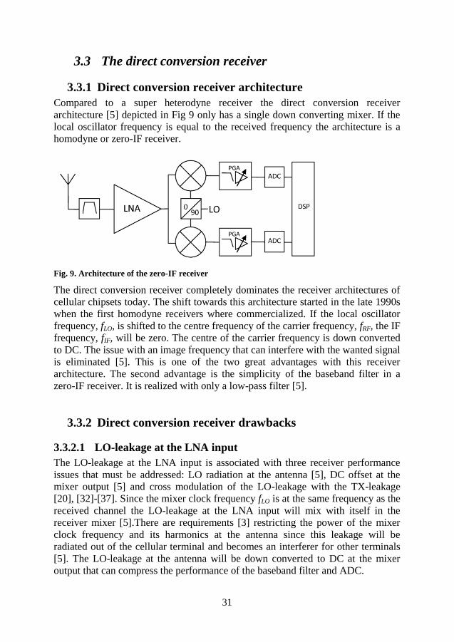
3.3 The direct conversion receiver
3.3.1 Direct conversion receiver architecture
Compared to a super heterodyne receiver the direct conversion receiver
architecture [5] depicted in Fig 9 only has a single down converting mixer. If the
local oscillator frequency is equal to the received frequency the architecture is a
homodyne or zero-IF receiver.
Fig. 9. Architecture of the zero-IF receiver
The direct conversion receiver completely dominates the receiver architectures of
cellular chipsets today. The shift towards this architecture started in the late 1990s
when the first homodyne receivers where commercialized. If the local oscillator
frequency, fLO, is shifted to the centre frequency of the carrier frequency, fRF, the IF
frequency, fIF, will be zero. The centre of the carrier frequency is down converted
to DC. The issue with an image frequency that can interfere with the wanted signal
is eliminated [5]. This is one of the two great advantages with this receiver
architecture. The second advantage is the simplicity of the baseband filter in a
zero-IF receiver. It is realized with only a low-pass filter [5].
3.3.2 Direct conversion receiver drawbacks
3.3.2.1 LO-leakage at the LNA input
The LO-leakage at the LNA input is associated with three receiver performance
issues that must be addressed: LO radiation at the antenna [5], DC offset at the
mixer output [5] and cross modulation of the LO-leakage with the TX-leakage
[20], [32]-[37]. Since the mixer clock frequency fLO is at the same frequency as the
received channel the LO-leakage at the LNA input will mix with itself in the
receiver mixer [5].There are requirements [3] restricting the power of the mixer
clock frequency and its harmonics at the antenna since this leakage will be
radiated out of the cellular terminal and becomes an interferer for other terminals
[5]. The LO-leakage at the antenna will be down converted to DC at the mixer
output that can compress the performance of the baseband filter and ADC.

32
In zero-IF receivers the DC offset at the mixer output has been reduced by running
the receiver voltage controlled oscillator (VCO) at a frequency fVCO that is an even
multiple of the mixer clock frequency fLO. If the clock signal to the mixer is a
square wave the Fourier transform of this signal only contains odd harmonics of
fLO. Leakage at fVCO or at harmonics of fVCO at the LNA input does not result in any
DC offset since the mixer clock signal does not contain any harmonics of fVCO. In
paper I the LO-leakage due to mismatch in the switching stage of the active mixer
is attenuated with a feedback loop around the mixer core.
3.3.2.2 DC-offset at the mixer output One easy way to eliminate the problem with DC-offset would be to AC-couple the
output signal from the mixer [2]. However this is not a feasible architecture since
modulation schemes used for high speed communication, e.g. 64QAM [16]
contain information at low frequencies close to DC. Considering the impedance in
the interface between the mixer and the baseband filter the size of the AC-coupling
capacitor, required not to cause increased BER, is not feasible to integrate on-chip.
The preferred way to reduce the DC-offset is instead to use offset cancellation
techniques [5]. With these techniques the DC-offset is measured and averaged
over time and then subtracted from the output signal. DC-offsets as well as cut-off
frequencies in the baseband filter are reduced by using calibration techniques. In
paper I the mixer DC-offset is attenuated using a feedback loop around the mixer
core.
3.3.2.1 Sensitivity to second order distortion Second order nonlinearities in the zero-IF receiver cause performance degradation
in TDD as well as in FDD systems. In E-GSM the receiver must handle an AM-
modulated interferer at 6MHz offset from fLO. In FDD systems the AM-
modulation of the TX-leakage generates second order distortion from self mixing
[5], second order nonlinearities in the transconductance stage [31], second order
nonlinearity in the switching core devices and cross modulation of the LO-leakage
[20], [32]-[37].
3.3.2.2 Sensitivity to mixer 1/f noise
Since the RF signal is down converted to DC the zero-IF receiver is sensitive to 1/f
noise [5]. The 1/f noise in active mixers with a bipolar switching core is much
lower compared to the 1/f noise in active mixers in CMOS technology. In CMOS
technology the passive mixer architecture is therefore dominating. The mixer in
paper I is designed with a bipolar switching core.

33
3.4 The low-IF receiver
In the low-IF architecture [38], [39] the LO frequency is offset from the RF carrier
frequency in the range of the channel bandwidth [38]. The down conversion to
baseband frequencies can take place in a complex mixer in the digital domain [38]
providing image rejection. A typical low IF receiver architecture is depicted in
Fig. 10.
Fig. 10. Architecture of the low-IF receiver
Since both the wanted signal and the image frequency are present in the input
signal to the ADC the requirements for the ADC in a low-IF receiver are higher
compared to a homodyne receiver. This increases the power consumption of the
ADC. The image power could be significantly higher compared to the wanted
signal. One advantage with this architecture is that the ADC is AC coupled to the
preceding analog part of the receiver. This eliminates the need of DC-offset
compensation. The low-IF receiver is less sensitive to 1/f noise originating from
the mixer since the carrier frequency is not down converted to DC as in the zero-IF
receiver. Especially in active CMOS mixers noise figure degradation due to 1/f
noise is troublesome. Passive CMOS mixers ideally do not suffer from excess 1/f
noise since there is no DC biasing current [40]. Compared with the zero-IF
receiver, the signal processing of the IF-signal that is required after the mixer is
more demanding in a low-IF receiver. In the low-IF receiver image rejection [38],
[39] must be implemented either in the analog or the digital domain. In either way
the image rejection is highly sensitive to mismatch. [38], [39].
Instead of implementing a complex mixer for image suppression in the digital
domain a complex band pass filter could be designed in the analog domain [38].

34
3.5 Receiver architecture summary
The zero-IF receiver architecture is the preferred choice for cellular terminal
receivers even if there are drawbacks with this solution. However, compared to the
calibration required to achieve sufficient image rejection in a low-IF receiver these
drawbacks are easier to circumvent by high performance design of e. g. LNAs and
mixers.

35
CHAPTER 4
4 Process technology and device performance
4.1 Introduction
The digital part of the integrated transceivers is increased for each new circuit
generation. It is common today even to include a microprocessor used in automatic
calibration of the circuit. In these system on chip architectures digital signals, e.g.
harmonics of the digital clock frequency can leak to the LNA input through the
supply lines, electromagnetic coupling or through the substrate [41]-[49]. On-chip
isolation governed by package and process technology is therefore becoming
increasingly important. An increased digital part also means that more digital
devices are switching simultaneously thereby creating more interference [44],
[49]. Digital and analog functions that used to be on different dies are now merged
together. The effectiveness of e.g. triple-well devices [49] is reduced for higher RF
frequencies in new operating bands. For high frequency bands the package
impedance is also higher.
4.2 Process technology
CMOS is the silicon mass production technology of today [14]. This applies to
both cellular transceiver circuits as well as digital circuits. As a result of the high
CMOS volumes the production cost is reduced. For cellular RF circuits in the mid
2000s BiCMOS technology was still competitive. The last technology step in
BiCMOS was the performance enhancement by introduction of the SiGe bipolar
devices [50]. There are several differences between bipolar and CMOS devices
that affect the architecture and design tradeoffs for a transceiver circuit [50]. One
difference is that the bipolar devices have a higher transconductance-to-current
ratio compared to the MOS device. The gm/IC ratio for a bipolar device equals
1/VT. For a MOS device the gm/ID ratio for a long channel device equals 2/(VGS-VT)
and 1/(VGS-VT) for a short channel device [50]. Compared to a bipolar device the
gm/ID of the MOS device decreases when the device bias current increases.
Despite this drawback the fT of CMOS processes is today very high due to device
scaling. The supply voltage is reduced as the gate oxide thickness reduces. This is
a difference compared to bipolar devices that offer high fT with high supply

36
voltage [14]. High voltage devices are an advantage in e.g. power amplifier design
[14]. A second difference comparing bipolar and CMOS technology is the much
higher level of 1/f noise in CMOS. The 1/f noise originates from traps in the
interface between the gate oxide and the silicon that randomly release charges
[52]. The passive mixer [52] is the preferred architecture in CMOS technology
compared to BiCMOS technology where an active mixer with bipolar switching
commonly used. This architecture is used in the mixer presented in paper I. Using
CMOS devices in the switching core increases the 1/f noise.
When the device size is reduced the matching properties is deteriorated. This is an
issue for e.g. differential architectures making it difficult to use the minimum size
devices. For low frequency design device up-scaling is an effective way to
counteract mismatch. This technique is used in the mixer DC feedback loop in
paper I.
The performance of the analog RF part is strongly dependent on the passive
components, i.e. the inductors and capacitors. The Q-value of an on-chip inductor
[41], [48], [51] is one of the key metrics for comparing semiconductor processes.
The noise figure of the LNA with integrated matching presented in paper II is
strongly dependent on the Q-value of the integrated matching inductor.
4.3 Package technology
The package technology evolution has resulted in that the wire-bonded package
type is no longer used for integrated transceivers for cellular terminals. The
inductance of the bond wires was in the range of a few nanohenries. Coupling
between nearby wires as well as supply line noise coupling was an issue in RF
design. The state-of-the art packages today instead use flipped dies mounted on
ball-grid arrays (BGAs) [53]. The total inductance of a connection pin is then
about 200pH, including routing inductance in the flip-chip redistribution layer.
The redistribution layer is the routing interface between the BGA and the pads of
the die. Compared to the coupling between bond wires the coupling between the
balls of the BGA package is negligible since the ball inductance is less than 50pH.
There is however still a significant coupling between wires in the chip
redistribution layer. For a ground connection a low inductance is obtained using
parallel connection of multiple grounds. Passive components as decoupling
capacitors and matching components for LNAs can be placed inside the package
reducing the number of components on the PCB. This is used in the design
presented in paper I requiring two off-chip capacitors. A low package inductance
is desirable since the supply and ground will become more ideal, thereby relaxing
the requirement on power supply rejection ratio (PSRR). Low impedance paths to
ground are important for isolation, e.g. for the effectiveness of shunting an
undesired signal to ground. This is used in the multiband LNA in paper II for
increasing the isolation between different RF inputs. To reduce the coupling
careful planning and routing is required regarding placement of signals in the die
pad ring and BGA package. Supply connections with low package impedances

37
make it possible to use architectures that would otherwise have been hard to
implement, e.g. the multiband single ended LNA presented in paper II.
4.4 Substrate coupling
Compared to differential architectures single ended architectures are more
sensitive to substrate noise and interference and require more careful substrate
interference robust [45] design. Substrate noise is caused by different sources
[41] - [43]. These sources can be divided into internal sources and external sources
referring to how the noise couples to the substrate [42]. The internal noise is
generated when e.g. digital gates are switched [44] and the noise is coupled
through the parasitic capacitances of the active devices, wells and interconnects.
The external noise is created when the noise path from the digital to analog part of
the die goes through the power domain network. The switching gates introduce
noise on the supply lines. This noise is then coupled back to the sensitive analog
part through substrate contacts in the analog domain connected to supply and
ground [41], [42]. Depending on the package inductances and decoupling
capacitors of the power distribution network the external noise can be dominating.
Low package inductance is therefore important to reduce the external coupling.
[41].The internal noise becomes more important when the packages inductances
are very small. Three mechanisms govern substrate interference: injection,
propagation and reception [42]. Noise can be injected into the substrate in three
ways [42]
1. Substrate coupling through capacitances [41], [42], [47]
The source and drain of each MOS devices is coupled to the substrate through a
depletion capacitance. Depletion capacitance coupling is also an issue in bipolar
process technology [46]. Interconnect lines also have a capacitance to the substrate
[48]. If the interconnect carries a rail to rail digital signal and the length of the wire
is long the injected substrate noise can be substantial. Bond pads have a significant
capacitance to ground as well. If e.g. a digital I/O signal is connected to the pad
noise can be injected into the substrate.
2. Injection through substrate contacts [41], [42]
NMOS and PMOS devices have either p+ or n+ diffusions close to the devices to
set the potential of the bulk to either VCC or GND. The source and bulk terminal
are usually connected together. The supply and ground on the die are connected to
ideal ground through the series inductance and resistance of the package resulting
in supply and ground bounce when e.g. a digital transition occurs in the circuit.
Noise is thereby injected into the substrate through the substrate contacts
connected to the noisy supply and ground.
3. Impact ionization currents [41], [42]
Electron-hole pairs are generated by high electric filed in the drain. The holes will
diffuse down to the substrate.
Noise propagation in the substrate depends on the substrate type. Three types of
substrates are used in CMOS processes [43]

38
1. Epitaxial substrates
The wafer consists of a high-resistivity thin layer on top of a low
resistivity bulk. The majority of the substrate noise propagates in the
highly doped bulk. Due to the low resistivity the bulk can be regarded as
one node. The purpose of this type of substrate is to prevent latch-up.
2. Non-epitaxial substrates
The wafer consists of only high resistivity bulk. The substrate current is
more uniformly distributed. Increasing the distance between an interfering
block and a noise sensitive block helps to improve the isolation with this
type of substrate.
3. Silicon-on-insulator (SOI) substrates
The devices are fabricated in silicon islands isolated from the substrate by
a buried oxide layer. These processes have a much higher isolation
compared to the two other types.
The same effects that cause noise injection also govern noise reception. Substrate
injection and reception can be reduced using triple-well devices. The benefit is
however strongly dependent on the operating frequency as well as the package
impedance of the well connection [49]. Substrate propagation can be reduced
using guard rings. Guard rings are more efficient in a lightly doped process [42].
The substrate noise is attenuated by sinking the noise current to a low impedance
ground. The effect of the ring is dependent on the inductance of the supply
connection [49]. Other substrate propagation reduction techniques are trenches, N-
wells to break the channel stop and deep N-wells below the interfering block [42].
Reduction of noise reception can be achieved by using differential structures [42]
since substrate noise can be regarded as common mode noise. On-chip decoupling
is efficient to prevent noise from reaching the supply lines [41].
4.5 Basic equations for the MOS and bipolar transistors
4.5.1 Introduction
The design presented in paper I is single ended LNA and active mixer in BiCMOS
technology. The LNA presented in paper II is designed in CMOS technology. The
fundamental transistor equations for both CMOS and bipolar devices are provided
in section 4.5.2 and 4.5.3 respectively.
4.5.2 MOS transistor equations
In the saturation region (21) applies for the relation between the drain current ID,
the threshold voltage Vt, the gate-source voltage VGS and the drain-source voltage
VDS [54], [55].
)1()(2
2'
DStGSD VVVL
WkI (21)

39
The parameter k´ defined in (22) is the product of the electron mobility n and the
gate oxide capacitance per unit area Cox.
ox
oxnoxn
tCk
'
(22)
The parameters ox and tox are the permittivity and thickness of the gate oxide
respectively [54], [55]. The parameter in (23) is defined by the output resistance
and drain current of the NMOS [54], [55]. With shrinking device dimensions the
output resistance is decreased which is not beneficial for analog design.
Dout Ir
1 (23)
The small signal transconductance [54], [55] is defined in (24).
)1)(('
DStGS
GS
Dm VVV
L
Wk
V
Ig
(24)
If VDS<<1 the transconductance is approximated by (25).
DtGSm IL
WkVV
L
Wkg '' 2)( (25)
The transconductance gm is proportional to W/L times the overdrive voltage, Vov
[54], [55] defined in (26).
tGSov VVV (26)
Decreasing the channel length and the thickness of the gate oxide increases the
transconductance gm. The MOS transistor cut-off frequency T [54], [55] given by
(27) can be used to calculate the expected transconductance of e.g. an LNA.
gs
mT
C
g (27)
A thorough description of MOS device parameters is provided in [54], [55].
4.5.3 Bipolar transistor equations
For the bipolar transistor in the forward-active region (28) applies for the relation
between the collector current IC, the base-emitter voltage, VBE, the saturation
current, IS and the collector-emitter voltage, VCE [55].

40
T
BE
A
CESC
V
V
V
VII exp)1( (28)
The parameter VA is the early voltage [55] defining the variation of IC with VCE.
The threshold voltage is denoted VT. The small signal transconductance, gm, is
given by (29).
kT
qI
V
Ig C
BE
Cm
(29)
The output resistance [55], ro, is defined in (30).
C
A
C
CEo
I
V
I
Vr
(30)
The bipolar transistor cut-off frequency [55], T, is given by (31)
CC
gmT
(31)
The emitter-base junction depletion capacitance is denoted C and C is the
collector-base junction capacitance. A detailed description of bipolar device
parameters is provided in [55].

41
CHAPTER 5
5 LNA architectures
5.1 Introduction
The intention of the LNA is to relax the noise requirements of the mixer, baseband
amplifier and the ADC. Selectivity, i.e. to attenuate undesired signals is a desired
property. In multi mode terminals with integrated WLAN a WLAN transmit signal
at 5.8GHz leaking into the cellular LNA will be down converted by third harmonic
downconversion [56], thereby corresponding to an in-band interferer at 1933MHz.
A narrow band LNA as described in paper II will attenuate this interferer. Wide
band input matching LNAs, e.g. resistive feedback [57], [58] and common-gate
[59]-[62] LNAs do not provide any selectivity but on the other hand ideally do not
require any external matching components. In order for the receiver sensitivity to
be maximized the LNA should preferably have a low noise figure as in
combination with a high gain. In a FDD system the compression point of the
receiver must be high enough in order to not compress on the own transmit signal.
In a TDD system as E-GSM the compression point is determined by a blocking
signal at 3MHz distance from the desired signal. The third order linearity should
be high enough not to create intermodulation products. The second order
nonlinearity is not important since AC-coupling of the LNA output to the mixer
input attenuates low-frequency IM2 products. The current consumption of the LNA
is determined by the compression point requirement. In paper II the current
consumption is reduced when the terminal is close to the base station, i.e. the own
TX signal is weak. In multi band LNA architectures as in Fig. 1 the isolation
between the LNAs is important. The TX signal can leak through the rather poor
isolation of the antenna switch to the input of an unused LNA for certain
frequency bands where the TX frequency overlaps the RX frequency of the turned
off LNA. If the LNA isolation is not adequate this leakage path could deteriorate
the TX to RX isolation given by the duplexer. Programmable input RF switches
with both high isolation and low series resistance are presented in paper II. The
bandwidth of the input matching of the narrow band LNA must cover the targeted
frequency band with a sufficient margin to handle the production spread.
42
5.2 Single ended versus differential LNA architectures
The differential LNA is the dominating architecture in cellular receivers. This
topology offers advantages compared to its single-ended counterpart, e.g. built-in
PSRR and rejection of common mode interferers in the ground and substrate.
However, as the number of supported frequency bands increase as well as support
for e.g. Wi-Fi, Bluetooth and GPS becomes mandatory, the differential LNA
architecture becomes less attractive due to the additional RF input pin that
increases the package size. The LNAs presented in paper I and II are both single
ended. Routing of the RF input signal on the PCB then becomes less troublesome.
Single ended LNAs suffer from other drawbacks though. Interferers in the supply
ground and substrate are only suppressed in the differential LNA resulting in
increased design requirements for the single ended architecture. Decoupling of the
supply, both on the die and on the PCB, is important to reduce interference.
Harmonics of the digital clock signal leaking to the LNA input require more
careful design if a single ended LNA is used [70]. With the package technology
available today, e.g. flip-chip and BGA [53], the ground impedance is much lower
compared to wire-bonded packages. This is beneficial for single ended LNAs that
are more sensitive to interferers and noise on the die ground.
5.3 LNA architectures in CMOS technology
5.3.1 Common-source LNA with inductive degeneration
5.3.1.1 Introduction
Compared to the common-gate (CG) architecture [59]-[62], [72], [73] the
common-source (CS) LNA with inductive degeneration [70]-[73] is the
architecture can give the lowest noise figure (NF) [72]. With an operating
frequency 0 and a transit frequency T the NF of the CG LNA is constant with
respect to 0/T while the NF of the CS LNA is linear proportional to 0/T.
[72].The LNA has narrow band input matching and is commonly matched with an
external inductor in series with the gate. The Q-value of the external inductor has a
large impact on the LNA noise figure. The multiband LNA presented in paper I
has a CS architecture but has an on-chip inductor.
5.3.1.2 Input matching
The inductively source degenerated MOS LNA has the advantage that it creates a
real part of the input impedance without adding a resistor [74]. In Fig. 11 Cgs is the
gate-source capacitance of the LNA input device with transconductance gm.

43
Fig. 11. Architecture of the CS LNA with inductive degeneration
From the small signal model the current through the source inductor Ls is given in
(32) by the sum of the source current and the input current at the gate iin.
gs
inminsgminLsC
igivvgiis
1)( (32)
The voltage sLv across the source inductor is then given by (33).
)()1
(gs
smsin
gs
inminsLsLC
LgsLi
sCigisLisLv
ss (33)
The input impedance Zin [74] is defined by (34)
gs
ss
gs
m
in
CL
in
inin
sCsLL
C
g
i
vv
i
vZ
gss 1
(34)
A real impedance is created by generating a current proportional to 1/s (the source
current in the MOS device) and pushing it into an impedance proportional to s (the
source inductor Ls). Replacing s by j gives Zin() in (35).
)1
(gs
ss
gs
min
CLjL
C
gZ
(35)
The source inductor Ls lowers the LNA gain through negative feedback thereby
improving the linearity. The inductor also introduces a real part to the input
impedance [74]. The real impedance is used to match the LNA to the 50 source
impedance, Rs. The real part of the input impedance, Rin, is given in (36).
s
gs
minin L
C
gZR )Re( (36)

44
If Ls is chosen, gm and Cgs can be calculated to give the required Rin (50). In order
to cancel the imaginary part of Zin an inductor Lg is connected in series with the
gate, The imaginary part of Zin is the defined by (37).
01
)()Im( gs
gsinC
LLZ
(37)
In practice the expressions for the real and imaginary part of the input impedance
derived in (36) and (37) are only valid for the CMOS LNA input device together
with the source inductor standalone. In a real design there are capacitive parasitic
from the pads and ESD-diodes and from the wiring from pad to gate of the LNA
input device. There is also an inductive parasitic from the pad to the gate of the
input device. The package adds both inductive and capacitive parasitics. When
these parasitics are added to the design the expression for Zin becomes more
complex. Usually one more component besides the series inductor Lg is required to
match the LNA to the source impedance. Accurate modeling of the parasitics both
on the die and in the package using an electromagnetic simulator is necessary in
order to determine the external matching components.
5.3.1.3 Input matching bandwidth
Reviewing (34), a series resonance circuit [17] is formed by the input source
resistance Rs, the matching series inductor Lg, the real part of the LNA input
impedance, Rin, Cgs and Ls as depicted in Fig. 12. At resonance the voltage across
Cgs will be Qin times larger than the input voltage vin.
Fig. 12. Model for input matching Q-value calculation
With the input voltage vin defined after the source impedance Rs (38) applies at
resonance.
)(
10
gsgs LLC (38)
The LNA input voltage vin is defined by (39)
ininin Riv (39)

45
The gate-source voltage vgs is then given by (40).
gs
ingsgs
gs
ingsC
iLLC
Civ )(
1
0
(40)
The voltage ratio vgs/vin is equal to Qin and is defined by (41).
in
ings
sg
ings
gsgs
in
gsQ
RC
LL
RCLLC
v
v
11)( (41)
At the resonance frequency 0 the voltage across Cgs will therefore be Qin times
the input voltage vin. The drain signal current of the input device is given by (42).
ininmgsmLNAd Qvgvgi _ (42)
Including the source resistor Rs in the Q-value calculation relates the drain current
to the source voltage vs.
ssmgsmLNAd Qvgvgi _ (43)
The overall transconductance from the source input to the drain output, Gm_tot_LNA,
is given by (44).
s
gs
ms
gs
sg
msm
s
LNAd
LNAtotm
LC
gR
C
LL
gQgv
iG
_
__ (44)
The overall transconductance Gm_tot_LNA is Qs times larger than the MOS device gm
since the gate-source voltage is Qs times larger than the input voltage vs. If the
width, W, of the input device decreases with constant bias current, gm and Cgs
decreases. To keep the resonance frequency 0 constant the inductance has to be
increased by the same factor that Cgs was decreased by. With fixed drain current Id
and using (25) halving W and keeping L makes 12 21 mm gg and 212 gsgs cc .
The Q-value of the input matching with the width W1 is defined in (45) as Qs1.
)(1
11
1
11
1
gs
sms
gs
sg
sC
LgR
C
LLQ
(45)
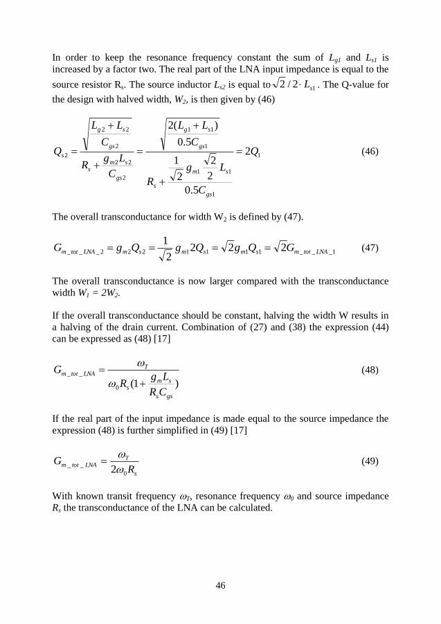
46
In order to keep the resonance frequency constant the sum of Lg1 and Ls1 is
increased by a factor two. The real part of the LNA input impedance is equal to the
source resistor Rs. The source inductor Ls2 is equal to 12/2 sL . The Q-value for
the design with halved width, W2, is then given by (46)
1
1
11
1
11
2
22
2
22
2 2
5.0
2
2
2
1
5.0
)(2
Q
C
Lg
R
C
LL
C
LgR
C
LL
Q
gs
sm
s
gs
sg
gs
sms
gs
sg
s
(46)
The overall transconductance for width W2 is defined by (47).
1___1111222___ 2222
1LNAtotmsmsmsmLNAtotm GQgQgQgG (47)
The overall transconductance is now larger compared with the transconductance
width W1 = 2W2.
If the overall transconductance should be constant, halving the width W results in
a halving of the drain current. Combination of (27) and (38) the expression (44)
can be expressed as (48) [17]
)1(0
__
gss
sms
TLNAtotm
CR
LgR
G
(48)
If the real part of the input impedance is made equal to the source impedance the
expression (48) is further simplified in (49) [17]
s
TLNAtotm
RG
0
__2
(49)
With known transit frequency T, resonance frequency 0 and source impedance
Rs the transconductance of the LNA can be calculated.

47
In a real design it is of high importance for the bandwidth of the LNA to cover the
dedicated frequency band with sufficient margin. Semiconductor process
variations as well as changes in supply voltage and temperature will cause the
input matching to drift. The Q-value of the input matching must therefore not be
too high. The multiband LNA in paper II is scaled to cover the frequency bands
with a margin. Capacitive parasitics to ground from the pad to the gate of the LNA
input device will reduce the bandwidth of the matching. These parasitics should be
minimized by not using a too wide input wire and route it using a high metal layer.
The required input matching Q-value determines the gate-source capacitance, Cgs.
By differentiating the total stored charge in the MOS channel, QT, to VGS, Cgs is
given by (50) [17].
ox
GS
Tgs WLC
V
QC
3
2
(50)
The transconductance gm is defined using (51) together with a desired value for
Gm_tot_LNA, The expression for the real part of the input impedance (36) then gives
the value of the source inductor Ls. The required drain current, ID, is defined by
(21). In practice however a matching network of two external components can be
used. This is often necessary due to large capacitive parasitics for the input signal
both on the die and in the package.
The LNA is can then no longer be matched with only one series inductor Lg and
Re(Zin) in (36) does not have to be equal to the source impedance. This is can be
used for noise optimization.
5.3.1.4 Noise model for the CS LNA with inductive degeneration
A noise model [55] for the CS-stage LNA with inductive degeneration inductor Ls
and a series matching inductor Lg is depicted in Fig. 13.
Fig. 13. Noise model for the CS LNA with inductive degeneration

48
The noise figure of the LNA will depend on the following noise sources [55].
Gate resistance
The gate wiring in polysilicon will add resistance in series with the gate [55]. This
noise contribution can be minimized by increasing the number of fingers in the
input device and contacting the gate at both ends. The gate resistance is
represented by the 2
_ grv noise voltage source.
The series resistance of the matching inductor Lg
The matching inductor has a significant series resistance. The inductor resistance
is represented by the gLrv2
_ noise voltage source. The LNA presented in paper II
has a significant noise contribution from Lg since the Q-value of the on-chip
inductor is limited.
The series resistance of the source inductor Ls
The noise from the source inductor is represented by the sLrv2
_ noise voltage
source.
Channel noise
The channel noise [55] 2
di in (51) is the dominant noise in CMOS technology at
RF-frequencies. It is affected by device size (W/L) and biasing.
fgkTi dd 0
2 4 (51)
The parameter gd0 is the conductance with regard to VDS with VDS=0V [55]. The
parameter equals 2/3 for a long channel device [55]. For a short channel device
is larger. The channel noise is represented by the 2
di noise current source
Induced gate noise
Fluctuations in the channel charge will induce a physical current in the gate due to
capacitive coupling. When the channel is inverted the following (52) applies for
the induced gate noise [55]
fgkTi gg 42 (52)
The parameter gg is defined by (53) [55].
0
22
0
5 d
gs
gg
Cg
(53)

49
The gate noise coefficient equals 4/3 for a long channel device [55]. The
parameter gd0 is the conductance with regard to VDS with VDS=0V [55]. With
VDS=0V the device is in the triode region, i.e. (54) applies for the drain current
[55].
)2
)((2
2'
DSDStGSD
VVVV
L
WkI (54)
The conductance gd0 is then given by (55) [55].
)(2
'
00 tGSVDS
DS
Dd VV
L
Wk
V
Ig
(55)
The induced gate noise is partially correlated with the channel noise current id
because it is generated by the channel noise current itself [55].
Flicker noise (1/f-noise)
The 1/f noise [52], [55] is caused by traps at the interface between the channel and
the gate oxide. These traps randomly capture and release carriers. For the design of
the LNA the corner frequency of the 1/f-noise is far below the operational
frequency. If the LNA is connected to mixer by an AC-coupling capacitor or a
balun, the 1/f noise of the LNA can be neglected. The 1/f noise contribution is
defined in (56).
ff
IKI
a
Df 2
/1 (56)
The parameter K is a device constant and the parameter a is constant between 0.5
and 2 [55]. An advantage of the CS stage LNA is that the resistive input
impedance is noiseless [75]. The noise factor of the CS architecture is given by
(57).
52)1(
51
11
22
2
0 cQQ
FT
(57)
In (58) c, , and are bias dependent parameters [55], [75], [76]. An optimal Q-
value for the input matching exists where the noise figure is minimized [70], [76].
A high Q reduces the contribution of channel noise while the gate noise is
increased [76].
5.3.1.5 CS stage LNA third order linearity
Compared to the collector current of a bipolar device which has an exponential
dependency of the input voltage [55], the MOS drain current ideally follows a
square law dependency on the input voltage. Assuming that VDS<<1 in (21) the

50
relation between the drain current and the gate-source voltage VGS is expressed in
as (58).
2'
)(2
tGSDC VVL
WkI (58)
The large signal drain current ID(t) as a function of bias voltage VGS and a small
signal voltage vgs is given by (59).
)(2
)()()()( 2'
' tvL
WktvVV
L
WkItIItI gsgstGSDCdDCD (59)
From (60) it follows that there is no third order term present. However, adding the
second order effect of mobility degradation [55] changes the relation between ID
and VGS as defined in (60)
)(1
)(
2
2'
tGS
tGSDC
VV
VV
L
WkI
(60)
The variable is a process technology dependent parameter [55]. After a Taylor
expansion of the expression in (60) for ID(t) versus VGS and vgs, the third order
intercept point IP3 is given by (61) [55].
3
)(83_
tGSIPgs
VVv
(61)
The intercept point is referred to vgs of the MOS device. To refer it back to the
input the relation between vgs and the Q-value of the matching net is utilized in
(62).
in
tGSIPin
Q
VVv
1
3
)(83_
(62)
To design an LNA with high IP3 the Q-value of the input matching net should be
low and the gate overdrive voltage VGS-Vt should be high.
5.3.2 CS-stage LNA with integrated balun
A differential mixer is commonly used in order to suppress second order distortion
[4]. In combination with a single ended LNA, single ended to differential
conversion is required. For this conversion an on-chip balun can be used. The
advantage of the balun is that it also provides voltage gain. This architecture is
used in paper II and is depicted in Fig.14. A tuning capacitor is connected at the
balun primary side to alter the balun resonance frequency.

51
Fig. 14. CS LNA with inductive degeneration and integrated balun
The voltage gain from the input port to the differential balun output, Gv, is defined
in (63).
balunvbaluninLNAtotmv GZGG ____ (63)
Gm_tot_LNA is the overall transconductance from the input port to the output of the
cascode. Gv_balun is the voltage gain of the balun. Zin_balun is the impedance seen
looking into the balun and tuning capacitor from the LNA cascode output. For a
certain required voltage gain the balun is useful for reducing the current
consumption of the LNA. From (63) it follows that Gm_tot can be reduced if either
Zin_balun or Gv_balun are increased.
5.3.3 The common-gate architecture LNA
At operating frequencies that are low in comparison with T of the MOS input
device the noise figure of the common-gate LNA is higher compared to the
common-source architecture [60]. Compared to the CS architecture, the CG LNA
offers higher linearity and wider input matching [60], [72]. For higher frequencies
the noise figure of the LNA is lower for the CG LNA compared to the CS
topology since compared to the CS architecture the noise figure of the CG LNA is
independent of the operating frequency [60], [72], [73]. A common CG LNA
topology is depicted in Fig. 15 including the parasitic gate-source capacitance of
the input MOS together with the input pad capacitance Cpad. All parasitic
capacitance, i.e. from package, pad and routing are included in Cpad.

52
Fig. 15. Architecture of the CG LNA including parasitics
A parallel resonant network is used to match the input impedance of the transistor
(1/gm) to the source impedance (50Ω) [60].
s
gspadminsL
CCsgY1
)( (64)
If the operational frequency of the LNA is low, i.e. <<T, this is not necessary
and the input impedance of the LNA is simple given by the inverse of the
transconductance. With gmRs = 1 the noise factor F is defined by (65) [60].
1F (65)
The parameters and are empirical process- and bias-dependent parameters
[60], [73].
5.3.3.1 Common-gate LNA gm-boosting
One way of improving the noise figure of the CG LNA is to use the gm-boosting
technique [60], [73] depicted in Fig. 16. In a CG LNA the input matching
requirement (66) limits the achievable noise figure to (65).
smieffm RgG /1, (66)
If the effective transconductance of the stage looking into the source terminal is
denoted Gm,eff and the and gmi represents the small signal transconductance of the
MOS device, the noise factor can be expressed in detail as (67) [60].
2
,
1
11
seffm
s
mi
RG
R
gF
(67)

53
The effective transconductance is increased by inserting an inverting amplifier
between the source and gate terminal [60] as depicted in Fig. 16.
Fig. 16. Common-gate LNA with gm-boosting feedback
The effective transconductance [60] is now defined by (68).
mieffm gAG )1(, (68)
The increased transconductance, Gm,eff, of the CG LNA improves both the noise
factor as well as the power consumption of the common-gate architecture [60].
With the gm-boosting by the feedback with gain A, the noise factor of the CG LNA
[60] is given by (69).
)1(
11
1
1
11
2
ARgA
R
gF
smi
s
miboostgm
(69)
In (69) the condition for the input matching defined by (70) has been used.
mieffms gAGR 1/1 , (70)
From (69) the contribution to the noise factor from / is reduced by a factor
(1+A) with the gm-boosting technique. Using (70) gives smi RAg 1/1 . With a
reduced intrinsic transconductance gmi, the current consumption is thereby also
reduced. The expression (69) is valid only if the amplifying stage does not add any
noise itself [60].
5.3.3.2 Capacitive cross coupling gm-boosting
One way to realize the gm-boosting amplifier in Fig. 16 is depicted in Fig. 17
outlining a differential common-gate LNA with capacitive cross-coupling. [60],
[61], [73]. A passive implementation is advantageous since the amplifier should
add as little noise as possible.

54
Fig. 17. Differential CG LNA with capacitive cross coupling
The gain, A, of the inverting amplifier is now given by a capacitive voltage
division of the input signal with cross capacitor value denoted Cc [60], [61] as
defined in (71)
gsc
c
CC
CA
(71)
If Cc Cgs the gain of the inverting amplifier equals approximately 1 and the noise
factor of the capacitor cross-coupled LNA is given by (72) [60], [61]
21F (72)
Using capacitive cross coupling the noise factor is reduced, the effective
transconductance is increased and the current consumption is decreased.
5.3.4 The resistive feedback CMOS LNA
The resistive feedback CMOS LNA depicted in Fig. 18 has a wide-band input
impedance [17], [57] defined by (73)
miin gZ /1 (73)

55
Fig. 18. CS LNA with resistive feedback
A wideband input matching is desired in certain application such as ultra wide-
band receivers. In cellular multi-band receivers a duplexer (in FDD systems) or a
SAW-filter (in TDD systems) precedes each RF input. A wideband LNA could
replace several narrow-band LNAs but due to the necessity of the band specific
external filters the switches are required to connect the wide-band LNA to the
desired filter.
Compared to the CS LNA the resistive feedback LNA does not require any
matching components. The voltage gain of resistive feedback LNA [17], [57] is
given by (74).
RgVVA miXYv 1/ (74)
If the input is matched to the source resistance Rs the noise figure is typically
higher than 3dB [57] which is not low enough for cellular applications. If noise
cancellation [57 is applied to this topology the performance can be significantly
improved.
5.4 Noise cancelation
5.4.1 Introduction
The principle of noise cancelation [57], [76], [77] is depicted in Fig.19 [57]. It can
be applied to other architectures than the resistive feedback LNA as well.
Fig. 19. Block description of noise cancelation

56
Input matching to the source impedance Rs is provided through the block
“Matching Amplifier Stage”. The noise and wanted signal at the source is also
measured and amplified by the block “Voltage-sensing Amplifier Stage”. The
wanted signal and noise from these two stages are the combined in order to cancel
the noise from the matching device and add the two desired signals.
5.4.2 Noise cancelation with resistive feedback LNA
The noise canceling concept applied to a resistive feedback LNA is depicted in
Fig. 20 [57] outlining the matching amplifier stage, the voltage-sensing amplifier
with gain –Av and the combining network in Fig. 19 realized as an adder. The
input matching device creates a noise current In,i. A noise current (Rs, gmi)In,I
will flow as depicted through the feedback resistor R and the source resistor Rs.
The parameter depends on the relation between gmi and Rs [57]. The noise
voltage at node X and Y will have the same phase [57]. The wanted signal at the
same node will have the opposite phase as the input device inverts the phase [57].
The phase relation between the wanted signal and the noise voltage at the two
nodes X and Y is the base of the noise cancelation technique. The noise and signal
at node X is amplified by the amplifier with gain –Av. For a certain voltage gain of
the amplifier the noise from the input device will cancel at the output node Vout.
The wanted signal will be twice as high at the output compared to the signal level
at node Y.
Fig. 20. CS LNA with resistive feedback and noise cancelation
The noise current (Rs, gmi)In,I flowing through R and Rs will create noise
voltages at nodes X and Y [57] defined by (75) and (76)
sininX RIV ,,, (75)
)(,,, RRIV sininY (76)
At the output after the adder the output noise voltage is then given by (77)

57
)(,,,,,,, svsinvinXinYinout RARRIAVVV (77)
Solving (77) for 0,, inoutV then gives the amplifier gain for cancellation, Av,c
given by (78)
scv RRA /1, (78)
Denoting the voltage gain of the complete noise canceling amplifier AVF,c and
setting the input impedance to Rs gives the amplifier gain in (79).
ssmicvmiXoutcVF RRRRRgARgVVA /2/1/ ,, (79)
The noise from the feedback resistor R and the amplifier with gain –Av is not
canceled. An implementation of the noise cancelling architecture is depicted in
Fig. 21. The amplifier and adder are implemented in the same stage [57]. The
amplifier with gain –Av is formed by the lower NMOS device with
transconductance gm2 and the load defined by the upper NMOS device with
transconductance gm3. The gain Av is given by (80).
32 / mmv ggA (80)
Fig. 21. Implementation of CS LNA with resistive feedback and noise cancelation
The total voltage gain, AVF, is given by the addition of the output voltages from the
resistive feedback input stage and the output voltage of the amplifier with gain –Av
[57].
32 /1 mmSmiVF ggRgA (81)

58
In practice total noise cancellation only occurs at DC for the amplifier voltage gain
Av = Av, c [57]. For high frequencies the parasitic capacitance CIN to ground at the
input node X in Fig. 20 and 21 will degrade the noise performance since the noise
voltages at node X and Y are affected differently when the frequency increases
[57]. Minimizing the input capacitance CIN is therefore important. One way of
reducing CIN is to use a semiconductor process with high fT or to use a cascode at
the input stage. Package parasitics at the RF input also increases CIN. The noise
cancelling concept can also be utilized for distortion canceling [57], [77]. If a
differential input is desired, an architecture with two single-ended stages can be
used [58]. This topology is then connected to a duplexer with differential output.
Typically the differential duplexer has an output impedance of 100 to 200 Ω.
Higher input impedance of the LNA increases the voltage gain measured from the
input port of the duplexer. If the duplexer has an input impedance of Zin_dupl and an
output impedance of Zout_dupl the impedance transformation will give a voltage gain
ofduplinduploutduplV ZZG ___ / . A resistive feedback LNA with noise
cancellation does not have a noise figure as low as a CS LNA with inductive
degeneration. The voltage gain is defined by the noise canceling criteria and is
therefore limited [57, 58].
5.4.1 Noise cancelation with combination of CG- and CS stage
In a common cellular receiver a mixer with differential RF input is used in order to
reduce second order distortion [4]. The architecture outlined in Fig. 22 is a
combination of a CG-stage and a CS-stage that at the same time provides both
noise cancellation and a single-ended input to balanced output conversion [76].
The architecture also provides simultaneous distortion cancelling [76]. Due to the
CG-stage input the architecture has wideband input matching. The design does not
require any balun. It is also not possible to design an on-chip balun that can be
tuned across the entire bandwidth of the CG-stage.

59
Fig. 22. Noise cancelation with combination of CS- and CG stage
To have a balanced balun output at node Vout in Fig. 22 the gain of the CS-stage
should be equal to the gain of the CG-stage but have opposite phase. A CG stage
with a noise source inI , in parallel with the drain current is depicted in Fig. 23. The
input current ini is the same as the current through the load resistor, RCGi [76]. The
input current is given by (82).
CG
CGvin
CG
CGout
RCGinR
Av
R
vii
,, (82)
The input impedance of the CG stage [76] is then defined by (83).
CGv
CG
in
inCGin
A
R
i
vR
,
, (83)

60
Fig. 23. CS-stage with noise source In,i
For a CG-stage the input impedance equals mg/1 and the voltage gain is given by
CGmCGv RgA , . If the input is matched to the source resistance sR , i.e.
sCGin RR , (84) applies [76].
s
CG
CGin
CGCGv
R
R
R
RA
,
, (84)
For the architecture in Fig. 22 to have a balanced output the gain of the common-
source stage should be equal to the gain of the common-gate stage but have a 180
degrees phase as given by (85)
sCGCGvCSv RRAA /,, (85)
In Fig. 22 and 23 the noise of the input CG-device is represented by a noise
current source inI , . The noise source generates two noise voltages, one at the input
node and one at the output node. These two noise sources are correlated but have a
180 degrees phase difference. The noise voltage source at the input is given by
(86) [76].
sininn RIv ,, (86)
The noise voltage at the output is given by (87) [76].
CGinCGn RIv ,, (87)

61
The scaling factor is defined by the voltage division between the input resistance
of the CG-stage, CGinR , , and the source resistance sR [76].
sCGin
CGin
RR
R
,
, (88)
When the gain of the CS stage is equal to the inverse of the gain of the CG stage,
noise cancelling of the CG-stage noise at the differential output outV will occur
since the noise at the CG- and CS stage output will have equal magnitude and
phase [76]. The overall voltage gain is given by (89).
CSmCSCGmCGv RgRgA (89)
It is possible to achieve a significant improvement in noise figure optimizing the
relation between the transconductance and load resistor of the CG-stage and CS-
stage [76]. If the CS transistor is scaled up to be n times larger than the CG
transistor and the voltage gain of the stages are still equal, i.e. CGvCSv AA ,, , the
following applies: mCGmCS gng
and nRR CGCS / . The noise figure will
decrease with increased scaling factor n [76].

62
CHAPTER 6
6 Mixer architectures
6.1 Introduction
The mixer architecture in cellular zero-IF receivers is either active [4], [17], [78]-
[81] or passive [4], [17]. The double balanced mixer [4], [17] is the dominating
topology regardless of the whether the mixer architecture is active or passive. The
key metrics of the mixer are:
- conversion gain
- noise figure
- port isolation
- third order linearity, i.e. IIP3
- second order linearity, i.e. IIP2
- power consumption
- harmonic rejection, i.e. conversion gain for harmonics of fLO
Harmonic rejection [82] is an increasingly important parameter in multi standard
terminals supporting, i.e. Wi-Fi. Harmonic down conversion can also be
counteracted by using narrow band LNA input matching in combination with
narrow band baluns as described in paper II. Double balanced architectures have
been preferred compared to single balanced topologies since these have built in
suppression of common-mode signals, i.e. IM2 products from the RF port as well
as suppression of noise from the LO side. If a balanced LNA is used there is no
need for an on-chip balun that is required with a single-ended LNA. However,
even if a single balanced mixer has drawbacks its performance can be significantly
increased using the technique described in paper 1. The IIP2 and DC-offset of this

63
mixer is from Monte Carlo simulations [83] sufficient for use in a WCDMA
system.
6.2 Active mixers
6.2.1 Introduction
In BiCMOS technology the active mixer architecture [4], [17], [78]-[81]
dominates over its passive counterpart implemented using only MOS devices. The
CMOS part of BiCMOS semiconductor processes is usually a generation behind
the CMOS only processes available at the same time. In BiCMOS technology the
mixer switching core is implemented with bipolar devices as in paper I in order to
reduce the 1/f noise. This is the main concern in active mixers designed with only
CMOS devices for zero-IF receivers [84]-[87]. The active mixer provides
conversion gain while the passive mixer topology results in a loss [4]. This relaxes
the gain requirement of the LNA in an architecture with an active mixer. The
transconductance stage is usually implemented with a MOS device as in the design
presented in paper I since for a given tail current the third order nonlinearity will
be lower for a MOS device compared to a bipolar transistor. The 1/f noise of the
MOS transconductance stage will be up-converted by the switching pair and will
not fall within the baseband frequencies. The active mixer also provides isolation
between the I- and Q branches. This is an issue that must be addressed in passive
mixer implementations using e.g. a 4-phase clock [87]. Since there is no DC-
current in the passive mixer the DC-voltage offset in the passive mixer is much
lower compared with the active mixer.
6.2.2 Single-balanced active mixer
6.2.2.1 Introduction
The single balanced active mixer depicted in Fig. 24 has an NMOS
transconductance stage and a bipolar switching core as in the design presented in
paper I. The mixer load is defined by the resistor RL and the filtering capacitors CL
and CL_diff. The RF signal is single-balanced eliminating the need of either a
balanced LNA or single-ended to balanced conversion in e.g. an on-chip balun if a
single-ended LNA is used. This is the main advantage of the single-balanced
mixer. There are however also important drawbacks with this topology. The mixer
is sensitive to noise from the LO driver compared to the double-balanced topology
[4]. The LO signals do not cancel at the differential output as for the double
balanced mixer [4]. This is not an issue in a zero-IF receiver due to the low-pass
filter at the mixer output. Another drawback is that the single balanced mixer lacks
the built-in suppression of LO to RF leakage that is present in the double balanced
counterpart. If the mixer switching core has mismatch the LO-leakage to the RF
input will increase. In a FDD system with a TX leakage into the LNA second
order distortion will be created from cross modulation [20], [32]-[37] of the LO-

64
leakage with the AM-modulated TX-signal. The design presented in paper I has a
feedback loop around the switching core that suppresses the mismatch.
Fig. 24. Single-balanced active BiCMOS mixer
6.2.2.2 Noise properties of the single-balanced mixer
Compared to the double balanced mixer the single balanced mixer does not
suppress noise from the LO chain [4], [86]. In Fig. 24the LO noise source is
modeled as a noise voltage source in series with the base of the switching devices
M2 and M3. If the LO signal is a square wave noise from the LO driver will be
down converted both at the fundamental frequency but also at the odd harmonics
of fLO [78], [84]. This is one of the main drawbacks of the single balanced mixer
limiting its noise performance. However, down conversion of noise from the LO
chain at the fundamental frequency can be significantly reduced by driving the
mixer with a signal with short rise- and fall time. If the LO signal has finite rise-
and fall time there will be a moment in time when both M2 and M3 are on
simultaneously [4]. The noise from the LO chain will then be amplified as in an
ordinary differential multiplier [30]. If the LO signal has infinite short rise- and
fall time the time when both the switching devices M2 and M3 are on
simultaneously is zero. The noise from the LO driver is then ideally eliminated if
the LO voltage is generated from a source with zero impedance, i.e. while turned
on the switching device looks as a cascode [55] seen from the transconductance
stage. Short rise- and fall time of the LO is also important to suppress the noise
from the switching devices M2 and M3 [4]. When both devices are turned on
simultaneously during the LO signal transient, they will act as a differential
amplifier amplifying each other´s noise [4], [17]. The noise from M2 and M3 is
uncorrelated. When the LO signal is at its maximum value, e.g. M2 is turned on

65
and M3 is turned off, M2 is operating as a cascode and adds very little noise. M3
on the other hand is off and adds no noise at all.
Emitter followers [55] can be used after as the LO generating block to provide a
low impedance voltage source to drive the switching mixer core. With emitter
followers added the rise-and fall time of the LO will decrease at the expense of
increased current consumption
The noise from the transconductance stage M1 at the mixer output on the other
hand is at its maximum when the when either of the mixer core devices are fully
turned on. In the LO transition when both M2 and M3 are equally on the noise
from the transconductance stage will cancel at the mixer output [4].
The load resistors RL will add significantly to the mixer noise as well. The size of
resistors is large in order to maximize the voltage gain.
6.2.2.1 LO feed-through of the single balanced mixer The LO signal will be present at the differential output of single balanced
differential mixer [4], [17]. This is however not an important drawback since this
leakage will be heavily attenuated by the mixer load capacitors. The double
balanced version has built in suppression of this leakage. A more important issue
is the LO leakage to the RF port. If the switching mixer core is perfectly matched
and the LO has a 50% duty cycle the LO signal at the output of the
transconductance device M1 will be zero. If however there is a non-50% duty
cycle or device mismatch there will be a LO signal at the output of M1. LO-
leakage in combination with an AM-modulated interferer can create second order
distortion through cross-modulation [20], [32]-[37].
6.2.2.2 Linearity of the single balanced mixer If the mixer is switched with a square-wave LO the third order nonlinearity will be
dominated by the transconductance stage [17]. The transconductance stage of the
mixer presented in paper I is linearized with a programmable feedback amplifier.
If the LO signal deviates from a square wave the third order nonlinearity of the
switching core will degrade the overall linearity [17]. The linearity of the
transconductance stage depends on how much degeneration that is applied as well
as the bias current. Either resistive or inductive degeneration is used. Inductive
degeneration is beneficial for the mixer noise figure but occupies die area. The
input second order intercept point of the mixer, IIP2, is one of key parameters for a
zero-IF direct conversion receiver [4]. In an FDD system the TX-leakage into the
LNA contains AM-modulation. If the AM-modulation is represented by two close
RF signals, an in-band low frequency interferer at baseband will be generated
through the second order nonlinearities of the mixer. There are several
mechanisms that will create second order intermodulation products:

66
Self mixing
The AM modulated RF interferer signal can leak to the LO side of the mixer and
mix with itself [4], [19] to create a low-frequency IM2-product. If the LO-
amplitude is not high enough the mixer behaves more like a linear multiplier [30].
This will create a second order intermodulation product. If the leakage to Lop and
Lon in Fig. 24 is equal, mismatch is required to create a differential signal at the
mixer output. If the LO signal is close to a square wave this effect is significantly
reduced [4]. Routing of the LO and RF wires in parallel should be avoided to
reduce the leakage.
Second order nonlinearity of the transconductance stage
The transconductance stage has a second order nonlinearity [19], [31]. The
generated IM2 product will leak to the mixer output as a common mode signal
[19], [31]. Mismatch in the switching core, load resistors and LO driver then
converts the common mode signal to a differential interferer at the mixer output.
To reduce the effect of mismatch in the LO driver or mixer core the LO signal
should be close to a square wave with large swing.
DC offset from LO-leakage at the LNA input
The LO-leakage at the LNA input or mixer transconductance stage output will
generate a DC offset at the mixer output [4]. The offset voltage will effectively
cause the mixer core devices to be mismatched since they will have a different
collector-emitter voltage, VCE, The offset voltage will increase the common mode
to differential mode conversion of second order intermodulation products. The
DC-offset must be minimized since it can saturate the baseband filter after the
mixer.
Second order nonlinearity of the switching mixer core
The switching devices of the mixer core have a second order nonlinearity. Since
the IM2 product is common mode the differential IM2 product will be canceled
unless there is simultaneous mismatch. Mismatch can be present in the switching
devices, in the mixer load resistors or in the LO driver. Mismatch in the load
resistors can be significantly reduced by increasing the device sizes. Mismatch in
the switching core devices can be reduced by increasing the device size but this
will reduce the switching speed causing increased third order intermodulation
products [17], increased self mixing [4], [19] and leakage of IM2 products from the
transconductance stage [19], [31]. The matching of these devices can instead be
improved by using dummy devices in the layout as well as orienting the core
devices in e.g. common centroids structures.
Cross modulation of the LO leakage at the mixer switching core input
The AM-modulation of the TX interferer that leaks into the LNA at the mixer core
RF input will transfer to the LO-leakage at the mixer RF input through cross
modulation [20], [32]-[37]. The AM-modulated modulated LO-leakage will be

67
downconverted with the LO-signal and a mixer output signal is created at the IM2
frequency. Compared to the IM2 products generated by self mixing, second order
nonlinearities of the transconductance stage and the mixer switching the cross
modulation product is a differential signal, i.e. the phase difference of the IM2
product at the two mixer outputs is 180 degrees. As given by (17) the cross
modulation product is proportional to the LO-leakage, the square of the TX--
leakage and the inverse of 2
3IP . The level of IM2 products from cross modulation
will depend on the mismatch of the LO driver and mixer switching core. The
feedback mixer in paper I reduces cross modulation by suppressing mixer core
mismatch. If the LO signal is a square-wave with harmonics at (2n+1)fLO the AM
modulation of the TX leakage will transfer to these harmonics as well thereby
increasing the total IM2 products due to cross modulation. Cross modulation can
also take place in the LNA depending on the LO leakage at the LNA input.
6.2.3 Double balanced active mixer
6.2.3.1 Introduction
The doubled balanced mixer depicted in Fig. 25 suppresses common-mode signals
at the RF input. Common-mode signals are typically second order distortion
products. If second order common mode signals are present at the output of M1
and M2 these will be suppressed at the differential mixer output even if there is an
offset between the LO signals LOp and LOn. This is not the case for the single
balanced mixer where LO offsets directly increase the leakage of low frequency
IM2-products from the transconductance stage.
Fig. 25. Double balanced BiCMOS active mixer

68
6.2.3.2 Noise properties of the double balanced active mixer
The noise figure of the double balanced mixer will be lower compared to the
single balanced mixer due to the suppression of noise from the LO driver in the
double balanced implementation [4]. How large the difference is will depend on
the level of the LO noise compared to the other noise sources of the mixer, i.e.
transconductance stage and switching core devices. The noise from the current
source generating the mixer tail current in Fig. 25 will be suppressed due to the
balanced architecture. Besides this difference the same considerations as for the
single balanced mixer also applies to the double balanced version.
6.2.3.3 LO feed-through of the double balanced mixer
The double balanced mixer has built in suppression of both LO signal leakage to
the differential mixer output as well as to the differential RF input [78]. A duty
cycle mismatch of the LO signal will not increase the LO feed through. However,
device mismatch, e.g. between M3 and M6 will result in an increase of feed
through.
6.2.3.4 Linearity of the double balanced mixer
For third order distortion, as for the single balanced mixer, the transconductance
stage dominates the nonlinearity if the switching core is driven by a square wave
LO [17]. The second order distortion mechanisms are the same as for the single
balanced mixer, however due to the balanced RF input there is suppression of
common-mode IM2 products from the transconductance stage. Duty-cycle
mismatch of the LO signal in the single balanced mixer will result in a LO signal
at the RF input. For the double balanced mixer this leakage cancels at the
differential RF input. LO duty cycle errors in the double balanced mixer do not
result in increased IM2 products [80].
6.3 Passive mixer
6.3.1 Introduction
In direct conversion receivers designed in submicron CMOS technologies the
passive mixer [52], [88]-[90] is the dominating choice for mixer architecture. This
is due to that it is difficult to realize an active mixer with CMOS technology that
has low enough 1/f noise. The conversion of a single ended active mixer to its
passive counterpart is illustrated in Fig. 26 [52]. The bias current ID of the
transconductance NMOS in the active mixer is removed and replaced with a
capacitor in the passive mixer to illustrate that no DC current is flowing. The
supply voltage VDD is replaced with a bias level VCM. The resistor load in the active
mixer is replaced with biasing resistors RB and load capacitors CL. The multiband
LNA presented in paper II is intended to be used together with a differential
passive mixer. The simulated input impedance of the mixer was used as a load on
the balun secondary side.

69
The passive mixer architecture is only possible to implement in CMOS technology
since the MOS device can have high channel conductance without a DC current
being present. This is not the case with bipolar devices which require a DC current
to switch between low and high impedance. In a passive mixer there is ideally no
drain-source DC-current and therefore no 1/f noise as given by (57) [52]. In
practice a small DC channel current can actually flow in the passive mixer [52]. If
a dc offset is present at the mixer output a small DC current can flow in the
channels of the MOS devices during the switching transient when both devices are
partially on or off [52].
Fig. 26. Single ended active and passive mixers
6.3.2 Passive mixer second order distortion
Second order distortion in the passive mixer can occur due to self mixing of the
RF signal [52]. The RF signal will modulate the gate-source voltage, Vgs, and
therefore also the time varying conductance g(t) of the MOS devices [52]. If
driven by a sinusoidal LO signal the switch conductance in the triode region can
be expressed as (90) and (91) [52]
onswitchKLOLOoxnV
ds
ds VtVL
WC
V
Itg
ds
)sin()(
0 (90)
offswitchtg 0)( (91)
The parameter VK [52] is defined by (92)
LODCthCMK VVVV (92)
In (90) the local oscillator magnitude is equal to VLO. The dc bias level for the LO-
signal equals VLODC . The RF signal is here considered a small signal not affecting
the large signal quantities. If the LO signal is large enough the conductance g(t)

70
will be a square wave as depicted in the top left graph of Fig. 27. If the RF signal
is considered large the expression for the conductance is altered as given by (93).
KRFRFLOLON
oxnN VtVtVL
WCtg )sin()sin()( (93)
The NMOS conductance gN(t) is now dependent on the RF input signal as depicted
in the top right plot of Fig. 27.
Fig. 27. Switch conductance of the complementary passive mixer
To remove this dependency which will result in self mixing a complementary
passive mixer as depicted in Fig. 28 is used [52].
Fig. 28. Single ended complementary passive mixer
The transconductance of the PMOS device is defined by (94) [52]. The NMOS
conductance gP(t) is depicted below gN(t) in Fig. 27.
')sin()sin()( KRFRFLOLOP
oxpP VtVtVL
WCtg (94)

71
The sum of the PMOS and NMOS conductance, gC(t) given by (95), is
independent of the RF signal under the condition that NnPp WW [52].
')sin(2)( KKLOLON
oxnC VVtVL
WCtg (95)
In practice it is hard to maintain the condition NnPp WW when the mixer
devices are switching [52]. The relation however serves as a good starting point
for device sizing. Bias optimization of the NMOS and PMOS devices in order for
the condition to be valid during the switching of the LO can reduce the self mixing
effect. [52]. Even with the reduction of self-mixing second order distortion
products can still be generated from the nonlinearity and mismatch of the
switching MOS devices.
6.3.3 Differential passive mixer with four-phase clock
A differential version of the mixer depicted in Fig. 28 is outlined in Fig. 29. The
architecture is used in the direct conversion receiver presented in [69]. For
simplicity only one of the I- and Q mixer is depicted. The mixer has a differential
RF input labeled RFp and RFn. The differential RF signals are generated in an on-
chip balun with centre tap biasing at the secondary side. The primary side is
supplied with the output current from the LNA. The mixer differential output
labeled Outp and Outn is loaded with the input impedance of the baseband filter.
Compared to the active mixer in which the mixer is preceded by a
transconductance stage that separates the RF input for the I- and Q mixer the
passive mixer architecture depicted in Fig. 29 has no built-in isolation between the
I- and Q branch. If the mixer would have been driven by a LO-signal with 50%
duty cycle the mixer I- and Q outputs would be short-circuited when the I-and Q
clock signals overlapped. Adding an additional stage after the balun to provide the
necessary isolation would increase the current consumption.

72
Fig. 29. Differential complementary passive mixer
Instead a four-phase clock [69], [87], [88] as depicted in Fig. 30 with 25% duty
cycle can be used in order to isolate the I- and Q mixer from each other. The 25%
clock signal can be generated from a VCO oscillating at 2fLO. Signals at fLO with
50% duty cycle are then created in an I/Q divider. By combining a signal at fVCO
and a signal at fLO but with 50% duty cycle in a NAND gate, clock signals with
25% duty cycle are provided. Cascaded inverters can be used to increase the flank
speed of the clock signals. Even if the mixer core is passive the clock generation
consumes a significant amount of current. The current consumption also depends
on the sizing of the core devices. Increased device size improves the matching and
therefore also reduces the second order distortion.

73
Fig. 30. LO signals for the differential complementary passive mixer
The two left plots of Fig. 30 labeled LONx_I and LONx_Q depict the clock signals to
the I- and Q NMOS mixers. The two right plots depict the clock signals to the
PMOS mixers. The Q-mixers clock signals are 90 offset from the I-mixer clock
pulses. A clock pulse that is 180 offset e.g. LONn_I compared to LONp_I in Fig. 30
is located midway between two LONp_I pulses as in the top left graph of Fig. 30.
The PMOS mixers have clock signals that turn on the PMOS device when the
clock signal is zero volts. The switch on-resistance is defined by the W/L ratio.
Maximum conversion gain is however not found for minimum on-resistance since
if the width is increased too much the gain will decrease due to larger parasitics.
For equal switch conductance while turned on the W/L ratio of the PMOS is larger
compared to the ratio of the NMOS device. The load of the PMOS device
therefore increases the current consumption significantly. Without the PMOS
mixer the second order distortion will increase due to self mixing [52].
For fastest possible switching, i.e. short rise- and fall time of the switch
conductance it is important for the switch device to have a large overdrive voltage
VGS-Vt. The IP3 of the mixer will otherwise degrade. The AC coupling of the clock
signals depicted in Fig. 31 can be used to increase the overdrive voltage. Since the
clock signal has 25% duty cycle (96) and (97) applies for the NMOS mixer clock
if the low- and high clock voltages are denoted VLO-L and VLO-H respectively: The
gate is biased with bias_LON.
NLLOHLO LObiasVV _4/)3( (96)
VCCVV LLOHLO (97)

74
Combining (96) and (97) and setting NLObias _ to e.g. VCC/2 gives
4/VCCV LLO and VCCV HLO 4/5 . For the PMOS mixer
4/VCCV LLO and VCCV HLO 4/3 . The increase of the overdrive voltage
using the AC-coupling principle is illustrated in Fig. 31 for both NMOS and
PMOS clock signals labeled as in Fig. 29.
Fig. 31. AC coupling of the four-phase clock to increase the switch overdrive voltage
The gate overdrive voltage can also be increased by altering the device length
since this changes the threshold voltage. For a device biased with high VDS the
short channel effect, SCE, dominates, i.e. the threshold voltage decreases with
decreasing channel length. If VDS is low and the device is in the subthreshold
region another effect, the reverse short channel effect, RSCE, dominates instead
[91]. In this region the threshold voltage instead increases with decreasing channel
length. The shortest switching time is therefore not found for the minimum
channel length.
6.3.4 Passive mixer frequency translation
The passive mixer translates the low pass baseband filter into a high Q band pass
filter on the RF filter through the passive mixer filtering effect [87], [88], [25],
[92]-[95]. This is due to that the turned on switch of the passive mixer does not
provide any isolation between the baseband side and the RF side. The baseband
filter will attenuate interferers at the RF side. The active mixer does not benefit
from this effect since the switching mixer core devices provides backwards
isolation. The concept of impedance transformation in passive mixers is based on
techniques used in switched capacitor filters [25]. With a sampling frequency Cf of
the highest input frequency is CfN . The Nyquist limit is extended to 2/CfN by
having N copies of the filter that are only turned on a time equal to the period
divided by N. This is applied to the four-phase mixer depicted in Fig. 32 [25] with
four copies of the baseband low-pass filter. The low-pass filter response at
baseband frequencies is transferred to RF frequency. Due to the impedance

75
transformation, the interferer close to the desired signal is heavily attenuated at the
mixer input.
Fig. 32. Current-driven passive mixer with four-phase clock and frequency translation of ZBB
Since the desired signal as well as the signal to be filtered is located around LO a
simplified expression for the mixer input impedance Zin is given in (98) [87]:
)()(2
)(2 LOBBLOBBSWin jsZjsZRsZ
(98)
The mixer input impedance at RF is the switch resistance RSW plus a baseband
impedance ZBB that has been frequency shifted to LO [87]. The impedance
transformation from baseband to RF is a property that active mixer do not have.
The passive mixer converts a low Q low-pass filter to a high-Q bandpass filter.
This property is highly desired since it can be utilized to attenuate interfering
signals. In order to maximize the Q-value of the bandpass filter the switch
resistance RSW should be minimized. By using a four-phase clock the IQ
interaction is also strongly reduced [87]. IQ-interaction is an issue in passive
mixers since there is no isolation between the I and Q channels. IQ interaction
results in e.g. unequal high- and low-side conversion gain, IIP2 and IIP3.

76
CHAPTER 7
7 Future radio architectures
7.1 Introduction
The number of front end components, i.e. duplexers, SAW-filters and matching
components for LNAs, increase for each new product generation. A typical
terminal is equipped with an FEM (Front End Module) that contains the duplexers
and SAW filters for frequency bands that are used in all regions. Depending on
which region the terminal will be used in, other duplexers are added to the
platform. The increasing number of frequency bands that are supported together
with radio performance enhancement features e.g. RX diversity have made the
cost of the external components compatible with the RF ASIC itself. The RF input
that are used for RX diversity do not require duplexers, however a SAW filter is
required. The PCB area occupied by the external components is also of the same
size as the RF ASIC. Research efforts have lately been targeted to design radio
architectures that could potentially eliminate the need of both the SAW filter in
EGG as well as the duplexer in WCDMA.
7.2 Duplexer elimination
In WCDMA the maximum TX output power is +24 dBm at the antenna [3]
resulting in +26 dBm output power from PA assuming 2 dB loss in the duplexer.
The duplexer attenuates the TX signal 50-55 dB leaving -26 dBm TX power at the
LNA input with 52 dB attenuation. Replacing the duplexer with on-chip L-C
filters to provide the same attenuation is not possible. A lower attenuation would
result in increased second order distortion from the transmit signal, possible
compression of the LNA and increased down conversion of noise from the
transmitter in the receiver. A higher TX leakage also increases the current
consumption of the LNA significantly. An architecture that instead of filtering of
the TX signal uses the concept of electrical balance is depicted in Fig. 33 [25],
[96].

77
Fig. 33. Architecture using electrical balance to cancel the TX signal
The PA feeds the centre tap of an on-chip transformer. The other side of the
transformer is connected to a differential LNA. With a balancing network that is
an exact replica of the antenna impedance the TX signal will cancel at the
differential LNA input. The architecture has certain important drawbacks though.
The isolation is extremely sensitive to mismatch between the antenna and dummy
load impedance. If the antenna surrounding changes, e.g. someone touches it the
isolation will degrade severely. Dynamic tuning with high resolution is therefore
required. The second drawback is that 3dB of TX power is lost in the tuned load,
thus increasing the current consumption.
7.3 E-GSM SAW-filter elimination
In EGG the receiver must handle an out of band interferer at 0dBm power without
too much sensitivity degradation. The 3GPP requirement states a maximum NF of
15dB [3] with a 0dBm blocker present. Fulfilling only this quite relaxed
requirement is however not sufficient to be competitive. The 0 dBm interferer is
quite close to the band edge. In e.g. the PCS 1900 band the interferer is at 80MHz
from the band edge while in the E-GSM low band the distance is only 20MHz [7].
For a conventional receiver design with a SAW filter at the RF input the receiver
is designed to handle a -23 dBm in-band blocker at 3MHz from the wanted signal.
The SAW filter then provides at least 23dB of attenuation for the 0 dBm blocker.
Several novel architectures exist targeted towards E-GSM SAW filter elimination.
One new receiver topology is the mixer first receiver [97], [98] that do not have an
LNA in front of the mixer. These architectures however do not have a sufficiently
low NF. Harmonic down-conversion constitutes a severe drawback since there is
no suppression of e.g. 3*fLO before the mixer. Another issue is the LO leakage to
the antenna input. A second architecture is using the N-path filtering effect [25]
utilizing a technique where the base-band impedance is translated to fLO through a
current-mode passive mixer. This way the low-Q baseband filter is transferred to a

78
high-Q filter at RF. A third proposed solution is the feed forward blocker
cancellation architecture [7], [25], [99], [100] depicted in Fig. 34 [7].
Fig. 34. Feed forward blocker cancelation architecture
In this design two RF paths are subtracted. The first path contains the small
wanted signal and the blocker. The second path provides a notch filter for the
wanted signal. Subtraction at the output before the mixer then ideally only gives
the small wanted signal. The notch filter is realized using a frequency translational
loop. The RF signal is first down converted in the first mixer. The high pass filter
then removes the down-converted wanted signal. Up-conversion in the second
mixer results in a sharp RF filter. The mixers are all clocked by the same LO-
signal resulting in good frequency control of the RF-notch frequency [7]. The
LNA must still be able to handle the 0dBm interferer at the input since blocker
cancellation takes place at the output and is therefore realized with a common-gate
architecture [7]. The measured noise figure is 3.9dB with the blocker cancellation
disabled and 6.8dB with the feed forward path active [7].

79
CHAPTER 8
8 Conclusions
This licentiate thesis covers the design of single ended LNAs and mixers for
cellular receivers in CMOS and BiCMOS technology. Several other high
performance LNA and mixer architectures besides the designs presented in paper I
and II are provided in the thesis as a background. Compared to differential
architectures single ended topologies have several advantages. The pin count of
the RF inputs is reduced by half. This is beneficial in multiband architectures with
a large number of LNAs where routing of RF signals on the PCB otherwise
becomes troublesome. The combination of a single ended LNA and single ended
mixer also does not require any on-chip balun occupying a large die are. A
combination of a single balanced LNA with a balun and a differential mixer is
beneficial both for second order distortion as well as receiver noise figure. There is
however also drawbacks associated with the single ended designs. Using design
techniques presented in paper I and II the performance of a single ended LNA and
mixer can be high enough to meet the requirements on a WCDMA receiver.

80
References
[1] M. Brandolini, P. Rossi, D. Manstretta, F. Svelto, ”Toward multistandard
mobile terminals-fully integrated receivers requirements and architectures”, IEEE
Transactions on Microwave Theory and Techniques, March 2005
[2] D. Astély, E. Dahlman, A. Furuskär, Y. Jading, M. Lindström, S.
Parkvall,”LTE: The Evolution of Mobile Broadband”, IEEE Communications
Magazine, Apr. 2009
[3] 3rd
Generation Partnership Project (3GPP), www.3gpp.org
[4] B. Razavi, RF Microelectronics, USA, Prentice Hall, ISBN 0-13-887571-5,
1998
[5] B. Razavi, “Design Considerations for Direct Conversion Receivers”, IEEE
Transactions on Circuits and Systems-II: Analog and Digital Signal Processing,
vol. 44, no. 6, pp. 428-435, June 1997
[6] A. Dammann, S. Kaiser, (2002), Transmit/Receive-antenna diversity
techniques for OFDM systems. Transactions on Emerging Telecommunications
Technologies, 13: 531–538. doi: 10.1002/ett.4460130514
[7] H. Darabi, “A blocker filtering technique for SAW-less wireless receivers”,
IEEE Journal of Solid-State Circuits, vol. 42, no. 12, pp. 2766-2773, Dec. 2007
[8] J. Zhu, A. Waltho, X. Yang, X. Guo, “Multi-Radio Coexistence: Challenges
and Opportunities”, in the Proceedings of 16th International Conference on
Computer Communications and Networks, ISBN: 978-1-4244-1251-8, pp. 358-
364, Honolulu, Aug. 2007
[9] M. Zargari et al, “A Single-chip Dual Band Tri-Mode CMOS Transceiver for
IEEE 802.11a/b/g Wireless LAN”, IEEE Journal of Solid State Circuits, vol. 39,
no. 12, pp. 2239-2249, Dec 2004
[10] F. Wang, A. Ghosh, C. Sankaran, P. J. Fleming, F. Hsieh, S. J. Benes,
”Mobile WiMAX Systems: Performance and Evolution”, IEEE Communications
Magazine, Oct. 2008
[11] D. Astely, E. Dahlman, A. Furuskär, S. Parkvall, ”TD-LTE – The radio-
access solution for IMT-Advanced/TDD, in the proceedings of 5th International
ICST Conference on Communications and Networking in China (CHINACOM),
ISBN: 973-963-9799-97-4, pp. 1-5, Aug. 2010

81
[12] P. W. Chan, E. S. Lo, R. R. Wang, E. K. S. Au, V. K. N. Lau, R. S. Cheng,
W. H. Mow, R. D. Murch, K. B. Letaeif, “The Evolution Path of 4G Networks:
FDD or TDD?”, IEEE Communications Magazine, Dec. 2006
[13] Ming-Ta Yang; Ken Liao; Welstand, R.; Teng, C.; Wing Sy; Ying Chen;
Dutta, R.; Chidambaram, P.; Han, M.; Yang Du; Yeap, G, “RF and mixed-signal
performances of a low cost 28nm low-power CMOS technology for wireless
system-on-chip applications”, in the proceedings of 2011 Symposium on VLSI
Technology (VLSIT), ISBN: 978-1-4244-9949-6, pp. 40-41, June 2011
[14] J.N. Burghartz, “Silicon RF Technology-The two generic approaches”, in the
proceedings of the 27th European Solid-State Device Research Conference
(ESSDRC, ISBN: 2-86332-221-4, pp. 143-153, Sep 1997
[15] Y. Le Guillou, O. Gaborieau, P. Gamand,, M. Isberg,, P. Jakobsson, L.
Jonsson, D. Le Deaut, H. Marie, S. Mattisson, S, L. Monge, T. Olsson, S. Prouet,
T. Tired, “Highly integrated direct conversion receiver for GSM/GPRS/EDGE
with on-chip 84-dB dynamic range continuous-time ΣΔ ADC”, IEEE Journal of
Solid State Circuits, vol. 40, no. 2, pp. 403-411, Feb. 2005
[16] R. A. Shafik, S. Rahman, AHM. Razibul Islam, “On the Extended
Relationships Among EVM, BER and SNR as Performance Metrics”, in the
proceedings of the International Conference on Electrical and Computer
Engineering, ICECE ´06, ISBN 98432-3814-1, pp. 408-411, Dhaka, Dec. 2006´
[17] T. H. Lee, “The Design of CMOS Radio-Frequency Integrated Circuits”,
Cambridge University Press, ISBN 9780521835398, 1998
[18] T. Stücke, N. Christoffers, R. Kokozinski, S. Kolnsberg, B. J. Hosticka,
”LNA for Low-Power, Low Data Rate PAN Applications”, Advances in Radio
Science, no. 4, pp. 219-224, 2006
[19] Walid Y. Ali-Ahmad, “Effective IM2 estimation for two-tone and WCDMA
modulated blockers in zero-IF, Rfdesign, April 2004
[20] C. W. Liu, M. Damgaard, “IP2 and IP3 Nonlinearity Specifications for
3G/WCDMA Receivers, Microwave journal, May 2009
[21] F. Kristensen, P. Nilsson, A. Olsson, ”A Generic Transmitter for Wireless
OFDM Systems”, in the proceedings of Personal, Indoor and Mobile Radio
Communications, 2003, ISBN 0-7803-7822-9, pp. 2234-2238, Sept 2003
[22] A. Mirzaei et al. “A 65nm CMOS quad-band SAW-less receiver for
GSM/GPRS/EDGE”, IEEE Journal of Solid-State Circuits, vol. 46, no. 4, pp. 950-
964, Apr. 2011

82
[23] J. Borremans et al., “A 40nm CMOS highly linear 0.4-6GHz receiver resilient
to 0dBm out-of-band blockers”, in the proceedings of 2011 IEEE International
Solid-State Circuits Conference (ISSCC), ISBN 9780521835398, pp. 62-64, Feb
2011,
[24] I. Lu et al., “A SAW-less GSM/GPRS/EDGE receiver embedded in a 65nm
SoC”, in the proceedings of 2011 IEEE International Solid-State Circuits
Conference (ISSCC), ISBN 978-1-61284-303-2, pp. 364-366, Feb. 2011,
[25] H. Darabi, A. Mirzaei, M. Mikhemar, ”Highly Integrated and Tunable RF
Front Ends for Reconfigurable Multiband Transceivers: A Tutorial”, IEEE
Transactions on Circuits and Systems-I: vol. 58, no. 9, pp. 2038-2050, 2011
[26] M. Mikhemar, H. Darabi, A. Abidi, “An On-Chip Wideband and Low-Loss
Duplexer for 3G/4G CMOS Radios”, in the proceedings of 2010 IEEE Symposium
on VLSI Circuits (VLSIC), pp. 129-130, 2010
[27] Masoud Zargari et al., “A Single-chip Dual-Band Tri-Mode CMOS
Transceiver for IEEE 802.11a/b/g Wireless LAN”, IEEE Journal of Solid-State
Circuits, vol. 39, no. 12, pp. 2239-2249, Dec 2004
[28] J. Zhu, A. Waltho, X. Yang, X. Guo, “Multi-Radio Coexistence: Challenges
and Opportunities”, in the proceedings of 16th International Conference on
Computer Communications and Networks, ICCN 2007, ISBN 978-1-4244-1251-8,
pp. 358-364, Aug. 2007
[29] Z. Ru, E. Klumperink, G. Wienk, B. Nauta, ”A software-defined radio
receiver architecture robust to out-of-band interference”, in the proceedings of
2009 IEEE International Solid-State Circuits Conference (ISSCC), ISBN 978-1-
4244-3458-9, pp. 201-231, 231a, Feb. 2009
[30] B. Gilbert, “Design considerations for active BJT mixers,” in Low-Power HF
Microelectronics; A Unified Approach, G. Machado (Ed.), Great Britain, IEE
Press, Ch. 23, 1996.
[31] D. Coffing, E. Main, “Effects of offsets on bipolar integrated circuit even-
order distortion terms,” IEEE Transactions on Microwave Theory and
Techniques., vol. 49, no. 1, pp. 23-30, Jan. 2001
[32] N. Swanberg, J. Phelps, M. Recouly, “WCDMA cross modulation effects and
implications for receiver linearity requirements”, in the proceedings of Radio and
Wireless Conference, 2002. RAWCON 2002. IEEE, ISBN: 0-7803-7458-4, pp. 13-
18, 2002

83
[33] I. Elahi, K. Muhammad, P. T. Balsara,”IIP2 and DC Offsets in the Presence
of Leakage at LO frequency”, IEEE Transactions on Circuits and Systems II:
Express Briefs”, vol. 53, no. 8, pp. 647-651, Aug 2006
[34] I. Elahi, K. R. Muhammad, ”Asymmetric DC offsets and IIP2 in the Presence
of LO Leakage in a Wireless Receiver”, in the proceedings of Radio Frequency
Integrated Circuits (RFIC) Symposium, 2007 IEEE, ISBN 1-4244-0530-0, pp.
313-316, June, 2007
[35] I. Elahi, K. R. Muhammad, ”IIP2 Calibration by Injecting DC offset at the
Mixer in a Wireless Receiver”, IEEE Transactions on Circuits and Systems II:
Express Briefs”, vol. 54, no. 12, pp. 1135-1139, Aug. 2007
[36] F. Belveze, P. Baudin, “Specifying receiver IP2 and IP3 based on tolerance to
modulated blockers”, IEEE Transactions on Communications, vol. 56, no. 10, pp.
1677-1682, Oct. 2008
[37] Qizheng Gu, “RF system design of transceivers for wireless communication”,
USA, Springer, ISBN 0-387-24161-2, 2005
[38] J. Crols, M. S. J. Steyaert, “Low-IF Topologies for High-Performance Analog
Front Ends of Fully Integrated Receivers”, IEEE Transactions on Circuits and
Systems-II: Analog and Digital Signal Processing, vol. 45, no. 3, pp. 269-282,
March 1998
[39] Jirayuth Mahattanakul, ”The Effect of I/Q Imbalance and Complex Filter
Component Mismatch in low-IF Receivers”, IEEE Transactions on Circuits and
Systems-I: Regular Papers, vol. 53, no. 2, pp. 247-253, Feb. 2006
[40] W. Redman-White, D. M. W. Leenaerts, “1/f noise in passive CMOS mixers
for low and zero IF integrated receivers”, in the proceedings of 27th European
Solid-State Circuits Conference, ESSCIRC 2001, pp. 41-44, Sept. 2001
[41] C. Iorga, “Noise Coupling in Integrated Circuits”, Noisecoupling.com, USA,
ISBN 978-0-615-19756-2, 2008
[42] R. Gharpurey, “Modeling and Analysis of Substrate Coupling in Integrated
Circuits”, PhD dissertation, University of California at Berkeley, 1995
[43] Nisha Checka, “Substrate Noise Analysis and Techniques for Mitigation in
Mixed-Signal RF Systems”, PhD dissertation, Massachusetts Institute of
Technology, 2005
[44] Hong Shi, “Joint Study of Simultaneous Switching Noise and IO Return
Current for CMOS FPGA Package”, in the proceedings of DesignCon 2005, 2005

84
[45] N. Qu, W. Wilkening, M. Schaldach, M. Schenkel, P. Pfäffli, “Methodology
for Substrate Current Robust Design by Device and Circuit Simulation”, ESPRIT
29647 SUBSAFE
[46] M. Pfost, H. M. Rein, “Modeling Substrate effects in the Design of High-
Speed Si-Bipolar IC´s”, IEEE Journal of Solid-State Circuits, vol. 31, no. 10, pp.
1493-1501, Oct. 1996
[47] J. M. Casalta, X. Aragonès, A. Rubio, ”Substrate Coupling Evaluation in
BiCMOS Technology”, IEEE Journal of Solid-State Circuits, vol. 32, no. 4, 598-
603, Apr. 1997
[48] R. Singh, Y. V. Tretiakov, J. B. Johnsson, S. L. Weeney, R. L. Barry, M.
Kumar, M. Erturk, J. Katzenstein, C. E. Dickey, D. L. Harame, “Parasitic
Modeling and Noise Mitigation in Advanced RF/Mixed-Signal Silicon
Germanium Processes”, IEEE Transactions on Electron Devices, vol. 50, no.3, pp.
700-717, March 2003
[49] T. Blalack, Y. Leclercq, C. P. Yue, “On-chip RF isolation techniques”, in the
proceedings of Bipolar/BiCMOS Circuits and Technology Meeting, 2002, ISBN 0-
7803-7561-0, pp. 205-211, Dec. 2002
[50] B. A. Floyd, S. K. Reynolds, T. Zwick, L Khuon, T. Beukema, U. R. Pfeiffer,
“WCDMA Direct-Conversion Receiver Front-End Comparison in RF-CMOS and
SiGe BiCMOS”, IEEE Transactions on Microwave Theory and Techniques, vol.
53, no. 4, pp. 1181-188, Apr. 2005
[51] A.M. Niknejad, R. G. Meyer, “Inductors and Transformers for Si RF ICs”,
USA, ISBN: 0-7923-7986-1, Kluwer, 2000
[52] S. Zhou, M. C. Frank, “A CMOS Passive Mixer with Low Flicker Noise for
Low-Power Direct Conversion Receiver”, IEEE Journal of Solid-State Circuits,
vol. 40, no. 5, pp. 1084-1093, May 2005
[53] Xuejun Fan, Qiang Han, “Design and reliability in Wafer level packaging”, in
the proceedings of IEEE 10th electronics packaging conference, EPTC 2008, ISBN
978-1-4244-2117-6, pp. 834-841, 2008
[54] P. E. Allen, D. R. Holberg, “CMOS Analog Circuit Design”, USA, Oxford
University Press, ISBN 0-19-511644-5, 2002
[55] Paul R. Gray and Robert G. Meyer, “Analysis and Design of Analog
Integrated Circuits”, ISBN 978-0471574958, John Wiley, 1993
85
[56] E. Klumperink, R. Shrestha, E. Mensink, G. Wienk, Z. Ru, B. Nauta,
“Multipath Polyphase Circuits and their Application to RF Transceivers”, in the
proceedings of IEEE International Symposium on Circuits and Systems, ISCAS
2007, ISBN 1-4244-0920-9, pp. 273-276, May 2007
[57] F. Bruccoleri, E. Klumperink, B. Nauta, ”Wideband CMOS low-noise
amplifier exploiting thermal noise cancelling”, IEEE Journal of Solid-State
Circuits, vol. 39, no. 2, pp. 275-282, 2004
[58] M. Liliebladh, T. Ström, “Wideband Inductorless LNA with Resistive
Feedback and Noise Cancellation”, Master Thesis, publications.lib.chalmers.se,
2010
[59] G. H. Zare, Z. D. Koozehkanani, H. Sjöland,” A technique for improving gain
and noise of common-gate wideband LNAs”, Springer, Analog Integrated Circuits
and Signal Processing vol. 65, pp. 239-244, 2010
[60] W. Zhuo, X. Li, S. Shekhar, S. H. K. Embabi, J. P. de Gyvez, D. J. Allstot, E.
Sanchez-Sinencio, “A Capacitor Cross-Coupled Common-Gate Low-Noise
Amplifier”, IEEE Transactions on Circuits and Systems-II: Express Briefs, vol.
52, no. 12, pp. 875-879, 2005
[61] W. Zhuo, S. Embadi, J. P. de Gyvez, E. Sanchez-Sinencio “Using capacitive
cross-coupling technique in RF low-noise amplifiers and down-conversion mixer
design”, in the proceedings of the 26th European Solid-State Circuits Conference,
2000. ESSCIRC ‘00, pp. 77-80, Sweden, 2000
[62] Xiang Guan, A. Hajimiri, "A 24GHz CMOS front-end", in the proceeding of
the 28th European Solid-State Circuits Conference 2002, ESSCIRC 2002, pp.155-
158, 2002
[69] M. Nilsson, S. Mattisson, N. Klemmer, P. Andreani, T. Tired et al, ”A 9 band
WCDMA/EDGE transceiver supporting HSPA evolution”, in the proceedings of
2011 IEEE International Solid-State Circuits Conference (ISSCC), ISBN: 978-1-
61284-303-2, pp. 366-368, San Francisco, Feb., 2011
[70] P. Andreani, H. Sjöland, “Noise optimization of an inductively degenerated
CMOS low noise amplifier”, IEEE Transactions on Circuits and Systems II:
Analog and Digital Signal Processing, vol. 48, no. 9, pp. 835-841, Sep 2001
[71] T-K. Nguyen, C-H. Kim, G-J. Ihm, M-S. Yang, S-G. Lee, “CMOS Low-
Noise Amplifier Design Optimization Techniques”, IEEE Transactions on
Microwave Theory and Techniques, vol. 52, no. 5, pp. 1433-1442, May 2004

86
[72] D. J. Allstot, X. Li and S. Shekhar, ”Design considerations for CMOS low-
noise amplifiers”, in the proceedings of IEEE Radio-Frequency Integrated
Circuits (RFIC) Symposium, 2004 , ISBN: 0-7803-8333-8, pp. 97-100, June 204
[73] S. Shekhar, J. S. Walling, “Bandwidth Extension Techniques for CMOS
Amplifiers”, IEEE Journal of Solid-State Circuits, vol. 41, no. 11, pp. 2424-2439,
Nov 2006
[74] D. K. Shaeffer, T. H. Lee, “A 1.5-V, 1.5-GHz CMOS Low Noise Amplifier”,
IEEE Journal of Solid-State Circuits, vol. 32, no. 5, pp. 745-759, May 1997
[75] Y. Cheng, et al., “High-frequency small-signal ac and noise modeling of
MOSFETs for RF IC design”, IEEE Transactions on Electron Devices, vol. 49; no.
3, pp. 400-408, March 2002.
[76] S. C. Blaakmer, E. A. M. Klumperink, D. M. W. Leenaerts, B. Nauta,
”Wideband Balun-LNA with Simultaneous Output-Balancing, Noise-Canceling
and Distortion Canceling”, IEEE Journal of Solid-State Circuits, vol. 43, no. 6, pp.
1341-1350, June 2008
[77] W-H Chen, G. Liu, B. Zdravko, A. M. Niknejad, ”A Highly Linear
Broadband CMOS LNA Employing Noise and Distortion Cancellation”, IEEE
Journal of Solid-state Circuits, vol.43, no. 5, pp. 1164-1176, May 2008
[78] K. Fong, R. G. Meyer, “Monolithic RF Active Mixer Design,” IEEE
Transactions on Circuits and Systems-II, vol. 46, no. 3, pp. 231-239, March 1999,
[79] A. Pärssinen et al, “A 2-GHz Wide-Band Direct Conversion Receiver for
WCDMA Applications”, IEEE Journal of Solid-State Circuits, vol. 34, no. 12, pp.
1893-1903, Dec. 1999
[80] K. Kivekäs, A. Pärssinen, K. Halonen, “Characterization of IIP2 and DC-
Offsets in Transconductance Mixers,” IEEE Transactions on Circuits and
Systems-II, vol. 48, no. 11, pp. 1028-1038, Nov 2001,
[81] L. Sheng, L. E. Larsson, “An Si–SiGe BiCMOS Direct-Conversion Mixer
with Second-Order and Third-Order Nonlinearity Cancellation for WCDMA
Applications”, IEEE Transactions on Microwave Theory and Techniques, vol. 51,
no. 11, pp. 2211-2220, Nov 2003
[82] N. A. Moseley, Z. Ru, E. A. M Klumperink, B. Nauta “A 400-to-900 MHz
Receiver with Dual-domain Harmonic Rejection Exploiting Adaptive Interference
Cancellation”, in the proceedings of IEEE International Solid-State Circuits
Conference. ISCC 2009- Digest of Technical Papers, ISBN 978-1-42244-3458-9,
pp 232-233, Feb. 2009

87
[83] M. Voltti, T. Koivisto, E. Tiiliharju, ”Statistical performance of IIP2 in active
and passive mixers”, in the proceedings of Research in Microelectronics and
Electronics, 2008. PRIME 2008. Ph.D, ISBN 978-1-4244-1983-8, pp. 161-164,
Istanbul, 2008
[84] H. Darabi, A. Abidi, “Noise in RF-CMOS Mixers: A Simple Physical
Model”, IEEE Transactions on Solid State Circuits, vol. 35, no.1, pp. 15-25, Jan.
2000
[85] Massimo Brandolini, Paolo Rossi, Davide Sanzogni, Francesco Svelto, “A
+78dBm IIP2 CMOS Direct Downconversion Mixer for Fully Integrated UMTS
Receivers”, IEEE Journal of Solid-State Circuits, vol. 41, no. 3, pp. 552-559,
March 2006.
[86] M. T. Terrovitis, R. G. Meyer, “Noise in Current-Commutating CMOS
Mixers”, IEEE Journal of Solid-State Circuits, vol. 34, no. 6, pp. 772-783, June
1999
[87] A. Mirzaei et al, “Analysis and optimization of direct-conversion receivers
with 25% duty-cycle current-driven passive mixers”, IEEE Transactions on
Circuits and Systems I, Reg. Papers, vol. 57, no. 9, pp. 2353-2366, 2010
[88] A. Mirzaei, H. Darabi, “Analysis of Imperfections on Performance of 4-Phase
Passive-Mixer-Based High-Q Bandpass Filters in SAW-Less Receivers”, IEEE
Transactions on Circuits and Systems-I: Regular papers, vol. 58, no. 5, pp. 879-
992, May 2011
[89] S. Cherazi, A. Mirzaei, A. A. Abidi, “Second-Order Intermodulation in
Current-Commutating Passive FET Mixers”, IEEE Transaction on Circuits and
Systems-I: Regular papers, vol. 56, no. 12, pp. 2556-2568, Dec. 2009
[90] A. Mirzaei et al, Analysis and Optimization of current-driven passive mixers
in narrowband direct-conversion receivers”, IEEE Journal of Solid-State Circuits,
vol. 44, no. 10, pp. 2678-2688, Oct. 2009
[91] T-H Kim, J. Keane, C. Kim, “Utilizing Reverse Short Channel Effect for
Optimal Subthreshold Circuit Design”, in the proceedings of the 2006
International Symposium on Low Power Electronics and Design, 2006. ISPLED
´06, ISBN 1-59593-462-6, pp. 127-130, Oct. 2006
[92] A. Mirzaei, J. Leete, X. Chen, H. Darabi, ”A frequency translation technique
for SAW-less 3G receivers”, in the proceedings of 2009 Symposium on VLSI, June
2009, ISBN 978-1-4244-3307-0, pp. 280-281, June 2009
88
[93] A. Mirzaei, H. Darabi, A. Yazdi, Z. Zhou, P. Suri, “A 65 nm CMOS quad-
band SAW-less receiver SoC for GSM/GPRS/EDGE”, IEEE Journal of Solid-
State Circuits, vol. 46, no. 4, pp 950-964, April 2011
[94] A. Mirzaei, A. Yazdi, E. Chang, P. Suri, H. Darabi “A 65 nm CMOS quad-
band SAW-less receiver for GSM/GPRS/EDGE”, in the proceedings of 2010
IEEE Symposium on VLSI Circuits (VLSIC), June 2010, ISBN 978-1-4244-5454-9,
pp. 179-180, June 2010
[95] A. Mirzaei, H. Darabi, “Reconfigurable RF Front-Ends for Cellular
receivers”, in the proceedings of 2010 IEEE Compound Semiconductor Integrated
Symposium (CSICS), ISBN, 978-1-4244-7437-0, pp 1-4, Oct 2010
[96] M. Mikhemar, H. Darabi, A. Abidi, “An On-Chip Wideband and Low-Loss
Duplexer for 3G/4G CMOS Radios”, in the proceedings of 2010 IEEE Symposium
on VLSI Circuits (VLSIC), ISBN 978-1-4244-5454-9, pp. 129-130 June 2010
[97] M. C. M. Soer et al., “A 0.2-to-2.0 GHz 65 nm CMOS receiver without LNA
achieving >11 dBm IIP3 and <6.5 dB NF”, in the proceedings of IEEE
International Solid-State Circuits Conference, ISSCC 2009, ISBN 978-1-4244-
3458-9, pp. 222–223, Feb. 2009.
[98] C. Andrews et al., “A passive-mixer-first receiver with baseband-controlled
RF impedance matching, <<6 dB NF, and >>27 dBm wideband IIP3”, in the
proceedings of IEEE International Solid-State Circuits Conference, ISSCC 2010,
ISBN 978-1-4244-6033-5, pp. 46-47, Feb. 2010
[99] S. Ayazian, R. Gharpurey, “Feedforward interference cancellation in radio
receiver front-ends”, IEEE Transactions on Circuits and Systems II, Express
Briefs, vol. 54, no 10, pp. 902-906, Oct. 2007
[100] R. Gharpurey, S. Ayazian, “Feedforward interference cancellation in
narrow-band receivers”, in the proceedings of 2006 IEEE Dallas/CAS Workshop
on Design, Applications, Integration and. Software”, ISBN 1-4244-0670-6, pp.
67-70, Oct. 2006

89
Part II
Included papers

90
Summary of included papers
Paper I
Paper I covers the design of a low noise multiband single ended LNA and single
ended active mixer in BiCMOS technology. Simulation results are provided for
band I, III and VIII. The mixer transconductance stage has been designed as a
programmable current-to-current feedback amplifier with suppression of the 3rd
harmonic of fLO. The mixer is divided in two parts, one main mixer and one trim
mixer. A feedback loop has been designed around the trim mixer that suppresses
both mixer DC-offset as well as second order distortion from TX cross modulation
of the LO leakage. The low frequency noise from the feedback loop is suppressed
by the partition into a main and trim mixer. In Monte Carlo simulations the novel
design achieves +47dBm minimum IIP2 in band I with 32dB conversion voltage
gain. This is sufficient for a WCDMA system. The design requires two external
filter capacitors that are preferably placed inside the package.
Paper II
Paper II presents the design of a multiband single ended LNA and balun in CMOS
technology. The LNA is a common-source stage with inductive degeneration with
on-chip programmable matching. The design achieves 28dB voltage gain with
1.8dB noise figure and covers band I, II and III. Programmable switches preceding
the LNA are presented that achieve both low insertion loss and high isolation for
the TX signal. The combination of a narrow band input matching and a balun is
shown to have sufficient selectivity for a 5.8 GHz WI-Fi transmit signal in the
terminal. The noise figure is degraded by the Q-value of the on-chip inductor. For
band I frequencies the Q-value equals 15. The performance of the design would be
significantly enhanced in an SOI process with high-Q inductors. The band
coverage could be extended to include bands below 1GHz as well. This would
require a switchable on-chip inductor though.

91
Paper I
92
Paper I
A BiCMOS single ended multiband
RF-amplifier and mixer with DC-
offset and second order distortion
suppression
Abstract
Direct conversion receivers are widely used for full duplex mobile radio
communication systems. This paper describes a novel SAW-less single-ended RF
amplifier connected to a single- ended mixer with a feedback loop that suppresses
the second- order distortion from TX cross modulation of the LO-leakage as well
as DC-offset at the mixer output. In Monte Carlo simulations the design achieves
+47 dBm minimum IIP2 with 32dB conversion voltage gain. The advantage with
the proposed architecture is that it is fully single-ended. Especially in multiband
integrated radios this is highly desirable since the pin-count for the LNAs is
reduced by half. The PCB routing of the RF input signal is simplified. The design
requires two off-chip filter capacitors of non critical value intended to be placed on
the laminate inside the package.

93
I. INTRODUCTION
Conventional WCDMA LNA and mixer architectures are differential and an
external SAW filter is required between the LNA and mixer [1]-[3] if the receiver
linearity is too low. The purpose of the SAW filter is to attenuate the TX-signal
that leaks into the LNA through the finite isolation of the duplexer. The duplexer
typically provides some 50-55dB isolation from TX to RX, but if the linearity is
not high enough a SAW filter is needed to prevent the TX-leakage from
deteriorating the receiver performance. The receiver is degraded through
intermodulation generated by second- and third order distortion. There are several
possible combinations of integrated single-ended/differential LNA and mixers that
could be used in high linearity direct conversion architecture.
- Differential LNA and differential mixer: The drawback is the additional
package pin for the LNA. A multiband circuit will need a larger package.
- Single ended LNA and differential mixer: The drawback is the large on-chip
balun between the LNA and mixer to create a differential RF signal for the
mixer. If several baluns are needed in a multiband solution the area penalty is
increased
- Single ended LNA and single ended mixer.
In a fully single ended solution there is no need for an on-chip balun. The
architecture presented in this paper is depicted in figure 1 describing a solution
with multiple LNAs supporting different frequency bands. The LNAs are preceded
by duplexers separating the RX and TX signals.
Fig.1. Architecture of the presented SAW-less single ended LNA and mixer architecture
The single ended mixer has a feedback loop that suppresses both IM2 and DC-
offset. Single ended mixers have the drawback compared to differential mixers
that they do not suppress noise from the LO-driver. To compensate for this
architectural difference the presented RF amplifier has a built-in attenuation of
noise at harmonics to the LO-frequency since the gain of the RF amplifier
preceding the mixer has a very steep roll-off. All mixers downconvert noise from
odd harmonics to fLO. Reducing the contribution to the mixer noise figure from the

94
higher harmonics significantly lowers the noise figure of the mixer. The paper is
organized as follows: Section two gives an overview of second- and third order
distortion mechanisms. Section three gives a brief description of earlier presented
solutions, i.e. trimming of the mixer load and L-C filters at the mixer input.
Section four gives a detailed description of the presented architecture. Section five
presents the simulated performance and section six describes the conclusions.
II. THIRD AND SECOND ORDER DISTORTION IN WCDMA
RECEIVERS
A. Third order distortion
A third order intermodulation product will be generated in the LNA and in the
switching mixer core. For WCDMA the worst intermodulation case is when an
interferer is present at half the duplex distance between the RX and TX frequency.
The third order nonlinearity of the LNA and mixer will create an intermodulation
product at the RX frequency originating from the TX-leakage into the LNA with
power P1 and the interferer at half the duplex distance with power2P . With the
third order intercept point denoted as IIP3 the following applies [4] for the third
order intermodulation product3_ IMiP calculated back to the LNA input.
)(2)()(2)( 3123_ dBmIIPdBmPdBmPdBmP IMi (1)
B. Second order distortion
Two interferers at f1 and f2 inserted into an LNA and mixer with a second order
nonlinearity will generate an intermodulation product at their difference frequency
f1-f2 [5]. This intermodulation product will fall directly into the wanted
downconverted baseband frequency band if the interferers are close to each other.
In a WCDMA receiver the worst-case interferer for the mixer second order
nonlinearity is the TX signal that leaks into the receive path through the finite TX-
RX isolation of the duplexer.
Fig.2. Second order distortion with AM-modulated TX-leakage
The TX-signal is a WCDMA digitally modulated interferer containing AM- and
FM modulation. The AM-modulation can be represented by a two-tone interferer

95
with two close frequencies at fTX1 and fTX2 as depicted in fig. 2. The second order
nonlinearity of the mixer will translate a squared version of the envelope of the
TX-signal to the receiver mixer output. The receiver IM2 level due to TX-leakage
is tested in a 3GPP standard test case that specifies the minimum required
sensitivity for while the transmitted signal is at maximum power level (+24dBm)
at the antenna. With the second order intercept point denoted as IIP2 and if each of
the two input tones has the power TP the following applies [5] for the second order
intermodulation product _ )_(2_ 21 ffIMiP calculated back to the LNA input.
2)_(2_ 221
IIPPP TffIMi (2)
There are three mechanisms that generate second order distortion in a zero-IF
receiver.
1) RF self-mixing
The RF signal can leak to the LO signal in the mixer through parasitic coupling in
the mixer core switching devices [6]. If the LO-amplitude is not high enough the
mixer behaves more like a linear multiplier [7] and consequently the mixer output
will contain a signal that is proportional to the square of the input signal i.e. an
IM2 product. If the RF signal is the TX-leakage with AM-modulation a low
baseband frequency IM2 product will be generated through self-mixing in the
switching mixer core transistors. However, if the LO-amplitude is high enough
this effect is significantly reduced.
2) Second order nonlinearity in the mixer transconductance stage
The transconductance transistors that generate the RF-current that is supplied to
the mixer core switching transistors have a second order nonlinearity. An AM-
modulated interferer, represented by two frequencies f1 and f2 will generate a low
frequency second order intermodulation product at f1-f2 that is added to the wanted
output current from the transconductance transistor. If the mixer is perfectly
balanced, i.e. there is no mismatch in the switching core transistors, the mixer load
resistor or in the LO driver block, the low frequency intermodulation product at f1-
f2 will cancel at the differential mixer output [8]. In reality mismatch always exists
in these components resulting in that this intermodulation product leaks to the
mixer output.
3) Cross modulation of the LO-leakage
The AM-modulation of the TX-leakage interferer at the mixer core RF input will
transfer to the LO-leakage at the mixer RF input through the cross modulation
mechanism [2], [4], [9]-[13]. Downconversion of this AM -modulated LO-leakage
with the LO-signal itself will generate a mixer output signal at the IM2-frequency.
Compared to the IM2 products generated by self-mixing and second order
nonlinearity in the mixer transconductance stage the cross modulation product is a
differential signal i.e. the phase of the IM2 cross modulation product at the two
mixer outputs differ by 180 degrees. If the input signal to the LNA and mixer, )(tx ,

96
is the sum of the LO-leakage at the fundamental frequency, )(1 tx , and the AM-
modulated TX-leakage )(2 tx the following applies [4]
)cos()(1)cos()( 211 ttmAtAtx TX (3)
where )(tm is the amplitude modulation of the TX signal.
Considering up to third order nonlinearities in the LNA and mixer the output
signal )(ty can be written as
)()()()( 3
3
2
21 txatxatxaty (4)
Inserting (3) into (4) and expanding the expression will give
)cos())(1(2
3)( 1
22
213mod ttmAAatycross (5)
The LO-leakage at frequency 1 is modulated by the square of the TX-leakage.
Referring (5) to the input by dividing by the gain a1 and inserting
3
13
3
4
a
aIP
gives the cross modulation term at the input.
)cos())(1((2)(
)( 12
3
22
21
1
modmod t
IP
tmAA
a
tytx cross
cross
(6)
Converting (6) to log-scale gives at the input [2]
))()((2)(6 321mod_ dBmIPdBmPdBmPP crossi (7)
The cross modulation term at LO-frequency 1 is linear proportional to the LO-
leakage and to the square of the TX-leakage. The total LO-leakage is the sum of
the LO-leakage at the fundamental tone and the leakage at the harmonics. The LO-
leakage at the harmonics is also cross modulated and second order products will be
generated from downconversion by the LO-square wave harmonics at (2n+1)fLO.
III. PREVIOUS IP2 ENHANCEMENT TECHNIQUES
A large number of publications have been made regarding second order distortion
and various means to counteract it. In [14] a solution with trimming of the mixer
load resistor is presented. Each of the measured samples needed individual
trimming though. The mixer DC-offset is not minimized after the trimming. In
[15] an improvement for a previously published IP2 calibration method for a
Gilbert cell type mixer is introduced. In the previous solution the IP2 was
degraded as a function of the baseband frequency when a mixer with RC load was
used. The improved solution maintains a high IIP2 over the entire baseband

97
frequencies in a WCDMA receiver by also trimming the mixer load capacitors.
However, in order to implement the solutions in [14] and [15] an optimum
trimming code has to be detected. For the code detection test tones have to be
inserted into the receiver. In [16] a theoretical mismatch analysis is given for
second order distortion in both single ended and double balanced bipolar mixers.
Both mismatches in the load resistors and in the switching core are considered.
Tunable RC load effects on IM2 are analyzed in [17]. A high IP2 mixer design in
0.18m CMOS (1.8V supply) is presented in [18]. The idea in this paper is to filter
out the modulated fundamental LO-frequency in the switching pair source
terminal with a LC-filter, i.e. the parasitic capacitors at the switching pair common
sources are tuned out. The Q of the inductor is 10 at 2.15GHz, i.e. a large die area
is occupied especially since one inductor is required in each mixer. Good
measurement results are presented but for a differential implementation. The
design does not have any DC-cancellation and it is not multiband. In [19] the
solution in [18] has been improved in a 90nm process with a common mode
feedback loop from the mixer output. The supply voltage is only 750mV and the
IM2-performance is still very good. A technique for canceling IM2 in the
transconductance stage of an active mixer is presented in [20]. A digital technique
for tuning of the mixer core is provided in [21]. A digital adaptive calibration
method without test tones is presented in [22]. In [1] a double balanced Gilbert
mixer is presented using pseudorandom test signal mixer inputs for generation of
optimum mixer biasing for IP2 suppression. A digital self-calibration engine most
suited for passive mixers using a test tone is described in [23].
IV. DETAILED DESCRIPTION OF THE ARCHITECTURE
A. Top-level architecture of the design
The paper describes a method to increase the second order linearity of a single
ended LNA and a single ended mixer. The architecture of the design is depicted in
figure 1. Single ended LNAs generate an RF-current to the single ended multiband
feedback RF-amplifier. The compression point of the RF-amplifier and mixer is
high enough that the TX-leakage signal into the LNA does not drive the receiver
into compression. The four outputs from the I- and Q mixer are connected to the
mixer feedback blocks that operate on the differential offset at the single ended
mixer output as depicted in figure 3 describing the mixer with feedback.

98
Fig.3. Block diagram of the single ended mixer with IM2-suppression
The mixer consists of a main mixer together with a trim mixer. A mismatch in Vbe
of the main mixer will result in a differential DC voltage at the mixer output.
Inside the feedback block the mixer signal is low pass filtered and DC feedback
currents I_trim_n and I_trim_p are created that control the base voltages of the
trim mixer in order to counteract the DC-offset as well as the LO-leakage at the rf
input node. The second order distortion product from the trim mixer due to cross
modulation is in opposite phase compared to the main mixer product resulting in a
suppression of IM2 at the mixer output. The mixer with feedback requires off-chip
capacitors for low-pass filtering in the feedback loop. The low pass characteristic
of the feedback will result in a high pass characteristic of the mixer output. The
high pass cut-off frequency of the mixer conversion gain should be as low as
possible not to cause increased bit-error rate. The requirements on IIP2 and IIP3 are
the hardest when the mobile is transmitting at full TX-power. When the transmitter
output power is low, the IM2 products generated are very much reduced since they
are proportional to the square of the TX output power. By utilizing that the output
power of the PA is known to the mobile, the mixer feedback loop can then be
disabled and the high pass characteristic removed.
B. Multiband programmable current-to-current feedback amplifier
The receiver consists of multiple LNA’s supplying RF-signal to a multiband
feedback RF amplifier and feedback mixer. The supported WCDMA frequency
bands are given in table 1.
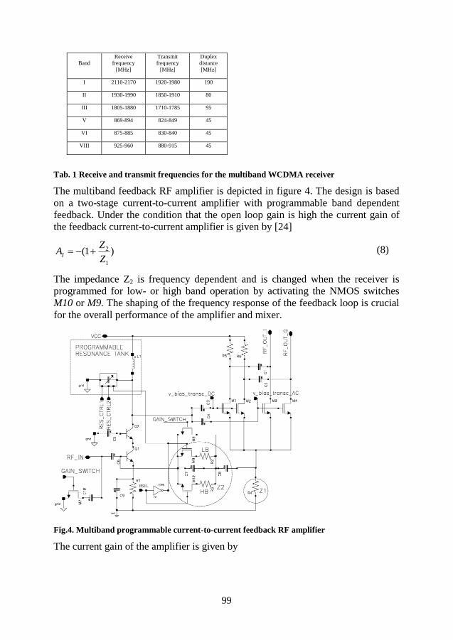
99
Band
Receive
frequency
[MHz]
Transmit
frequency
[MHz]
Duplex
distance
[MHz]
I 2110-2170 1920-1980 190
II 1930-1990 1850-1910 80
III 1805-1880 1710-1785 95
V 869-894 824-849 45
VI 875-885 830-840 45
VIII 925-960 880-915 45
Tab. 1 Receive and transmit frequencies for the multiband WCDMA receiver
The multiband feedback RF amplifier is depicted in figure 4. The design is based
on a two-stage current-to-current amplifier with programmable band dependent
feedback. Under the condition that the open loop gain is high the current gain of
the feedback current-to-current amplifier is given by [24]
)1(1
2
Z
ZAI (8)
The impedance Z2 is frequency dependent and is changed when the receiver is
programmed for low- or high band operation by activating the NMOS switches
M10 or M9. The shaping of the frequency response of the feedback loop is crucial
for the overall performance of the amplifier and mixer.
Fig.4. Multiband programmable current-to-current feedback RF amplifier
The current gain of the amplifier is given by

100
INRF
QOUTRFIOUTRF
II
IIA
_
____ (9)
The output signal from LNA (node RF_IN) is connected to the base of the bipolar
device Q1. The collector current of the input device equals 3.7mA. The emitter of
Q1 is connected through the resistor R1 to ground for bias stability purposes. Since
it is desired to have a low input impedance to the amplifier a capacitor is
connected across the resistor thereby creating a low impedance from the emitter of
Q1 for RF frequencies. The cascode is needed to increase the loop gain of the
amplifier. The loopgain of the feedback amplifier is defined as
1,
_
QB
INRF
I
ILG (10) (26)
The “error current” in the feedback system is equal to the base current, IB of input
transistor Q1.
With the LC-tank is possible to achieve a higher loop gain compared to what
would have been possible if the tank had been replaced with a purely resistive load
since there is no DC-drop. The third order linearity is thereby improved [25]. The
collector of Q2 is connected to the programmable resonance tank consisting of an
on-chip inductor, a fixed capacitor and three switched capacitors. The resonance
frequency of the tank is programmable to maximize the loop gain for the selected
band. Low or high band operation is controlled with the BSEL signal.
The output from the resonance tank is AC-coupled to the gates of the NMOS-
devices M1 and M2 and also AC-coupled to the NMOS devices M3 and M4. When
active these devices are biased with 3.13mA each. Depending on whether the
output to the mixer core should be DC- or AC-coupled, either devices M3 and M4
or M1 and M2 are turned on. For a certain TX power level a control signal should
be sent to the RF amplifier that disables the NMOS devices that are AC-coupled to
the output. The devices that are DC-coupled to the output are then enabled. This is
the current save mode of the architecture. The DC-current in the output NMOS is
reused as the mixer tail current. The feedback signal is connected from the source
terminals to the base of the input bipolar device through an AC-coupling An
interferer containing AM-modulation will generate a low frequency IM2-tone in
the transconductance NMOS. In the AC-coupled mode the IM2-tone is prevented
from reaching the mixer core by the AC-coupling of the output.
The mixer will downconvert noise from the amplifier not only at the LO-
frequency but also at odd harmonics of the LO-frequency. The Fourier series of
the square wave LO-signal contains only odd harmonics i.e. frequencies fLO, 3fLO,
5fLO… (2n+1)fLO. The contribution to the total noise figure from the higher
harmonics is significant, especially from the 3fLO frequency. To reduce the noise
figure of the amplifier and mixer it is important to reduce the mixer down
conversion of noise at higher harmonics. The resonance tank is tuned to the LO-
frequency. Far out from the LO-frequency, i.e. for higher harmonics the resonance
circuit will act as a shortcut to signal ground. The output noise will be heavily

101
attenuated. Closer to the resonance frequency, typically for the third harmonic of
the LO-frequency the amplifier still has a high open loop gain and the frequency
response is determined by the feedback net. The outlined feedback net with a band dependent pole in the impedance Z2 defined by the capacitor and either low
band (marked LB) or high band resistors (marked HB) solves this issue. The LC-
tank also improves the blocking performance of the feedback amplifier and mixer.
For frequencies close to the wanted signal for which the loopgain A is large the
two-stage amplifier will behave as a regular feedback current amplifier. For
frequencies far away from the resonance frequency the open loop gain of the
amplifier vanishes and any possible interferer will be short circuited to VCC.
The maximum power of the WCDMA wanted signal is–25dBm. In order not to
compress the mixer feedback loop with the wanted signal a gain switch is required
in the RF amplifier. The switch is implemented with an NMOS device across the
feedback net plus an NMOS in series with a capacitor connected to node RFIN.
The gain of the RF feedback amplifier is reduced to 0dB and the gain is further
reduced by shunting the RF input signal to ground
C. The LNA
The LNAs are standard bipolar cascode designs with inductive degeneration
matched to a 50Ω port. In band I and III the current consumption is 4.3mA while it
is 4.9mA in band VIII. The degeneration inductors are 650pH in band I, 850pH in
band III and 3nH in band VIII.
D. The single balanced mixer switching core
The switching mixer core consists of a main mixer (Q1 and Q2) that is DC-
coupled to the LO-driver and a trim mixer (Q3 and Q4) that is AC-coupled with
capacitors C1 and C2 to the LO-driver. Connected together as depicted in figure 5
these two mixers form a mismatch compensated mixer.

102
Fig.5. Switching mixer core
The two mixer cores share the same collector load. The load consists of the
resistors R1 and R2 together with the capacitors C5, C6, C7 and C8. Capacitors C5
and C6 filter common mode signals while C7 and C8 filter differential signals.
The WCDMA TX- signal that leaks into the receiver LNA through the finite
isolation of the duplexer will be downconverted to an IF-frequency by the RX LO-
signal. When transmitting at high power this TX-leakage signal is a strong
interferer that the receiver must be able to handle without compressing. The filter
at the mixer output will attenuate the IF-frequency so that the mixer feedback loop
does not compress even while transmitting at maximum power. The base bias
voltages of the trim mixer are determined by the output currents from the feedback
loop, connected at nodes I_trim_p and I_trim_n, in resistors R3 and R4. The
feedback loop will regulate these two currents so that the DC-offset at the mixer
output becomes 0V, i.e. VOut_BB_p = VOut_bb_n. The capacitors C3 and C4 attenuate
the LO voltage swing at the output of the feedback loop. Without these capacitors
unwanted modulation of the output current from the feedback circuit would occur.
The resistors R5 and R6 isolate the LO-signal from the signal ground generated by
capacitors C3 and C4. The input signal to the feedback loop is mixer output
voltages VOut_BB_p and VOut_bb_n. The RF signal from the current-to-current
feedback amplifier is connected in node IEE_main_RF. In order to have different
DC tail currents in the main- and trim mixer the RF signal must be AC-coupled
with capacitor C9 from node IEE_main_RF to node IEE_trim. For optimal operation
the ratio of the tail currents IDC_main and IDC_trim is typically around 10. In the
presented results the tail current in the main and trim mixer equals 3.3mA and
0.26mA respectively.
The mixer is not capable of suppressing any low frequency IM2-signals originating
from the current-to current amplifier. The RF input signal to the trim mixer is AC
coupled to the RF input of the main mixer. For the case of DC-coupling of the

103
output from the current-to-current amplifier a low frequency IM2-signal from this
stage reaches the main mixer but not the trim mixer. If mismatch is present in the
main mixer the mixer feedback loop will compensate this by offsetting the trim
mixer but the feed through of the IM2-component through the main mixer will still
be the same.
For high IM2 suppression it is important that all component mismatches besides
mismatch in the mixer core switching devices is minimized by up scaling of the
device sizes as well as careful layout. If the mixer load resistors R1 and R2 are
mismatched the feedback loop will also try to compensate the DC-offset generated
by this mismatch. However, the loop will then create a DC-offset between the
bases in the trim mixer. This will then generate a poor IM2 performance in the
compensated mixer core due to Vbe mismatch but there will still also be an IM2-
component originating from the load resistor mismatch. It is not possible to reduce
the total IM2-distortion by compensating resistor load mismatch with Vbe
mismatch in the mixer core. Due to switching speed requirements scaling up the
active devices in the mixer core is only possible to some amount. The two devices
in the trim mixer core, Q3 and Q4, can also be mismatched. In the case of
mismatch in this part the feedback loop will also compensate the DC-voltage at the
mixer output originating from this mismatch.
E. The mixer feedback loop
The feedback loop is acting on the DC-offset at the mixer output. There are two
identical filters, one for the I-channel mixer and one for the Q-channel mixer. The
filter is a two-stage design with the first stage acting as a low pass filter and the
second stage operating as a transconductance that generates the feedback current
to the trim mixer. Figure 6 outlines the filter architecture. The outputs from the
mixer are connected to Q1 and Q2. The low pass filter has both common-mode
filtering with capacitors C0 and C2 and differential mode filtering by capacitor C1.
The cut-off frequency is set by the external differential capacitor C1. In order to
minimize the required size of C1 the resistive load is large.

104
Fig.6. Mixer feedback loop
To handle the DC voltage drop across the load without forward biasing the base-
collector junction of Q1 and Q2, the tail current of the stage is low (20A). The
stage is degenerated with resistors R1 and R2 to increase the compression point.
The degeneration resistors R4 and R5 in the second stage have two purposes. They
increase the input impedance to the second stage as well as they increase the
compression point. If the input impedance to the second stage is too low the filter
cut-off frequency is set by this impedance instead of the high resistive load of the
first stage. The second stage tail current equals 300A. The feedback loop is
dimensioned to be able to handle a certain level of mismatch in the main mixer
core without running into compression. Both the low pass filter stage and the
transconductance stage are heavily degenerated with resistors in order to increase
the compression point. The feedback loop is only active for low frequencies i.e.
DC plus a few kilohertz. The performance of the feedback mixer is sensitive to
mismatch in the loop devices since this will create a mixer DC-offset that the
feedback loop will counteract by offsetting the trim mixer. Since the bandwidth of
the feedback loop should be as low as possible there is no penalty for increased
capacitance due to upscaling of the devices in the loop to improve the matching.
The loop is disabled by shorting the second stage input to a bias voltage. The pole
frequency defined by capacitor C1 and resistors R9 and R10 must be designed low
enough that resistor process spread does not increase the cut-off frequency above a
value that can be tolerated. The biasing of the loop should be designed for
temperature stability of the of the loop output currents I_trim_n, I_trim_p,
IEE_main and IEE_trim. Supply voltage variations do not impact the loop
performance.

105
F. The resulting LO-leakage
LO-leakage at node IEE_main_RF together with an AM-modulated interferer, i.e. a
WCDMA TX-signal will generate a second order signal in the mixer due to cross
modulation. The downconverted AM-modulated LO-leakage generates a baseband
frequency at the AM-modulation frequency.
If the device mismatch in the main mixer (or in the trim mixer) increases, the LO-
leakage in node IEE_main_RF will also increase if not compensated by the mixer
feedback loop. The capability of the loop to reduce the LO-leakage as well as the
IM2 product can be evaluated by inserting a voltage source as Vbe mismatch
between the emitter of the mixer core device Q1 and node IEE_main_RF. The
mismatch will cause a DC-current imbalance as well as a LO-leakage imbalance
between Q1 and Q2. The differential LO-signals LO_p and LO_n no longer cancel
each other in node IEE_main_RF. The DC-current mismatch will create a DC-
voltage offset at the mixer output that the feedback loop will counteract by
changing the feedback currents I_trim_n and I_trim_p and offsetting the trim
mixer. If the LO-leakage signal from the trim mixer is added to the LO-leakage
from the main mixer in node IEE_main_RF the level of the summed LO-leakage is
strongly attenuated. The benefit of the feedback is illustrated in figure 7
illustrating the difference in LO-leakage level in node IEE_main_RF o f the I-mixer
versus Vbe mismatch (x-axis variable emi_missm) between the mixer with
feedback and with the feedback disabled.
When for a comparing simulation the feedback loop was disabled, the load of the
first stage in the feedback path was shorted. The simulation was made with the
SpectreRF PSS tool. The LO-frequency was 2200MHz and the interferer
frequency was 2000MHz, i.e. the fundamental frequency fPSS-fund was 200MHz.
Fig.7. LO-leakage in dBVp in node I_tail_main_RF_in versus Vbe mismatch with and without
feedback

106
The 11: th harmonic of the fundamental frequency equals the LO frequency. The
attenuation of the LO-leakage is 10dB with the mixer loop turned on. With the
loop off the fLO-leakage current at node IEE_main_RF is 5Arms for 4mV Vbe
mismatch. The loop will attenuate the leakage at frequencies (2n+1)fLO as well.
G. IM2 distortion from cross modulation
The AM-modulation of the TX-interferer will be transferred on to the LO-leakage
at the input of the main- as well as the trim mixer through cross modulation. In
linear scale the IM2 cross modulation component is proportional to 2
3_ / IPV leakLO
where VLO_leak is the LO-leakage level at the mixer input. In case of mismatch in
the main mixer, like less DC-current in the left main mixer device, the phase of the
LO-leakage will be degrees at the input of the main mixer. Since the trim mixer
will counteract the DC-offset generated by the main mixer the right device of the
trim mixer will have a higher DC-current. The LO-leakage at the input of the trim
mixer will therefore be at the phase +180 degrees. The generated IM2cross
collector currents from the main- and trim mixer will therefore counteract each
other. The IM2 level and DC-offset at the I-mixer differential output versus main
mixer Vbe mismatch (x-axis variable emi_missm) with and without feedback are
shown in figure 8 and 9 respectively. The simulation setup is identical to the setup
for figure 7. The AM-modulated TX-interferer is represented by one interferer at
2000MHz (PSS-frequency) and another at 2000 MHz + 30 kHz (pac-frequency).
Harmonic –10 equals the IM2 product according to
fundPSSpacIM fkff 2 (11)
The input power of both signals was –33dBm at the LNA input. The suppression
of IM2 product as well as DC offset is working as intended. The IM2 level
improvement is varying with the main mixer Vbe mismatch. Smaller variations are
due to simulator accuracy. The improvement is reduced for very high offset
voltages. Since the tail current in the trim mixer is 10 times smaller compared to
the main mixer tail current a larger relative change in the trim mixer collector
currents is required to compensate for a mismatch in the trim mixer. This will
cause the IIP3 of the trim mixer devices to be different and an IM2cross current is
generated that is not optimal for cancellation. The trim mixer tail current and
device sizes can be modified for tuning of the IM2-suppression.

107
Fig.8. Differential IM2 level in dBVp at mixer I output versus Vbe mismatch with and without
feedback
Fig.9. Differential DC-offset in mV at mixer I output versus Vbe mismatch with and without
feedback
H. High pass characteristic of the mixer baseband output signal
With the feedback loop on the mixer output will have a high pass characteristic,
i.e. the conversion gain for RF-frequencies very close to the LO-signal is reduced
compared to the gain for RF-frequencies further away from the LO-signal. This is
undesired since a WCDMA signal includes low frequency modulation. The reason
for this is that the cut-off frequency for the low pass filter in the feedback loop is
not infinitely low. Due to the finite rise- and fall time of the trim mixer there is a
certain feed through of low frequency signals from the base to the collector of the
mixer trim devices. The collector signal current originating from low-frequency
feed through will add in opposite phase to the baseband current created from down
conversion of the RF-signal in the main- and trim mixer. A smaller tail current in
the trim mixer results in less feed through. For a given pole location in the mixer
feedback loop the high pass cut-off frequency is lowered for a smaller tail current
of the trim mixer. A solution based on only the trim mixer and no main mixer
would require a significantly larger low pass filter capacitor. The required filter
capacitor is intended to be placed off-chip, preferably on a laminate inside the
package not to increase the pin-count. The required pole location for maintained
bit error rate, BER, depends on the modulation scheme of the received signal.

108
WCDMA modulation with QPSK-modulation can tolerate a pole at
7 kHz while WCDMA with 16-QAM modulation, i.e. HSDPA, requires a pole
location lower than 1 kHz. The loop gain of the feedback mixer will vary with the
baseband frequency. The loop gain at baseband frequency f will be the difference
between the maximum conversion gain and the conversion gain at frequency f
(f<fmax). For frequencies higher than the cut-off frequency of the low pass filter the
loop gain approaches 0dB.
I. Trim mixer and RF feedback amplifier AC-coupling shut down modes
When the mobile is transmitting at a low power <<+24dBm the requirement on the
mixer IP2 is very much relaxed. The baseband frequency response of the mixer can
be made flat from DC to the cut-off frequency defined by the mixer pole by
shutting down the trim mixer. Shutdown is implemented by turning off the bias to
the first stage in the feedback loop. The input to the second stage is instead biased
with switches connected to a voltage source as illustrated in figure 6. Since there is
no need for low second order distortion the AC-coupling of the feedback RF
amplifier transconductance stage should be turned off as well to save current. With
the mixer loop on and DC-coupled RF amplifier to save current the mixer DC
offset is maintained low.
J. Suppression of noise from the feedback loop with the trim mixer
The trim mixer has its base terminal AC-coupled to the base terminal of the main
mixer. The emitter of the trim mixer is also AC-coupled to the emitter of the main
mixer. The output signal from the mixer feedback is connected to the base of the
trim mixer. The architecture has the big advantage that no low frequency noise
from the feedback loop can reach the bases of the main mixer. The trim mixer
though has a certain feed through of low frequency noise from the feedback loop
but since the tail current of the trim mixer is only a fraction of the tail current in
the main mixer the contribution from the feedback loop noise to the overall noise
figure is very much reduced.
K. The LO-driver
The LO-signal to the mixer is provided through a standard IQ-divider circuit
generating clock signal with 50% duty cycle. It is important to provide the mixer
with a LO-signal with short rise- and fall time otherwise the IM2-performance will
degrade.

109
V. SIMULATED PERFORMANCE
A. Specifications and calculations
The design was made for a system specified to have 32dB voltage gain from the
50 LNA input to the differential output of the mixer. The half-duplex IIP3 of the
LNA and mixer should be at least –9dBm. The IIIP2 for a two-tone TX-interferer
should be at least +47dBm. The maximum TX-output level at the antenna is
+24dBm. The corresponding output power from the PA is +26dBm assuming 2dB
loss. The duplexer was assumed to have 52dB isolation from TX to RX resulting
in +26-52= -26dBm TX power at the LNA input. For the simulations an input
power of PT = -33dBm was selected because the compression point of the mixer is
at least -23dBm. When simulating the IM2 product with SpectreRF PSS and PAC
the small signal pac signal must be at least 10dB below the compression point for
the results to have good accuracy. If the input signal PT = -33dBm and IIP2 equals
+47dBm then the IM2 level at the input of the LNA is at -113dBm using (2). In a
50-system this corresponds to -126dBVrms. (27)
At the mixer output the following applies with the conversion voltage gain equal
to Gv.
vffIMiffIMoutmix GPV 13)_(2_)_(2__ 2121 (12)
Using (12), the IM2-level at the differential mixer output is at
-113 -13 +32 = -94dBVrms = -91dBVp. The cross modulation product is calculated
using (7). Calculated back to the LNA input 5Arms fLO-leakage current for 4mV
mismatch at node IEE_main_RF with the feedback loop off corresponds to
34Vrms, i.e. –76dBm. The average TX-leakage power equals the sum of the TX
interferer sideband powers of -33dBm, i.e.–30dBm. Using IIP3= -9dBm, (7) gives
Pi_crossmod = -112dBm from cross modulation of the fundamental LO-leakage tone.
Taking account for cross modulation of odd harmonics to fLO the total cross
modulation power is even higher. Using (2) with only a second order nonlinearity
accounted for, Pi_IM2 equals –113dBm for a receiver with IIP2= +47dBm and two
TX interferer sidebands at –33dBm. The maximum LNA input power of the half-
duplex interferer is –46dBm. The largest IM3 product is created when the TX-
leakage is at its maximum i.e. –26dBm. Using (1) the IM3 product at the
differential mixer output then equals –78dBVp for IIP3 = -9dBm.
B. Simulated performance of the LNA and feedback amplifier standalone
For evaluation of the LNA and RF feedback amplifier standalone the mixer load of
the NMOS output transistors was replaced with 10-ohm resistors. The inductance
was represented with an s-parameter model of a real on-chip inductor. The lumped
model has L=8.4nH and Rs=16. Looking from the cascode device Q9, Q=8.5 in
band I and 5.4 in band VIII. The current gain is defined as the sum of the NMOS
drain current to the I- and Q-mixer divided by the amplifier input current. The
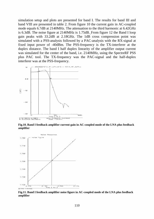
110
simulation setup and plots are presented for band I. The results for band III and
band VIII are presented in table 2. From figure 10 the current gain in AC-coupled
mode equals 6.7dB at 2140MHz. The attenuation to the third harmonic at 6.42GHz
is 6.3dB. The noise figure at 2140MHz is 1.75dB. From figure 12 the Band I loop
gain peaks with 33.2dB at 2.18GHz. The 1dB cross compression point was
simulated with a PSS-analysis followed by a PAC-analysis with the RX-signal at
fixed input power of -40dBm. The PSS-frequency is the TX-interferer at the
duplex distance. The band I half duplex linearity of the amplifier output current
was simulated for the center of the band, i.e. 2140MHz, using the SpectreRF PSS
plus PAC tool. The TX-frequency was the PAC-signal and the half-duplex
interferer was at the PSS-frequency.
Fig.10. Band I feedback amplifier current gain in AC-coupled mode of the LNA plus feedback
amplifier
Fig.11. Band I feedback amplifier noise figure in AC-coupled mode of the LNA plus feedback
amplifier

111
Fig.12. Band I loopgain of the RF feedback amplifier
The IM3-level at the amplifier current output was back calculated to the LNA input
using the transconductance of the LNA and feedback amplifier. The IIP3 was
calculated using the relation (1). The in-band IIP3 was simulated with a PSS-
frequency at 2140MHz and a PAC signal at 2141MHz. The performance of the RF
feedback amplifier in band I, III and VIII is summarized in table 2.
Parameter Band I Band III Band VIII
Current consumption [mA] 10 10 10
Transconductance of LNA and feedback amp.(I+Q) [mS] 280 306 284
Feedback amplifier current gain at band center [dB] 6.7 7.0 6.5
Attenuation of 3*fLO in DC/AC-coupled mode 6.9/6.3 8.0/7.5 11.6/11.2
NF [dB] 1.75 1.69 1.98
Loopgain [dB] 34.3 32.8 29.5
Cross compression point for a TX interferer [dBm] -22.1 -21.9 -23.1
Small signal in-band IIP3 [dBm] -6.9 -7.5 -8.5
Small signal half-duplex IIP3 including ideal LNA [dBm] -5.6 -6.0 -7.6
Large signal half-duplex IIP3 including ideal LNA [dBm] -5.8 -6.0 -7.8
Tab.2. Performance summary of the RF feedback amplifier
C. Simulated results for the RF feedback amplifier together with the
feedback mixer
To shorten the time for the simulator to reach convergence, the pole in the mixer
feedback is set higher than it should be in a real design. The size of the external
capacitor is 6nF. All figures are simulation results for band I. The gain and noise
figure depicted in figure 11 and 12 was simulated with a PSS-analysis plus PXF
and PNOISE analysis. For the pnoise analysis 20 sidebands were accounted for. In

112
AC-coupled mode with the LO frequency at 2140MHz, NFDSB = 2.6dB at 1MHz.
The loop gain at a baseband frequency below the cut off frequency is the
difference between the in band maximum gain and the gain at the baseband
frequency. At DC the conversion gain is 12.4dB resulting in a loop gain of
19.5dB. The gain of the first stage in the feedback loop equals 10dB giving a gain
of 9.5dB in the second stage of the loop. The mixer feedback loop stability is
guaranteed by the both the low pass filter in the mixer feedback loop and the low
pass filter at the mixer output. The feedback factor is negligible for frequencies
above the mixer feedback loop cut-off frequency. For low frequencies where there
is a significant loop gain the phase change of the feedback signal relative to DC is
very small. For frequencies above the mixer output cut-off frequency the input
signal to the loop is heavily attenuated.
Fig.11. Band I gain in AC-coupled mode

113
Fig.12. Band I noise figure in AC-coupled mode
The conversion gain equaled 31.9dB at 100 kHz with high pass BW3dB = 4.0 kHz
and low pass BW3dB = 6.5MHz. In the noise summary the largest contributions
comes from the divider, the RF amplifier output stage and the main mixer tail
current device. The NFDSB increases below the cut-off frequency. This is due to
feed through of unfiltered noise from the feedback loop through the trim mixer. In
DC-coupled mode the noise figure at 1MHz is improved due to that the main
mixer current generator is off. The mixer feedback loop does not affect the mixer
noise figure for frequencies above the cut-off frequency of the low pass filter. For
lower frequencies the main excess noise originates from the active devices and
degeneration resistors in the first stage of the low pass filter together with the base
current of the main mixer transistors.
The second order distortion was simulated with a Monte Carlo analysis [26], [27]
using a PSS +PAC analysis. With the Monte Carlo tool a random mismatch is
applied to all devices in the design for each simulation run. The standard deviation
of the mismatch distribution for each device type is determined by process data.
100 iterations were made with the mixer feedback loop both on and off to verify
the effect of the loop. To be able to use the PSS-tool the duplex distance was set to
200MHz instead of 190MHz. With the PSS frequencies fLO = 2200MHz,
fTX1=2000MHz and the PAC frequency fTX2 = 2000.03MHz the IM2 product is at
30 kHz. The input powers of fTX1 and fTX2 were at –33dBm each. With 32dB
conversion gain the IM2 limit at the mixer output then is at
-91dBVp. With the mixer feedback loop turned on the average IM2 level in the I-

114
and Q-channel is -102dBVp and -100dVp which corresponds to I-channel
IIP2 = +59dBm and Q-channel IIP2 =+56dBm. The average DC-offset is 104V in
the I-mixer and 110V in the Q-mixer. Histogram of the I-mixer IM2-levels in
dBVp and DC-offset at the mixer outputs with the loop on are depicted in figure
13.
Fig.13. Band I histogram of I-mixer IM2 in dBVp and DC-offset at the differential mixer output
versus iteration number with the mixer feedback loop on
With the feedback loop turned off as depicted in figure 14 for the I-mixer more
than 19 iterations fall outside -92dBVp. The average DC-offset increases a factor
8. The worst sample with the loop off is at -84dBVp corresponding to IIP2 =
+40dBm. Comparing the histograms, the turned-on loop results in a distribution
peak around –100dBVp while the turned-off loop results in more evenly
distributed values with a large number of iterations close to the specification limit.
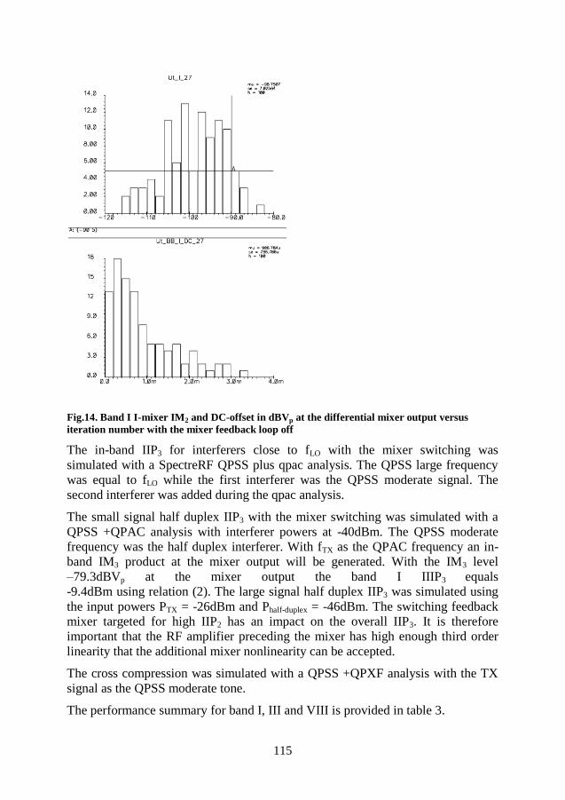
115
Fig.14. Band I I-mixer IM2 and DC-offset in dBVp at the differential mixer output versus
iteration number with the mixer feedback loop off
The in-band IIP3 for interferers close to fLO with the mixer switching was
simulated with a SpectreRF QPSS plus qpac analysis. The QPSS large frequency
was equal to fLO while the first interferer was the QPSS moderate signal. The
second interferer was added during the qpac analysis.
The small signal half duplex IIP3 with the mixer switching was simulated with a
QPSS +QPAC analysis with interferer powers at -40dBm. The QPSS moderate
frequency was the half duplex interferer. With fTX as the QPAC frequency an in-
band IM3 product at the mixer output will be generated. With the IM3 level
–79.3dBVp at the mixer output the band I IIIP3 equals
-9.4dBm using relation (2). The large signal half duplex IIP3 was simulated using
the input powers PTX = -26dBm and Phalf-duplex = -46dBm. The switching feedback
mixer targeted for high IIP2 has an impact on the overall IIP3. It is therefore
important that the RF amplifier preceding the mixer has high enough third order
linearity that the additional mixer nonlinearity can be accepted.
The cross compression was simulated with a QPSS +QPXF analysis with the TX
signal as the QPSS moderate tone.
The performance summary for band I, III and VIII is provided in table 3.

116
Parameter Band I Band III Band VIII
Supply voltage [V] 2.7 2.7 2.7
Current consumption in DC/AC-coupled mode
[mA] 15.0/21.7 15.0/21.7 15.5/22.3
Voltage gain in DC/AC-coupled mode [dB] 32.0/31.9 32.4/32.3 32.1/32.0
NFDSB@1MHz in DC/AC-coupled mode [dB] 2.32/2.60 2.20/ 2.45 2.53/ 2.77
Avg/min IIP2 in AC-coupled mode from 100
MC iterations [dBm] +58/+47 +59/+45 +57/+47
Avg/max DC-offset in I-and Q mixer AC-
coupled mode from 100 MC iterations [V] 107/430 91/380 86/370
In-band IIP3 [dBm] -10.7 -10.9 -10.0
Small/large signal half-duplex IIP3 [dBm] -9.4/-9.4 -9.2/-9.3 -9.3/-9.3
Cross compression with a TX interferer [dBm] >-23.0 >-23.0 >-23.5
Tab.3. Performance summary for feedback mixer and amplifier
VI. CONCLUSIONS
The benefit of the presented architecture is that it provides a multiband single
ended LNA and single ended mixer with high enough second- and third order
linearity that it is functional in a WCDMA system without a SAW-filter. The DC-
offset at the mixer output is strongly attenuated which is beneficial for the
following stages, i.e. baseband filter and ADC. The attenuation of the DC-offset
and the increase of the IP2 were achieved by the described method to reduce the
effect of the switching mixer core device mismatch using a feedback loop. The
third order nonlinearity performance as well as the low noise figure was possible
to achieve through the programmable RF feedback current-to-current amplifier
preceding the mixer. The LNA is single ended which is especially beneficial for a
multiband solution since only one package pin is required for each band. Since the
programmable feedback RF amplifier is multiband only one low-Q on-chip
inductor is needed. The required filter capacitor is preferably placed inside the
package. The architecture was designed in a BiCMOS process but the described
advantages could be applied to a CMOS only design as well.
ACKNOWLEDGEMENT
The author would like to thank Prof. Pietro Andreani at Department of Electrical
and Information Technology, Lund University for his valuable input concerning
the editing of this paper.
REFERENCES
[1] L. Sheng, L. E. Larsson, “An Si–SiGe BiCMOS Direct-Conversion Mixer with
Second-Order and Third-Order Nonlinearity Cancellation for WCDMA

117
Applications”, IEEE Transactions on Microwave Theory and Techniques, vol. 51,
no. 11, pp. 2211-2220, Nov 2003
[2] N. Swanberg, J. Phelps, M. Recouly, “WCDMA cross modulation effects and
implications for receiver linearity requirements”, in the proceedings of Radio and
Wireless Conference, 2002. RAWCON 2002. IEEE, ISBN: 0-7803-7458-4, pp. 13-
18, 2002
[3] Q. Huang, J. Rogin, X. Chen, D. Tschopp, T. Burger, T. Christen, D.
Papadopoulos, I. Kouchev, C. Martelli, T. Dellsperger,” A Tri-Band SAW-less
WCDMA/HSPA RF CMOS Transceiver with On-Chip DC-DC Converter
Connectable to Battery”, in the proceedings of 2010 IEEE International Solid-
State Circuits Conference ( ISSCC), ISBN 0193-6530, pp. 60-61, San Francisco,
2010
[4] Chris W. Liu, Morten Damgaard, Broadcom Corporation, “IP2 and IP3
Nonlinearity Specifications for 3G/WCDMA Receivers, Microwave journal, May
2009
[5] Walid Y. Ali-Ahmad, “Effective IM2 estimation for two-tone and WCDMA
modulated blockers in zero-IF, Rfdesign, April 2004
[6] B. Razavi, “Design Considerations for Direct-Conversion Receivers,” IEEE
Transactions on Circuits and Systems—II: Analog and Digital Signal Processing,
vol.44, no. 6, pp. 428-435, June 1997
[7] B. Gilbert, “Design considerations for active BJT mixers,” in Low-Power HF
Microelectronics; A Unified Approach, G. Machado (Ed.), London, IEE, Ch. 23,
1996.
[8] D. Coffing, E. Main, “Effects of offsets on bipolar integrated circuit even-order
distortion terms,” IEEE Transactions on Microwave Theory Tech., vol. 49, no. 1,
pp. 23-30, Jan. 2001
[9] Elahi, I. Muhammad, K. Balsara, P.T. ”IIP2 and DC Offsets in the Presence of
Leakage at LO frequency”, IEEE Transactions on Circuits and Systems II:
Express Briefs”, vol. 53, no. 8, pp. 647-651 Aug 2006
[10] Elahi, I. Muhammad, K.R. ”Asymmetric DC offsets and IIP2 in the Presence
of LO Leakage in a Wireless Receiver”, in the proceedings of 2007 IEEE Radio
Frequency Integrated Circuits (RFASIC) Symposium, ISBN 1-4244-0530-0, pp.
313-316, 2007
[11] Elahi, I. Muhammad, K.R. ”IIP2 Calibration by Injecting DC offset at the
Mixer in a Wireless Receiver”, IEEE Transactions on Circuits and Systems II:
Express Briefs”, vol. 54, no. 12, pp. 1135-1139, Aug 2007
[12] Belveze F, Baudin, P. “Specifying receiver IP2 and IP3 based on tolerance to
modulated blockers”, IEEE Transactions on Communications, vol 56, no. 10, pp.
1677-1682, Oct 2008

118
[13] Qizheng Gu, “RF system design of transceivers for wireless communication”,
Springer, ISBN 0-387-24161-2, 2005
[14] K. Kivekas, A. Parssinen, J. Ryynanen, J. Jussila, K. Halonen, ”Calibration
Techniques of Active BiCMOS Mixers”, IEEE Journal of Solid-State Circuits,
vol. 37, pp. 766-769, June 2002.
[15] M. Hotti, J. Ryynanen, K. Kivekas, K. Halonen,”AN IIP2 CALIBRATION
TECHNIQUE FOR DIRECT CONVERSION RECEIVERS”, in the proceedings
of 2004 International Symposium on Circuits and Systems, ISCAS 2004, ISBN 0-
7803-8251-X, vol. 4, pp 257-260, 2004
[16] K. Kivekas, A. Parssinen, K. Halonen,”Characterization of IIP2 and DC-
Offsets in Transconductance Mixers”, IEEE transactions on Circuits and Systems-
II: Analog and Digital Signal Processing, vol. 48, no. 11, pp. 1028-1038, Nov
2002.
[17] Mikko Hotti, Jussi Ryynänen, Kari Halonen, “RC-load Analysis of the
Downconversion Mixer IIP2” in the proceedings of 2005 European Conference on
Circuit Theory and Design, ISBN 0-7803-9066-0, vol. 1, pp. I/237-I/240, 2005
[18] Massimo Brandolini, Paolo Rossi, Davide Sanzogni, Francesco Svelto, “A
+78dBm IIP2 CMOS Direct Downconversion Mixer for Fully Integrated UMTS
Receivers”, IEEE Journal of Solid-State Circuits, vol. 41, no. 3, pp. 552-559,
March 2006.
[19] Massimo Brandolini, Marco Sosio, Francesco Svelto, “A 750mV Fully
Integrated Direct Conversion Receiver Front-End for GSM in 90-nm CMOS”,
IEEE Journal of Solid-State Circuits, vol. 42, no. 6, pp. 1310-1317, June 2007
[20] P. Sivonen, Ari Vilander, Aarno Pärssinen, ”Cancellation of Second-Order
Intermodulation Distortion and Enhancement of IIP2 in Common-Source and
Common-Emitter RF Transconductors” IEEE Transactions on Circuits and
Systems”, vol. 52 no. 2, pp. 305-317, Feb 2005
[21] S. Rodriguez, A.Rusu, L-R.Zheng, M.Ismail, “CMOS RF mixer with digitally
enhanced IIP2”, Electronics Letters, vol. 44, no. 2, pp. 121-122, Jan. 2008
[22] K. Dufrene, Z. Boos, R. Weigel, “Digital Adaptive IIP2 Calibration Scheme
for CMOS Downconversion Mixers”, IEEE Journal of Solid-State Circuits, vol.
43, no. 11, pp. 2434-2445, Nov 2008
[23] Y. Feng, G. Takemura, S. Kawaguchi, N. Itoh, P. Kinget, “A Low Power
Low Noise Direct Conversion Front-End with Digitally Assisted IIP2 Background
Self Calibration”, in the proceedings of 2010 IEEE International Solid-State
Circuits Conference (ISSCC), ISBN 978-1-4244-6033-5, pp. 70-71, 2010
[24] E. M Cherry, D. E. Hooper, “Amplifying Devices and Low-Pass Amplifying
design”, Wiley, ISBN 978-0471153450, 1968

119
[25] A. A. Abidi, “General relations between IP2, IP3, and offsets in differential
circuits and the effects of feedback,” IEEE Transactions on Microwave Theory
Tech., vol. 51, no. 5, pp. 1610-1612, May 2003.
[26] Vahidfar, M.B. Shoaei, O. “A High IP2 Mixer Enhancement by a New
Calibration Technique for Zero-IF Receivers”, IEEE Transactions on Circuits and
Systems II: Express Briefs, vol. 55, no. 3, pp. 219-223, March 2008
[27] M. Voltti, T. Koivisto, E. Tiiliharju, ”Statistical performance of IIP2 in active
and passive mixers”, in the proceedings of Research in Microelectronics and
Electronics, 2008. PRIME 2008. Ph.D, pp. 161-164, ISBN 978-1-4244-1983-8,
Istanbul, 2008

120
Paper II

121
Paper II
Single-Ended Low Noise Multiband
LNA with Programmable Integrated
Matching and High Isolation Switches
Abstract
This paper describes a novel 90nm single-ended multiband input LNA preceded
by RF input switches connected to an on-chip balun intended to drive a differential
mixer. The architecture achieves a low noise figure of 1.8dB. The advantage with
the proposed architecture is that it is fully single-ended with on-chip
programmable narrow-band matching eliminating the need of off-chip
components. Especially in multiband integrated radios a single-ended LNA is
highly desirable since the pin-count for the LNAs is reduced by half compared
with a differential architecture. The PCB routing of the RF input signal is
simplified. Narrow-band matching is advantageous compared to common
broadband matching since this adds attenuation of out of band interferers and
suppresses conversion of 3rd
LO harmonic. This is important for the coexistence of
cellular systems with e.g. WLAN 802.11a operating in the 5GHz band.

122
I. INTRODUCTION
In a common multiband receiver as depicted in figure 1 there is one separate LNA
for each frequency band plus one duplexer connected to each RF input required to
attenuate the TX signal that leaks into the LNA. The duplexer typically provides
some 50-55dB isolation from TX to RX. The TX leakage into the active LNA is
also affected by the leakage through the non-active duplexers and LNAs. The
receiver is degraded by the TX-leakage through intermodulation generated by
second- and third order distortion.
Fig.1. TX-leakage paths in a common multiband LNA
The presented architecture depicted in figure 2 is based on only one single ended
LNA with programmable on-chip input matching preceded by on-chip RF input
switches. A tunable on-chip balun between the LNA and mixer creates a
differential RF signal for the mixer. The differential mixer is advantageous
regarding second order distortion. The presented input RF switches provide a
combination of low on-resistance together with high isolation for TX-leakage
while turned off. The multiband LNA is designed for WCDMA band I, II and III
plus DCS and PCS EGSM.
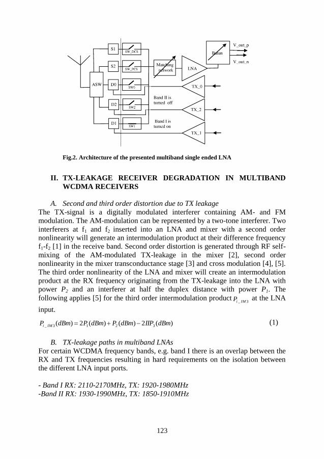
123
Fig.2. Architecture of the presented multiband single ended LNA
II. TX-LEAKAGE RECEIVER DEGRADATION IN MULTIBAND
WCDMA RECEIVERS
A. Second and third order distortion due to TX leakage
The TX-signal is a digitally modulated interferer containing AM- and FM
modulation. The AM-modulation can be represented by a two-tone interferer. Two
interferers at f1 and f2 inserted into an LNA and mixer with a second order
nonlinearity will generate an intermodulation product at their difference frequency
f1-f2 [1] in the receive band. Second order distortion is generated through RF self-
mixing of the AM-modulated TX-leakage in the mixer [2], second order
nonlinearity in the mixer transconductance stage [3] and cross modulation [4], [5].
The third order nonlinearity of the LNA and mixer will create an intermodulation
product at the RX frequency originating from the TX-leakage into the LNA with
power P2 and an interferer at half the duplex distance with power P1. The
following applies [5] for the third order intermodulation product3_ IMiP at the LNA
input.
)(2)()(2)( 3213_ dBmIIPdBmPdBmPdBmP IMi (1)
B. TX-leakage paths in multiband LNAs
For certain WCDMA frequency bands, e.g. band I there is an overlap between the
RX and TX frequencies resulting in hard requirements on the isolation between
the different LNA input ports.
- Band I RX: 2110-2170MHz, TX: 1920-1980MHz
-Band II RX: 1930-1990MHz, TX: 1850-1910MHz

124
When the receiver in figure 1 is configured for band I, LNA 1 is active and LNA 2
is turned off. At maximum output power the duplexer 1 input power is +26dBm.
There is 0dB attenuation in the duplexer 1 from the TX input to the antenna
switch (ASW) input. The isolation in the antenna switch between duplexer1 and 2
is rather poor, i.e. 20dB. Since the band 1 TX frequency overlaps the band II RX
frequency there is no attenuation in duplexer 2 for this TX interferer. The TX
power at the turned off band II LNA input is therefore equal to +6dBm. Assuming
52dB isolation in the duplexer, the TX power at the band 1 LNA originating from
the duplexer isolation then equals -26dBm. A second TX leakage originates from
the finite isolation between the LNA2 and LNA1 inputs. In order for this leakage
to be 10dB less than the duplexer leakage the LNA input isolation must exceed
42dB.
Narrow band input matching together with a balun is advantageous for the issue of
coexistence of cellular systems and WLAN. The upper part of the WLAN 802.11a
band is at 5.8GHz [6]. The isolation [7] between the WLAN and cellular antenna
is rather low, i.e. 15dB. The cellular duplexer does not attenuate the 5.8GHz
interferer more than 50dB. At maximum WLAN output power, i.e. +20dBm the
cellular receiver sees an interferer of -45dBm @5.8GHz. If a wideband LNA is
used and the RX mixer is driven by a square wave LO the only selectivity
available is the -9.5dB from the third harmonic down conversion [8]. Down
converted the WLAN interferer corresponds to a -54.5dBm in band interferer in
band II and PCS @1933MHz. Narrow band input matching together with a balun
as in the presented multiband LNA is capable of adding additional selectivity to
attenuate the 5.8GHz interferer.
III. DETAILED DESCRIPTION OF THE ARCHITECTURE
A. Packaging technology and grounding
The design is intended to be used with a WLP package [9] which is a package type
with the die flipped upside down. With this package the smallest inductance from
a die ground pad to the PCB ground is approximately 200pH. Each RF input
switch depicted in figures 2 and 4 is associated with a dedicated ground
connection gnd_switch_n where n=1...5. The LNA has a dedicated separate
ground gnd_chip as illustrated in figure 3. The gnd_chip ground is connected to
the PCB ground through four parallel inductance traces.
B. Input impedance of the inductively degenerated LNA
The inductively source degenerated MOS LNA has the advantage that it creates a
real part of the input impedance without adding a resistor [10].
)1
(gs
ss
gs
min
CLjL
C
gZ
(2)
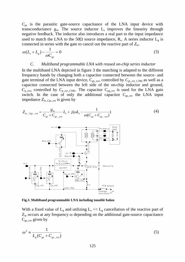
125
Cgs is the parasitic gate-source capacitance of the LNA input device with
transconductance gm. The source inductor Ls improves the linearity through
negative feedback. The inductor also introduces a real part to the input impedance
used to match the LNA to the 50 source impedance, Rs. A series inductor Lg is
connected in series with the gate to cancel out the reactive part of Zin.
01
)( gs
gsC
LL
(3)
C. Multiband programmable LNA with reused on-chip series inductor
In the multiband LNA depicted in figure 3 the matching is adapted to the different
frequency bands by changing both a capacitor connected between the source- and
gate terminal of the LNA input device, Cgs_ext, controlled by Cgs_ext_CTRL as well as a
capacitor connected between the left side of the on-chip inductor and ground,
Cp_ext, controlled by Cp_ext_CTRL. The capacitor Cpg_ext is used for the LNA gain
switch. In the case of only the additional capacitor Cgs_ext the LNA input
impedance Zin_Cgs_ext is given by
))(
1(
__
__
extgsgs
ss
extgsgs
mextCgsin
CCLjL
CC
gZ
(4)
Fig.3. Multiband programmable LNA including tunable balun
With a fixed value of Lg and utilizing Ls << Lg cancellation of the reactive part of
Zin occurs at any frequency depending on the additional gate-source capacitance
Cgs_ext given by
)(
1
_
2
extgsgsg CCL (5)

126
For the imaginary part of Zin_Cgs_ext increasing Cgs has the same effect as increasing
Lg. As seen from (4) the real part of the input impedance is also changed when
Cgs_ext is varied. This change is undesired and is eliminated by changing the
parallel capacitor Cp_ext as well. With an additional capacitance to ground to the
left of the on-chip series inductor Lg, the expression for the input matching
becomes much more complex. The resulting capacitance is denoted Cp and is the
sum of all capacitance to signal ground at this node, i.e. parasitic capacitance from
ESD-diodes, RF input pad, RF-input switches plus the parallel band dependent
tuning capacitor to ground Cp_ext. Cswitch_on is the parasitic capacitance to ground of
the turned-on switch connecting the LNA to the input port. The parasitic
capacitances of the turned- off switches is denoted Cswitch_off.
extpoffswitchonswitchpadESDp CCCCCC ___ (6)
The total input impedance Zin_tot is now equal to the parallel connection of Cp and
the input impedance of the series connection of Lg and Zin_Cgs_ext, i.e. Zin_Lg with
Ct = Cgs + Cgs_ext and Lt = Lg+ Ls.
)1
(1
1
1
1
_
_
_
t
t
t
sm
p
t
t
t
sm
Lin
p
Lin
p
totin
sCsL
C
LgsC
sCsL
C
Lg
ZsC
ZsC
Z
g
g
(7)
The approximated real and imaginary part of the input impedance using typical
design values for gm, Ls, Lt, Ct and Cp are given by
2_)(
)2(
)Re(pt
sm
p
tpsm
totinCC
LgC
CCLg
Z
(8)
2_)(
))2(
)Im(pt
pt
pttt
totinCC
CCCCCL
Z
(9)
By selecting Ct and Cp i.e. tune the value of Cgs_ext and Cp_ext for different values of
the real part can be made equal to 50Ω and the imaginary part can be cancelled.
When Cp approaches zero the real and imaginary input impedance will be equal to
t
smtotin
C
LgZ )Re( _
(10)
t
ttotinC
LZ
1
)Im( _ (11)
The on-chip inductor Lg of 5.2nH has a Q-value of 15 @ 2140MHz and is
represented with an s-parameter model. The diameter equals 300m. The source

127
degeneration inductor Ls equals 230pH with Q=12 @ 2140MHz. The on-chip
decoupling capacitor C2 defines the ground for the source degeneration inductor
Ls. In the layout C2 should be connected exactly where Ls ends otherwise the
inductance increases and the gain of the LNA is reduced. The NMOS switches
have a low ron since too large on-resistance in the switch will degrade the LNA
noise figure. The voltage gain from the 50 ohm input port to the balun output, Gv,
equals
balunvbalunintotmv GZGG ___ (12)
Gm_tot is the overall transconductance from the 50Ω port to the output of the
cascode. Gv_balun is the voltage gain of the balun. Zin_balun is the impedance seen
looking into the balun and tuning capacitor bank from the LNA cascode output.
Between 1800Mz to 2200MHz the value ofZin_balun is approximately 50Ω. The
overall transconductance Gm_tot is defined as
in
gs
mmtotmv
vgQgG _ (13)
where vin is the input voltage at the 50Ω port, vgs is the gate-source voltage and gm
is the transconductance of the LNA input device. At the matching resonance
frequency vgs will be Q times larger than the input voltage at the port. The
duplexer is designed to see a 50Ω input match across the received band in order to
achieve the specified attenuation for the TX interferer. The input matching
requirement must be fulfilled for process, supply voltage and temperature spread,
therefore the bandwidth of the input matching is designed with a margin. The
input NMOS was scaled with W=600m and L=130nm.
The maximum power of the WCDMA wanted signal is
-25dBm. In order not to compress the baseband filter after the mixer with the
wanted signal a gain switch is required. The gain switch is implemented by
reducing the drain current of the LNA. In order to keep the 50Ω matching the
parallel tuning capacitance to ground, Cpg_ext, is increased. This implementation of
the gain switch reduces the average current consumption of the receiver since the
maximum LNA gain is only required for very week signals. The LNA current
while configured for maximum gain equals 14.9mA. When configured for
maximum gain -6dB and maximum gain -12dB the current is reduced to 3.27mA
and 1.32mA respectively.
D. Balun and frequency tuning function
The cascode NMOS output is connected to the on-chip balun with a resonance
tuning capacitance block at the primary side as depicted in figure 3 to maximize
the voltage gain. The balun is implemented in layout and occupies an area of
270m x 270m. A five port plus substrate connection s-parameter model was
extracted using the Momentum simulator. The output from the balun is intended to

128
be connected to a differential passive mixer. The switching mixer input impedance
was simulated and is represented by a 750Ω resistor in parallel with a 120fF
capacitor. The centre tap connected to node bias at the secondary side is used to
bias the passive mixer connected to nodes Out_balun_p and Out_balun_n. The
resonance frequency is tuned by activating NMOS switches in series with
capacitors.
E. The RF input switch
The design of the RF input switch depicted in figure 4 is crucial for the
performance of the presented multiband LNA. The switch has a very low on-
resistance, ron = 1.3Ω and at the same time provides high isolation while turned off.
If not addressed the switch will leak in the off-mode through its parasitic
capacitances Cgs, Cgd and Cds. The switch is DC-coupled to the LNA. The effect of
ron on the NF of the LNA is identical to a series inductor with low Q-value. The
gate-source capacitance, Cgs of the RF switch NMOS, T1, is very large, 774fF due
to the device size, W=700m and L=200nm. The gate should have a high
impedance bias to reduce the capacitive loading of Cgs. In the off-mode, i.e.
V_GATE_SWITCH = 0V, the TX interferer is shorted to the dedicated ground
GND_SWITCH_N through the NMOS device T2 with ron =5Ω. Using a dedicated
ground for each switch improves the isolation since an interferer otherwise could
be coupled to the single ended LNA ground.
Fig.4. Programmable RF switch
It is important not to introduce a large capacitance to signal ground since this will
require an additional parallel inductor for a 50Ω matching.

129
IV. SIMULATED PERFORMANCE
The performance of the multiband LNA in band I, II and III is summarized in table
1. The performance in DCS and PCS is identical to the band II and III
performance.
Parameter Band I Band II Band III
Supply voltage [V] 1.8/1.2 1.8/1.2 1.8/1.2
Current consumption in high/mid/low
gain mode [mA] 14.9/3.27/1.32 14.9/3.27/1.32 14.9/3.27/1.32
Transconductance from 50Ω input port
to cascode output in high/mid/low gain
[mS]
231/120/60 198/106/57 180/101/54
Voltage gain at band center,
high/mid/low [dB] 28.6/23.0/17.4 28.5/23.0/17.6 27.7/22.2/17.0
gain, high-mid [dB] 5.6 5.5 5.4
gain, high-low [dB] 11.2 10.9 10.7
Matching bandwidth for -12dB return
loss, high/mid/low [MHz] 226/138/150 240/145/136 236/144/128
NF, high/mid/low [dB] 1.9/2.9/3.4 1.8/2.7/3.5 1.8/2.6/3.5
Isolation for TX frequency
high/mid/low [dB] 42/42/42 43/43/43 -
Selectivity for 5.8GHz interferer with
wanted signal at 1.933GHz,
high/mid/low [dB]
- 63/68/71 -
Cross compression point for a TX
interferer, high/mid/low [dBm] --11/-11/-19 -10/-11/-20 -9.5/-12/-20
Cross compression point for an
interferer at f=3MHz, high/mid/low
[dBm]
-11/-11/-20 -11/-11/-20 -10/-12/-21
In-band IIP3, high/mid/low [dBm] -5.0/-0.64/-9.7 -4.0/-0.68/-9.1 -1.4/-1.9/-8.9
Half-duplex IIP3, high/mid/low [dBm] 2.0/-0.9/-8.4 1.2/-1.3/-8.7 1.9/-1.9/-8.8
Tab.1. Performance summary of the multiband LNA
The intermodulation simulations where made using the Cadence Spectre RF tool.
The isolation was simulated as the difference in balun output voltage when the
same AC signal is applied to either the turned on LNA (band I) or the turned off
LNA (band II). The high voltage gain of approximately 28dB is achieved through
the voltage gain of the balun. The noise figure of 1.9dB (band I) is dominated by
the rather low Q-value of the integrated inductor. With an ideal inductor the noise
figure equals 0.83dB.The matching is maintained when the gain switch is active
by increasing the shunt capacitance using Cpg_CTRL. The duplexer was assumed to
have 52dB isolation from TX to RX resulting in +26-52= -26dBm TX power at the
LNA input. The TX cross compression point is at least-20dBm. For the EGSM
bands DCS 1800 and PCS 1900 the receiver must have a cross compression point
of -23dBm for a blocker at 3MHz from the received signal. This is achieved with

130
margin even in the low gain mode. A high selectivity for the WLAN interferer at
5.8GHz is achieved by the combination of narrow band input matching and
integrated balun.
V. CONCLUSIONS
The benefit of the presented architecture is that it provides a multiband single
ended LNA with integrated programmable matching thereby reusing the integrated
matching inductor. The need for discrete matching components on the PCB is
eliminated. A single ended design is advantageous since it reduces the number of
package pins. High isolation between the different RF inputs is guaranteed by the
presented implementation of the RF switches. When the signal strength of the RX
signal is large the current consumption of the LNA can be significantly reduced by
activating the gain switch. The noise figure could be improved by increasing the
Q-value of the series inductor. This requires a larger area though.
REFERENCES
[1] Walid Y. Ali-Ahmad, “Effective IM2 estimation for two-tone and WCDMA
modulated blockers in zero-IF, Rfdesign, April 2004
[2] B. Razavi, “Design Considerations for Direct-Conversion Receivers,” IEEE
Transactions on Circuits and Systems—II: Analog and Digital Signal Processing,
vol.44, no. 6, pp. 428-435, June 1997
[3] D. Coffing, E. Main, “Effects of offsets on bipolar integrated circuit even-order
distortion terms,” IEEE Transactions on Microwave Theory Tech., vol. 49, no. 1,
pp. 23-30, Jan. 2001
[4] N. Swanberg, J. Phelps, M. Recouly, “WCDMA cross modulation effects and
implications for receiver linearity requirements”, in the proceedings of Radio and
Wireless Conference, 2002. RAWCON 2002. IEEE, ISBN: 0-7803-7458-4, pp. 13-
18, 2002
[5] Chris W. Liu, Morten Damgaard, Broadcom Corporation, “IP2 and IP3
Nonlinearity Specifications for 3G/WCDMA Receivers, Microwave journal, May
2009
[6] Masoud Zargari et al. “A Single-chip Dual-Band Tri-Mode CMOS Transceiver
for IEEE 802.11a/b/g Wireless LAN”, IEEE Journal of Solid-State Circuits, vol.
39, no. 12, pp. 2239-2249, Dec 2004
[7], S. Rowson, “Optimizing performance when Integrating Multiple Antennas”,
Antenna Systems &Technology, pp. 18-19, 2006

131
[8] E. Klumperink, R. Shrestha, E. Mensink, G. Wienk, Z. Ru, B. Nauta,
“Multipath Polyphase Circuits and their Application to RF Transceivers”, in the
proceedings of IEEE International Symposium on Circuits and Systems, ISCAS
2007, ISBN 1-4244-0920-9, pp. 273-276, 2007
[9] Xuejun Fan, Qiang Han, “Design and reliability in Wafer level packaging”, in
the proceedings of IEEE 10th electronics packaging conference, EPTC 2008, ISBN
978-1-4244-2117-6, pp. 834-841, 2008
[10] D. K. Shaeffer, T. H. Lee, “A 1.5-V, 1.5-GHz CMOS Low Noise Amplifier”,
IEEE Journal of Solid-State Circuits, vol. 32, no. 5, pp. 745-759, May 1997