Embed Size (px)
Citation preview
High performance plasmonic crystalsensor formed by soft nanoimprint
lithography
Viktor Malyarchuk, Feng Hua, Nathan H. Mack, Vanessa T. Velasquez,Jeffrey O. White, Ralph G. Nuzzo and John A. Rogers
Department of Materials Science and Engineering,University of Illinois at Urbana-Champaign, Urbana, IL 61801
Abstract: This paper describes a new type of plasmonic sensor fabricatedby imprint lithography using a soft, elastomeric mold. Angle-dependent,zero-order transmission experiments demonstrate the sensing potentialof this device, which uses a two dimensional plasmonic crystal. Fullangle-dependent mapping shows that the sensitivity to surface chemicalbinding events reaches maxima near regions of the plasmonic Brillouin zonewhere the dispersion curves of multiple surface plasmon polariton modesconverge. This behavior, together with the simple, low cost proceduresfor building the structures, suggests a potentially important role for thesedevices in high performance chemical and biological sensing.
© 2005 Optical Society of America
OCIS codes: (000.2190) Experimental physics; (230.4000) Microstructure fabrication;(240.6680) Surface plasmons.
References and links1. D. Diamond, ed.,Principles of chemical and biological sensors, vol. 150 of Chemical analysis (Wiley, New
York, 1998). ”A Wiley-Interscience publication.”.2. J. Homola, S. S. Yee, and G. Gauglitz, “Surface plasmon resonance sensors: review,” Sensors and Actuators B
54, 3–15 (1999).3. H. Raether,Surface Plasmons on Smooth and Rough Surfaces and on Gratings (Springer-Verlag, 1988).4. A. G. Brolo, R. Gordon, B. Leathem, and K. L. Kavanagh, “Surface Plasmon Sensor Based on the Enhanced
Light Transmission through Arrays of Nanoholes in Gold Films,” Langmuir20(12), 4813–4815 (2004).5. S. Chou, “Nanoimprint lithography and lithographically induced self-assembly,” MRS Bulletin26(7), 512–518
(2001).6. J. A. Rogers, “Rubber Stamping for Plastic Electronics and Fiber Optics,” MRS Bulletin26(7), 530–534 (2001).7. D. J. Resnick, S. V. Sreenivasan, and C. G. Willson, “Step & flash imprint lithography,” Materials Today8(2),
34–42 (2005).8. B. D. Gates, “Nanofabrication with molds & stamps,” Materials Today8(2), 44–49 (2005).9. J. A. Rogers and R. G. Nuzzo, “Recent progress in soft lithography,” Materials Today8(2), 50–56 (2005).
10. S. Y. Chou, P. R. Krauss, and P. J. Renstrom, “Imprint lithography with 25-nanometer resolution,” Science272,85–87 (1996).
11. Y.-L. Loo, R. L. Willett, K. W. Baldwin, and J. A. Rogers, “Additive, nanoscale patterning of metal films with astamp and a surface chemistry mediated transfer process: Applications in plastic electronics,” Appl. Phys. Lett.81(3), 562–564 (2002).
12. Y.-L. Loo, R. L. Willett, K. W. Baldwin, and J. A. Rogers, “Interfacial chemistries for nanoscale transfer printing,”J. Am. Chem. Soc.124(26), 7654–7655 (2002).
13. C. D. Bain, E. B. Troughton, Y.-T. Tao, J. Evall, G. M. Whitesides, and R. G. Nuzzo, “Formation of monolayerfilms by the spontaneous assembly of organic thiols from solution onto gold,” J. Am. Chem. Soc.111(1), 321–335(1989).
(C) 2005 OSA 25 July 2005 / Vol. 13, No. 15 / OPTICS EXPRESS 5669#7370 - $15.00 US Received 5 May 2005; revised 8 July 2005; accepted 10 July 2005
14. W. Ebbesen, H. J. Lezec, H. F. Ghaemi, T. Thio, and P. A. Wolff, “Extraordinary optical transmission throughsub-wavelength hole arrays,” Nature391(6668), 667–669 (1998).
15. E. Altewischer, M. P. van Exter, and J. P. Woerdman, “Plasmon-assisted transmission of entangled photons,”Nature418, 304–306 (2002).
16. S. C. Hohng, Y. C. Yoon, D. S. Kim, V. Malyarchuk, R. Muller, C. Lienau, J. W. Park, K. H. Yoo, J. Kim, H. Y.Ryu, and Q. H. Park, “Light emission from the shadows: Surface plasmon nano-optics at near and far fields,”Appl. Phys. Lett.81(17), 3239–3241 (2002).
17. D. S. Kim, S. C. Hohng, V. Malyarchuk, Y. C. Yoon, Y. H. Ahn, K. J. Yee, J. Park, J. Kim, Q. H. Park, andC. Lienau, “Microscopic Origin of Surface-Plasmon Radiation in Plasmonic Band-Gap Nanostructures,” Phys.Rev. Lett.91(14), 143,901 (2003).
18. E. Devauxa and T. W. Ebbesen, “Launching and decoupling surface plasmons via micro-gratings,” Appl. Phys.Lett. 83(24), 4936–4938 (2003).
19. W. L. Barnes, W. A. Murray, J. Dintinger, E. Devaux, and T. Ebbesen, “Surface plasmon polaritons and their rolein the enhanced transmission of light through periodic arrays of subwavelength holes in a metal film,” Phys. Rev.Lett. 92(10), 107,401 (2004).
20. F. Hua, Y. Sun, A. Gaur, M. A. Meitl, L. Bilhaut, L. Rotkina, J. Wang, P. Geil, M. Shim, J. A. Rogers, andA. Shim, “Polymer imprint lithography with molecular-scale resolution,” Nano Lett.4(12), 2467–2471 (2004).
21. H. F. Ghaemi, T. Thio, D. E. Grupp, T. W. Ebbesen, and H. J. Lezec, “Surface plasmons enhance optical trans-mission through subwavelength holes,” Phys. Rev. B58(11), 6779–6782 (1998).
22. P. B. Johnson and R. W. Christy, “Optical constants of the noble metals,” Phys. Rev. B6(12), 4370–4379 (1972).23. C. Ropers, D. J. Park, G. Stibenz, G. Steinmeyer, J. Kim, D. S. Kim, and C. Lienau, “Femtosecond Light Trans-
mission and Subradiant Damping in Plasmonic Crystals,” Phys. Rev. Lett.94(11), 113,901 (2005).
1. Introduction
The field of biosensing exploits many technologies that are optically based [1]. While heavilydominated by spectroscopic protocols that employ fluorescence, label-less methods that exploitthe surface plasmon polariton (SPP) resonances of uniform metal films such as gold or silverhave become increasingly important [2]. In such systems, the spectral position and the qualityof resonance are completely defined by the intrinsic properties of the metal used, the thicknessand refractive index of the analyte film, and the prism used to couple light into and out ofthe SPP [3]. These device features make it impossible to improve their performance by, forexample, moving the SPP resonance to an absorption band of a molecule to be detected. (Somelimited change in resonance position can be induced by changing the material, and thereforethe index, of the coupling prism). One strategy for eliminating this restriction is to replacethe prism-flat metal film combination with a metal grating. In this case, the geometry of thegrating can be used to control the position of the SPP resonance and further provide capacitiesneeded to develop new types of compact form factor sensors [4]. The required sub-micronfeatures needed to couple SPPs with light at visible wavelengths are difficult, and expensive,to fabricate using conventional means. Low cost lithographic procedures based on printing andmolding [5, 6, 7, 8, 9, 10, 11, 12] have the capabilities to fabricate high quality metal structureswith the necessary dimensions needed to couple to the SPPs. This paper describes the use ofa nanoimprinting technique that uses soft elastomeric molds and photo-curable polymers toform high resolution two dimensional plasmonic crystal sensors. Angle-dependent, zero-ordertransmission experiments using a model system consisting of an alkanethiolate self-assembledmonolayer (SAM) on Au [13], reveal sensitivity “maps” for these devices. The results indicatehigh performance at angles that correspond to locations in the plasmonic Brillouin zone (PBZ)where dispersion curves of multiple SPPs converge.
2. Nanoprinted plasmonic crystal
Since the discovery of extraordinary optical transmission through subwavelength hole ar-rays [14], plasmonic crystals have attracted significant interest in the scientific community[15, 16, 17, 18, 19]. The required structures are typically fabricated either by electron beam
(C) 2005 OSA 25 July 2005 / Vol. 13, No. 15 / OPTICS EXPRESS 5670#7370 - $15.00 US Received 5 May 2005; revised 8 July 2005; accepted 10 July 2005
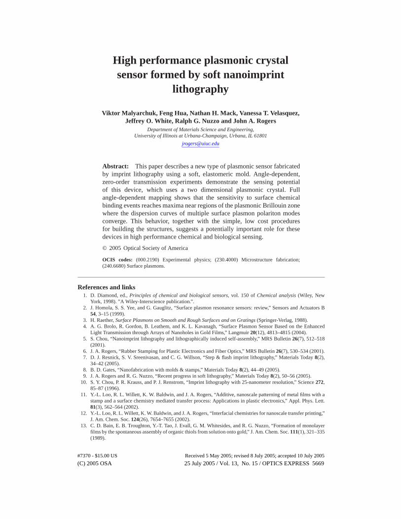
lithography in a serial fashion over limited areas with imperfect spatial coherence, or by expen-sive, advanced forms of projection mode photolithography. A simple, soft imprinting procedureillustrated in Figure 1 formed the structures used for the work described here. Casting and cur-
(a) (b) (c) (d)
Fig. 1. Plasmonic crystal fabrication process: (a) imprinting; (b) curing; (c) removing; and(d) gold deposition.
ing a prepolymer of poly(dimethylsiloxane) (PDMS) against a master of photoresist on a siliconwafer, patterned by projection mode deep ultraviolet lithography, formed the molds accordingto the following procedures. The master was first placed in a vacuum chamber along with100mL of (tridecafluoro-1,1,2,2-tetrahydrooctyl)-1-trichlorosilane (United Chemical Tech) for2 hours. The resulting silane layer prevents adhesion of the PDMS to the bare SiO2. Thestamp was prepared as a bilayer of hard PDMS (h-PDMS) to reproduce accurately the mas-ter’s features, and soft PDMS (s-PDMS) to provide a flexible support for the brittle h-PDMS.The h-PDMS (Gelest, Inc) was prepared as follows: 3.4g of poly(7-8% vinylmethylsiloxane)-(dimethylsiloxane), 100mg of (1,3,5,7-tetravinyl-1,3,5,7-tetramethylcyclotetrasiloxane) and50mg of platinum catalyst were mixed and placed in a vacuum chamber for 5 minutes. Af-ter removal from the chamber, 1g poly(25-30% methylhydrosiloxane)-(dimethylsiloxane) wasthen added, mixed and the resulting sample was placed back into vacuum for 5 minutes. Thisprepolymer mixture was spin cast onto the master at 1000rpm for 300s and then baked at 65◦Cfor 2 minutes. The s-PDMS (Sylgard 184, Dow Corning), prepared by mixing base and curingagent at a ratio of 10:1, was then poured onto the h-PDMS. The typical thicknesses used toconstruct the stamp were 10µm for the h-PDMS and 3mm for the s-PDMS. Baking at 65◦C for2 hours completed the curing of the polymers. Peeling the composite h-PDMS/s-PDMS replicaaway from the master completed the fabrication of a PDMS mold with the corresponding re-lief of the master. Many such molds can be produced from a single master, and each mold canbe used many times. In the first step of the imprinting procedure, a layer of a photocurablepolyurethane (PU) (NOA 73, Norland Products) was spin cast onto a glass slide (Fig. 1 (a)).Placing the PDMS mold into contact with this layer and then exposing it to ultraviolet light(350-380nm; long wavelength ultraviolet lamp, UVP) at∼19mW/cm2 for 1 hour through thetransparent mold cured the polyurethane into a solid form (Fig. 1 (b)). The resulting PU filmwas∼10µm thick and presented a relief structure in the geometry of the PDMS stamp. Remov-ing the mold (Fig. 1 (c)), completed the process. The imprinted polyurethane/glass substrateserved as a dielectric template for the production of a plasmonic crystal by blanket evaporationof a thin layer of gold (50nm) on top of a titanium adhesion layer (5nm). The gold layer wasselected to be sufficiently thin to enable operation in transmission mode but thick enough tosupport SPPs. These simple, low cost fabrication procedures are reliable, robust, and can beapplied over large areas. The resolution is exceptionally high; relief features as small as 1-2nmhave been successfully produced with this method [20].
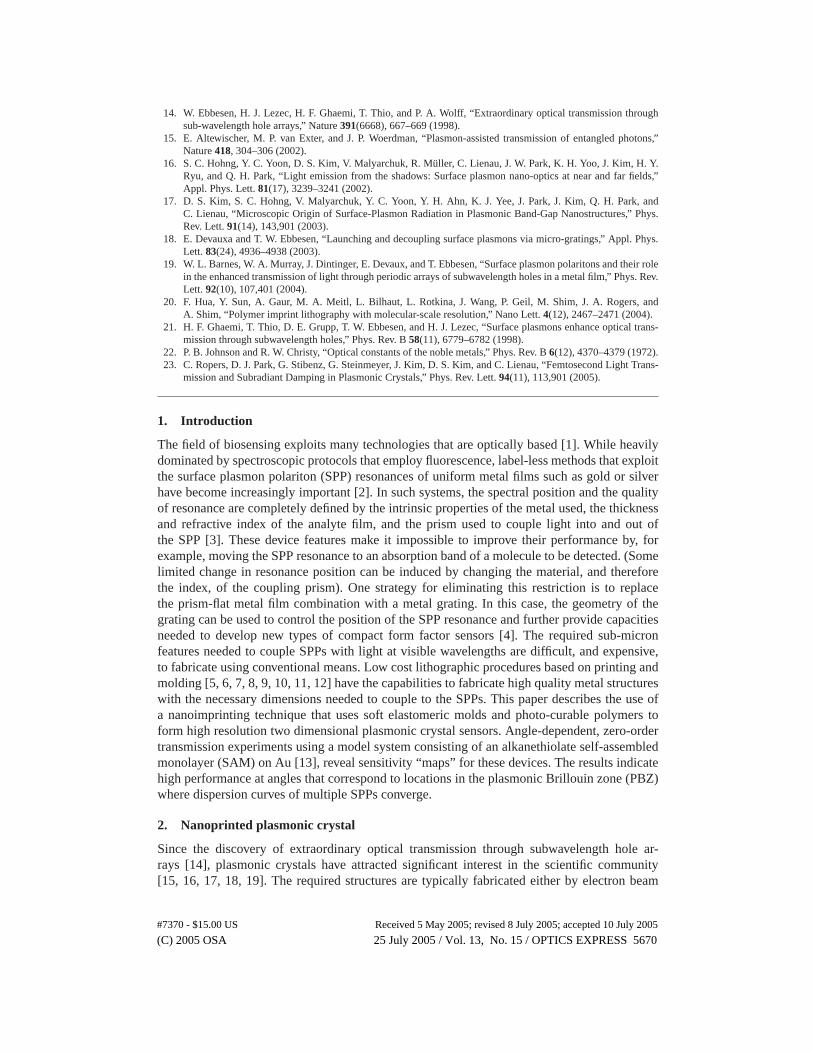
Figure 2 shows scanning electron micrographs of a typical device. The crystal used in thiswork has a square lattice consisting of depressions with diameters and depths of 545nm and300nm, respectively, and with a periodicity of 700nm. The walls of the depressions are notcoated with metal, due to the directional nature of the gold flux in the electron beam evaporationsystem that was used.
(C) 2005 OSA 25 July 2005 / Vol. 13, No. 15 / OPTICS EXPRESS 5671#7370 - $15.00 US Received 5 May 2005; revised 8 July 2005; accepted 10 July 2005
(a) (b) (c)
Fig. 2. Two dimensional plasmonic crystal sensor: (a) low resolution image; (b) scanningelectron micrograph (SEM); (c) high resolution SEM showing that walls of the depressionare free from metal.
The SPPs involve evanescent electromagnetic fields in the direction perpendicular tometal/dielectric interface. The depth of the depressions (300nm) is comparable to the SPP pene-tration depth into the dielectric medium. In such a geometry, our system consists of a plasmoniccrystal (continuous metallic layer on the upper surface) weakly coupled to an array of isolatedmetallic islands (bottom of the depressions).
3. Experiment and results
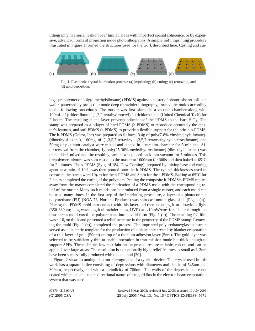
We performed zero-order transmission experiments in order to obtain the PBZ map of thesestructures [21, 16, 19]. The scheme of the setup is presented in Fig. 3. The sample was fixed
z x
θ
k
sam
pledetector
x x θk = |k| sin.
k
Fig. 3. Experimental zero-order transmission setup.
on a 2-axis rotation stage mounted inside of a UV-Vis-NIR spectrophotometer (Cary 5G). Oneaxis turned the device to the required polar angle of incidenceθ. The other rotated the samplearound the Z axis (Fig. 3). This stage defines the direction for excitation and propagation ofthe plasmonic modes on the metal surface. The transmission spectra have a nominal spectralresolution of 1nm, and are collected in a dual beam configuration to account for any intensityfluctuations in the light source.
PBZ maps were acquired by fixing the desired polar angle of incidence (θ) and recordinga transmission spectrum over a predefined wavelength range. The angleθ was varied between0◦ and 75◦ with incremented steps of 0.5◦. Two main directions inside PBZ were mapped. Onecorresponded to theΓ – X direction (sample rotated along the axis perpendicular to the gratingperiod), the other to theΓ – M direction (sample rotated around the axis perpendicular to thegrating diagonal).
The baseline for background correction was measured using the unstructured and uncoatedregion of the sample. The 50nm thick gold film was slightly transparent at a level consistentwith expectations for an unstructured film. In contrast, the plasmonic crystal shows strong res-onances in transmission intensity [14] that reach∼14% at the maximum and∼0.3% at theminimum for our sample at normal incidence. The overall tramsmission intensity decreases as
(C) 2005 OSA 25 July 2005 / Vol. 13, No. 15 / OPTICS EXPRESS 5672#7370 - $15.00 US Received 5 May 2005; revised 8 July 2005; accepted 10 July 2005
the polar angle (θ) increases and shows a value of∼5% at the maximum and∼0.3% at theminimum forθ = 75◦. This spectra are then used for PBZ mapping. The momentum of the SPPat theΓ-point in the PBZ isksppΓ = 0, at X,ksppX = π/p, and at M,ksppM = π/(d/2), wherepis the period of the grating andd its diagonal.
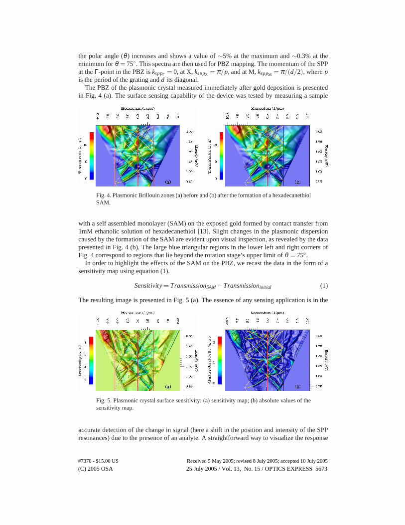
The PBZ of the plasmonic crystal measured immediately after gold deposition is presentedin Fig. 4 (a). The surface sensing capability of the device was tested by measuring a sample
Fig. 4. Plasmonic Brillouin zones (a) before and (b) after the formation of a hexadecanethiolSAM.
with a self assembled monolayer (SAM) on the exposed gold formed by contact transfer from1mM ethanolic solution of hexadecanethiol [13]. Slight changes in the plasmonic dispersioncaused by the formation of the SAM are evident upon visual inspection, as revealed by the datapresented in Fig. 4 (b). The large blue triangular regions in the lower left and right corners ofFig. 4 correspond to regions that lie beyond the rotation stage’s upper limit ofθ = 75◦.
In order to highlight the effects of the SAM on the PBZ, we recast the data in the form of asensitivity map using equation (1).
Sensitivity = TransmissionSAM −Transmissioninitial (1)
The resulting image is presented in Fig. 5 (a). The essence of any sensing application is in the
Fig. 5. Plasmonic crystal surface sensitivity: (a) sensitivity map; (b) absolute values of thesensitivity map.
accurate detection of the change in signal (here a shift in the position and intensity of the SPPresonances) due to the presence of an analyte. A straightforward way to visualize the response
(C) 2005 OSA 25 July 2005 / Vol. 13, No. 15 / OPTICS EXPRESS 5673#7370 - $15.00 US Received 5 May 2005; revised 8 July 2005; accepted 10 July 2005
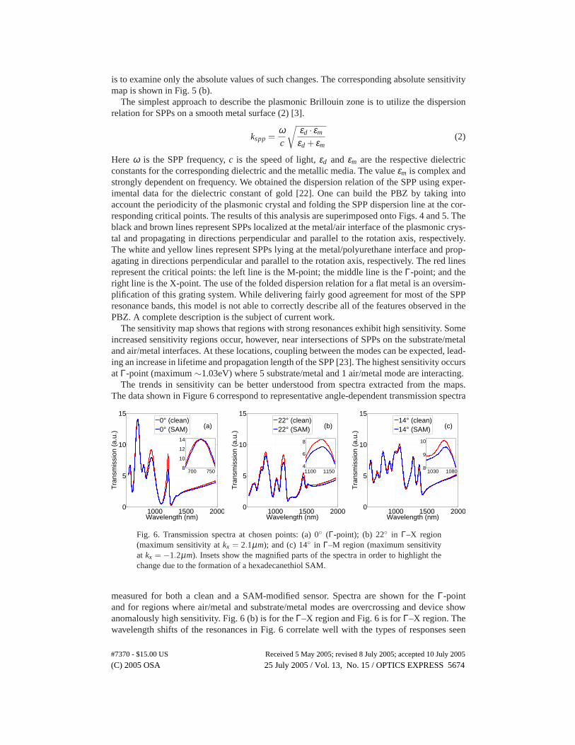
is to examine only the absolute values of such changes. The corresponding absolute sensitivitymap is shown in Fig. 5 (b).
The simplest approach to describe the plasmonic Brillouin zone is to utilize the dispersionrelation for SPPs on a smooth metal surface (2) [3].
kspp =ωc
√εd · εm
εd + εm(2)
Hereω is the SPP frequency,c is the speed of light,εd andεm are the respective dielectricconstants for the corresponding dielectric and the metallic media. The valueεm is complex andstrongly dependent on frequency. We obtained the dispersion relation of the SPP using exper-imental data for the dielectric constant of gold [22]. One can build the PBZ by taking intoaccount the periodicity of the plasmonic crystal and folding the SPP dispersion line at the cor-responding critical points. The results of this analysis are superimposed onto Figs. 4 and 5. Theblack and brown lines represent SPPs localized at the metal/air interface of the plasmonic crys-tal and propagating in directions perpendicular and parallel to the rotation axis, respectively.The white and yellow lines represent SPPs lying at the metal/polyurethane interface and prop-agating in directions perpendicular and parallel to the rotation axis, respectively. The red linesrepresent the critical points: the left line is the M-point; the middle line is theΓ-point; and theright line is the X-point. The use of the folded dispersion relation for a flat metal is an oversim-plification of this grating system. While delivering fairly good agreement for most of the SPPresonance bands, this model is not able to correctly describe all of the features observed in thePBZ. A complete description is the subject of current work.
The sensitivity map shows that regions with strong resonances exhibit high sensitivity. Someincreased sensitivity regions occur, however, near intersections of SPPs on the substrate/metaland air/metal interfaces. At these locations, coupling between the modes can be expected, lead-ing an increase in lifetime and propagation length of the SPP [23]. The highest sensitivity occursatΓ-point (maximum∼1.03eV) where 5 substrate/metal and 1 air/metal mode are interacting.
The trends in sensitivity can be better understood from spectra extracted from the maps.The data shown in Figure 6 correspond to representative angle-dependent transmission spectra
1000 1500 20000
5
10
15
Wavelength (nm)
Tra
nsm
issi
on (
a.u.
)
(a)0° (clean)0° (SAM)
700 7508
10
12
14
1000 1500 20000
5
10
15
Wavelength (nm)
Tra
nsm
issi
on (
a.u.
)
(b)22° (clean)22° (SAM)
1100 11504
6
8
1000 1500 20000
5
10
15
Wavelength (nm)
Tra
nsm
issi
on (
a.u.
)
(c)14° (clean)14° (SAM)
1030 10808
9
10
Fig. 6. Transmission spectra at chosen points: (a) 0◦ (Γ-point); (b) 22◦ in Γ–X region(maximum sensitivity atkx = 2.1µm); and (c) 14◦ in Γ–M region (maximum sensitivityat kx = −1.2µm). Insets show the magnified parts of the spectra in order to highlight thechange due to the formation of a hexadecanethiol SAM.
measured for both a clean and a SAM-modified sensor. Spectra are shown for theΓ-pointand for regions where air/metal and substrate/metal modes are overcrossing and device showanomalously high sensitivity. Fig. 6 (b) is for theΓ–X region and Fig. 6 is forΓ–X region. Thewavelength shifts of the resonances in Fig. 6 correlate well with the types of responses seen
(C) 2005 OSA 25 July 2005 / Vol. 13, No. 15 / OPTICS EXPRESS 5674#7370 - $15.00 US Received 5 May 2005; revised 8 July 2005; accepted 10 July 2005

in conventional SPR systems; these changes largely reflect a modest (∼4nm) red shifting ofthe position of the resonance due to the refractive index change at the dielectric/metal interfacethat results from the formation of the∼21A thick SAM [13] on the surface. The changes of therelative intensities of the different resonances, however, are are more unusual and may provideenhanced sensing capabilities. Models for analyzing these responses are the subject of ongoinginvestigations.
4. Conclusions
In conclusion, we have demonstrated the potential of soft imprinting technology for fabricatingplasmonic crystal sensors. Sensitivity maps of representative device were constructed fromangle-dependent transmission experiments. The sensors exhibit high sensitivity when operatedat certain angles. These angles correspond to locations in the plasmonic Brillouin zone wheredispersion curves of unperturbed SPP modes converge. This observation may be important forfuture classes of plasmonic crystal biosensors.
Acknowledgments
We acknowledge the support of the U.S. Department of Energy (DEFG02-91-ER45439). Allmeasurements reported here were carried out in the Laser and Spectroscopy Facility of the Fred-erick Seitz Materials Research Laboratory, University of Illinois, which is partially supportedby the U.S. Department of Energy under grant DEFG02-91-ER45439.
(C) 2005 OSA 25 July 2005 / Vol. 13, No. 15 / OPTICS EXPRESS 5675#7370 - $15.00 US Received 5 May 2005; revised 8 July 2005; accepted 10 July 2005


![Enhancing the Angular Sensitivity of Plasmonic Sensors ...biotheory.phys.cwru.edu/PDF/AOM.pdf · ultrasensitive plasmonic biosensors.[29,30] A plasmonic nanorod metamaterial (Type](https://img.pdfslide.net/doc/110x75/5fcdd2c6db367d06a677e7be/enhancing-the-angular-sensitivity-of-plasmonic-sensors-ultrasensitive-plasmonic.jpg)