Embed Size (px)
Citation preview
High Performance Power Delivery for
Nanoscale Integrated Circuits
by
Selcuk Kose
Submitted in Partial Fulfillment
of the
Requirements for the Degree
Doctor of Philosophy
Supervised by
Professor Eby G. Friedman
Department of Electrical and Computer Engineering
Arts, Sciences and Engineering
Edmund A. Hajim School of Engineering and Applied Sciences
University of Rochester
Rochester, New York
2012

ii
Dedication
This work is dedicated to the light of my life.

iii
Curriculum Vitae
Selcuk Kose received the B.S. degree
in electrical and electronics engineering
from Bilkent University, Ankara, Turkey,
in 2006, and the M.S. degree in electri-
cal and computer engineering from the
University of Rochester, Rochester, New
York, in 2008, where he is expected to
complete the Ph.D. degree in electrical engineering in 2012.
He worked as a part time engineer with the VLSI Design Center, Scientific and
Technological Research Council (TUBITAK), Ankara, Turkey, on low power ICs in
2006. During the summers of 2007 and 2008, he was with the Central Technology and
Special Circuits Team in the enterprise microprocessor division of Intel Corporation,
Santa Clara, California, where he was responsible for the functional verification of a
number of blocks in the clock network including the de-skew machine and optimization
iv
of the reference clock distribution network. In summer 2010, he interned in the
RF, Analog, and Sensor Group, Freescale Semiconductor, Tempe, Arizona, where he
developed design techniques and methodologies to reduce electromagnetic emissions.
His current research interests include the design and analysis of high performance
integrated circuits, monolithic DC-DC converters, and interconnect related issues
with specific emphasis on the design and analysis of power and clock distribution
networks, and 3-D integration.
Publications
Authored Book
1. R. Jakushokas, M. Popovich, A. V. Mezhiba, S. Kose, and E. G. Friedman,
Power Distribution Networks with On-Chip Decoupling Capacitors, Second Edi-
tion, Springer Publishers, 2011.
Journal Papers
2. S. Kose, S. Tam, S. Pinzon, B. McDermott, and E. G. Friedman, “Active Filter
Based Hybrid On-Chip DC-DC Converters for Point-of-Load Voltage Regula-
tion,” IEEE Transactions on Very Large Scale Integration (VLSI) Circuits (in
press).
3. S. Kose and E. G. Friedman, “Efficient Algorithms for Fast IR Drop Analysis
Exploiting Locality,” Integration, the VLSI Journal Vol. 45, No. 2, pp. 149-
161, March 2012.
4. S. Kose and E. G. Friedman, “Effective Resistance of a Two Layer Mesh,” IEEE
Transactions on Circuits and Systems II: Express Briefs, Vol. 58, No. 11, pp.
739-743, November 2011.
v
5. S. Kose, E. Salman, and E. G. Friedman, “Shielding Methodologies in the Pres-
ence of Power/Ground Noise,” IEEE Transactions on Very Large Scale Integra-
tion (VLSI) Circuits, Vol. 19, No. 8, pp. 1458-1468, August 2011.
6. I. Savidis, S. Kose, and E. G. Friedman, “Power Noise in TSV-Based 3-D Inte-
grated Circuits,” IEEE Journal of Solid-State Circuits (under review).
7. S. Kose and E. G. Friedman, “Distributed On-Chip Power Delivery,” IEEE
Journal on Emerging and Selected Topics in Circuits and Systems (under re-
view).
8. S. Kose, R. M. Secareanu, O. L. Hartin, and E. G. Friedman, “Current Profile
Estimation to Determine the Electromagnetic Emissions for a Broad Frequency
Range,” IEEE Transactions on Very Large Scale Integration (VLSI) Circuits
(in preparation).
Conference Papers
9. S. Kose, S. Tam, S. Pinzon, B. McDermott, and E. G. Friedman, “An Area
Efficient On-Chip Hybrid Voltage Regulator,” Proceedings of the IEEE Interna-
tional Symposium on Quality Electronic Design (ISQED), pp. 398-403, March
2012.
10. S. Kose and E. G. Friedman, “Fast Algorithms for IR Voltage Drop Analysis
Exploiting Locality,” Proceedings of the IEEE/ACM Design Automation Con-
ference (DAC), pp. 996-1001, June 2011.
11. S. Kose and E. G. Friedman, “Distributed Power Network Co-Design with On-
Chip Power Supplies and Decoupling Capacitors,” Proceedings of the ACM/IEEE
International Workshop on System Level Interconnect Prediction (SLIP), June
2011.
12. I. Savidis, S. Kose, and E. G. Friedman, “Power Grid Noise in TSV-Based
3-D Integrated Systems,” Government Microcircuit Applications and Critical
Technology Conference (GOMACHTech), pp. 129-132, March 2011.
13. S. Kose and E. G. Friedman, “Simultaneous Co-Design of Distributed On-Chip
vi
Power Supplies and Decoupling Capacitors,” Proceedings of the IEEE Interna-
tional SoC Conference (SOCC), pp. 15-18, September 2010.
14. S. Kose and E. G. Friedman, “An Area Efficient Fully Monolithic Hybrid Voltage
Regulator” Proceedings of the IEEE International Symposium on Circuits and
Systems (ISCAS), pp. 2718-2721, May/June 2010.
15. S. Kose and E. G. Friedman, “Fast Algorithms for Power Grid Analysis Based
on Effective Resistance,” Proceedings of the IEEE International Symposium on
Circuits and Systems (ISCAS), pp. 3661-3664, May/June 2010.
16. S. Kose and E. G. Friedman, “On-Chip Point-of-Load Voltage Regulator for
Distributed Power Supplies,” Proceedings of the ACM/IEEE Great Lakes Sym-
posium on VLSI (GLSVLSI), pp. 377-380, May 2010.
17. S. Kose, E. Salman, and E. G. Friedman, “Shielding Methodologies in the Pres-
ence of Power/Ground Noise,” Proceedings of the IEEE International Sympo-
sium on Circuits and Systems (ISCAS), pp. 2277-2280, May 2009.
18. S. Kose, E. Salman, Z. Ignjatovic, and E. G. Friedman, “Pseudo-Random Clock-
ing to Enhance Signal Integrity,” Proceedings of the IEEE International SoC
Conference (SOCC), pp. 47-50, September 2008.

vii
Acknowledgments
I would like to take this opportunity to thank the many individuals without whose
help and support this dissertation would not have been completed. First and fore-
most, I would like to thank my advisor, Professor Eby G. Friedman, for his support,
guidance, and encouragement during each and every step of my Ph.D. study. It was
a great pleasure for me to accomplish my thesis work under his supervision. What I
know today about the process of research, I learned from Professor Eby G. Friedman.
I would also like to thank Professor Mehmet Kemal Aktas, Professor Mark F.
Bocko, Professor Sandhya Dwarkadas, Professor Zeljko Ignjatovic, and Professor En-
gin Ipek for serving on my proposal and defense committees. Your insightful com-
ments, critical reviews, and helpful advice enhanced my research and filled important
gaps in my thesis dissertation. I would like to give my sincerest gratitude to Dr. Simon
Tam, Dr. Justin Leung, and Stefan Rusu from Intel Corporation for their guidance
and support during my two summer internships. I would also like to express my
warm thanks to Dr. Radu M. Secareanu and Dr. Olin L. Hartin from Freescale
Semiconductor for their guidance during my internship at Freescale Semiconductor.

viii
Sally Pinzon, Bruce McDermott, Matthew Pace, Paul Perez, Dave Bishop, Dave
Sackett, and Michael Guidash from Eastman Kodak offered their experience and the
necessary equipment during the design, fabrication, and test of the on-chip voltage
regulator. Thank you all.
I was fortunate to do my graduate work with a group of talented and helpful
students. I would like to thank previous and current members of the High Perfor-
mance Integrated Circuits Laboratory: Dr. Vasilis Pavlidis, Prof. Emre Salman, Dr.
Jonathan Rosenfeld, Dr. Renatas Jakushokas, Ioannis Savidis, Ravi Patel, Inna Vais-
band, Boris Vaisband, and Alexander Shapiro. I thank RuthAnn Williams for her
endless efforts on my behalf, allowing me to focus my time on my research. I would
also like to acknowledge the staff of the Department of Electrical and Computer
Engineering for their assistance and support.
I would like to thank my bosom friend, Esat Belviranli, who is always as close as
a phone call. I would also like to thank my father Nurettin Kose and mother Gulsum
Kose for their continued support, encouragement, and motivation. They deserve more
credit than I do for each and every success I have in my life. Thank you for the many
sacrifices you made to ensure my success. Lastly, I would like to thank my love, best
friend, and wife, Leman Kose, who knows my stories, gets my jokes, warms my heart,
finishes my sentences, and soothes my worries!

ix
Abstract
A critical challenge in high performance nanoscale integrated circuits is high qual-
ity power delivery. The efficient generation and distribution of multiple on-chip power
supply voltages require fundamental changes to the power delivery process to provide
increased current in next generation nanoscale integrated circuits. Four primary com-
ponents are required to realize an efficient power delivery system: (a) ultra-small volt-
age converters to generate power close to the load, (b) accurate models to characterize
the individual power components, (c) efficient algorithms to analyze the quality of
the power delivered to the load circuits, and (d) a co-design methodology to simulta-
neously determine the optimal location of the on-chip power supplies and decoupling
capacitors.
In this dissertation, a hybrid combination of a switching and low-dropout (LDO)
regulator as a point-of-load power supply for next generation heterogeneous systems is
proposed. The area of this circuit is significantly smaller than the area of conventional
voltage regulators, while maintaining high current efficiency. The proposed circuit

x
provides a means for distributing multiple local power supplies across an integrated
circuit.
Another important challenge in the realization of effective power delivery systems
is the analysis of this highly complicated structure where individual voltage fluctua-
tions at millions of nodes need to be efficiently determined. Closed-form expressions
for the effective resistance between circuit components have been developed. This
effective resistance model is utilized in the development of a power grid analysis algo-
rithm to compute the node voltages without requiring any iterations. This algorithm
drastically improves computational complexity since the iterative procedures to de-
termine IR drop and L di/dt noise are no longer needed.
With the introduction of ultra-small on-chip voltage regulators, there is a need for
novel design methodologies to determine the location of these on-chip power supplies
and decoupling capacitors. A co-design methodology is proposed to simultaneously
determine the optimal location of the power supplies and decoupling capacitors within
a high performance power delivery network. Optimization algorithms widely used for
facility location problems are applied in the proposed methodology. The effects of
the size, number, and location of the power supplies and decoupling capacitors on the
power noise are also discussed.

xi
Contents
Dedication ii
Curriculum Vitae iii
Acknowledgments vii
Abstract ix
List of Tables xvii
List of Figures xix
Foreword 1
1 Introduction 4
1.1 Power Delivery . . . . . . . . . . . . . . . . . . . . . . . . . . . . . . 10
1.2 Proposal Outline . . . . . . . . . . . . . . . . . . . . . . . . . . . . . 12
xii
2 On-Chip Power Generation and Distribution 15
2.1 On-Chip Power Supply Design . . . . . . . . . . . . . . . . . . . . . . 17
2.1.1 Linear Voltage Regulators . . . . . . . . . . . . . . . . . . . . 17
2.1.2 Switching Voltage Regulators . . . . . . . . . . . . . . . . . . 21
2.1.3 Switched-Capacitor Voltage Regulators . . . . . . . . . . . . . 24
2.1.4 A Comparison of Voltage Regulators for On-Chip Integration . 26
2.2 On-Chip Power Distribution Networks . . . . . . . . . . . . . . . . . 28
2.2.1 Decoupling Capacitors . . . . . . . . . . . . . . . . . . . . . . 29
2.2.2 Hierarchical Power Distribution Networks with
Decoupling Capacitors . . . . . . . . . . . . . . . . . . . . . . 32
2.2.3 On-Chip Decoupling Capacitors . . . . . . . . . . . . . . . . . 34
2.2.4 On-Chip Power Distribution Networks . . . . . . . . . . . . . 39
2.3 Summary . . . . . . . . . . . . . . . . . . . . . . . . . . . . . . . . . 46
3 Power Noise Analysis 48
3.1 Power Network Modeling and Analysis . . . . . . . . . . . . . . . . . 49
3.1.1 Models of Power Distribution Networks . . . . . . . . . . . . . 49
3.1.2 Analysis of Power Distribution Networks . . . . . . . . . . . . 52
3.2 Summary . . . . . . . . . . . . . . . . . . . . . . . . . . . . . . . . . 63
4 An Ultra-Small Hybrid Voltage Regulator 65
xiii
4.1 Active Filter Based Switching DC-DC Converter Design . . . . . . . 69
4.1.1 Active Filter Design . . . . . . . . . . . . . . . . . . . . . . . 71
4.1.2 Op Amp Design . . . . . . . . . . . . . . . . . . . . . . . . . . 74
4.2 Pros and Cons of Active Filter-Based Voltage Regulator . . . . . . . 76
4.3 Experimental Results . . . . . . . . . . . . . . . . . . . . . . . . . . . 78
4.4 On-chip Point-of-Load Voltage Regulation . . . . . . . . . . . . . . . 87
4.5 Summary . . . . . . . . . . . . . . . . . . . . . . . . . . . . . . . . . 89
5 Effective Resistance in a Two Layer Mesh 90
5.1 Kirchhoff’s Current Law Revisited . . . . . . . . . . . . . . . . . . . . 94
5.2 Separation of Variables . . . . . . . . . . . . . . . . . . . . . . . . . . 96
5.3 Effective Resistance between Two Nodes . . . . . . . . . . . . . . . . 99
5.4 Closed-Form Expression of the Effective Resistance . . . . . . . . . . 100
5.5 Experimental Results . . . . . . . . . . . . . . . . . . . . . . . . . . . 102
5.6 Summary . . . . . . . . . . . . . . . . . . . . . . . . . . . . . . . . . 105
6 Fast Algorithms For IR Voltage Drop Analysis 106
6.1 Analytic IR Drop Analysis . . . . . . . . . . . . . . . . . . . . . . . . 108
6.1.1 One power supply and one current load . . . . . . . . . . . . . 110
6.1.2 One power supply and multiple current loads . . . . . . . . . . 112
6.1.3 Multiple power supplies and one current load . . . . . . . . . 114

xiv
6.1.4 Multiple power supplies and multiple current loads . . . . . . 117
6.2 Locality in Power Grid Analysis . . . . . . . . . . . . . . . . . . . . . 120
6.2.1 Principle of spatial locality in a power grid . . . . . . . . . . . 121
6.2.2 Effect of spatial locality on computational complexity . . . . . 124
6.2.3 Exploiting spatial locality in the proposed method . . . . . . . 126
6.2.4 Error correction windows . . . . . . . . . . . . . . . . . . . . . 128
6.3 Experimental Results . . . . . . . . . . . . . . . . . . . . . . . . . . . 130
6.4 Summary . . . . . . . . . . . . . . . . . . . . . . . . . . . . . . . . . 137
7 Shielding Methodologies in the Presence of Power/Ground Noise 139
7.1 Background . . . . . . . . . . . . . . . . . . . . . . . . . . . . . . . . 142
7.1.1 Crosstalk Noise Reduction Techniques . . . . . . . . . . . . . 142
7.1.2 Coupled Interconnect Model and Decision Criterion . . . . . . 145
7.1.3 Power/Ground Noise Model . . . . . . . . . . . . . . . . . . . 149
7.2 Effects of Technology and Design Parameters on the Crosstalk Noise
Voltage . . . . . . . . . . . . . . . . . . . . . . . . . . . . . . . . . . . 151
7.2.1 Effect of Technology Scaling on the Crosstalk Noise Voltage . 152
7.2.2 Effect of Line Length on Crosstalk Noise . . . . . . . . . . . . 156
7.2.3 Effect of Shield Line Width on Crosstalk Noise . . . . . . . . . 159
7.2.4 Effect of Rline/Rs on Crosstalk Noise . . . . . . . . . . . . . . 159
xv
7.2.5 Effect of the Ratio of Substrate Capacitance to Coupling Ca-
pacitance on Crosstalk Noise . . . . . . . . . . . . . . . . . . . 162
7.2.6 Effect of Self- and Mutual Inductance on Crosstalk Noise . . . 164
7.2.7 Effect of Distance between Aggressor and Victim Lines on Crosstalk
Noise . . . . . . . . . . . . . . . . . . . . . . . . . . . . . . . . 166
7.3 Shield Insertion or Physical Spacing in a Noisy Environment . . . . . 167
7.4 Summary . . . . . . . . . . . . . . . . . . . . . . . . . . . . . . . . . 171
8 Distributed On-Chip Power Delivery 172
8.1 Point-of-Load Voltage Regulators . . . . . . . . . . . . . . . . . . . . 176
8.2 Facility Location Problem . . . . . . . . . . . . . . . . . . . . . . . . 176
8.3 Proposed Optimization Methodology . . . . . . . . . . . . . . . . . . 180
8.4 Case Study and Benchmark Circuits . . . . . . . . . . . . . . . . . . 185
8.5 Discussion . . . . . . . . . . . . . . . . . . . . . . . . . . . . . . . . . 196
8.6 Summary . . . . . . . . . . . . . . . . . . . . . . . . . . . . . . . . . 198
9 Future Work 200
9.1 Effective Impedance within a Power Grid . . . . . . . . . . . . . . . . 201
9.2 Transient Power Grid Analysis Based on Closed-Form Expressions . . 203
9.3 Power and Clock Network Co-Design . . . . . . . . . . . . . . . . . . 204
9.4 Summary . . . . . . . . . . . . . . . . . . . . . . . . . . . . . . . . . 205
xvi
10 Conclusions 206
Bibliography 211
Appendices
A Derivation of R2(x,y) 236
B Closed-Form Expressions for Interconnect Resistance, Capacitance,
and Inductance 239

xvii
List of Tables
2.1 Comparison of different voltage regulators . . . . . . . . . . . . . . . 27
4.1 Sensitivity of a third order Sallen-Key filter . . . . . . . . . . . . . . 74
4.2 Performance comparison among different DC-DC converters . . . . . 85
5.1 Closed-form effective resistance expressions . . . . . . . . . . . . . . . 102
5.2 Accuracy of the effective resistance model . . . . . . . . . . . . . . . 103
5.3 Error induced by the infinite grid approximation . . . . . . . . . . . . 104
6.1 Error of Algorithm I as compared to SPICE . . . . . . . . . . . . . . 131
6.2 Error of Algorithm II as compared to SPICE . . . . . . . . . . . . . . 131
6.3 Error of Algorithm of III as compared to SPICE . . . . . . . . . . . . 132
6.4 Error of Algorithm IV without error correction . . . . . . . . . . . . . 133
6.5 Error of Algorithm IV with error correction . . . . . . . . . . . . . . 134
6.6 Performance comparison . . . . . . . . . . . . . . . . . . . . . . . . . 136
xviii
7.1 Interconnect parameters for 65 nm, 45 nm, and 32 nm technology nodes149
7.2 Effect of technology and design parameters on the resistance, capaci-
tance, and inductance of the interconnect . . . . . . . . . . . . . . . . 152
7.3 Critical line length and driver resistance for several technology nodes 158
7.4 Decision criterion for the critical interconnect length and width . . . 170
8.1 Definition of the parameters in (8.1)-(8.8). . . . . . . . . . . . . . . . 184
8.2 Properties of ISPD benchmark circuits . . . . . . . . . . . . . . . . . 191
8.3 Five different power supply and decoupling capacitor arrangements. . 191
8.4 Optimum location of power supplies and decoupling capacitors that
minimize the average voltage drop for superblue5. . . . . . . . . . . . 192
8.5 Optimum location of power supplies and decoupling capacitors that
minimize the average voltage drop for superblue10. . . . . . . . . . . 193
8.6 Optimum location of power supplies and decoupling capacitors that
minimize the average voltage drop for superblue12. . . . . . . . . . . 194
8.7 Optimum location of power supplies and decoupling capacitors that
minimize the average voltage drop for superblue18. . . . . . . . . . . 195
8.8 Maximum and average voltage drop with 1 volt power supply voltage
without any increase in area. . . . . . . . . . . . . . . . . . . . . . . . 197

xix
List of Figures
1.1 NY Times article about the first transistor. . . . . . . . . . . . . . . . 5
1.2 Structure of a FET from the first transistor patent. . . . . . . . . . . 6
1.3 Evolution of integrated circuits. . . . . . . . . . . . . . . . . . . . . . 7
1.4 A simplified model for a power distribution network. . . . . . . . . . 9
2.1 Evolution of the average power supply . . . . . . . . . . . . . . . . . 16
2.2 Evolution of the power supply voltage . . . . . . . . . . . . . . . . . . 17
2.3 Evolution of the current supply . . . . . . . . . . . . . . . . . . . . . 18
2.4 Basic linear voltage regulator . . . . . . . . . . . . . . . . . . . . . . 19
2.5 A basic buck converter . . . . . . . . . . . . . . . . . . . . . . . . . . 22
2.6 A basic switched-capacitor step-up voltage converter . . . . . . . . . 25
2.7 Hierarchical power distribution network . . . . . . . . . . . . . . . . . 28
2.8 Target impedance per computer generation . . . . . . . . . . . . . . . 30
2.9 Ideal and practical decoupling capacitors . . . . . . . . . . . . . . . . 31

xx
2.10 Impedance of a hierarchical power distribution network . . . . . . . . 32
2.11 Structure of an n-type MOS capacitor . . . . . . . . . . . . . . . . . . 36
2.12 MOSFET capacitance in different regions of operation . . . . . . . . 37
2.13 Charge distribution of a MOS capacitor within accumulation . . . . . 37
2.14 Charge distribution of a MOS capacitor within depletion . . . . . . . 38
2.15 Charge distribution of a MOS capacitor within inversion . . . . . . . 38
2.16 Routed and mesh power/ground distribution networks . . . . . . . . 41
2.17 Power/ground grid structure for high performance integrated circuits 42
2.18 Wire-bond packaging . . . . . . . . . . . . . . . . . . . . . . . . . . . 43
2.19 Flip-chip packaging . . . . . . . . . . . . . . . . . . . . . . . . . . . . 45
3.1 Power grid model . . . . . . . . . . . . . . . . . . . . . . . . . . . . . 50
3.2 Triangular current activity model . . . . . . . . . . . . . . . . . . . . 51
3.3 Hierarchical power grid analysis . . . . . . . . . . . . . . . . . . . . . 57
3.4 Mapping of a fine power grid onto a coarse power grid . . . . . . . . . 59
3.5 A resistive grid and corresponding random walk game . . . . . . . . . 62
4.1 Proposed DC-DC voltage converter . . . . . . . . . . . . . . . . . . . 70
4.2 Low pass Sallen-Key filter . . . . . . . . . . . . . . . . . . . . . . . . 72
4.3 Three stage Op Amp for the proposed voltage regulator . . . . . . . . 75
4.4 Phase margin of the Op Amp . . . . . . . . . . . . . . . . . . . . . . 76
4.5 Die microphotograph of the hybrid voltage regulator . . . . . . . . . 78

xxi
4.6 Set-up for load transient testing . . . . . . . . . . . . . . . . . . . . . 80
4.7 Test board and circuit . . . . . . . . . . . . . . . . . . . . . . . . . . 80
4.8 Measured transient response of the proposed voltage regulator . . . . 81
4.9 Measured load regulation . . . . . . . . . . . . . . . . . . . . . . . . . 84
4.10 Output DC voltage shift . . . . . . . . . . . . . . . . . . . . . . . . . 86
4.11 Representative power delivery system . . . . . . . . . . . . . . . . . . 87
5.1 Two layer orthagonal metal lines connected with vias . . . . . . . . . 92
5.2 Superposition within an infinite mesh structure . . . . . . . . . . . . 94
6.1 Simplified power grid models . . . . . . . . . . . . . . . . . . . . . . . 109
6.2 Power grid model for Algorithm I . . . . . . . . . . . . . . . . . . . . 111
6.3 Pseudo-code of Algorithm I . . . . . . . . . . . . . . . . . . . . . . . 112
6.4 Power grid model for Algorithm II . . . . . . . . . . . . . . . . . . . . 113
6.5 Pseudo-code of Algorithm II . . . . . . . . . . . . . . . . . . . . . . . 114
6.6 Power grid model for Algorithm III . . . . . . . . . . . . . . . . . . . 115
6.7 Pseudo-code of Algorithm III . . . . . . . . . . . . . . . . . . . . . . 118
6.8 Power grid model for Algorithm IV . . . . . . . . . . . . . . . . . . . 119
6.9 Pseudo-code of Algorithm IV . . . . . . . . . . . . . . . . . . . . . . 121
6.10 Power grid model with C4 bumps . . . . . . . . . . . . . . . . . . . . 123
6.11 Per cent current provided to current load L1 . . . . . . . . . . . . . . 124
6.12 Per cent current provided to current load L2 . . . . . . . . . . . . . . 125

xxii
6.13 Error induced by the infinite grid assumption . . . . . . . . . . . . . 125
6.14 Proposed power grid partitioning . . . . . . . . . . . . . . . . . . . . 126
6.15 Illustration of error correction windows . . . . . . . . . . . . . . . . . 129
7.1 Global interconnect model . . . . . . . . . . . . . . . . . . . . . . . . 142
7.2 2π RLC interconnect model . . . . . . . . . . . . . . . . . . . . . . . 145
7.3 Noisy ground network utilized as a shield line . . . . . . . . . . . . . 146
7.4 Crosstalk noise with a noisy shield line and a noise free shield line . . 150
7.5 Crosstalk noise at the sense node as the P/G noise is varied . . . . . 153
7.6 Crosstalk noise at the sense node for several technology nodes . . . . 154
7.7 Crosstalk noise at the sense node for several driver sizes . . . . . . . . 155
7.8 Crosstalk noise occurring at the sense node for physical spacing and
shield insertion . . . . . . . . . . . . . . . . . . . . . . . . . . . . . . 157
7.9 Effect of shield line width on crosstalk noise for a 1 mm interconnect line160
7.10 Effect of Rline/Rs on crosstalk noise . . . . . . . . . . . . . . . . . . . 161
7.11 Effect of substrate and coupling capacitances on crosstalk noise for 0.5
mm line . . . . . . . . . . . . . . . . . . . . . . . . . . . . . . . . . . 163
7.12 Effect of substrate and coupling capacitances on crosstalk noise for 1
mm line . . . . . . . . . . . . . . . . . . . . . . . . . . . . . . . . . . 164
7.13 Effect of self- and mutual inductance on crosstalk noise . . . . . . . . 165
7.14 Effect of physical spacing on crosstalk noise . . . . . . . . . . . . . . 167

xxiii
7.15 Case study: crosstalk noise at the sense node for 0.5 mm line . . . . . 168
7.16 Case study: crosstalk noise at the sense node for 1 mm line . . . . . . 169
8.1 Next generation power delivery network . . . . . . . . . . . . . . . . . 174
8.2 Microphotograph of an ultra-small voltage regulator . . . . . . . . . . 177
8.3 Large scale electric power distribution system . . . . . . . . . . . . . 178
8.4 Floorplan of example circuits . . . . . . . . . . . . . . . . . . . . . . 188
8.5 Map of voltage drops for two example circuits . . . . . . . . . . . . . 189
8.6 Floorplan of ISPD’11 circuits . . . . . . . . . . . . . . . . . . . . . . 190
8.7 Map of voltage drops within superblue5 . . . . . . . . . . . . . . . . . 192
8.8 Map of voltage drops within superblue10 . . . . . . . . . . . . . . . . 193
8.9 Map of voltage drops within superblue12 . . . . . . . . . . . . . . . . 194
8.10 Map of voltage drops within superblue18 . . . . . . . . . . . . . . . . 195
9.1 Power grid model for transient analysis . . . . . . . . . . . . . . . . . 202

1
Foreword
The author, Selcuk Kose, has developed all of the design and analysis methodolo-
gies, derived the closed-form models, and evaluated all of the results described in this
Ph.D. dissertation. The introduction (Chapter 1) and background chapters (Chap-
ters 2 and 3) are based on the academic literature, presented by other researchers.
Other contributions from colleagues are listed below.
Chapter 4: S. Kose is the primary author of this chapter, which has recently been
accepted for publication in the IEEE Transactions on Very Large Scale Integration
(VLSI) Systems. The development and evaluation of the research have been per-
formed with the co-author of the paper, my Ph.D. advisor, E. G. Friedman. This
research has also been conducted in collaboration with co-authors S. Tam from In-
tel Corporation and, S. Pinzon and B. McDermott from Eastman Kodak Company.
Part of this work has also been published in the Proceedings of the IEEE Interna-
tional Symposium on Circuits and Systems, Proceedings of the ACM/IEEE Great
Lakes Symposium on VLSI, and Proceedings of the IEEE International Symposium

2
on Quality Electronic Design.
Chapter 5: S. Kose is the primary author of this chapter, which has been pub-
lished in the IEEE Transactions on Circuits and Systems II: Express Briefs. The
development and evaluation of the research have been performed with the co-author
of the paper, E. G. Friedman.
Chapter 6: S. Kose is the primary author of this chapter, which has been published
in Integration, the VLSI Journal. The development and evaluation of the research
have been performed with the co-author, E. G. Friedman. Part of this work has also
been published in the Proceedings of the IEEE International Symposium on Circuits
and Systems and Proceedings of the ACM/IEEE International Design Automation
Conference with the aforementioned co-author.
Chapter 7: S. Kose is the primary author of this chapter, which has been published
in the IEEE Transactions on Very Large Scale Integration (VLSI) Systems. The
development and evaluation of the research have been performed with the co-authors,
E. Salman and E. G. Friedman. Part of this work has also been published in the
Proceedings of the IEEE International Symposium on Circuits and Systems with the
aforementioned co-authors.
Chapter 8: S. Kose is the primary author of this chapter, which has been submit-
ted for publication to the IEEE Journal on Emerging and Selected Topics in Circuits
and Systems. The development and evaluation of the research have been performed

3
with the co-author, E. G. Friedman. Part of this work has been published in the Pro-
ceedings of the IEEE Intenational SoC Conference and Proceedings of the ACM/IEEE
International Workshop on System level Interconnect Prediction (SLIP).

4
Chapter 1
Introduction
A small article on the back page of The New York Times on July 1st, 1948 an-
nounced the first transistor shortly after Bell Labs presented the invention of the
first point-contact transistor at a press conference. This article, shown in Fig. 1.1,
appeared in the last page of the newspaper without much to say about the device.
At that time, people could not anticipate the broad social impact that this invention
would produce.
J. E. Lilienfeld invented and patented the concept of a field effect transistor (FET)
in 1926 [1]. An illustration of the structure of a field effect transistor from this patent
is shown in Fig. 1.2. Note that the structure is quite similar to that of a modern
highly scaled metal-oxide-semiconductor (MOS) FET [2]. Despite receiving the first
transistor patent, Lilienfeld could not physically manufacture and test an actual tran-
sistor. The first transistor was fabricated by J. Bardeen and W. Brattain of Bell Labs
twenty years later in 1947 [3]. Over the next two months, W. Shockley of Bell Labs

5
Figure 1.1: The New York Times article about the first transistor on July 1st, 1948.The word ‘transistor’ appeared in a printed article for the first time, according to theOxford English Dictionary.
developed the basic expressions characterizing the bipolar junction transistor (BJT),
a result of fundamental significance as was the fabrication of the first transistor by
Bardeen and Brattain [4]. Brattain, Bardeen, and Shockley received the Nobel price
in Physics “for their researches on semiconductors and their discovery of the transis-
tor effect” in 1956. Unfortunately, this fundamental research result of producing the
first transistor failed to give any credit to Lilienfeld’s early work [5].
The invention of the transistor greatly benefited from research on quantum me-
chanics during the 1920’s since a thorough understanding of solid state physics and
6
Figure 1.2: Structure of a field effect transistor (FET) from Lilienfend’s patent“Method and Apparatus for Controlling Electric Currents,” U.S. No. 1,745,175 in1926. This patent is the first patent to describe an FET to achieve amplification bychanging the conductivity of a poorly conducting material (a semiconductor).
electronic band structure requires a deep understanding of quantum mechanics. Re-
search on solid-state devices continued in the 50’s and 60’s at an accelerated pace.
The first FET was fabricated by D. Kahng after joining Bell Labs in 1959 [6]. In
1958, the first integrated circuit consisting of both passive and active components
was fabricated at Texas Instruments by Jack Kilby using gold wire interconnections
on a single germanium substrate, as illustrated in Fig. 1.3a.
Although bipolar junction transistor (BJT) technology was more advanced as com-
pared to MOS technology when MOSFETs were first fabricated, MOSFET technology
in the early 1980’s demonstrated two primary advantages over BJT technology. With
an increasing number of transistors integrated onto a single monolithic substrate,
production cost had become a primary limiting factor. MOSFET fabrication requires
fewer processing steps than BJT technology, resulting in a lower production cost.
7
(a) (b)
Figure 1.3: Evolution of integrated circuits. (a) First integrated circuit on a singlegermanium substrate with gold wire interconnections by Jack Kilby in 1958 and (b)Intel 8 core microprocessor Nehalem-Ex with over 2.3 billion transistors on a singledie in 2010.
Additionally, MOSFETs can be scaled without significant performance degradation.
With scaling, MOSFET technology requires less power and can operate at higher
speeds. Alternatively, the operational characteristics of BJTs degrade with scaling.
Complementary MOSFET (CMOS) technology was invented by Wanlass and Sah
in 1963 [7]. Due to significantly lower static power consumption as compared to
equivalent BJT, PMOS, and NMOS counterparts, CMOS logic has become the basis
for a wide range of modern integrated circuits. With scaling, MOSFET technology
has become the technology of choice. The number of transistors on a single die has
fundamentally increased with scaling. G. Moore of Fairchild Semiconductor stated in
his renowned paper [8] that

8
“The complexity for minimum component costs has increased at a rate
of roughly a factor of two per year... Over the longer term, the rate of
increase is a bit more uncertain, although there is no reason to believe it
will not remain nearly constant for at least 10 years. That means by 1975,
the number of components per integrated circuit for minimum cost will be
65,000. I believe that such a large circuit can be built on a single wafer.”
– G. Moore, 1965 [8]
Moore’s law has proven to be correct not only until 1975 but to today. Modern
integrated circuits now contain billions of transistor and provide more and more
functionality on a single die. A 2.3 billion transistor eight core processor with 24 MB
of cache has recently been developed in a 45 nm CMOS technology by Intel [9], and
a microphotograph is shown in Fig. 1.3b. The die size of this microprocessor is 684
mm2.
With continuous technology scaling, more functionality can be incorporated on-
chip, increasing the number of transistors and die area. The power consumption also
increases with the number of on-chip components, placing more stringent constraints
on the power delivery process. A greater number of transistors increases the total
current provided by the power distribution network. Shorter transition times, smaller
noise margins, and increased current densities further complicate both power gener-
ation and distribution. Due to the parasitic resistance and inductance of the power
9
Rp Lp
LgRg
V=Vdd
V=Vgnd
ddV=V − IR − L dI/dtpp
gndV=V + IR + L dI/dtgg
SupplyPower
Iload(t)
Iload(t)
Iload(t)
LoadCircuit
Figure 1.4: Simplified model of a power distribution network. Due to the finiteparasitic impedance between the power supply and load circuitry, voltage drops andbounces can occur.
distribution network, resistive IR [10–13] and inductive L di/dt [14–16] voltage drops
are produced within the power distribution network, as schematically illustrated in
Fig. 1.4. With technology scaling, the interconnect wire width and thickness decrease
in the lower metal layers, further increasing the voltage drop.
To overcome these challenges and deliver a clean supply voltage to the active
devices, one or multiple robust power supplies and a low impedance power distribution
network between the power supplies and load circuitry are required. An overview of
power delivery in high performance integrated circuits is discussed in Section 1.1. An
outline of this research proposal is presented in Section 1.2.

10
1.1 Power Delivery
Historically, power supplies, which provide current to the on-chip active circuits,
are placed off-chip and connected to the on-chip circuitry via input/output (I/O)
pads. Large passive components (inductors and capacitors) are used in these off-
chip power supplies. The size of the power supplies is large and a significant portion
of the power is dissipated by the interconnections between the power supply and
load circuits [17, 18]. The power dissipated by the interconnections and I/O pads
is significant when a greater number of transistor is placed on-chip, increasing the
overall current demand [19]. Additionally, die area has grown about 14% per year
from 1971 to 1995 [20–22], also increasing the total consumed power. Scaling CMOS
has greatly lowered the power loss among the off-chip interconnect and I/O pads.
Another issue with off-chip power supplies is the number of dedicated I/O pads
for power and ground connections. For example, a package for a 65 nm dual core
processor requires 604 pins, of which 238 are signal pins and the remaining 366 pins
(60% of the total number of pins) are dedicated to power and ground [23]. Reducing
the number of dedicated power and ground pins becomes of greater significance with
the integration of more functional blocks onto a single integrated circuit. Additionally,
power consumption is significantly reduced with the monolithic integration of the
power supply.
The on-chip power supply will therefore a) minimize parasitic losses since the

11
power supply is closer to the load circuitry [18], b) provide a cleaner supply voltage
to the load circuitry due to the reduced parasitic impedance between the power sup-
ply and the load circuitry, c) reduce the number of dedicated I/O pins for power and
ground [22], d) provide fast line and load regulation during abrupt changes to the in-
put voltage or output current demand [24], and e) simplify the application of dynamic
voltage frequency scaling (DVFS) techniques [25]. The development of on-chip power
supplies, however, is not a straightforward issue. One primary limitation of on-chip
power supplies is the large area requirement. Different circuit topologies have been
proposed over the past two decades to reduce the size of the on-chip power supplies
while maintaining high efficiency and fast load regulation [22, 24, 26–31]. With the
introduction of low area on-chip power supplies, multiple power supplies can now
be integrated on-chip to generate voltages closer to the load circuits while lowering
parasitic losses.
When a clean power supply is generated, a power and ground (P/G) network
distributes this voltage to the load circuitry. Due to the parasitic impedance of the
P/G network, the voltage delivered to the load circuitry is different from the supply
voltage, as illustrated in Fig. 1.4. Quantifying these voltage changes due to P/G
noise in power distribution networks is essential in providing correct operation and
high performance. With the continuous increase in the number of transistors and
die area, P/G network analysis has become an increasingly challenging task. The

12
analysis process is further complicated by the increase in the number of on-chip power
supplies. Different techniques have been proposed to quickly and accurately analyze
P/G networks.
Analysis of the power network is also important due to crosstalk among adjacent
interconnect lines [32]. Inserting shield lines between aggressor and victim lines is
often done to reduce the noise coupling from an aggressor to a victim. These shield
lines are generally part of the power network and placed between the signal lines
to lower the crosstalk noise coupled from the aggressor to the sensitive victim lines.
P/G shield lines reduce crosstalk noise on the victim when the power noise is small.
When the power noise is large, inserting power lines as shield lines can exacerbate the
crosstalk noise on the victim lines. P/G noise should therefore be carefully analyzed
before inserting shield lines.
1.2 Proposal Outline
Power and ground distribution network design and analysis have become primary
issues in high performance integrated circuits. On-chip power supply design for high
performance integrated circuits is reviewed in Chapter 2. Design challenges of dif-
ferent on-chip voltage regulator topologies are discussed. High performance power
distribution design with decoupling capacitors is also presented.
Power network analysis techniques for large scale power distribution networks are
13
reviewed in Section 3. Power noise mitigation techniques to lower the effects of power
noise on sensitive circuitry is also discussed.
Different on-chip voltage regulator topologies and related tradeoffs are discussed
and a small area hybrid on-chip voltage regulator is proposed in Chapter 4. This
active filter based voltage regulator is a combination of a buck converter and a low
dropout (LDO) voltage regulator. The performance of the proposed active filter based
regulator is compared with other recently proposed on-chip voltage regulators.
A closed-form expression for the effective resistance of a two layer resistive mesh
structure where the horizontal and vertical lines exhibit different unit resistances is
presented in Chapter 5. The physical distance between nodes of interest and the
ratio between the horizontal and vertical resistances are considered in the expression.
The mathematical derivation of these expressions and possible applications of these
analytic expressions are also discussed.
Several power/ground network analysis techniques are described in Chapter 6.
Closed-form expressions and related algorithms for power grid analysis are proposed.
These algorithms utilize the mathematical expressions presented in Chapter 5. The
performance of these algorithms is compared with other on-chip power grid analysis
techniques.
A shielding technique to reduce crosstalk noise is presented in Chapter 7. The

14
deleterious effects of power noise on the power lines utilized as shield lines are analyt-
ically evaluated. Design guidelines for inserting shield lines for different technology
nodes and noise levels are provided based on practical P/G models.
An optimization technique to determine the optimum location of power supplies
and decoupling capacitors within high performance ICs that minimize the maximum
power noise and response time to certain blocks, is described in Chapter 8. The effect
of the number and location of these power sources on reducing the power noise is
exemplified on several benchmark circuits.
Finally, three different research problems are proposed in Chapter 9 for further
investigation. An effective impedance model that considers inductors and capacitors
is discussed. A power grid analysis algorithm to analyze transient voltage fluctuations,
based on the effective impedance model, is proposed. Additionally, a simultaneous
co-design methodology for power and clock distribution networks is also described.

15
Chapter 2
On-Chip Power Generation andDistribution
Continuous development in MOSFET technology drives increased functionality
on a single die, significantly increasing the power consumed by modern integrated
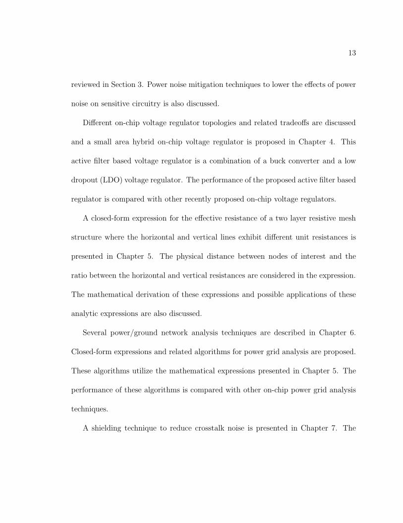
circuits. The power dissipated by microprocessors has grown significantly from 600
mwatts [33] to 100 watts [34], as illustrated in Fig. 2.1 [33–48]. Since the growth in
die area is slower than the increase in power consumption, the power density has also
increased, approaching the power density of a nuclear reactor [22]. With scaling of the
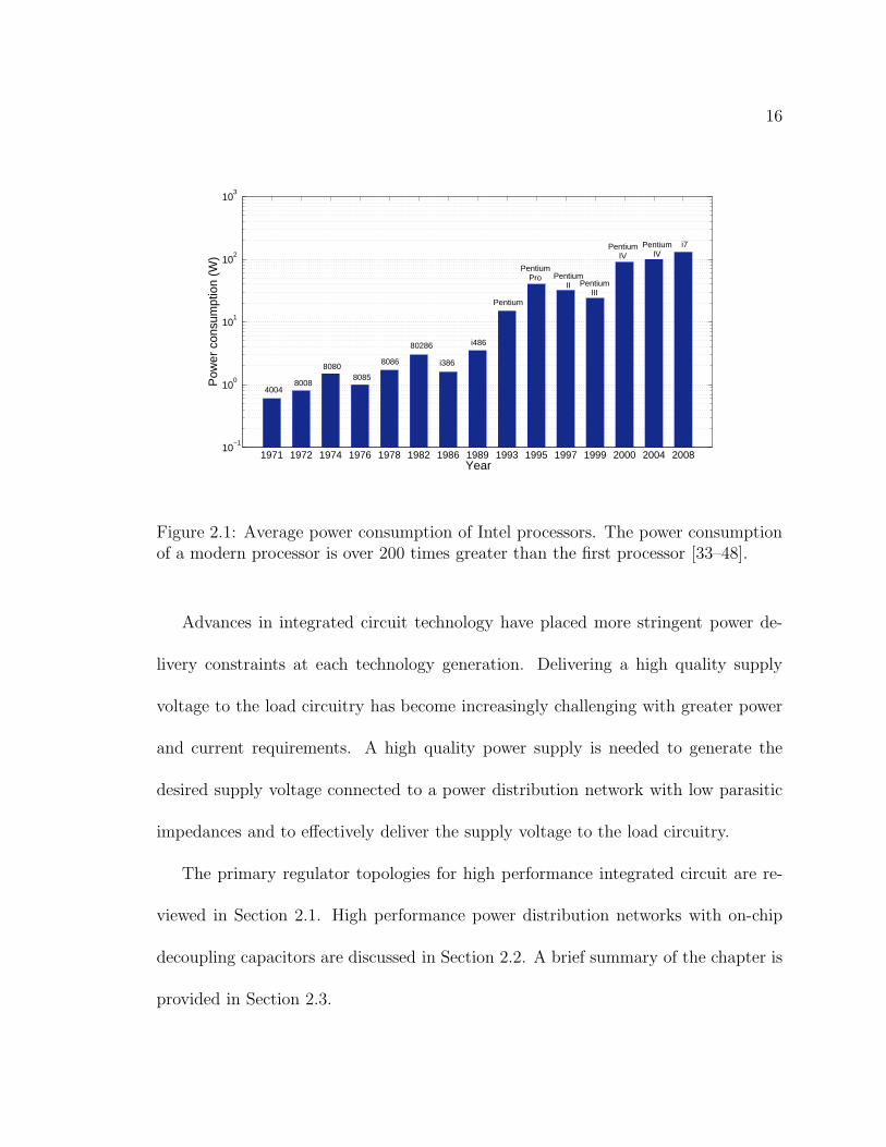
minimum transistor feature size, the voltage supply has also decreased from 15 volts
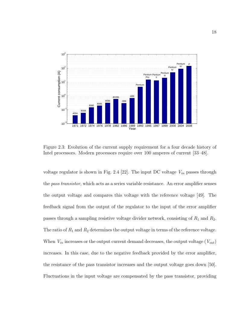
to less than 1 volt, as shown in Fig. 2.2 [33–48]. Furthermore, the current provided to
high performance integrated circuits has increased from 30 mA to over 100 Amps in
modern microprocessors. The evolution of current requirements for microprocessors
is illustrated in Fig. 2.3 [33–48].
16
1971 1972 1974 1976 1978 1982 1986 1989 1993 1995 1997 1999 2000 2004 200810
−1
100
101
102
103
Year
Pow
er c
onsu
mpt
ion
(W)
40048008
80808085
8086 i386
i486
Pentium
PentiumPro Pentium
II PentiumIII
PentiumIV
PentiumIV
i7
80286
Figure 2.1: Average power consumption of Intel processors. The power consumptionof a modern processor is over 200 times greater than the first processor [33–48].
Advances in integrated circuit technology have placed more stringent power de-
livery constraints at each technology generation. Delivering a high quality supply
voltage to the load circuitry has become increasingly challenging with greater power
and current requirements. A high quality power supply is needed to generate the
desired supply voltage connected to a power distribution network with low parasitic
impedances and to effectively deliver the supply voltage to the load circuitry.
The primary regulator topologies for high performance integrated circuit are re-
viewed in Section 2.1. High performance power distribution networks with on-chip
decoupling capacitors are discussed in Section 2.2. A brief summary of the chapter is
provided in Section 2.3.
17
1971 1972 1974 1976 1978 1982 1986 1989 1993 1995 1997 1999 2000 2004 20080
2
4
6
8
10
12
14
Year
Pow
er s
uppl
y (V
)4004
i7
PentiumIV
PentiumIV
PentiumII
i48680868085
8080
8008
80286 i386
PentiumPentium
Pro
PentiumII
Figure 2.2: Evolution of power supply voltages for Intel processors. With advancedCMOS processing technologies, the power supply voltage has shrunk to less than avolt [33–48].
2.1 On-Chip Power Supply Design
Three power supply topologies are reviewed in this section. Linear, switching, and
switched-capacitor voltage supplies are discussed, respectively, in Sections 2.1.1, 2.1.2,
and 2.1.3. A comparison of some of the characteristics of these voltage regulators is
provided in Section 2.1.4.
2.1.1 Linear Voltage Regulators
Linear voltage regulators use the standard form of a voltage regulator with a
simpler feedback structure as compared to other voltage regulators. A basic linear
18
1971 1972 1974 1976 1978 1982 1986 1989 1993 1995 1997 1999 2000 2004 200810
−2
10−1
100
101
102
103
Year
Cur
rent
con
sum
ptio
n (A
)Pentium
IV
PentiumPro
40048008
80808085
8086
80286
i386
i486
Pentium
PentiumII
PentiumIII
PentiumIV
i7
Figure 2.3: Evolution of the current supply requirement for a four decade history ofIntel processors. Modern processors require over 100 amperes of current [33–48].
voltage regulator is shown in Fig. 2.4 [22]. The input DC voltage Vin passes through
the pass transistor, which acts as a series variable resistance. An error amplifier senses
the output voltage and compares this voltage with the reference voltage [49]. The
feedback signal from the output of the regulator to the input of the error amplifier
passes through a sampling resistive voltage divider network, consisting of R1 and R2.
The ratio of R1 and R2 determines the output voltage in terms of the reference voltage.
When Vin increases or the output current demand decreases, the output voltage (Vout)
increases. In this case, due to the negative feedback provided by the error amplifier,
the resistance of the pass transistor increases and the output voltage goes down [50].
Fluctuations in the input voltage are compensated by the pass transistor, providing
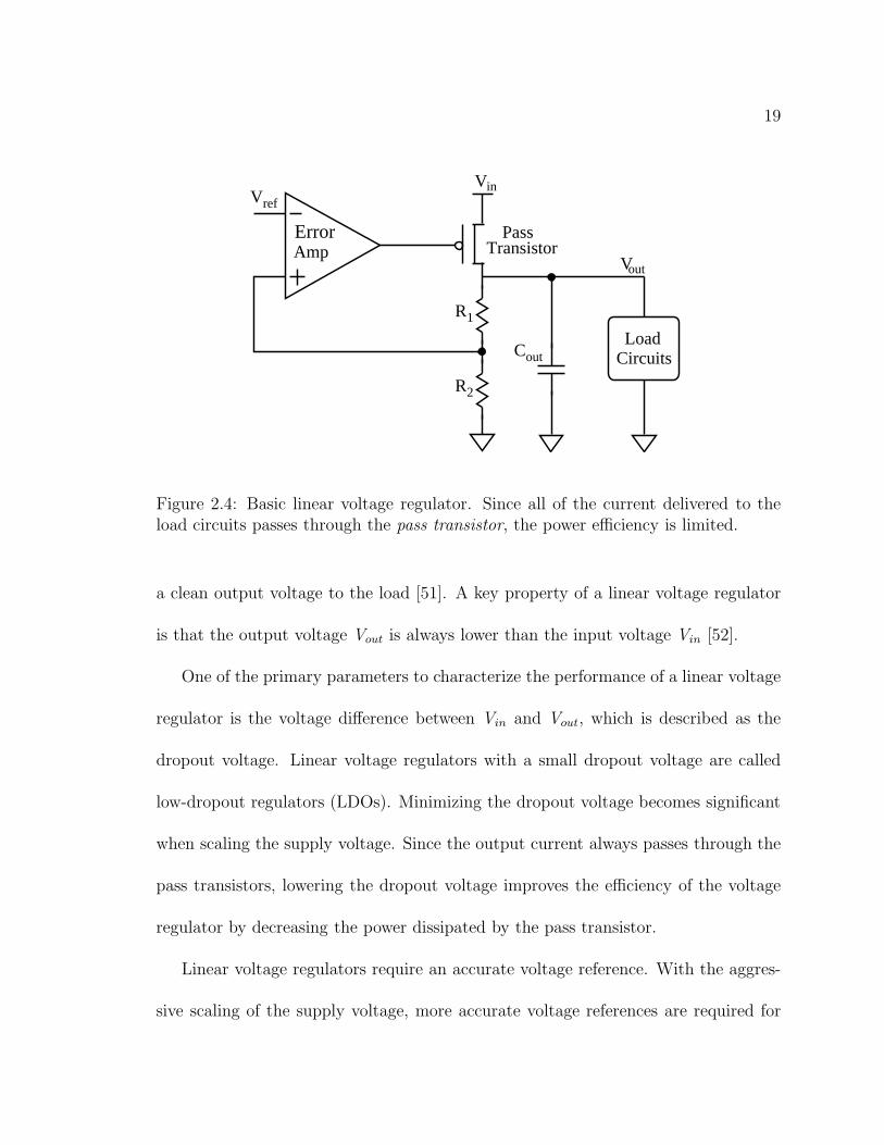
19
R1
R2
Cout
Vref
ErrorAmp
PassTransistor
LoadCircuits
V in
outV
Figure 2.4: Basic linear voltage regulator. Since all of the current delivered to theload circuits passes through the pass transistor, the power efficiency is limited.
a clean output voltage to the load [51]. A key property of a linear voltage regulator
is that the output voltage Vout is always lower than the input voltage Vin [52].
One of the primary parameters to characterize the performance of a linear voltage
regulator is the voltage difference between Vin and Vout, which is described as the
dropout voltage. Linear voltage regulators with a small dropout voltage are called
low-dropout regulators (LDOs). Minimizing the dropout voltage becomes significant
when scaling the supply voltage. Since the output current always passes through the
pass transistors, lowering the dropout voltage improves the efficiency of the voltage
regulator by decreasing the power dissipated by the pass transistor.
Linear voltage regulators require an accurate voltage reference. With the aggres-
sive scaling of the supply voltage, more accurate voltage references are required for
20
linear voltage regulators.
The size of the output capacitor is an issue for on-chip regulators and is there-
fore generally placed off-chip [53–56]. An off-chip output capacitor requires dedicated
I/Os and produces higher parasitic losses. Alternatively, when the output capacitor
is placed on-chip, the output capacitor dominates the total area of the LDO regula-
tor [24]. A high bias current of 6 mA is used in [24] to deliver 100 mA current with
a 600 pF output capacitor. This approach is not appropriate for low power applica-
tions and the output capacitor occupies significant die area. Many techniques have
been proposed to eliminate the need for the large off-chip capacitor without sacrific-
ing the stability and performance of the LDO regulator [24,28,29,57–60]. Adaptively
changing the bias current based on the output current demand is proposed in [56–58].
These techniques, however, do not completely eliminate the need for an output ca-
pacitor. Furthermore, compensation circuitry that produces a dominant pole requires
additional area.
When the load current changes abruptly, voltage spikes occur at the output. The
closed-loop bandwidth of the system and the output capacitor determine the speed
and accuracy of a voltage regulator while regulating transient changes at the out-
put [50]. Load regulation has become an important parameter characterizing voltage
regulators, particularly at higher clock speeds.
21
2.1.2 Switching Voltage Regulators
The power dissipated by the pass transistor within a linear voltage regulator has
motivated the design of more power efficient voltage regulators. Switching voltage
regulators can ideally approach 100% efficiency when the parasitic impedances are
eliminated. Switching converters are therefore the most commonly used type of power
supplies due to the high power efficiency characteristics [22]. There are primarily two
types of switching regulators: 1) a buck converter which is step down and 2) a boost
converter which is step up. A typical buck converter is shown in Fig. 2.5a. In a buck
converter, large tapered buffers drive the power MOSFETs (the PMOS and NMOS
transistors). A switching signal with a finite rise and fall time (respectively, tr and
tf), as shown in Fig. 2.5b, is generated at the output of the power MOSFETs at
node1. The capacitor-inductor (LC) filter removes the high frequency harmonics of
this switching signal from the output voltage. The size of the passive filter determines
the level of suppression of the high frequency harmonics. A larger passive filter would
effectively generate an output voltage with a lower voltage ripple, which is the high
frequency noise component of the generated output voltage due to the non-ideal
nature of the LC filter. The passive inductor and capacitor are generally placed off-
chip due to the significant area requirement [61–65]. To compensate for changes in the
output voltage due to abrupt changes in the load current, a pulse width modulator
(PWM) changes the duty cycle of the switching signal driving the tapered buffers.
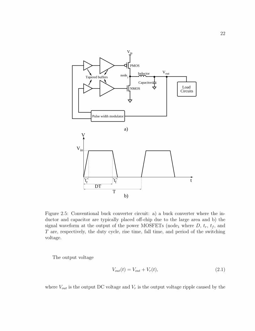
22
Va)
b)
t
TDT
tf
V in
V in
InductorTapered buffers
Capacitor
NMOS
Pulse width modulator
tr
PMOS
node1
Vout
CircuitsLoad
Figure 2.5: Conventional buck converter circuit: a) a buck converter where the in-ductor and capacitor are typically placed off-chip due to the large area and b) thesignal waveform at the output of the power MOSFETs (node1 where D, tr, tf , andT are, respectively, the duty cycle, rise time, fall time, and period of the switchingvoltage.
The output voltage
Vout(t) = Vout + Vr(t), (2.1)
where Vout is the output DC voltage and Vr is the output voltage ripple caused by the
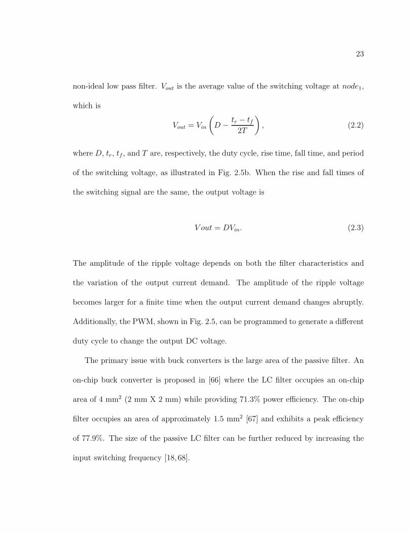
23
non-ideal low pass filter. Vout is the average value of the switching voltage at node1,
which is
Vout = Vin
(
D − tr − tf2T
)
, (2.2)
where D, tr, tf , and T are, respectively, the duty cycle, rise time, fall time, and period
of the switching voltage, as illustrated in Fig. 2.5b. When the rise and fall times of
the switching signal are the same, the output voltage is
V out = DVin. (2.3)
The amplitude of the ripple voltage depends on both the filter characteristics and
the variation of the output current demand. The amplitude of the ripple voltage
becomes larger for a finite time when the output current demand changes abruptly.
Additionally, the PWM, shown in Fig. 2.5, can be programmed to generate a different
duty cycle to change the output DC voltage.
The primary issue with buck converters is the large area of the passive filter. An
on-chip buck converter is proposed in [66] where the LC filter occupies an on-chip
area of 4 mm2 (2 mm X 2 mm) while providing 71.3% power efficiency. The on-chip
filter occupies an area of approximately 1.5 mm2 [67] and exhibits a peak efficiency
of 77.9%. The size of the passive LC filter can be further reduced by increasing the
input switching frequency [18, 68].
24
Magnetic materials on silicon is another approach to move the passive filter com-
ponents on-chip [69]. These techniques are, however, currently not sufficiently cost
effective. A switching frequency of 45 MHz has been achieved with a fully integrated
buck converter (i.e., on-chip capacitor and inductor) with a SiGe RFBiCMOS tech-
nology [70]. Of the several issues in fully monolithic buck converters, most of the
problems relate to the inductor design [71]. Due to the large area requirement, mul-
tiple distributed on-chip power supplies placed close to the load circuitry are not
practical with a buck converter topology.
2.1.3 Switched-Capacitor Voltage Regulators
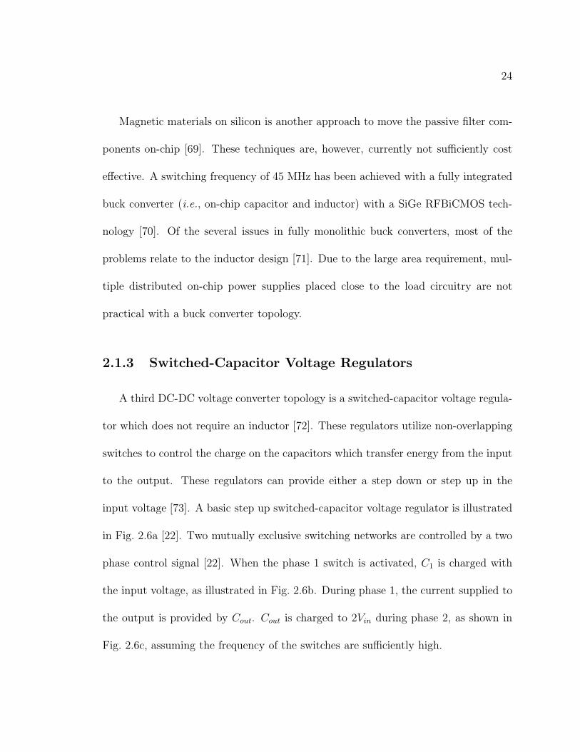
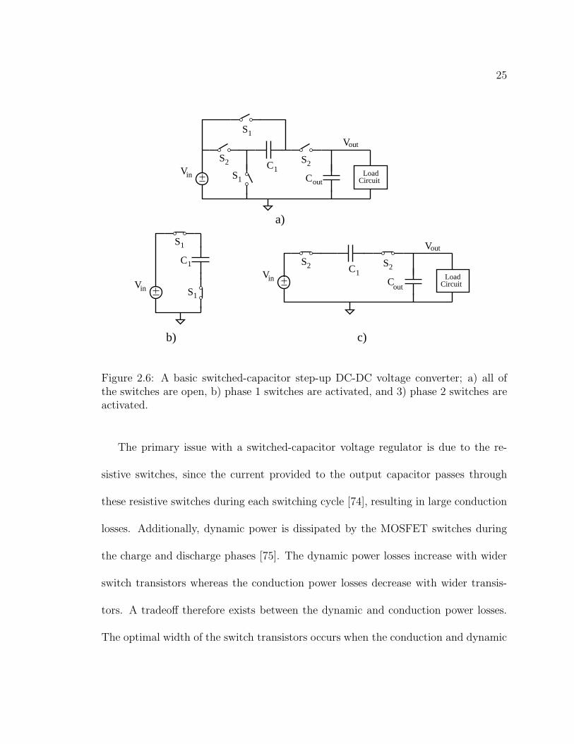
A third DC-DC voltage converter topology is a switched-capacitor voltage regula-
tor which does not require an inductor [72]. These regulators utilize non-overlapping
switches to control the charge on the capacitors which transfer energy from the input
to the output. These regulators can provide either a step down or step up in the
input voltage [73]. A basic step up switched-capacitor voltage regulator is illustrated
in Fig. 2.6a [22]. Two mutually exclusive switching networks are controlled by a two
phase control signal [22]. When the phase 1 switch is activated, C1 is charged with
the input voltage, as illustrated in Fig. 2.6b. During phase 1, the current supplied to
the output is provided by Cout. Cout is charged to 2Vin during phase 2, as shown in
Fig. 2.6c, assuming the frequency of the switches are sufficiently high.
25
outV
outV
Vin
S2S2 C1
CircuitLoad
outCVin
1C
S1
1S
Vin
S2
S1
S1
S2 C1
CircuitLoad
Cout
b) c)
a)
Figure 2.6: A basic switched-capacitor step-up DC-DC voltage converter; a) all ofthe switches are open, b) phase 1 switches are activated, and 3) phase 2 switches areactivated.
The primary issue with a switched-capacitor voltage regulator is due to the re-
sistive switches, since the current provided to the output capacitor passes through
these resistive switches during each switching cycle [74], resulting in large conduction
losses. Additionally, dynamic power is dissipated by the MOSFET switches during
the charge and discharge phases [75]. The dynamic power losses increase with wider
switch transistors whereas the conduction power losses decrease with wider transis-
tors. A tradeoff therefore exists between the dynamic and conduction power losses.
The optimal width of the switch transistors occurs when the conduction and dynamic

26
power losses are equal [75, 76].
A recently proposed switched-capacitor voltage regulator [30] designed in a 45 nm
CMOS technology exhibits over 60% power efficiency while providing less than 10 mA
current and occupies an on-chip area of 0.16 mm2. Another switched-capacitor voltage
regulator proposed in 2010 [31] exhibits a 81% peak power efficiency, although the
converter occupies an on-chip area of 0.36 mm2. Although these switched-capacitor
voltage regulators can provide greater than 80% power efficiency while occupying a
relatively small area as compared to a buck converter, the maximum load current
is limited and cannot compete with an on-chip buck converter. Additionally, these
regulators are not sufficiently small to be integrated as a point-of-load (POL) power
supply to deliver current close to the load circuitry.
2.1.4 A Comparison of Voltage Regulators for On-Chip In-
tegration
Multiple on-chip voltage regulators are needed for modern high performance in-
tegrated circuits [9]. Various parameters should be considered when choosing the
appropriate regulator topology. A table comparing the three types of voltage regu-
lators, which are explained previously in this section, is provided in Table 2.1. The
primary design parameter that affects the development of multiple on-chip power
supplies is the on-chip area. Although linear voltage regulators require smaller area
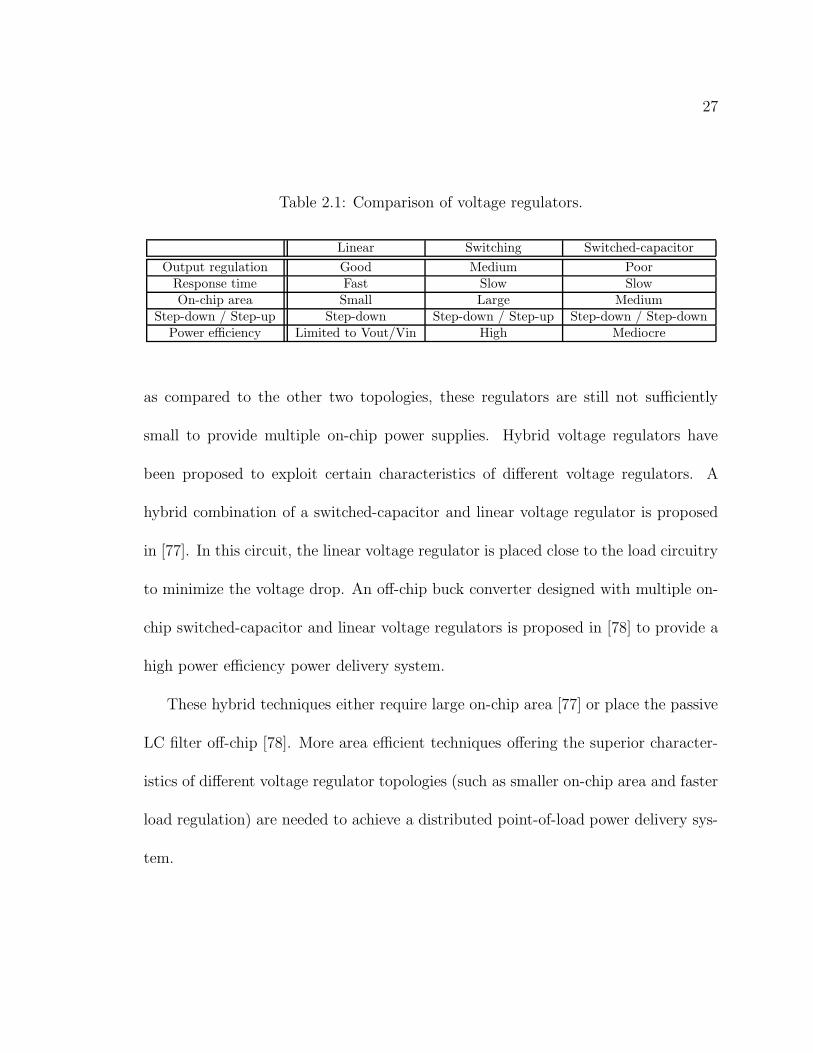
27
Table 2.1: Comparison of voltage regulators.
Linear Switching Switched-capacitor
Output regulation Good Medium PoorResponse time Fast Slow SlowOn-chip area Small Large Medium
Step-down / Step-up Step-down Step-down / Step-up Step-down / Step-downPower efficiency Limited to Vout/Vin High Mediocre
as compared to the other two topologies, these regulators are still not sufficiently
small to provide multiple on-chip power supplies. Hybrid voltage regulators have
been proposed to exploit certain characteristics of different voltage regulators. A
hybrid combination of a switched-capacitor and linear voltage regulator is proposed
in [77]. In this circuit, the linear voltage regulator is placed close to the load circuitry
to minimize the voltage drop. An off-chip buck converter designed with multiple on-
chip switched-capacitor and linear voltage regulators is proposed in [78] to provide a
high power efficiency power delivery system.
These hybrid techniques either require large on-chip area [77] or place the passive
LC filter off-chip [78]. More area efficient techniques offering the superior character-
istics of different voltage regulator topologies (such as smaller on-chip area and faster
load regulation) are needed to achieve a distributed point-of-load power delivery sys-
tem.
28
SupplyPower
c1Lp
c1Rp
p2Lp
p2Rp
c2Lg
c2Rg
cRC
cC
cLC
c1Lg
c1Rg
p2Lg
p2Rg
pRC
pC
pLC
p1Lp
p1Lg
p1Rg
p1Rp
b2Lp
b2Rp
c2Lg
bRC
bC
b1Lg
b1Rg
b1Lp
b1Rp
sLp
sRp
sLg
sRg
c2Rp
c2Lp
b2Rg
bLC
CircuitLoad
Package power networkPrinted circuit board power network On−chip power networkPower supply
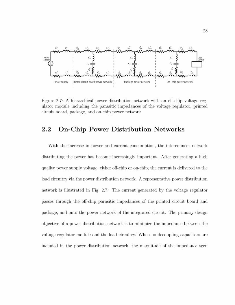
Figure 2.7: A hierarchical power distribution network with an off-chip voltage reg-ulator module including the parasitic impedances of the voltage regulator, printedcircuit board, package, and on-chip power network.
2.2 On-Chip Power Distribution Networks
With the increase in power and current consumption, the interconnect network
distributing the power has become increasingly important. After generating a high
quality power supply voltage, either off-chip or on-chip, the current is delivered to the
load circuitry via the power distribution network. A representative power distribution
network is illustrated in Fig. 2.7. The current generated by the voltage regulator
passes through the off-chip parasitic impedances of the printed circuit board and
package, and onto the power network of the integrated circuit. The primary design
objective of a power distribution network is to minimize the impedance between the
voltage regulator module and the load circuitry. When no decoupling capacitors are
included in the power distribution network, the magnitude of the impedance seen

29
from the load circuit is
|Ztotal(w)| = |Rtotal + jwLtotal|. (2.4)
Note in (2.4) that the impedance of the power distribution network increases with
frequency. To maintain the impedance seen from the load circuitry below a maximum
target impedance Ztarget under a high load current demand, intentional decoupling
capacitors, Cb, Cp, and Cc, are placed hierarchically on the board, package, and
on-chip power distribution networks, respectively, as illustrated in Fig. 2.7.
A general overview of decoupling capacitors is presented in Section 2.2.1. High
performance on-chip power distribution networks are discussed in Section 2.2.4
2.2.1 Decoupling Capacitors
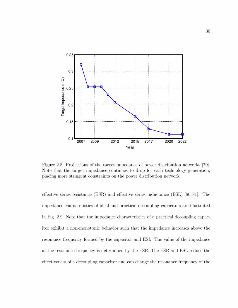
With the higher current demand of the load circuits and faster transition times
of the signal waveforms, the maximum target impedance has decreased at an aggres-
sive rate for each technology generation [79], as illustrated in Fig. 2.8. To maintain
stringent noise constraints for higher quality power supply delivery, the impedance
between the power supply and load circuitry is reduced by placing decoupling ca-
pacitors throughout the power distribution network. Decoupling capacitors operate
as a local reservoir of charge, providing charge to the load circuitry during transient
changes in the load current [13]. The decoupling capacitors, however, have a parasitic
30
Figure 2.8: Projections of the target impedance of power distribution networks [79].Note that the target impedance continues to drop for each technology generation,placing more stringent constraints on the power distribution network.
effective series resistance (ESR) and effective series inductance (ESL) [80, 81]. The
impedance characteristics of ideal and practical decoupling capacitors are illustrated
in Fig. 2.9. Note that the impedance characteristics of a practical decoupling capac-
itor exhibit a non-monotonic behavior such that the impedance increases above the
resonance frequency formed by the capacitor and ESL. The value of the impedance
at the resonance frequency is determined by the ESR. The ESR and ESL reduce the
effectiveness of a decoupling capacitor and can change the resonance frequency of the
31
Frequency (log)
Impe
danc
e (lo
g)
−20 dB/dec
−20 dB/dec 20 d
B/dec
Frequency (log)Im
peda
nce
(log)
w res
ES
R
capacitive induc
tive
CESRESL
C
Practical decoupling capacitorIdeal decoupling capacitor
Figure 2.9: Ideal and practical decoupling capacitors. Although the impedance ofan ideal decoupling capacitor decreases linearly, the impedance of a practical decou-pling capacitance does not decrease monotonically, causing a constant increase in theimpedance above the resonance frequency due to the ESL of the capacitor.
power distribution network [13,82,83]. When two capacitors are connected in parallel,
antiresonance occurs. At this antiresonance frequency, the impedance of the system
significantly increases, producing a peak impedance [13].
Hierarchical power distribution networks with board, package, and on-chip decou-
pling capacitors are explained in Section 2.2.2. Different technologies to implement
on-chip decoupling capacitors are reviewed in Section 2.2.3.
32
CpCb
Cc
Ztarget
f0Frequency, log
Impe
danc
e, lo
g
Figure 2.10: Impedance characteristics of a hierarchical power distribution networkwith board, package, and on-chip decoupling capacitors. The impedance is main-tained below the target impedance Ztarget over a wide frequency range below theoperating frequency of the integrated circuit. The impedance characteristics of eachindividual decoupling capacitor are illustrated by the thin solid lines.
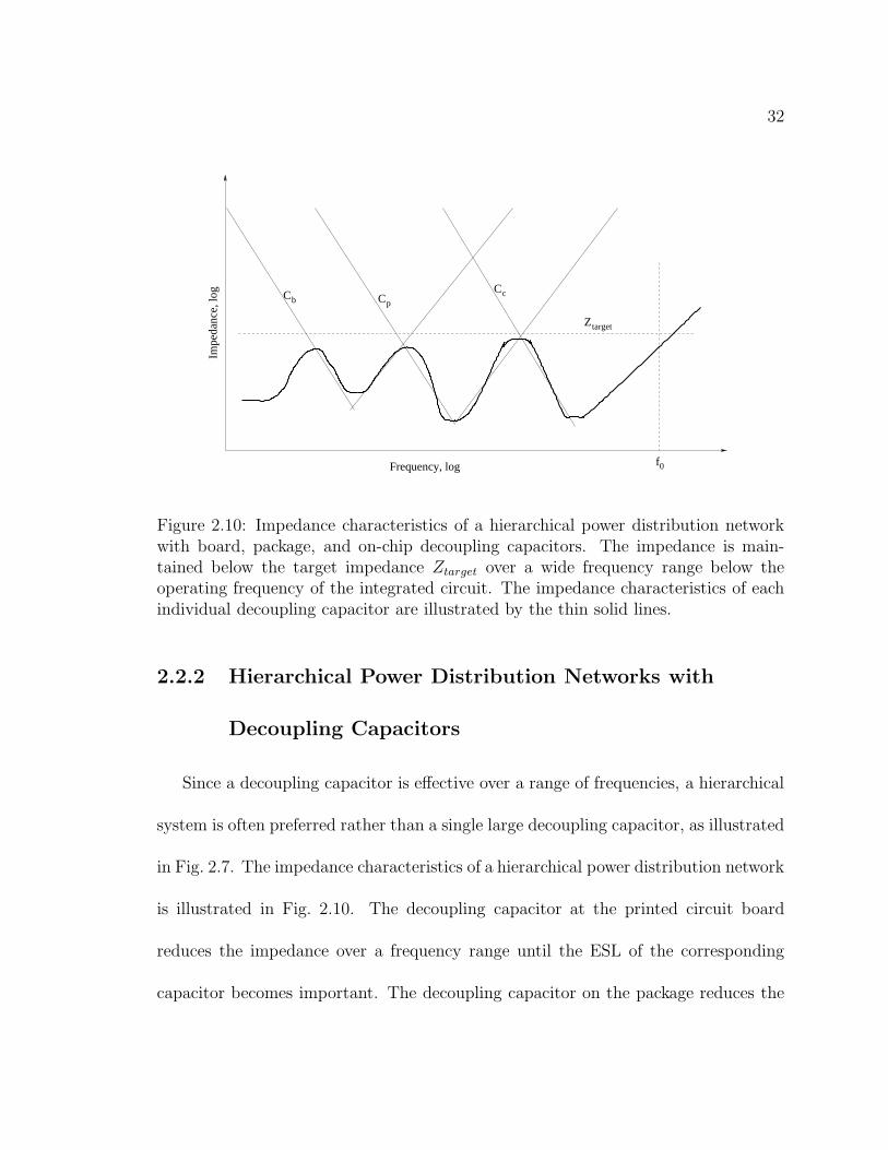
2.2.2 Hierarchical Power Distribution Networks with
Decoupling Capacitors
Since a decoupling capacitor is effective over a range of frequencies, a hierarchical
system is often preferred rather than a single large decoupling capacitor, as illustrated
in Fig. 2.7. The impedance characteristics of a hierarchical power distribution network
is illustrated in Fig. 2.10. The decoupling capacitor at the printed circuit board
reduces the impedance over a frequency range until the ESL of the corresponding
capacitor becomes important. The decoupling capacitor on the package reduces the
33
impedance until the ESL again becomes important. Lastly, the on-chip decoupling
capacitor reduces the impedance for a higher frequency range until the ESL once
again takes effect. The impedance of a power distribution network can therefore
be maintained below a target impedance Ztarget over the frequency range of interest
below the maximum operating frequency of the integrated circuit, as shown as f0 in
Fig. 2.10.
In addition to the intentional decoupling capacitors discussed in this section, in-
trinsic decoupling capacitors provide a native parasitic capacitance between the power
and ground terminals [84]. Certain capacitance mechanisms contribute to the intrin-
sic decoupling capacitance [85]; 1) the intrinsic capacitance of the interconnect lines,
2) the parasitic device capacitances such as the drain junction and gate-to-source ca-
pacitances, and 3) the p-n junction capacitance of the diffusion wells. To accurately
determine the amount of intrinsic decoupling capacitance is a highly challenging prob-
lem. For example, the input vectors to the integrated circuit and the interconnect
network connections should be known a priori to accurately determine the effective
intrinsic decoupling capacitance [86]. The overall intrinsic decoupling capacitance can
be described as
Cintrinsic = Cint + Cpn + Cwell + Cload + Cgs + Cgb, (2.5)
where Cint is the interconnect capacitance, Cpn is the p-n junction capacitance, Cwell

34
is the well capacitance, Cload is the load capacitance, Cgs is the gate-to-source capac-
itance, and Cgb is the gate-to-body capacitance.
2.2.3 On-Chip Decoupling Capacitors
Multiple on-chip decoupling capacitors are used in modern integrated circuits [87–
90] to maintain power integrity. Different techniques are used to design an on-chip
decoupling capacitor.
Polysilicon-insulator-polysilicon (PIP) capacitors utilize two polysilicon electrodes
with either an oxide or oxide-nitride-oxide dielectric [91, 92]. Since the capacitor
dielectric material is unique to this technique, an additional process step is required
for a PIP capacitor in a CMOS process. PIP capacitors also exhibit a low capacitance
density, an undesirable property for on-chip decoupling capacitors.
Metal-insulator-metal (MIM) capacitors use two metal planes separated by a di-
electric layer [93,94]. A thick oxide layer is generally deposited onto the substrate to
reduce the parasitic capacitance to the substrate [13]. MIM capacitors exhibit high
linearity, low process and temperature variations, and low leakage [95,96]. The capac-
itance density, however, is limited since conventional MIM capacitors utilize SiO2 as
the deposited dielectric between the metal layers. Despite these excellent properties,
conventional MIM capacitors are not appropriate as decoupling capacitors due to the
low capacitance density [13]. Different dielectric materials such as Al2O3, AlTiOx [97],
35
AlTaOx [98], HfO2 [93,99], and Pr2O3 [100] are utilized to provide a high density MIM
capacitor. A high density MIM capacitor based on stacked TiO2 and ZrO2 insulators
achieves a capacitance density of 38 fF/µm2 [101]. With stacked metal layers, a high
capacitance density can be achieved. A capacitance density of 440 fF/µm2 [102] is
achieved with a triple layer stacked capacitor in 3-D silicon technology. With in-
creased capacitance densities, MIM capacitors have become the best candidate for
on-chip decoupling capacitors [13]. These new dielectric materials, however, need to
be integrated into the process technology which increases production costs.
MOS capacitors are the most widely used decoupling capacitor technique due
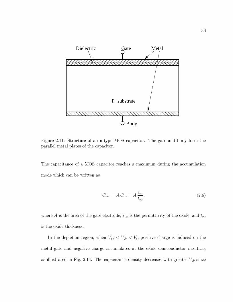
to the simple structure based on existing process steps [103, 104]. The gate of the
MOSFET transistor forms one of the plates of the capacitor. The bulk contact of the
transistor forms the lower parallel plate of the capacitor, as illustrated in Fig. 2.11.
The capacitance density of a MOS capacitor depends upon the voltage difference
between the gate and body terminals. Three regions of operation, accumulation,
depletion, and inversion, can be distinguished from Fig. 2.12. These three regions of
operation are approximately separated by the threshold voltage (Vt) and flat band
voltage (Vfb). Vfb can be defined as the voltage when no charge accumulation occurs
on the plates of the capacitor (i.e., no electric field across the dielectric) [13].
In the accumulation region, when Vgb < Vfb, the negative charge is accumulated
on the metal gate and positive charge in the semiconductor, as illustrated in Fig. 2.13.
36
Dielectric MetalGate
Body
P−substrate
Figure 2.11: Structure of an n-type MOS capacitor. The gate and body form theparallel metal plates of the capacitor.
The capacitance of a MOS capacitor reaches a maximum during the accumulation
mode which can be written as
Cacc = ACox = Aǫoxtox
, (2.6)
where A is the area of the gate electrode, ǫox is the permittivity of the oxide, and tox
is the oxide thickness.
In the depletion region, when Vfb < Vgb < Vt, positive charge is induced on the
metal gate and negative charge accumulates at the oxide-semiconductor interface,
as illustrated in Fig. 2.14. The capacitance density decreases with greater Vgb since
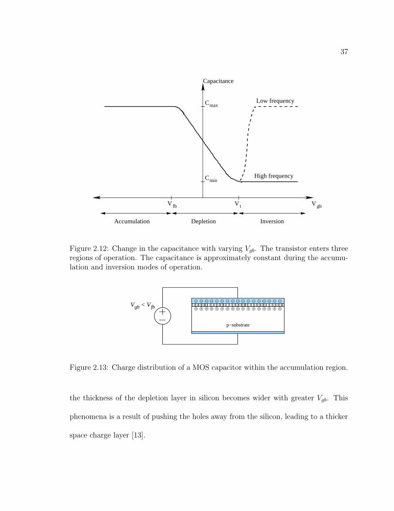
37
Cmin
CmaxLow frequency
High frequency
Capacitance
V gbV tV fb
Depletion InversionAccumulation
Figure 2.12: Change in the capacitance with varying Vgb. The transistor enters threeregions of operation. The capacitance is approximately constant during the accumu-lation and inversion modes of operation.
Vgb < V
fb
p−substrate
Figure 2.13: Charge distribution of a MOS capacitor within the accumulation region.
the thickness of the depletion layer in silicon becomes wider with greater Vgb. This
phenomena is a result of pushing the holes away from the silicon, leading to a thicker
space charge layer [13].
38
xd
p−substrate
Vfb < Vgb < Vt
Figure 2.14: Charge distribution of a MOS capacitor within the depletion region.
dxVt < Vgb
p−substrate
Figure 2.15: Charge distribution of a MOS capacitor within the inversion region.
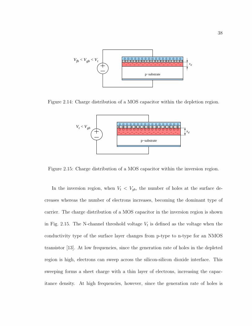
In the inversion region, when Vt < Vgb, the number of holes at the surface de-
creases whereas the number of electrons increases, becoming the dominant type of
carrier. The charge distribution of a MOS capacitor in the inversion region is shown
in Fig. 2.15. The N-channel threshold voltage Vt is defined as the voltage when the
conductivity type of the surface layer changes from p-type to n-type for an NMOS
transistor [13]. At low frequencies, since the generation rate of holes in the depleted
region is high, electrons can sweep across the silicon-silicon dioxide interface. This
sweeping forms a sheet charge with a thin layer of electrons, increasing the capac-
itance density. At high frequencies, however, since the generation rate of holes is
39
not sufficiently high, a sheet charge with a thin layer of electrons cannot be formed.
The thickness of the silicon depletion layer therefore reaches the maximum at high
frequencies, reducing the capacitance density, as illustrated in Fig. 2.12.
MOS capacitors are typically preferred for decoupling capacitors due to the high
capacitance density and natural compatibility with existing CMOS technologies [104].
The leakage current is the primary issue for MOS capacitors. The leakage current
of a MOS capacitor further increases with technology scaling, increasing the overall
power dissipation [105,106]. To reduce leakage current in MOS capacitors, the capac-
itors should operate in the accumulation region since a 15 times reduction in leakage
current can be achieved with MOS capacitors operating in the accumulation region
as compared to MOS capacitors operating in the depletion region [107].
2.2.4 On-Chip Power Distribution Networks
The structure and impedance characteristics of a hierarchical power distribution
network with decoupling capacitors are discussed in the previous section. A one-
dimensional structure is not a practical model of an on-chip power distribution net-
work for high performance design and analysis. On-chip power distribution networks
exhibit a non-uniform structure since the current consumption of different blocks
varies throughout the die [108]. The on-chip power distribution network should there-
fore be considered as a two- or three-dimensional structure [13, 109–112].

40
Different power distribution network topologies commonly used in modern in-
tegrated circuits are discussed in Section 2.2.42.2.4.1 The die-package interface is
reviewed in Section 2.2.42.2.4.2
2.2.4.1 Topologies of Power Distribution Networks
Different topologies are used to design on-chip power distribution networks. The
primary constraints when choosing an appropriate topology are the available metal re-
sources to route the power/ground signals, the noise constraints on the load circuitry,
and the area constraints of the integrated circuit.
Different circuit blocks are connected with wide interconnect lines in routed power
distribution networks. Each circuit block has a local power distribution network to
satisfy the noise constraints of the load circuitry. A representative integrated circuit
with a routed power/ground network is illustrated in Fig. 2.16a. The low redundancy
of routed power distribution networks is the primary problem since most of the current
delivered to a circuit block is provided by one or two power lines [13].
A mesh structured power/ground distribution network is used when the reliability
and noise constraints are satisfied with limited interconnect resources, often in low
power applications [113]. A mesh power/ground network is illustrated in Fig. 2.16b.
The horizontal power/ground lines are connected with short wires from the lower
metal layers. Mesh power/ground networks are also utilized to distribute power and
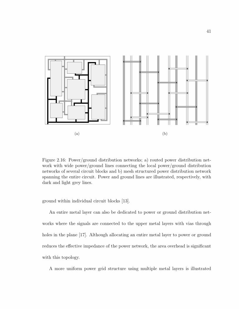
41
(a) (b)
Figure 2.16: Power/ground distribution networks; a) routed power distribution net-work with wide power/ground lines connecting the local power/ground distributionnetworks of several circuit blocks and b) mesh structured power distribution networkspanning the entire circuit. Power and ground lines are illustrated, respectively, withdark and light grey lines.
ground within individual circuit blocks [13].
An entire metal layer can also be dedicated to power or ground distribution net-
works where the signals are connected to the upper metal layers with vias through
holes in the plane [17]. Although allocating an entire metal layer to power or ground
reduces the effective impedance of the power network, the area overhead is significant
with this topology.
A more uniform power grid structure using multiple metal layers is illustrated
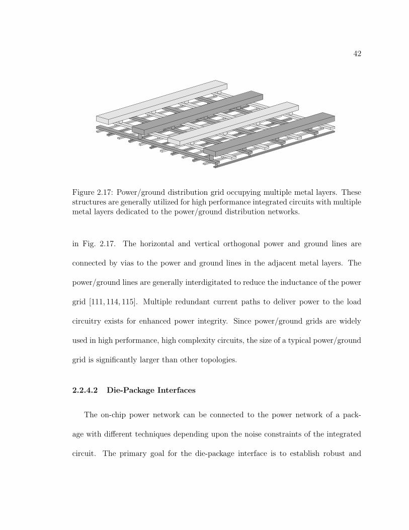
42
Figure 2.17: Power/ground distribution grid occupying multiple metal layers. Thesestructures are generally utilized for high performance integrated circuits with multiplemetal layers dedicated to the power/ground distribution networks.
in Fig. 2.17. The horizontal and vertical orthogonal power and ground lines are
connected by vias to the power and ground lines in the adjacent metal layers. The
power/ground lines are generally interdigitated to reduce the inductance of the power
grid [111, 114, 115]. Multiple redundant current paths to deliver power to the load
circuitry exists for enhanced power integrity. Since power/ground grids are widely
used in high performance, high complexity circuits, the size of a typical power/ground
grid is significantly larger than other topologies.
2.2.4.2 Die-Package Interfaces
The on-chip power network can be connected to the power network of a pack-
age with different techniques depending upon the noise constraints of the integrated
circuit. The primary goal for the die-package interface is to establish robust and
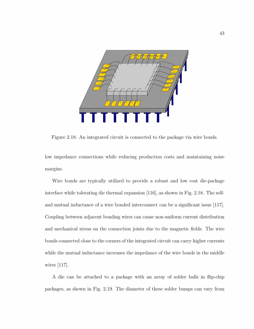
43
Figure 2.18: An integrated circuit is connected to the package via wire bonds.
low impedance connections while reducing production costs and maintaining noise
margins.
Wire bonds are typically utilized to provide a robust and low cost die-package
interface while tolerating die thermal expansion [116], as shown in Fig. 2.18. The self-
and mutual inductance of a wire bonded interconnect can be a significant issue [117].
Coupling between adjacent bonding wires can cause non-uniform current distribution
and mechanical stress on the connection joints due to the magnetic fields. The wire
bonds connected close to the corners of the integrated circuit can carry higher currents
while the mutual inductance increases the impedance of the wire bonds in the middle
wires [117].
A die can be attached to a package with an array of solder balls in flip-chip
packages, as shown in Fig. 2.19. The diameter of these solder bumps can vary from

44
25 µm to 150 µm [118]. Flip-chip packages provide a more robust interface between
the package and die as compared to wire bonded connections. The number of I/O
connections has significantly increased with flip-chip packaging because the number
of I/O connections does not depend on the perimeter of the integrated circuit as
with wire bonded connections. A high quality supply voltage is delivered to the load
circuitry due to the reduced interconnect parasitic impedances. The inductance of a
solder ball connection typically ranges from 0.1 nH to 0.5 nH which is significantly
smaller than the inductance of a wire bond. The reduced parasitic inductance and
shorter distance between the supply connection and the load circuitry improves the
noise characteristics of the integrated circuit. Decoupling capacitors can be placed on
the underside of the package, thereby reducing the parasitic impedances between the
decoupling capacitors and the voltage supply [119]. Testing integrated circuits with
flip chip connections, however, is more difficult as compared to wire bonded circuits.
Lead-free solders are attracting more attention [120, 121] due to environmental
regulations. Lead-free solders have now become a requirement in Europe after the
Restriction of Hazardous Substances Directive (RoHS) was adapted in February 2003
by the European Union [122]. Additional environmental standards are now required
by other countries or companies.
A completely solderless package is being investigated since most of the yield loss
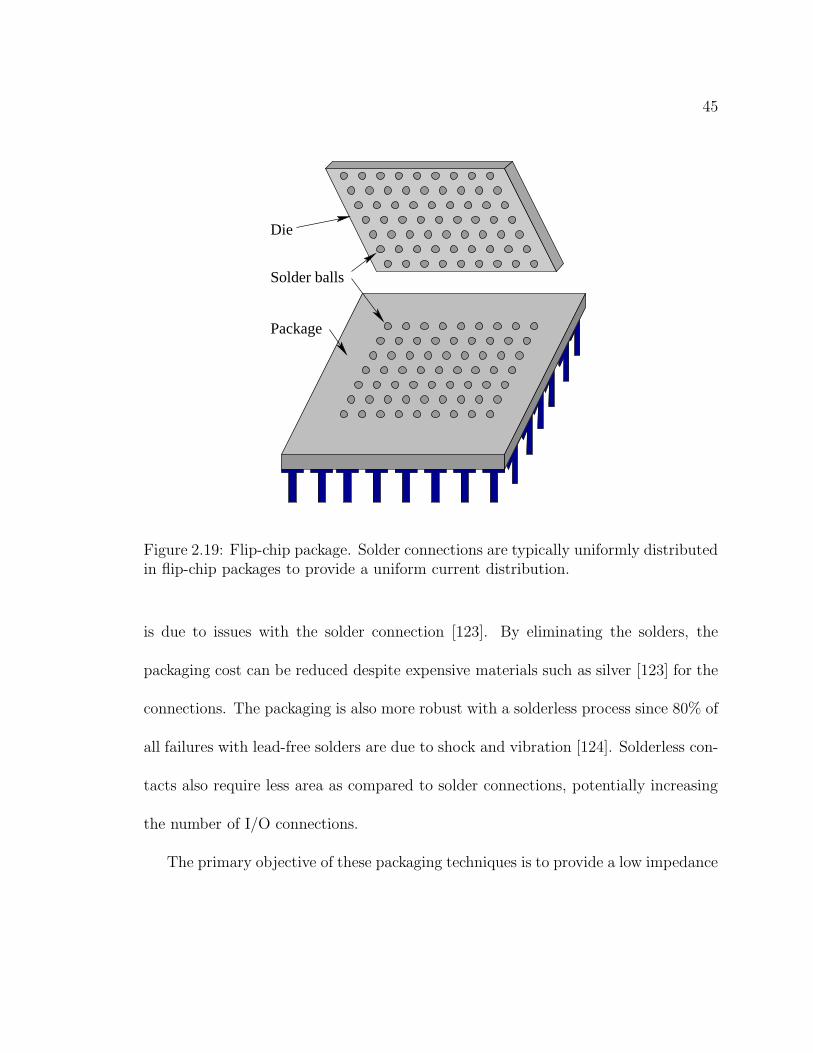
45
Die
Package
Solder balls
Figure 2.19: Flip-chip package. Solder connections are typically uniformly distributedin flip-chip packages to provide a uniform current distribution.
is due to issues with the solder connection [123]. By eliminating the solders, the
packaging cost can be reduced despite expensive materials such as silver [123] for the
connections. The packaging is also more robust with a solderless process since 80% of
all failures with lead-free solders are due to shock and vibration [124]. Solderless con-
tacts also require less area as compared to solder connections, potentially increasing
the number of I/O connections.
The primary objective of these packaging techniques is to provide a low impedance
46
path between the power supply, decoupling capacitor, and load circuitry while im-
proving reliability and reducing cost. With the increased functionality and high cur-
rent consumption of high performance integrated circuits, delivering a high quality
supply voltage to the active circuitry is a highly challenging task. Novel techniques
are required to reduce the effective impedance between the power supplies and the
load circuitry. These techniques span a variety of disciplines such as packaging and
semiconductor process technologies, circuit design techniques, and algorithms and
methodologies to optimally allocate the available resources to improve power and
signal integrity.
2.3 Summary
A variety of power generation and distribution techniques for high performance
integrated circuits are reviewed in this chapter. Different power supply topologies,
such as linear, switched-capacitor, and switching voltage regulators, are described.
The advantages and disadvantages of these power supplies are compared for various
design parameters such as power efficiency, on-chip area, and load regulation.
The effect of hierarchical decoupling capacitors on the impedance characteristics
of the board, package, and on-chip power distribution networks is discussed. The
parasitic impedances of the decoupling capacitors are reviewed. Different on-chip
capacitor techniques such as MIM, MOS, and PIP are described and related tradeoffs

47
are explained.
On-chip power distribution topologies, such as routed, mesh structured, and grid
structured, are discussed and related tradeoffs that satisfy design constraints are
reviewed. Routed and mesh structured power distribution networks are typically uti-
lized when the metal resources are limited and the noise constraints are not particu-
larly tight. Grid structured power distribution networks are used in high performance
integrated circuits with tight noise constraints and multiple metal layers dedicated
to the power/ground distribution network. The die/package interface techniques are
also reviewed.

48
Chapter 3
Power Noise Analysis
With the continuous increase in power consumption and decrease in supply volt-
age, as shown in Figs 2.1 and 2.2, voltage fluctuations within the power distribution
network have become significant. Furthermore, the size of a power distribution net-
work increases with the complexity of the circuit although the minimum feature size
continues to decrease. The deleterious effects of power/ground noise should be con-
sidered when designing the noise sensitive circuit blocks. Noise propagated within the
power grid can couple to these noise sensitive circuit blocks. Techniques to mitigate
the propagation and coupling of this detrimental power/ground noise to the noise
sensitive circuits are an important research topic as noise margins are reduced. The
power distribution network of a modern microprocessor typically contains more than
ten million nodes. Analysis of this large and complex system is therefore highly time
consuming, if feasible. Several power grid analysis techniques have been proposed to
accelerate the analysis process.

49
Power network modeling and an overview of different power grid analysis tech-
niques are reviewed in Section 3.1. A brief summary of the chapter is provided in
Section 3.2.
3.1 Power Network Modeling and Analysis
Power distribution modeling is explained in Section 3.1.1. Different power grid
analysis techniques are reviewed in Section 3.1.2.
3.1.1 Models of Power Distribution Networks
A power distribution network consists of interconnect wires exhibiting resistive,
inductive, and capacitive parasitic impedances, power sources such as on-chip power
supplies, I/O power pads or C4 bumps, power loads such as logic circuits, transistors,
buffers and latches, and intentional decoupling capacitors [13]. To analyze a power
distribution network, all of these components should be modeled with sufficient ac-
curacy. There is, however, a tradeoff between the accuracy of the models and the
computational speed of the analysis. Additionally, accurate models are not typically
available during the early design analysis phase when the location of the power con-
nections, wire widths and pitches, and routing of the power and ground lines are not
yet known. Albeit, difficulties in determining a sufficiently accurate model during the
early power grid analysis process is quite important [125].

50
Figure 3.1: Power grid model consisting of power sources, current loads, and decou-pling capacitors.
The power grid consists of interconnect wires delivering current from the power
sources to the power loads through multiple metal layers connected with metal vias.
This interconnection network is typically connected to the power sources at the top
metal layer and to the power loads at the bottom metal layer. The interconnect par-
asitic impedances within a power grid are typically modeled as time-invariant passive
components [126]. The number of these components can easily exceed hundreds of
millions in power grids within modern processors. A schematic model of a power grid
with power sources and drains is shown in Fig. 3.1
The current loads within a power grid exhibit highly nonlinear behavior due to
the nature of the logical components receiving the currents. A piecewise linear circuit
model is typically used in transient analysis to incorporate the effects of this nonlinear
behavior. For instance, the current profile of a circuit block is typically modeled as a
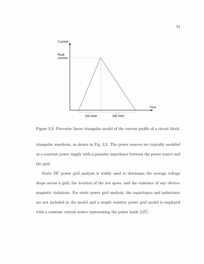
51
Time
rise time fall time
Peakcurrent
Current
Figure 3.2: Piecewise linear triangular model of the current profile of a circuit block.
triangular waveform, as shown in Fig. 3.2. The power sources are typically modeled
as a constant power supply with a parasitic impedance between the power source and
the grid.
Static DC power grid analysis is widely used to determine the average voltage
drops across a grid, the location of the hot spots, and the existence of any electro-
magnetic violations. For static power grid analysis, the capacitance and inductance
are not included in the model and a simple resistive power grid model is employed
with a constant current source representing the power loads [127].
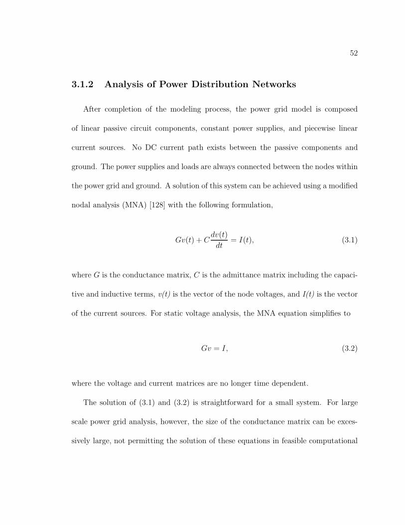
52
3.1.2 Analysis of Power Distribution Networks
After completion of the modeling process, the power grid model is composed
of linear passive circuit components, constant power supplies, and piecewise linear
current sources. No DC current path exists between the passive components and
ground. The power supplies and loads are always connected between the nodes within
the power grid and ground. A solution of this system can be achieved using a modified
nodal analysis (MNA) [128] with the following formulation,
Gv(t) + Cdv(t)
dt= I(t), (3.1)
where G is the conductance matrix, C is the admittance matrix including the capaci-
tive and inductive terms, v(t) is the vector of the node voltages, and I(t) is the vector
of the current sources. For static voltage analysis, the MNA equation simplifies to
Gv = I, (3.2)
where the voltage and current matrices are no longer time dependent.
The solution of (3.1) and (3.2) is straightforward for a small system. For large
scale power grid analysis, however, the size of the conductance matrix can be exces-
sively large, not permitting the solution of these equations in feasible computational

53
time. Advanced techniques are therefore utilized to produce a solution to this sys-
tem of equations. These techniques can be categorized as direct solvers and iterative
techniques. Direct solvers include SPICE, complete Cholesky decomposition, LU fac-
torization, and Gaussian elimination and are deterministic and robust with minimal
convergence issues. For large problems, however, direct solvers are slow as compared
to iterative techniques. Another primary issue with direct solvers is the huge memory
required to store the matrix components.
Iterative techniques include Gauss-Seidel, conjugate gradients, generalized mini-
mal residual (GMRES), and successive over relaxation methods. A sequence of vectors
is constructed after each iteration which can converge to a final result. The system
matrix G is symmetric, positive definitive, and highly sparse. For a resistive network,
however, G can be ill conditioned [125]. This ill condition may produce convergence
issues if iterative methods are used. Iterative techniques may require a precondi-
tioner to ensure fast convergence and efficient computational speed. Among iterative
techniques, Cholesky factorization is well suited for power grid analysis since the con-
ductance matrix is symmetric positive definitive and sparse [125]. Power grid analysis
techniques such as Jacobi, Gauss-Seidel, and successive over relaxation exploit either
the sparsity of the conductance matrix or the special properties of power grids such
as spatial locality and symmetry.

54
In the remainder of this section, several power grid analysis techniques are re-
viewed. In Section 3.1.2.1, stationary and nonstationary iterative techniques are
reviewed. These techniques typically exploit the sparse nature of the conductance
matrix to speed up the analysis process. Power grid analysis techniques which ex-
ploit the distinctive physical properties of a power grid are reviewed in the remaining
sections. In Section 3.1.2.2, hierarchical power grid analysis techniques are reviewed
where the circuit blocks are represented as macromodels to partition the power grid.
A multigrid approach is discussed in Section 3.1.2.3 where the smoothness of the
voltage differences within a power grid is exploited. A random walk based method
is reviewed in Section 3.1.2.4 where the power grid is modeled as a undirected graph
and the graph-based random walk method is described.
3.1.2.1 Iterative Techniques
Iterative techniques can be categorized as stationary and nonstationary iterative
methods. The computations for each iteration are the same for stationary methods
whereas the computations at each iteration changes dynamically in nonstationary
methods depending upon the previous computations. Primary stationary methods
are Jacobi, Gauss-Seidel, and successive over-relaxation methods.
Different iterative methods used for power grid analysis exploit the sparsity of
the system matrices. For the Jacobi method, each diagonal element in a matrix

55
is solved at each iteration. Convergence of this method is quite slow [129]. The
Jacobi method becomes the Gauss-Seidel method if the matrix entries are examined
one at a time and the results of these computations are immediately updated in the
solution matrix before each iteration. The Gauss-Seidel method can be used when the
diagonal entries of the matrix are non-zero. Convergence is guaranteed if the matrix
is symmetric positive definitive. The Gauss-Seidel method converges faster than the
Jacobi method since the computed entries are immediately updated in the following
iteration. Successive over-relaxation is an extrapolation of the Gauss-Seidel method
where the last two computed entries (rather than the last computed entry) are used
in the next iteration.
Modified Gauss-Seidel and successive over-relaxation methods are applied in [130].
A node-based method is proposed in [130] where a node voltage is iteratively deter-
mined with respect to the neighboring node voltages using Kirchoff’s current law. A
row-based method is also proposed where all of the node voltages in a row is based
on the node voltage in the adjacent rows. These two techniques are equivalent to the
Gauss-Seidel method. Improved node- and row-based versions of these techniques use
the final two computed voltages, similar to the successive over-relaxation method.
From a large number of nonstationary iterative methods, the conjugate gradient
method is the preferred option for power grid analysis. A sequence of orthogonal

56
vectors are generated during the conjugate gradient method. These orthogonal vec-
tors are residuals of the approximations to the exact solution, where the algorithm
attempts to minimize these residuals. This technique is highly effective in solving
symmetric positive definite matrices and is therefore widely used in power grid anal-
ysis since only a limited number of matrices are stored within the memory. In [125],
a conjugate gradient iterative scheme with incomplete Cholesky preconditioning1 is
applied to analyze power grids.
3.1.2.2 Hierarchical Power Grid Analysis
A power distribution network can consist of millions of nodes. The computational
power and memory resources are often unable to perform a voltage drop analysis
in feasible time. The power distribution network, however, has distinct properties
which can be exploited to significantly speed up the analysis process. One of these
techniques to analyze the power grid is hierarchy, where macromodels are generated
for local partitions. These macromodels are connected to a global grid with port
admittance matrices, as illustrated in Fig. 3.3. With hierarchical methods, the size
of the power grid analysis problem can be reduced while maintaining the sparsity of
the system matrices [131]. Maintaining sparsity of the local macromodels and port
admittance matrices is, however, not straightforward although the initial conductance
1An incomplete Cholesky decomposition of a matrix M is the sparse approximation of theCholesky factorization on M .
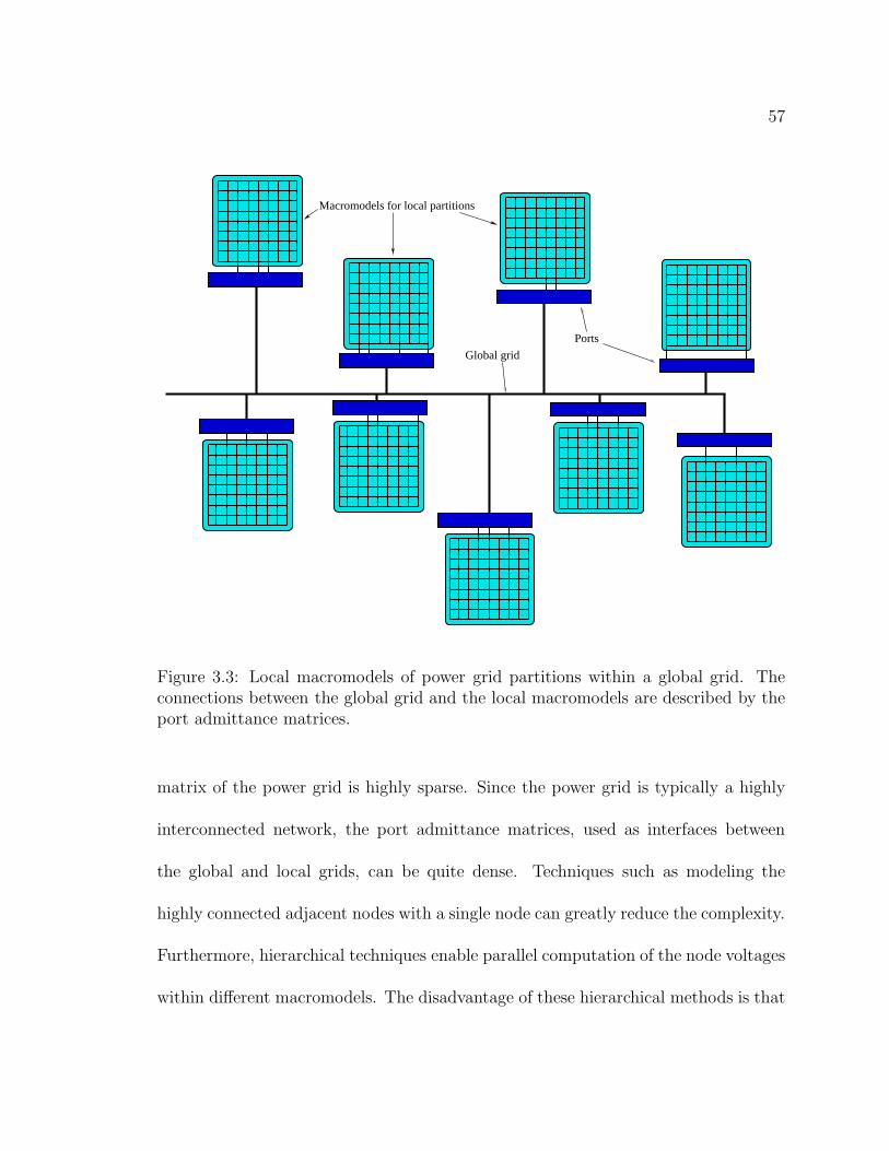
57
Macromodels for local partitions
Ports
Global grid
Figure 3.3: Local macromodels of power grid partitions within a global grid. Theconnections between the global grid and the local macromodels are described by theport admittance matrices.
matrix of the power grid is highly sparse. Since the power grid is typically a highly
interconnected network, the port admittance matrices, used as interfaces between
the global and local grids, can be quite dense. Techniques such as modeling the
highly connected adjacent nodes with a single node can greatly reduce the complexity.
Furthermore, hierarchical techniques enable parallel computation of the node voltages
within different macromodels. The disadvantage of these hierarchical methods is that

58
the macromodels and port admittance matrices are highly sensitive to the partitioning
technique. Additionally, since the resulting matrices are no longer positive definitive,
Cholesky decomposition cannot be used during the analysis process, increasing the
computational runtime of the algorithm.
3.1.2.3 Multigrid Techniques
A partial differential equation (PDE) such as used in multigrid approaches to
analyze power grids is proposed in [132]. A multigrid approach typically has two
steps, 1) relaxing the problem to reduce the high frequency error components with
iterative solvers, and 2) mapping the problem to a coarser grid where the problem can
be solved more efficiently followed by remapping the solution to the original grid [133].
Since power grids are naturally smooth (i.e., the voltage difference between adjacent
nodes is small), the first step is often skipped without significantly degrading the
accuracy of the power grid analysis process. Skipping the relaxation step significantly
reduces the complexity of multigrid approaches used in power grid analysis [132]. A
representative mapping of a fine power grid model onto a coarse power grid model is
illustrated in Fig. 3.4.
The complexity of reducing a fine mesh structure into a coarser mesh structure
and mapping the results from the coarse grid onto the fine grid is lower due to
the uniform structure. Multigrid-like power grid analysis techniques are therefore
59
(a)
(b)
Figure 3.4: Power grids with different resolutions: a) fine power grid and b) coarsepower grid.
appealing in mesh structured power networks. When the power grid exhibits a non-
uniform structure, multigrid approaches can cause random and unforeseen errors. The
errors caused by the irregularity of the power grid can be mitigated by maintaining
track of the irregularity of the power grid during the mapping process [134]. Another
disadvantage of multigrid techniques is that these techniques are flat, meaning that
the entire power grid is analyzed without partitioning. The memory requirements and
computational runtime of the analysis process for large power grids may, however, not
be feasible.
60
Graphics processing units (GPU) have recently been used in power grid analysis
with general purpose CPUs due to the higher computing power and off-chip memory
bandwidth [135–137]. Utilizing a GPU for power grid analysis is, however, nontrivial.
Memory access and computing should be finely balanced to achieve a more efficient
runtime than CPU-based analysis techniques. The irregularity of the power grid is
also typically converted into a regular power grid model to reduce the number of
random memory accesses.
3.1.2.4 Random Walk-Based Power Grid Analysis
The power grid can be modeled as a weighted graph where the impedance between
the adjacent nodes determines the weight of that particular edge. A parallel between
a resistive power grid and a random walk game in an undirected graph has been
drawn [138]. The impedance characteristics within a power grid are transformed into
a set of corresponding transition probabilities, permitting the voltage at a particular
node to be determined statistically.
In a random walk game, a walker starts walking in the streets of a city attempting
to reach one of his homes. The walker starts the game at an arbitrary node with
a certain amount of money. During each turn, the walker chooses a street from the
available streets. The street selection is performed randomly, depending upon the
associated probability function of each street. The walker may spend some of his

61
money after each turn to stay for the night if a hotel exists at that destination. When
the walker reaches one of his homes, a reward is given and the game is over. The
amount of money that the walker has accumulated when he reaches his home is the
output of each game. If this game is performed a sufficiently large number of times,
the average amount of money that the walker has at the end of the game represents
the solution, according to the central limit theorem [139].
In a power grid, the power supply connections are represented as those homes
where the walker is rewarded and when reached, the analysis is over. The streets
are the power grid lines and the probability of choosing a street depends upon the
impedance characteristics of the corresponding power grid. The amount of money
spent at a node depends upon the amount of current sunk at that node. A power grid
and the corresponding random walk game are illustrated in Fig. 3.5. The transition
probability from a node to an adjacent node is determined by dividing the conductance
of a node to an adjacent node by the sum of the conductances from that node to all
adjacent nodes. A hotel is present when a current load is located at a node. The
hotel prices are the current sunk at that node divided by the sum of the conductance
from that node to all adjacent nodes. Note that the game is terminated when the
voltage supply node is reached.
To determine the voltage at a specific node, a random walk game starts from
that node and ends when a voltage supply (or home) is reached. To enhance the
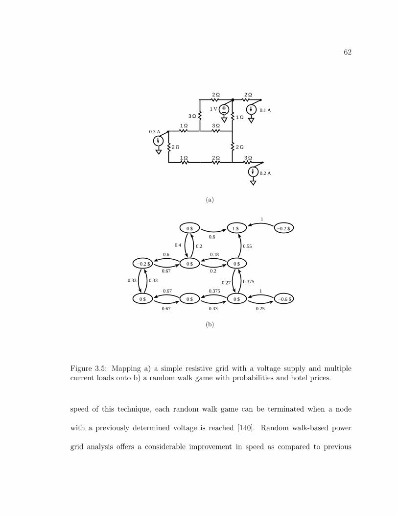
62
3 Ω 1 Ω0.1 A
0.3 A
0.2 A
2 Ω 2 Ω
2 Ω
3 Ω2 Ω1 Ω
1 Ω 3 Ω
1 V
2 Ω
(a)
0 $
0 $
0 $ 0 $ 0 $
0.6
0.4 0.2
0.6
0.33
0.67
0.67
0.375
0.20.67
0.33
0.33
0.375
0.25
1
0.18
0.27
0.55
1
−0.6 $
1 $
0 $−0.2 $
−0.2 $
(b)
Figure 3.5: Mapping a) a simple resistive grid with a voltage supply and multiplecurrent loads onto b) a random walk game with probabilities and hotel prices.
speed of this technique, each random walk game can be terminated when a node
with a previously determined voltage is reached [140]. Random walk-based power
grid analysis offers a considerable improvement in speed as compared to previous

63
techniques. When the number of power supply connections are few, the runtime
of this technique increases significantly. For instance, wire bonded packages offer a
limited number of power supply connections. This technique is therefore less suitable
for power grids with wire bonded packages.
3.2 Summary
Power grid modeling and analysis techniques are reviewed in this chapter. Exam-
ples of direct solvers and iterative techniques are provided. Direct solvers are robust
with minimal convergence issues but in large scale problems require significant mem-
ory to store the system matrices. Iterative solvers can reduce memory requirements,
but may exhibit convergence issues if the system matrix is ill conditioned. Precon-
ditioners are widely used to transform the ill conditioned system matrix into a well
conditioned matrix which is easier to solve [141].
Iterative techniques for power grid analysis either exploit the sparsity of the system
matrix or the special properties of the power grid. Macromodels for small power grid
partitions are analyzed individually and merged with the results of other macromodels
with a global grid in hierarchical power grid analysis techniques. The port admittance
matrices connecting the macromodels to the global grid are highly sensitive and can
be quite dense, greatly increasing the computational runtime of this technique. The
power grid is mapped into a coarse structure. The results of the analysis of this

64
coarse grid is remapped onto the original fine grid in multigrid techniques. Multigrid
techniques can produce random errors when the power grid is not a regular mesh
structure. Additionally, since the entire power grid is analyzed without partitioning,
the memory requirement and computational runtime are typically not feasible for
large power grids. Random walk-based power grid analysis techniques offer an efficient
solution when the number of power supply connections is large. The computational
runtime of this technique is, however, greatly increased when the number of power
supply connections is small.
65
Chapter 4
An Ultra-Small Hybrid VoltageRegulator
The power supply voltage aggressively scales with each technology generation,
making the delivery of a high quality supply voltage to the noise sensitive circuit
blocks highly challenging [13,22,142,143]. The number of voltage domains within an
integrated circuit is increasing to satisfy stringent power budgets. The increase in the
number of voltage domains requires new techniques to generate these voltages close
to the load circuitry while occupying a small amount of area. The power savings
is greater when the voltage regulators are close to the load devices (point-of-load
voltage delivery), making the physical size the primary issue for point-of-load voltage
regulation. Classical power supplies occupy large on-chip area and are therefore not
appropriate for point-of-load power delivery. Several topologies are commonly used
to generate DC voltages for high performance integrated circuits, as discussed in
Chapter 2.
66
Buck converters, which are step-down switching DC-DC converters, are popular
due to the high power efficiency. A second order inductor-capacitor (LC) passive filter
is commonly used in a buck converter. The passive LC components require signifi-
cant on-chip area; therefore, the passive components have generally been implemented
off-chip [18, 22]. As a consequence of placing these components off-chip, significant
voltage droop and bounce are produced at the package level due to the parasitic resis-
tance and inductance between the off-chip components of the voltage converter and
the integrated circuit. Additionally, the parasitic interconnect impedance between
the discrete components of the voltage converter can produce significant power loss.
Furthermore, with power supply scaling, analog and digital circuits are less tolerant
to fluctuations in the supply voltage [18,22]. The parasitic impedance of the intercon-
nect between the discrete components degrades the speed and accuracy of the load
regulation, causing slow response times and changing output voltage levels.
As previously mentioned, the primary issue in the design of a conventional on-
chip voltage converter is the physical area. The on-chip passive LC filter within a
monolithic buck converter occupies a large area. A passive LC filter is therefore
infeasible due to the large area when multiple on-chip voltage converters are needed
(such as in a multi-voltage microprocessor).
A more area efficient voltage converter structure is a low-dropout voltage regu-
lator (LDO) [24, 28, 54, 57–60, 144]. These regulators are implemented on-chip close

67
to the load circuitry for fast and accurate load regulation. These regulators require
a large output capacitance to achieve fast load regulation. This capacitor occupies
significant on-chip area and is therefore generally implemented off-chip [54,144]. The
off-chip output capacitor requires dedicated I/Os and produces higher parasitic losses.
Alternatively, when the output capacitor is placed on-chip, the output capacitor dom-
inates the total LDO regulator area [24]. Many techniques have been proposed to
eliminate the need for the large off-chip capacitor without sacrificing the stability and
performance of the LDO regulator [24,28,57–60]. These techniques, however, do not
completely eliminate the need for an output capacitor. Furthermore, compensation
circuitry that produces a dominant pole requires additional area. Due to the large
area requirement, LDO regulators are not appropriate for a system of distributed
point-of-load voltage regulators.
An ultra-small area efficient voltage converter is required for the next gener-
ation of multi-voltage systems because these systems are highly sensitive to local
power/ground (P/G) noise. The parasitic impedance of the power distribution net-
work is a crucial issue when the voltage converter is far from the load circuitry. Volt-
age converters need to be placed close to the load circuitry since L dI/dt noise and
IR voltage drops have become significant in deeply scaled circuits with aggressively
scaled supply voltages [18, 22].
To produce a voltage regulator appropriate for distributed point-of-load voltage
68
generation, the passive LC filter within a buck converter is replaced with a more area
efficient active filter circuit [145]. A switching input voltage generates the output
voltage and the converter uses a filter structure to produce the desired output volt-
age. The current supplied to the output node, however, does not originate from the
input switching signal; rather, from the operational amplifier (Op Amp) output stage,
similar to a linear voltage converter. The proposed voltage converter is therefore a
hybrid combination of a switching and linear DC-DC converter. The on-chip area of
the proposed hybrid regulator is 0.015 mm2, significantly smaller than state-of-the-
art output capacitorless LDOs. The power efficiency, however, is limited to Vout/Vin,
similar to LDOs.
The rest of the chapter is organized as follows. In Section 4.1, a low pass active
filter based converter is reviewed for different active filter topologies and types such
as Butterworth, Chebyshev, and Bessel. Several tradeoffs among a number of active
filter topologies are discussed. The design requirements of the Op Amp and related
tradeoffs are also discussed in this section. The advantages and disadvantages of the
proposed voltage regulator as compared to conventional switching and LDO regulators
are discussed in Section 4.2. Experimental results are provided in Section 4.3. A
distributed system of point-of-load voltage regulators is described in Section 4.4. A
summary of the chapter is provided in Section 4.5.

69
4.1 Active Filter Based Switching DC-DC Con-
verter Design
In the proposed circuit, the bulky LC filter in a conventional buck converter is
replaced with an active filter structure and the tapered buffers are replaced with
smaller buffers, as shown in Fig. 4.1. The switching input signal generated at Node1
is filtered by the active filter structure, similar to a buck converter, and a DC voltage
is generated at the output. Increasing the duty cycle D of the input switching signal
at Node1 increases the generated DC voltage as in (2.2).
Large tapered buffers are required in a conventional buck converter to drive the
large power transistors, PMOS and NMOS, as shown in Fig. 2.5. The current deliv-
ered to the load circuitry is provided by these large power transistors. In the proposed
circuit, however, the current delivered to the load circuitry is supplied by an oper-
ational amplifier. Small buffers are therefore sufficient for driving the active filter.
Replacing the tapered buffers with smaller buffers significantly decreases the power
dissipated by the input stage. Alternatively, the output buffers within the Op Amp
dissipate power within the regulator. Another characteristic of the regulator is that
the feedback required for line and load regulation is satisfied with separate feedback
paths, as shown in Fig. 4.1. Feedback1 is generated by the active filter structure and
provides load regulation whereas feedback2 is optional and controls the duty cycle
70
Node R R R
C
C
C
Vdd
Pulse width modulator
CircuitsLoad
ActiveFilter
PMOS
NMOS
Node
Vdd
Vdd
Active filter
1 2 3
3
2
1
Feedback
Feedback
2
1
1
1
2
2
1
Figure 4.1: Proposed DC-DC converter. Note that the passive LC filter is replacedwith an active filter and the large tapered buffers are no longer necessary.
of the switching signal for line regulation. In most cases, feedback1 is sufficient to
guarantee fast and accurate load regulation. When only one feedback path is used,
the switching signal is generated by simpler circuitry (e.g., a ring oscillator) and the
duty cycle of the switching signal is compensated by a local feedback circuit (a duty
cycle adjustor). The primary advantage of a single feedback path is smaller area since
feedback1 is produced by the active filter and no additional circuitry is required for
the compensation structure.
Utilizing active filters within a switching voltage regulator to replace the passive
LC filter was first proposed in [145], however, several important design issues such
as power efficiency, the sensitivity of the active filter, the importance of the output
buffer stage of the Op Amp, and the type and topology of the active filter structure

71
were overlooked. Additionally, the active filter-based regulator in [145] requires a 10
µF capacitor, which occupies significant on-chip area and is therefore inappropriate
for point-of-load voltage regulation. Less than 8 pF capacitance is used within the
active filter portion of the proposed voltage regulator for a cutoff frequency of 50
MHz.
Active filters have been well studied over the past several decades [146,147]. The
objective of this section is to review those properties of active filters that affect the
design of the proposed voltage regulator while providing some relevant background
material. Active filter configurations and topologies relevant to the proposed regulator
are reviewed in Section 4.1.1. In Section 4.1.2, the design of the Op Amp circuit is
reviewed.
4.1.1 Active Filter Design
Active filter structures contain no passive inductors. The filtering function uses
capacitors, resistors, and an active circuit (i.e., the Op Amp). Certain design con-
siderations should be considered when utilizing an active filter as a voltage regulator
since the appropriate active filter topology depends upon the application. For a
voltage regulator, the on-chip area requirement, sensitivity of the active filter to com-
ponent parameter variations (due to aging, temperature, and process variations), and
the power dissipated by the active components should be low. Two topologies are

72
VoutVin R R R
C C
C
OscillatorRing
1 2 3
1 3
2
Figure 4.2: Active low pass Sallen-Key filter circuit. No DC current path existsbetween the input and output nodes.
popular for implementing an integrated low pass active filter, multiple feedback and
Sallen-Key [146]. Multiple feedback low pass filters use capacitive and resistive com-
ponents within the feedback path from the output to the input. A DC current path
exists between the input and output nodes due to the resistive feedback. The DC
current increases the power dissipated by the multiple feedback active filter. Multiple
feedback active filters are therefore less suitable for an active filter based on-chip volt-
age regulator. Alternatively, Sallen-Key low pass filters only use capacitive feedback.
Hence, the static power dissipation of the Sallen-Key topology is significantly less
than the multiple feedback topology.
A third order low pass unity-gain Sallen-Key filter topology is shown in Fig. 4.2.
The first section, R1 and C1, forms a first order low pass RC filter. The remaining
components, R2, R3, C2, C3, and the Op Amp, form a second order Sallen-Key low
pass filter. Note that no DC current path exists between the input and output.
The gain of the active filter can be increased by inserting resistive feedback between
the non-inverting input and output nodes, forming a DC current path between the
output and ground. Since low power dissipation is crucial to the proposed circuit, a

73
unity-gain topology is chosen.
The transfer function of the active filter shown in Fig. 4.2 is
Vout
Vin=
1
a1s3 + a2s2 + a3s+ a4, (4.1)
where
a1 = R1R2R3C1C2C3,
a2 = R1C1C3(R2 +R3) +R3C2C3(R1 +R2),
a3 = R1C1 + C3(R1 +R2 +R3),
a4 = 1.
Various filter types exist in the literature with zeros at infinity, for example, Butter-
worth, Chebyshev type I, and Bessel [147]. Other filter types such as Elliptic and
Chebyshev type II filters exhibit faster transition characteristics. Since the Elliptic
and Chebyshev type II filters contain zeros in the transfer function, the Sallen-Key
topology depicted in Fig. 4.2 cannot be used to implement these filters. Zeros can be
produced with more complex feedback structures such as a twin-t or bridged-t cir-
cuit [147]. These structures, however, have resistors connected to ground, increasing
the power dissipated by the active filter.
A Chebyshev type I filter is chosen for the active filter due to the steep roll-off

74
Table 4.1: Sensitivity analysis for a third order Sallen-Key filter. Per cent change incutoff frequency and Q factor when individual parameter values are increased by 1%.
R1 R2 R3 C1 C2 C3Q 0 -0.4 0.4 0 -0.5 0.5
Cut-off frequency -1 -0.5 -0.5 -1 -0.5 -0.5
factor as compared to those filter structures which do not require resistive components
connected to ground to produce finite zeros. The active filter passes the switching
signal at a constant frequency and generates a DC output voltage. A third order
Chebyshev type I low pass Sallen-Key filter, shown in Fig. 4.2, is utilized in the
proposed voltage regulator since no attenuation occurs at DC when the order of the
Chebyshev filter is odd. The per cent change in the cutoff frequency and the Q factor
of the third order Sallen-Key filter, shown in Fig. 4.2, are listed in Table 4.1 for an
increase of 1% in the value of the individual parameters.
4.1.2 Op Amp Design
The performance of an active filter depends strongly on the Op Amp. The gain-
bandwidth (GB) product of the Op Amp determines the bandwidth of the active
filter. Most of the power loss takes place within the Op Amp structure, since the
current provided to the output load is supplied by the Op Amp output stage. Hence,
the Op Amp needs to provide tens of milliamps of current to the load devices while
maintaining sufficient performance to reliably operate the active filter.
75
VinVout
VinP1
N1 N2N3
N4
N5
P3P4
Cc
Vdd
Idc
P5
P2
Figure 4.3: Three stage Op Amp with PMOS input transistors. The PMOS inputtransistors are used in the first differential input stage. The second stage is a common-source gain stage and the third stage forms the output buffer that supplies the currentto the load.
A three stage classical differential-input single-ended CMOS Op Amp structure is
utilized in the proposed regulator, as shown in Fig. 4.3 [148]. A Miller capacitor CC ,
which is 2 pF, is used to ensure stability. The size of the transistors in the output
stage is considerably larger than the first two stages to supply sufficient current to
the load circuits. The first and second stages are gain stages which provide a cascade
gain of greater than 50 dB. The third stage exhibits a gain close to unity, so the
overall three stage gain is close to 50 dB with a phase margin of 51, as depicted in
Fig. 4.4.
76
Phase margin = 51o
Figure 4.4: Magnitude and frequency response of the Op Amp in the active filter.The phase margin is 51.
4.2 Pros and Cons of Active Filter-Based Voltage
Regulator
The proposed voltage regulator is a hybrid combination of a switching and linear
voltage regulator and exhibits certain advantages and disadvantages from using a
combination of a switching and LDO regulator topology.
Voltage regulation: The line and load regulation of the proposed voltage con-
verter is separated into two different feedback paths, as shown in Fig. 4.1. The re-
sponse time for abrupt changes in the load current is faster than a switching regulator
and similar to an LDO regulator. The line regulation characteristics are, however,
similar to a switching voltage regulator where the duty cycle of the input switching
signal is altered by the PWM.

77
Stability: The stability of a buck converter is typically determined by the effective
series resistance (ESR) of the output capacitor. A buck converter can be unstable
when the ESR is too small due to a double pole formed by a second order LC filter.
The proposed regulator uses an NMOS transistor at the output stage of the Op Amp
with a low output impedance where the Miller capacitor (Cc) provides the dominant
pole. During full load condition, i.e., the effective load resistance is small, the stability
is not significantly degraded due to the small effective output impedance. With an
NMOS output stage, the proposed regulator is inherently stable since one of the poles
is at a higher frequency.
On-chip area: The physical area of the proposed regulator is smaller than both
a switching and LDO voltage regulator since there is no large output capacitor. The
frequency of the input switching signal can be increased without significantly degrad-
ing the power efficiency because the buffers delivering this switching signal can be
small. With higher switching frequencies, the size of the proposed regulator can be
further decreased. The primary advantage of the proposed regulator as compared to
other regulator topologies is the small area requirement and further reduced size in
highly scaled technologies without significantly degrading the power efficiency.
Power efficiency: The power efficiency of a buck converter can theoretically
approach 100% when the parasitic impedances are ignored. For an LDO or the
proposed regulator, the maximum attainable power efficiency is limited to Vout/Vin,
78
PWM
Passive RC
Op amp Op amp
output
stage
Output test pad
185 µm
80 µm
Figure 4.5: Die microphotograph of the hybrid voltage regulator.
as previously mentioned.
Maximum load current: The maximum current that can be delivered to the
load depends upon the size of the power transistors (PMOS and NMOS shown in
Fig. 2.5) driving the LC filter. A higher current can be delivered with larger power
transistors. The maximum load current of an LDO regulator depends upon the size
of the pass transistor. Similarly, the maximum load current of the proposed voltage
regulator is determined by the size of the output stage of the Op Amp.
4.3 Experimental Results
The proposed active filter based DC-DC voltage converter has been designed and
fabricated in a 110 nm CMOS technology. The objective of the circuit is an ultra-small
voltage regulator with an area smaller than 0.015 mm2. A significant portion of this
79
area is allocated to the Op Amp, as shown in Fig. 4.5. The active filter, Op Amp, and
PWM are placed in the remaining available area. The active filter is designed within
the available area with a cutoff frequency of approximately 50 MHz. Note that the
cutoff frequency increases when the area of the active filter is reduced. The frequency
of the input switching signal should be greater than the cutoff frequency of the active
filter to not generate a high frequency ripple at the output. From simulation results,
an 80 MHz input switching signal is observed to be sufficiently high to filter out
the high frequency harmonics within the input switching signal. An input switching
frequency greater than 80 MHz is not preferred because a higher switching frequency
would increase the dynamic power dissipation. A ring oscillator supplies a 50% duty
cycle switching signal to the input. Since there is no need for large tapered buffers,
the power dissipated by the ring oscillator and output buffers is relatively small. The
size of the transistors at the output stage of the Op Amp can be changed for different
output voltage or load current demands. The on-chip area of the proposed regulator
therefore depends upon the specific output voltage and load current characteristics.
Boost circuitry is not utilized in the proposed regulator at the gate of the NMOS
source follower because of sufficient margin between the input (1.8 volts) and output
(0.9 volts). A charge pump circuit can be connected to the gate of the source follower
to boost the voltage or, if available, a zero threshold NMOS transistor for the output
source follower stage can be used to increase the gate voltage.
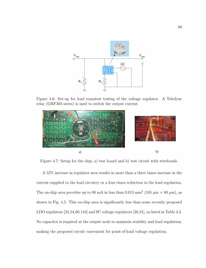
80
Vout
R1 R2
AC
outV
Figure 4.6: Set-up for load transient testing of the voltage regulator. A Teledynerelay (GRF303 series) is used to switch the output current.
a) b)
Figure 4.7: Setup for the chip; a) test board and b) test circuit with wirebonds.
A 52% increase in regulator area results in more than a three times increase in the
current supplied to the load circuitry or a four times reduction in the load regulation.
The on-chip area provides up to 80 mA in less than 0.015 mm2 (185 µm × 80 µm), as
shown in Fig. 4.5. This on-chip area is significantly less than some recently proposed
LDO regulators [24,54,60,144] and SC voltage regulators [30,31], as listed in Table 4.2.
No capacitor is required at the output node to maintain stability and load regulation,
making the proposed circuit convenient for point-of-load voltage regulation.
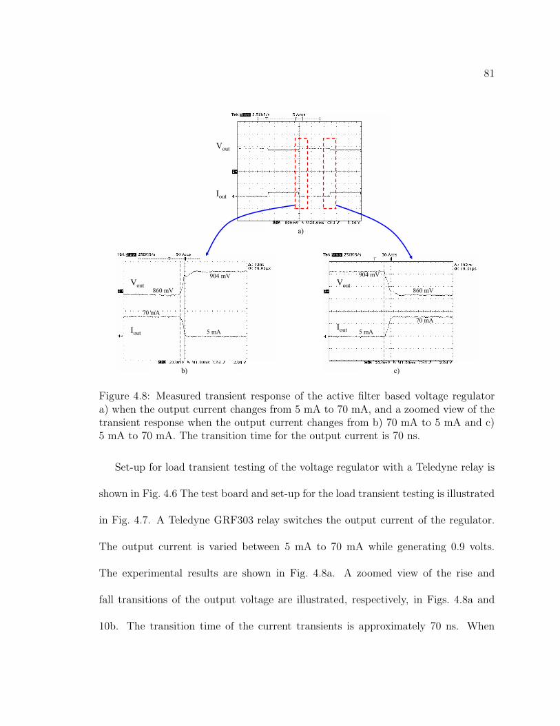
81
Vout
Iout
Vout
Iout
Vout
Iout
70 mA
5 mA 5 mA
70 mA
904 mV
860 mV 860 mV
904 mV
b) c)
a)
Figure 4.8: Measured transient response of the active filter based voltage regulatora) when the output current changes from 5 mA to 70 mA, and a zoomed view of thetransient response when the output current changes from b) 70 mA to 5 mA and c)5 mA to 70 mA. The transition time for the output current is 70 ns.
Set-up for load transient testing of the voltage regulator with a Teledyne relay is
shown in Fig. 4.6 The test board and set-up for the load transient testing is illustrated
in Fig. 4.7. A Teledyne GRF303 relay switches the output current of the regulator.
The output current is varied between 5 mA to 70 mA while generating 0.9 volts.
The experimental results are shown in Fig. 4.8a. A zoomed view of the rise and
fall transitions of the output voltage are illustrated, respectively, in Figs. 4.8a and
10b. The transition time of the current transients is approximately 70 ns. When
82
the output current demand transitions from 5 mA to 70 mA and 70 mA to 5 mA,
the output voltage settles in 72 ns and 192 ns, respectively. Note that no ringing or
overshoot in the output voltage occurs during transient operation, exhibiting highly
stable operation of the voltage regulator with abrupt changes in the output current
demand.
The hybrid voltage regulator dissipates 0.38 mA quiescent current and delivers
up to 80 mA current while generating 0.9 volts from a 1.8 volt input voltage. The
current efficiency is over 99% when the output current demand is greater than 40 mA.
When the output current demand changes, a DC voltage shift occurs in the generated
voltage, as shown in Fig. 4.9. This DC voltage shift at the output of the regulator
is 44 mV when the output current varies between 5 mA and 70 mA, exhibiting a
load regulation of 0.67 mV/mA. With a 52% increase in the voltage regulator area
(i.e., utilizing a larger output buffer), the load regulation can be reduced to ~ 0.17
mV/mA, a fourfold decrease in the DC voltage shift at the output voltage. The
amplitude of this output DC voltage shift depends strongly on the current supplied
to the load circuitry. When the load current demand increases, the effective voltage
across N5 decreases (see Fig. 4.3). This decrease limits the maximum current that N5
can supply to the load for a specific output voltage (or limits the output voltage for
a specific load current demand). Measurements of the load regulation characteristics
of the regulator are illustrated in Fig. 4.10.
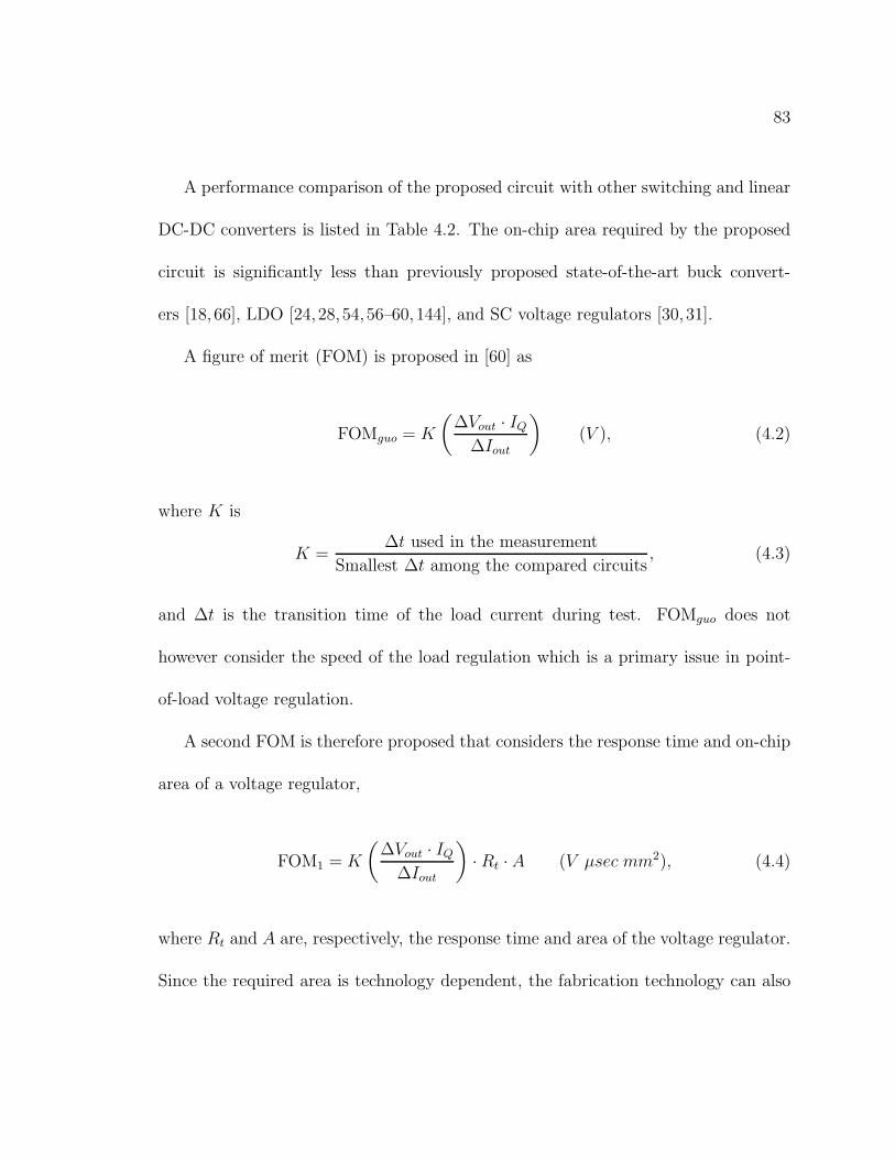
83
A performance comparison of the proposed circuit with other switching and linear
DC-DC converters is listed in Table 4.2. The on-chip area required by the proposed
circuit is significantly less than previously proposed state-of-the-art buck convert-
ers [18, 66], LDO [24, 28, 54, 56–60, 144], and SC voltage regulators [30, 31].
A figure of merit (FOM) is proposed in [60] as
FOMguo = K
(
∆Vout · IQ∆Iout
)
(V ), (4.2)
where K is
K =∆t used in the measurement
Smallest ∆t among the compared circuits, (4.3)
and ∆t is the transition time of the load current during test. FOMguo does not
however consider the speed of the load regulation which is a primary issue in point-
of-load voltage regulation.
A second FOM is therefore proposed that considers the response time and on-chip
area of a voltage regulator,
FOM1 = K
(
∆Vout · IQ∆Iout
)
· Rt · A (V µsec mm2), (4.4)
where Rt and A are, respectively, the response time and area of the voltage regulator.
Since the required area is technology dependent, the fabrication technology can also
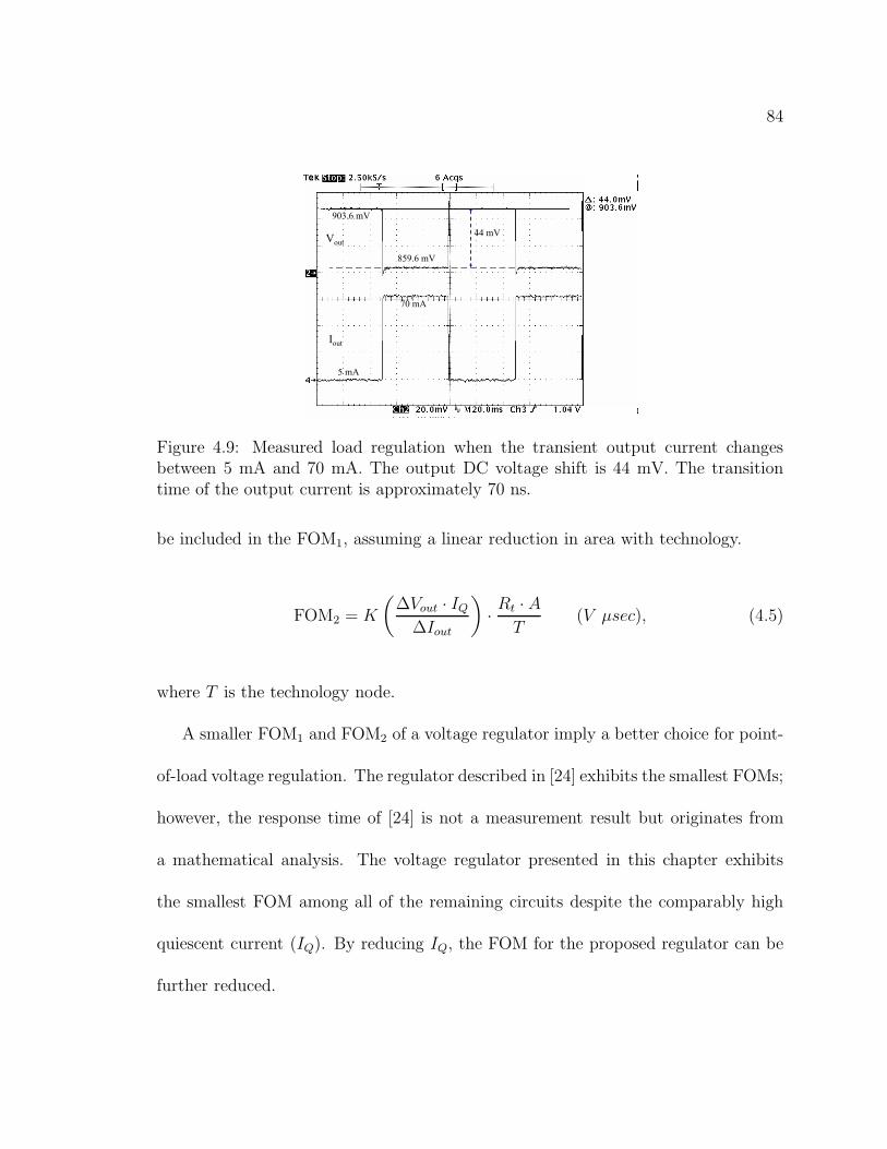
84
Vout
Iout
70 mA
5 mA
859.6 mV
903.6 mV
44 mV
Figure 4.9: Measured load regulation when the transient output current changesbetween 5 mA and 70 mA. The output DC voltage shift is 44 mV. The transitiontime of the output current is approximately 70 ns.
be included in the FOM1, assuming a linear reduction in area with technology.
FOM2 = K
(
∆Vout · IQ∆Iout
)
· Rt · AT
(V µsec), (4.5)
where T is the technology node.
A smaller FOM1 and FOM2 of a voltage regulator imply a better choice for point-
of-load voltage regulation. The regulator described in [24] exhibits the smallest FOMs;
however, the response time of [24] is not a measurement result but originates from
a mathematical analysis. The voltage regulator presented in this chapter exhibits
the smallest FOM among all of the remaining circuits despite the comparably high
quiescent current (IQ). By reducing IQ, the FOM for the proposed regulator can be
further reduced.
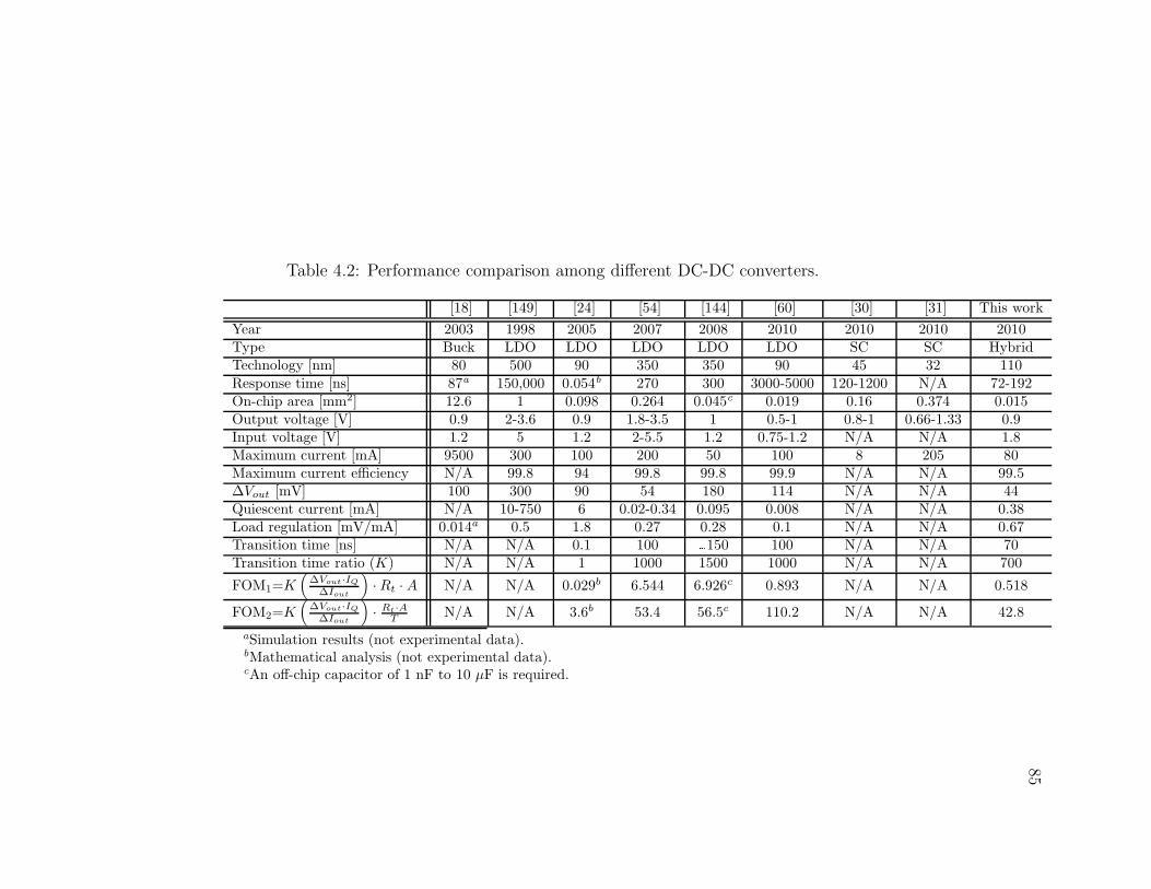
85
Table 4.2: Performance comparison among different DC-DC converters.
[18] [149] [24] [54] [144] [60] [30] [31] This work
Year 2003 1998 2005 2007 2008 2010 2010 2010 2010Type Buck LDO LDO LDO LDO LDO SC SC HybridTechnology [nm] 80 500 90 350 350 90 45 32 110
Response time [ns] 87a 150,000 0.054b 270 300 3000-5000 120-1200 N/A 72-192On-chip area [mm2] 12.6 1 0.098 0.264 0.045c 0.019 0.16 0.374 0.015Output voltage [V] 0.9 2-3.6 0.9 1.8-3.5 1 0.5-1 0.8-1 0.66-1.33 0.9Input voltage [V] 1.2 5 1.2 2-5.5 1.2 0.75-1.2 N/A N/A 1.8Maximum current [mA] 9500 300 100 200 50 100 8 205 80Maximum current efficiency N/A 99.8 94 99.8 99.8 99.9 N/A N/A 99.5∆Vout [mV] 100 300 90 54 180 114 N/A N/A 44Quiescent current [mA] N/A 10-750 6 0.02-0.34 0.095 0.008 N/A N/A 0.38Load regulation [mV/mA] 0.014a 0.5 1.8 0.27 0.28 0.1 N/A N/A 0.67Transition time [ns] N/A N/A 0.1 100 ~150 100 N/A N/A 70Transition time ratio (K) N/A N/A 1 1000 1500 1000 N/A N/A 700
FOM1=K(
∆Vout·IQ∆Iout
)
·Rt · A N/A N/A 0.029b 6.544 6.926c 0.893 N/A N/A 0.518
FOM2=K(
∆Vout·IQ∆Iout
)
· Rt·AT
N/A N/A 3.6b 53.4 56.5c 110.2 N/A N/A 42.8
aSimulation results (not experimental data).bMathematical analysis (not experimental data).cAn off-chip capacitor of 1 nF to 10 µF is required.
86
0 10 20 30 40 50 60 70
860
865
870
875
880
885
890
895
900
905
Output current (mA)
Out
put v
olta
ge (
mV
)
Figure 4.10: Measured load regulation of the proposed circuit is approximately 0.67mV/mA.
The LDO proposed in [149] has a source follower output stage similar to the pro-
posed active filter regulator. A large capacitor C1 and slow control circuitry behaving
as a charge pump are connected to the gate of the NMOS transistor in the source
follower as in [149]. C1 decouples the gate voltage of the NMOS transistor from the
output voltage where voltage variations occur at the source terminal of this transistor.
A larger C1 is therefore needed if the maximum output current demand of the regu-
lator increases whereas only the size of the output NMOS transistor is increased for
the active filter regulator. To provide additional output current, the area is doubled
in [149] as compared to the proposed regulator.
The primary disadvantage of the proposed circuit is that the power efficiency is
limited to Vout/Vin as in a linear voltage regulator. This power loss, however, is
somewhat compensated by replacing the large tapered buffers with smaller buffers
which drive the active filter. Additionally, the filter inductor and capacitor related
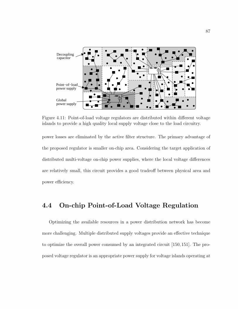
87
Point−of−loadpower supply
Globalpower supply
capacitorDecoupling
Figure 4.11: Point-of-load voltage regulators are distributed within different voltageislands to provide a high quality local supply voltage close to the load circuitry.
power losses are eliminated by the active filter structure. The primary advantage of
the proposed regulator is smaller on-chip area. Considering the target application of
distributed multi-voltage on-chip power supplies, where the local voltage differences
are relatively small, this circuit provides a good tradeoff between physical area and
power efficiency.
4.4 On-chip Point-of-Load Voltage Regulation
Optimizing the available resources in a power distribution network has become
more challenging. Multiple distributed supply voltages provide an effective technique
to optimize the overall power consumed by an integrated circuit [150, 151]. The pro-
posed voltage regulator is an appropriate power supply for voltage islands operating at

88
different supply voltages and clock frequencies. An active filter-based voltage regula-
tor is a favorable choice for point-of-load voltage regulation due to the small area and
flexible drive current to satisfy the local current demand. A representative integrated
circuit with multiple voltage islands is illustrated in Fig. 4.11. Global power supplies
provide the input voltage to the point-of-load voltage regulators. These point-of-load
power supplies generate the required voltages within the different voltage islands.
The number and size of the voltage regulators depend on the load current demand
and output voltage requirements. The proposed voltage regulator can also be used
to generate a clean supply voltage for the noise-sensitive circuit blocks such as the
clock generators [152]. In this case, the number and size of the point-of-load voltage
regulators also depend on the load circuitry.
The resistive IR and inductive di/dt voltage drops are minimized by generating
the supply voltage close to the load circuitry and reducing the parasitic impedances
between the power supply and the load. Additional power savings is also achieved
by reducing the supply voltage within the different voltage islands. The disadvantage
of the proposed design is the large dropout voltage, consequently reducing the power
efficiency. A PMOS output stage, however, can effectively solve this issue without sig-
nificantly increasing the area. In this case, the Op Amp structure should be modified
to drive a PMOS output stage.
89
4.5 Summary
An ultra-small voltage regulator is needed for point-of-load distributed voltage
regulation in high performance integrated circuits. An active filter-based on-chip
DC-DC power supply appropriate for point-of-load voltage regulation is described
in this chapter. The on-chip area of the proposed fully monolithic hybrid voltage
regulator is 0.015 mm2 and provides up to 80 mA output current. The load reg-
ulation is 0.67 mV/mA and the response time ranges from 72 ns to 192 ns. The
area of the regulator is significantly less than previously proposed state-of-the-art
buck converters, LDO, and SC voltage regulators despite a mature 110 nm CMOS
technology. The area of the proposed regulator will therefore be significantly smaller
with more advanced technologies. The need for an off-chip capacitor or advanced
on-chip compensation techniques to satisfy stability and performance requirements
is eliminated in the proposed circuit. This circuit therefore provides a means for
distributing multiple power supplies close to the load to reduce power/ground noise
while enhancing circuit performance by delivering a high quality supply voltage to
the load circuitry. With the proposed voltage regulator, on-chip signal and power
integrity is significantly enhanced with the capability of distributing multiple on-chip
power supplies.

90
Chapter 5
Effective Resistance in a TwoLayer Mesh
An on-chip power and ground distribution network is commonly modeled as a
resistive mesh structure with different vertical and horizontal unit resistances, as
shown in Fig. 5.1a [13, 132, 153, 154], where the thickness and width of the metal
lines are typically different in orthogonal metal layers. Power and ground networks
are illustrated in Fig. 5.1a with, respectively, dark and light grey lines. A mesh
structured power network and the corresponding resistive circuit model are illustrated,
respectively, in Figs. 5.1b and 5.1c. Since the power and ground distribution networks
exhibit similar characteristics, only the power network is considered in this chapter.
This approach can also be used to determine the effective resistance in any two layer
mesh structure with different horizontal and vertical unit resistances.

91
The effective resistance of a mesh is used in power grid analysis [155–157], sub-
strate analysis [158], decoupling capacitance allocation [111, 159, 160], power dissi-
pation [161] and ESD analysis [161], and measuring resistance variations in power
distribution networks [162]. The effective resistance is used to determine the effective
region of a decoupling capacitor [159, 163]. For instance, the effective resistance be-
tween hot spots and available white spaces in a circuit floorplan provides a means to
evaluate the effectiveness of a decoupling capacitor placed at different locations. A
lower effective resistance between a hot spot and decoupling capacitor leads to a faster
response time for the decoupling capacitor. Additionally, the effective resistance be-
tween a decoupling capacitor and power supply connection provides an estimate of
the recharge time of the capacitor. When the effective resistance between two circuit
blocks decreases, noise coupling through the power network increases which can now
be quantified by the effective resistance described in this chapter. The effective re-
sistance is also used to determine the coverage and commute times of a random walk
in a graph [164]. In an undirected resistive graph, the effective resistance is used to
determine the effective chemical distance between bonds, as in [165]. The effective
resistance is also used in distributive control and estimation such as synchronization
and localization of sensor networks [166].
Venezian in [167] developed a closed-form expression of the resistance of a uni-
form mesh where the vertical and horizontal unit resistances are the same. The work
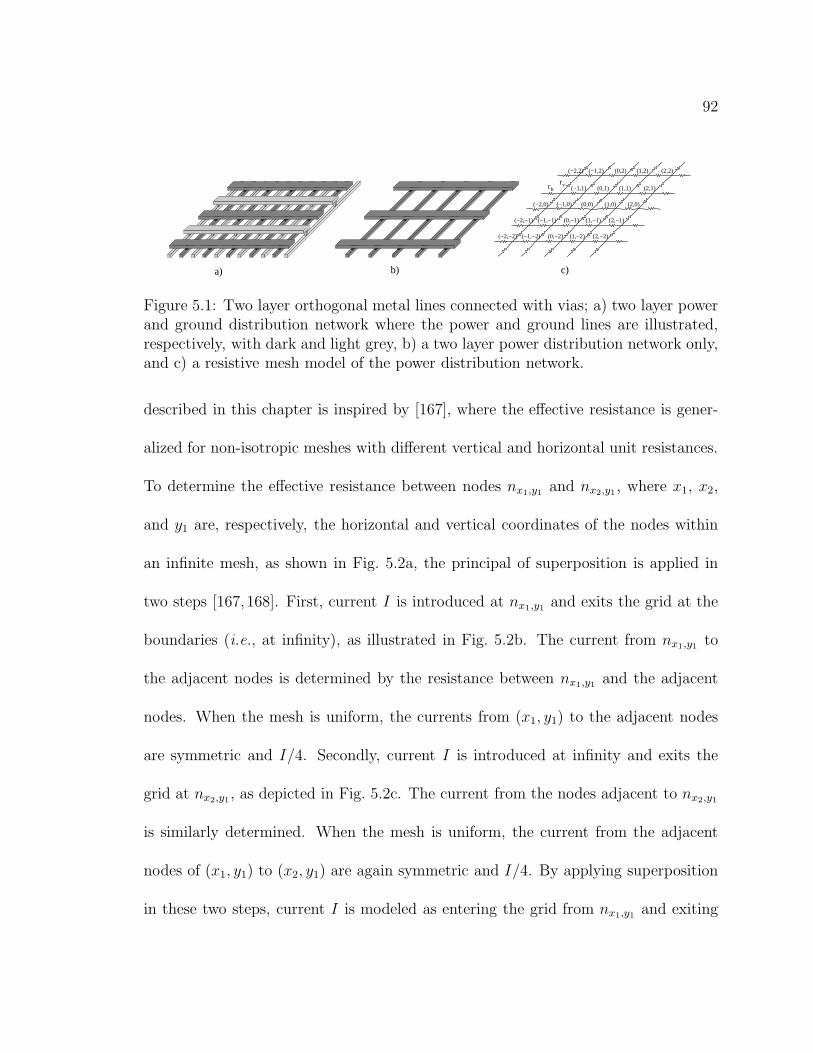
92
rvrh
(1,0) (2,0)(−2,0)
(1,1) (2,1)(0,1)
(0,2)(−2,2)
(0,0)
(2,2)(1,2)(−1,2)
(−1,1)
(−1,0)
(2,−1)(1,−1)(0,−1)(−1,−1)(−2,−1)
(2,−2)(1,−2)(0,−2)(−1,−2)(−2,−2)
a) b) c)
Figure 5.1: Two layer orthogonal metal lines connected with vias; a) two layer powerand ground distribution network where the power and ground lines are illustrated,respectively, with dark and light grey, b) a two layer power distribution network only,and c) a resistive mesh model of the power distribution network.
described in this chapter is inspired by [167], where the effective resistance is gener-
alized for non-isotropic meshes with different vertical and horizontal unit resistances.
To determine the effective resistance between nodes nx1,y1 and nx2,y1 , where x1, x2,
and y1 are, respectively, the horizontal and vertical coordinates of the nodes within
an infinite mesh, as shown in Fig. 5.2a, the principal of superposition is applied in
two steps [167, 168]. First, current I is introduced at nx1,y1 and exits the grid at the
boundaries (i.e., at infinity), as illustrated in Fig. 5.2b. The current from nx1,y1 to
the adjacent nodes is determined by the resistance between nx1,y1 and the adjacent
nodes. When the mesh is uniform, the currents from (x1, y1) to the adjacent nodes
are symmetric and I/4. Secondly, current I is introduced at infinity and exits the
grid at nx2,y1, as depicted in Fig. 5.2c. The current from the nodes adjacent to nx2,y1
is similarly determined. When the mesh is uniform, the current from the adjacent
nodes of (x1, y1) to (x2, y1) are again symmetric and I/4. By applying superposition
in these two steps, current I is modeled as entering the grid from nx1,y1 and exiting

93
the grid at nx2,y1 , as shown in Fig. 5.2d. This current is the sum of the currents
in the first and second steps of the superposition process, which is therefore I/2.
The voltage difference divided by the current is the effective resistance. The effective
resistance between nx1,y1 and nx2,y1 within a uniform mesh is therefore
Reff = 2(Vx1,y1 − Vx2,y1)/I. (5.1)
A similar analysis is performed for a non-isotropic mesh structure with different hor-
izontal and vertical resistances to determine closed-form expressions for the effective
resistance between two arbitrary nodes.
This chapter is organized as follows. In Section 5.1, Kirchhoff’s current law is
revisited to determine the voltages and currents at a particular node in terms of the
neighboring node voltages and resistances. In Section 5.2, inhomogeneous differential
equations are applied where separation of variables is used to determine the node
voltages. The effective resistance between two arbitrary intersections and the corre-
sponding closed-form expressions are described, respectively, in Sections 5.3 and 5.4.
The accuracy of the effective resistance model is discussed in Section 5.5. The chap-
ter is summarized in Section 5.6. A derivation of the closed-form expression for the
effective resistance is offered in Appendix A.

94
1 1x ,y 2 1x ,y
II
(a)
2 1x ,y1 1x ,y node at infinity
I II/4
I/4
I/4I/4
I/4I/4
I/4I/4
(b)
1 1x ,y 2 1x ,y node at infinity
I
I/4
I/4I/4
I/4I/4
I/4I/4
I/4
I
(c)
1 1x ,y 2 1x ,y
I
I/2
I
(d)
Figure 5.2: In an infinite mesh structure: a) a current source I is connected to (x1, y1)and a current load I is connected to (x1, y2) and the effective resistance between theseadjacent nodes is determined by applying the principle of superposition in two steps.In the first step, b) the load current is moved to a node at infinity and in the secondstep, c) the source current is moved to a node at infinity. The current profiles forthese two cases are obtained and d) the current source and load are moved to theoriginal positions and the current during the two superposition steps is summed todetermine the effective resistance.
5.1 Kirchhoff’s Current Law Revisited
The mesh circuit model considered in this chapter is shown in Fig. 5.1c with
horizontal (rh) and vertical (rv) resistors. The voltage at node (x,y) nx,y is Vx,y and
the current from nx,y to ground is Ix,y. When a current source is connected to nx,y,
Ix,y = I. Alternatively, when no current source is connected to nx,y, Ix,y = 0.

95
The current load at an arbitrary node nx,y can be written in terms of the sum of
the current from the four adjacent nodes as
Ix,y =Vx,y−Vx,y+1
rv+Vx,y−Vx,y−1
rv
+Vx,y−Vx+1,y
rh+Vx,y−Vx−1,y
rh. (5.2)
The vertical resistance between adjacent nodes is r and the horizontal resistance
between adjacent nodes is k ∗ r, where k is a number 0 < k < ∞, as
rv = r (5.3)
rh = k ∗ r. (5.4)
When Ix,y = 0, the voltage at nx,y is
Vx,y =kVx,y+1 + kVx,y−1 + Vx+1,y + Vx−1,y
2k + 2. (5.5)
When a current source is connected to nx,y, this current can be described in terms of
the adjacent node voltages and corresponding resistors as
Ix,y=(2k+2)Vx,y−(kVx,y+1+kVx,y−1+Vx+1,y+Vx−1,y)
k r. (5.6)

96
5.2 Separation of Variables
The difference equations, (5.5) and (5.6), can be solved by applying separation of
variables [167]. A solution for (5.5) is
Vx,y = exα+jyβ. (5.7)
By substituting (5.7) into (5.5), (5.5) can be written as
(2k + 2)exα+jyβ = exα+jyβ(kejβ + ke−jβ + eα + e−α), (5.8)
2k + 2 = k(ejβ + e−jβ) + (eα + e−α). (5.9)
Using the cosine and sine properties, (5.9) is
k + 1 = kcosβ + coshα. (5.10)
When a current source is connected to n0,0 and is assumed to exit the system at
infinity, the following equations are satisfied due to symmetry of the mesh structure,
Vx,y = V−x,y = Vx,−y = V−x,−y. (5.11)

97
One possible solution to (5.11) is
Vx,y = e−|x|αcosyβ. (5.12)
The currents can be described in terms of these voltages. Substituting x = y = 0
into (5.6), the current i0,0 at n0,0 is
i0,0 =(2k + 2)V0,0 − kV0,1 − kV0,−1 − V1,0 − V−1,0
kr. (5.13)
Substituting (5.12) into (5.13), the current I at n0,0 is
i0,0 = 2(k + 1− kcosβ − e−α)/kr. (5.14)
Substituting (5.10) into (5.14), the current at n0,0 is
i0,0 = (2coshα− 2e−α)/kr. (5.15)
Using the identities, coshx = 1/2(ex + e−x) and sinhx = 1/2(ex − e−x), from Euler’s
formula [169], the current expression i0,0 becomes
i0,0 = 2sinhα/kr. (5.16)

98
Similarly, when y 6= 0, the current i0,y at n0,y is
i0,y=(2k + 2)V0,y−kV0,y+1−kV0,y−1−V1,y−V−1,y
kr, (5.17)
and substituting (5.10) into (5.17), the current can be rewritten as
i0,y = ((2k + 2)cosyβ − e−αcosyβ − e−αcosyβ − kcos(y + 1)β − kcos(y − 1)β)/kr.
(5.18)
After applying certain trigonometric identities and simplifications,
i0,y =(
(2k + 2− 2e−α)cosyβ − 2kcosyβ cosβ)
/kr. (5.19)
The current i0,y at n0,y is
i0,y = 2(k + 1− e−α − kcosβ)cosyβ/kr. (5.20)
Substituting (5.10) into (5.20) and applying Euler’s formula, the current at n0,y is
i0,y =2sinhα cosyβ
kr. (5.21)

99
5.3 Effective Resistance between Two Nodes
The voltage at nx,y is a function of α and β where the relationship between these
two parameters in (5.10) is in terms of k. The voltage at an arbitrary node nx,y is
the sum of all β values,
Vx,y =
∫ π
0
F (β) vx,y(β) dβ, (5.22)
where F (β) is a function that satisfies a current source at n0,0, and no current source
at n0,y when y 6= 0. Thus, all of the current sources other than at n0,0 are effectively
eliminated [167]. The corresponding current at nx,y is
Ix,y =
∫ π
0
F (β) ix,y(β) dβ. (5.23)
The current at n0,0, by substituting (5.16) into (5.23), is
I0,0 =
∫ π
0
F (β)2sinhα
kdβ, (5.24)
and the current at n0,y, by substituting (5.21) into (5.23), is
I0,n =
∫ π
0
F (β)2sinhα cosyβ
kdβ. (5.25)
100
From inspection, F (β) is
F (β) =k I r
2π sinhα, (5.26)
to satisfy (5.22) when only one current source located at n0,0 is present within the
mesh. Substituting (5.26) and (5.12) into (5.22), the voltage at nx,y is
Vx,y =k I r
2π
∫ π
0
e−|x|α cosyβ
sinhαdβ. (5.27)
5.4 Closed-Form Expression of the Effective Re-
sistance
The effective resistance of a mesh between n0,0 and nx,y is
Rx,y = 2(V0,0 − Vx,y)/I, (5.28)
as discussed previously. Substituting (5.27) into (5.28), the effective resistance be-
tween n0,0 and nx,y is
Rx,y =k r
π
∫ π
0
(2− e−|x|α cosyβ)
sinhαdβ. (5.29)

101
Rx,y is solved by dividing the integral into two, and writing (5.29) as a sum of two
integrals, Rx,y/r = R1(x,y) +R2(x,y),
Rx,y/r =
√k
π
∫ π
0
(1− e−x√k|β| cosyβ)
βdβ +
k
π
∫ π
0
[1
√
(k + 1− k cosβ)2 − 1− 1
β√k]dβ.
(5.30)
The first integralR1(x,y) is rewritten in terms of the exponential integral Ein(z) [169],
Ein(z) =
∫ z
0
1− e−t
tdβ, (5.31)
and R1(x,y) is
R1(x,y) = (1/πk)Re
Ein[π(√kx+ iy)]
. (5.32)
(5.32) is numerically solved and R1(x,y) is
R1(x,y) =
√k
2π[ln(x2 + ky2) + 2(0.57721 + lnπ)], (5.33)
while the second integral R2(x,y) is determined assuming k = n+ ǫ.
R2(x,y) =k
π
∫ π
0
(
(
(n+ 1− ncosβ)2 − 1)−1/2 − 1
β√n
)
dβ
+k
π
∫ π
0
(
−ǫ(1− cosβ)(n+ 1− ncosβ)
((n + 1− ncosβ)2 − 1)3/2+
ǫ
2βn√n
)
dβ. (5.34)
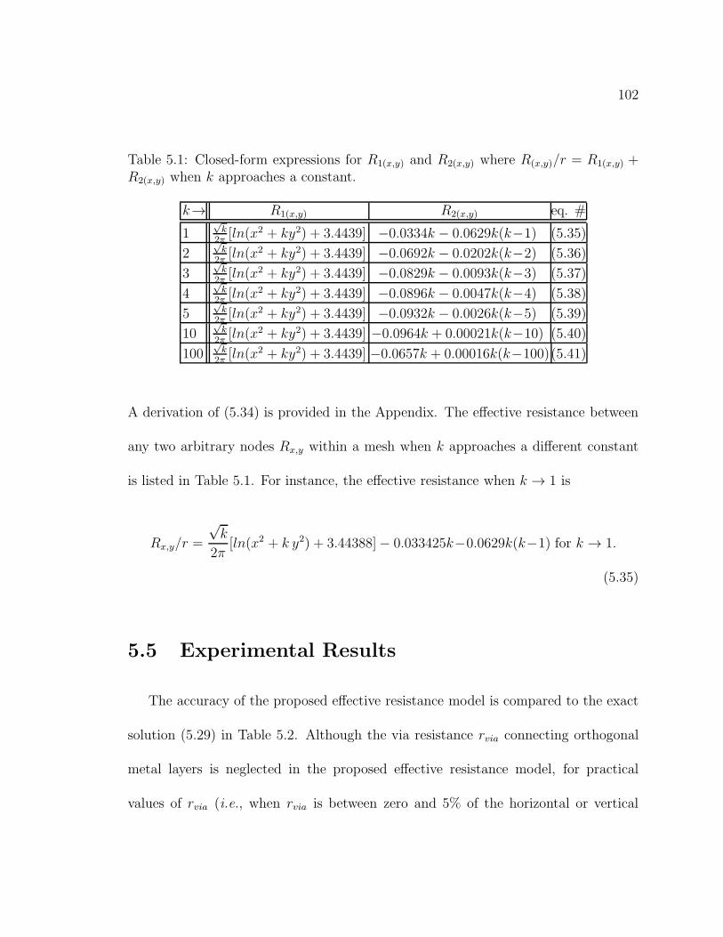
102
Table 5.1: Closed-form expressions for R1(x,y) and R2(x,y) where R(x,y)/r = R1(x,y) +R2(x,y) when k approaches a constant.
k→ R1(x,y) R2(x,y) eq. #
1√k
2π[ln(x2 + ky2) + 3.4439] −0.0334k − 0.0629k(k−1) (5.35)
2√k
2π[ln(x2 + ky2) + 3.4439] −0.0692k − 0.0202k(k−2) (5.36)
3√k
2π[ln(x2 + ky2) + 3.4439] −0.0829k − 0.0093k(k−3) (5.37)
4√k
2π[ln(x2 + ky2) + 3.4439] −0.0896k − 0.0047k(k−4) (5.38)
5√k
2π[ln(x2 + ky2) + 3.4439] −0.0932k − 0.0026k(k−5) (5.39)
10√k
2π[ln(x2 + ky2) + 3.4439] −0.0964k + 0.00021k(k−10) (5.40)
100√k
2π[ln(x2 + ky2) + 3.4439] −0.0657k + 0.00016k(k−100)(5.41)
A derivation of (5.34) is provided in the Appendix. The effective resistance between
any two arbitrary nodes Rx,y within a mesh when k approaches a different constant
is listed in Table 5.1. For instance, the effective resistance when k → 1 is
Rx,y/r =
√k
2π[ln(x2 + k y2) + 3.44388]− 0.033425k−0.0629k(k−1) for k → 1.
(5.35)
5.5 Experimental Results
The accuracy of the proposed effective resistance model is compared to the exact
solution (5.29) in Table 5.2. Although the via resistance rvia connecting orthogonal
metal layers is neglected in the proposed effective resistance model, for practical
values of rvia (i.e., when rvia is between zero and 5% of the horizontal or vertical
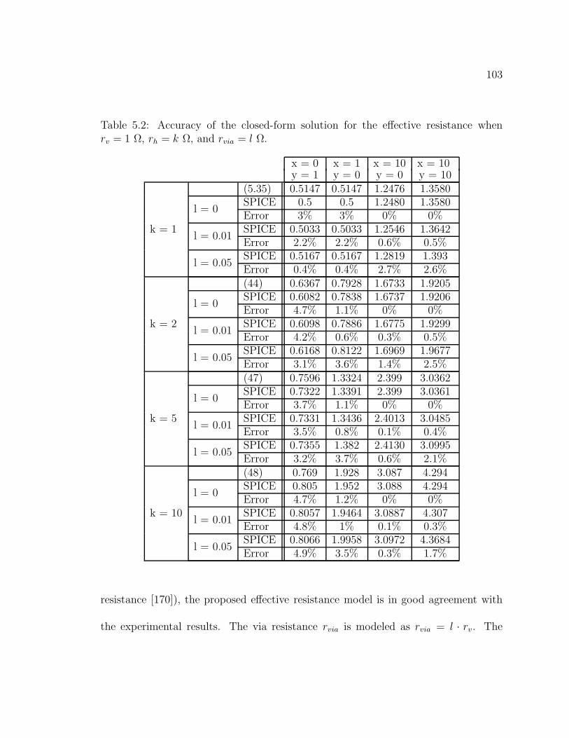
103
Table 5.2: Accuracy of the closed-form solution for the effective resistance whenrv = 1 Ω, rh = k Ω, and rvia = l Ω.
x = 0 x = 1 x = 10 x = 10y = 1 y = 0 y = 0 y = 10
k = 1
(5.35) 0.5147 0.5147 1.2476 1.3580
l = 0SPICE 0.5 0.5 1.2480 1.3580Error 3% 3% 0% 0%
l = 0.01SPICE 0.5033 0.5033 1.2546 1.3642Error 2.2% 2.2% 0.6% 0.5%
l = 0.05SPICE 0.5167 0.5167 1.2819 1.393Error 0.4% 0.4% 2.7% 2.6%
k = 2
(44) 0.6367 0.7928 1.6733 1.9205
l = 0SPICE 0.6082 0.7838 1.6737 1.9206Error 4.7% 1.1% 0% 0%
l = 0.01SPICE 0.6098 0.7886 1.6775 1.9299Error 4.2% 0.6% 0.3% 0.5%
l = 0.05SPICE 0.6168 0.8122 1.6969 1.9677Error 3.1% 3.6% 1.4% 2.5%
k = 5
(47) 0.7596 1.3324 2.399 3.0362
l = 0SPICE 0.7322 1.3391 2.399 3.0361Error 3.7% 1.1% 0% 0%
l = 0.01SPICE 0.7331 1.3436 2.4013 3.0485Error 3.5% 0.8% 0.1% 0.4%
l = 0.05SPICE 0.7355 1.382 2.4130 3.0995Error 3.2% 3.7% 0.6% 2.1%
k = 10
(48) 0.769 1.928 3.087 4.294
l = 0SPICE 0.805 1.952 3.088 4.294Error 4.7% 1.2% 0% 0%
l = 0.01SPICE 0.8057 1.9464 3.0887 4.307Error 4.8% 1% 0.1% 0.3%
l = 0.05SPICE 0.8066 1.9958 3.0972 4.3684Error 4.9% 3.5% 0.3% 1.7%
resistance [170]), the proposed effective resistance model is in good agreement with
the experimental results. The via resistance rvia is modeled as rvia = l · rv. The
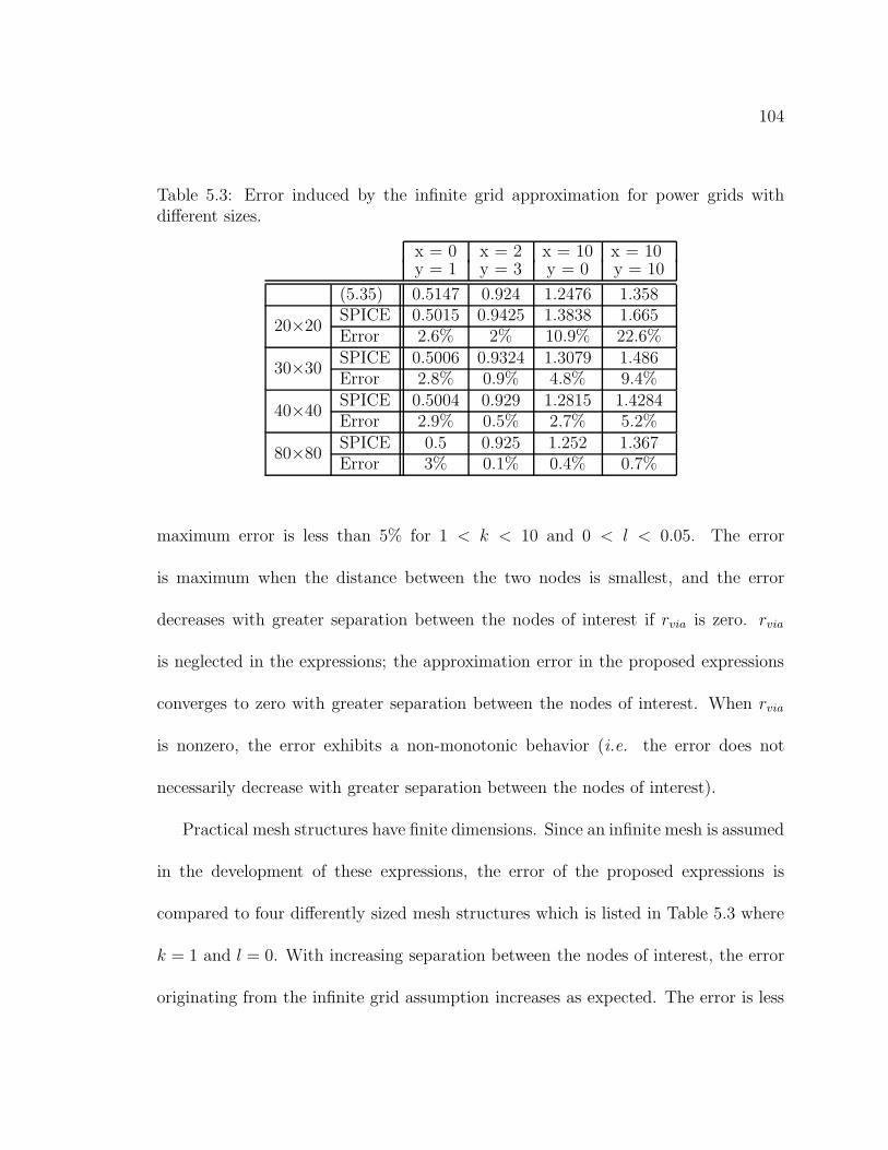
104
Table 5.3: Error induced by the infinite grid approximation for power grids withdifferent sizes.
x = 0 x = 2 x = 10 x = 10y = 1 y = 3 y = 0 y = 10
(5.35) 0.5147 0.924 1.2476 1.358
20×20SPICE 0.5015 0.9425 1.3838 1.665Error 2.6% 2% 10.9% 22.6%
30×30SPICE 0.5006 0.9324 1.3079 1.486Error 2.8% 0.9% 4.8% 9.4%
40×40SPICE 0.5004 0.929 1.2815 1.4284Error 2.9% 0.5% 2.7% 5.2%
80×80SPICE 0.5 0.925 1.252 1.367Error 3% 0.1% 0.4% 0.7%
maximum error is less than 5% for 1 < k < 10 and 0 < l < 0.05. The error
is maximum when the distance between the two nodes is smallest, and the error
decreases with greater separation between the nodes of interest if rvia is zero. rvia
is neglected in the expressions; the approximation error in the proposed expressions
converges to zero with greater separation between the nodes of interest. When rvia
is nonzero, the error exhibits a non-monotonic behavior (i.e. the error does not
necessarily decrease with greater separation between the nodes of interest).
Practical mesh structures have finite dimensions. Since an infinite mesh is assumed
in the development of these expressions, the error of the proposed expressions is
compared to four differently sized mesh structures which is listed in Table 5.3 where
k = 1 and l = 0. With increasing separation between the nodes of interest, the error
originating from the infinite grid assumption increases as expected. The error is less

105
than 3% when the nodes of interest are twenty lines away from the boundary.
5.6 Summary
A closed-form expression for the effective resistance of a two layer mesh structure
is presented in this chapter. The unit resistance of the horizontal and vertical metal
lines within a power grid is often different in adjacent orthogonal metal layers due
to the difference in the width and thickness of these metal lines. The closed-form
expression presented in this chapter uses a parameter k to model the ratio of the
horizontal and vertical resistances. These closed-form expressions provide a fast and
accurate solution to the effective resistance of a two layer mesh which can be used
to solve a variety of problems found in different disciplines. Examples include IR
voltage drop analysis of integrated circuits, synchronization and localization of sensor
networks, the effective chemical distance between bonds, metal mesh interference
filters in terahertz physics, and the commute and cover times of undirected graphs.
106
Chapter 6
Fast Algorithms For IR VoltageDrop Analysis
Several methods have been proposed for efficient power grid analysis as described
in Chapter 3, reduce the size of the linear system, iteratively solve the linear system,
and apply advanced linear algebraic techniques to exploit the sparse nature of the
power grid. Although these algorithms are faster than conventional linear solvers,
significant computational time is required to iteratively apply these algorithms. An
accurate closed-form expression would effectively solve this problem.
Although the interactions between the power supplies and load circuitry occur
globally, these interactions are more prominent among components physically close
to each other. A power supply connection in a multi-voltage system on one side of an
IC has little effect on a circuit block at the other side of the IC. Alternatively, current
provided by a power network is generally distributed to nearby circuit blocks. This
phenomenon is due to the principle of spatial locality [171]. With this principle, a

107
power grid can be partitioned to enhance the overall power grid analysis process.
Uniform current loads are generally assumed in power distribution networks to
exploit symmetry in a linear system. In [172], an IR drop analysis algorithm is de-
scribed for a power grid structure with semi-uniform current loads (e.g., uniform load
currents are assumed within each quadrant of the distribution network). Closed-form
expressions for the maximum IR drop are described in [173], assuming a uniform cur-
rent distribution. Until these results, no closed-form expressions existed to describe
the voltage drop at any point in a locally uniform, globally non-uniform power dis-
tribution network with non-uniform current loads and non-uniform voltage supplies.
In this chapter, fast algorithms for IR drop analysis based on an effective resis-
tance, is provided for locally uniform, globally non-uniform power grids with non-
uniform current loads and non-uniform voltage supplies. The proposed algorithm
exploits the impedance characteristics of the power distribution network and the
effective impedance between the active circuit blocks to provide these closed-form
expressions. The effective impedance between two points in a semi-uniform grid
structure is described in the previous chapter, permitting the resistance between any
two points in a resistive grid to be formulated. Since no iterations are required to
compute the IR drop at any particular node, the proposed algorithm outperforms
previously proposed techniques with reasonable error. The principle of locality is also
applied to accelerate the analysis process.
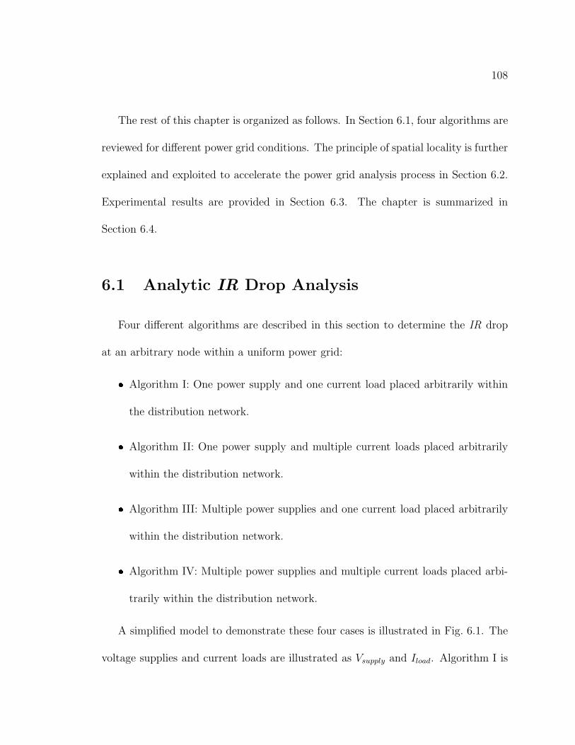
108
The rest of this chapter is organized as follows. In Section 6.1, four algorithms are
reviewed for different power grid conditions. The principle of spatial locality is further
explained and exploited to accelerate the power grid analysis process in Section 6.2.
Experimental results are provided in Section 6.3. The chapter is summarized in
Section 6.4.
6.1 Analytic IR Drop Analysis
Four different algorithms are described in this section to determine the IR drop
at an arbitrary node within a uniform power grid:
Algorithm I: One power supply and one current load placed arbitrarily within
the distribution network.
Algorithm II: One power supply and multiple current loads placed arbitrarily
within the distribution network.
Algorithm III: Multiple power supplies and one current load placed arbitrarily
within the distribution network.
Algorithm IV: Multiple power supplies and multiple current loads placed arbi-
trarily within the distribution network.
A simplified model to demonstrate these four cases is illustrated in Fig. 6.1. The
voltage supplies and current loads are illustrated as Vsupply and Iload. Algorithm I is
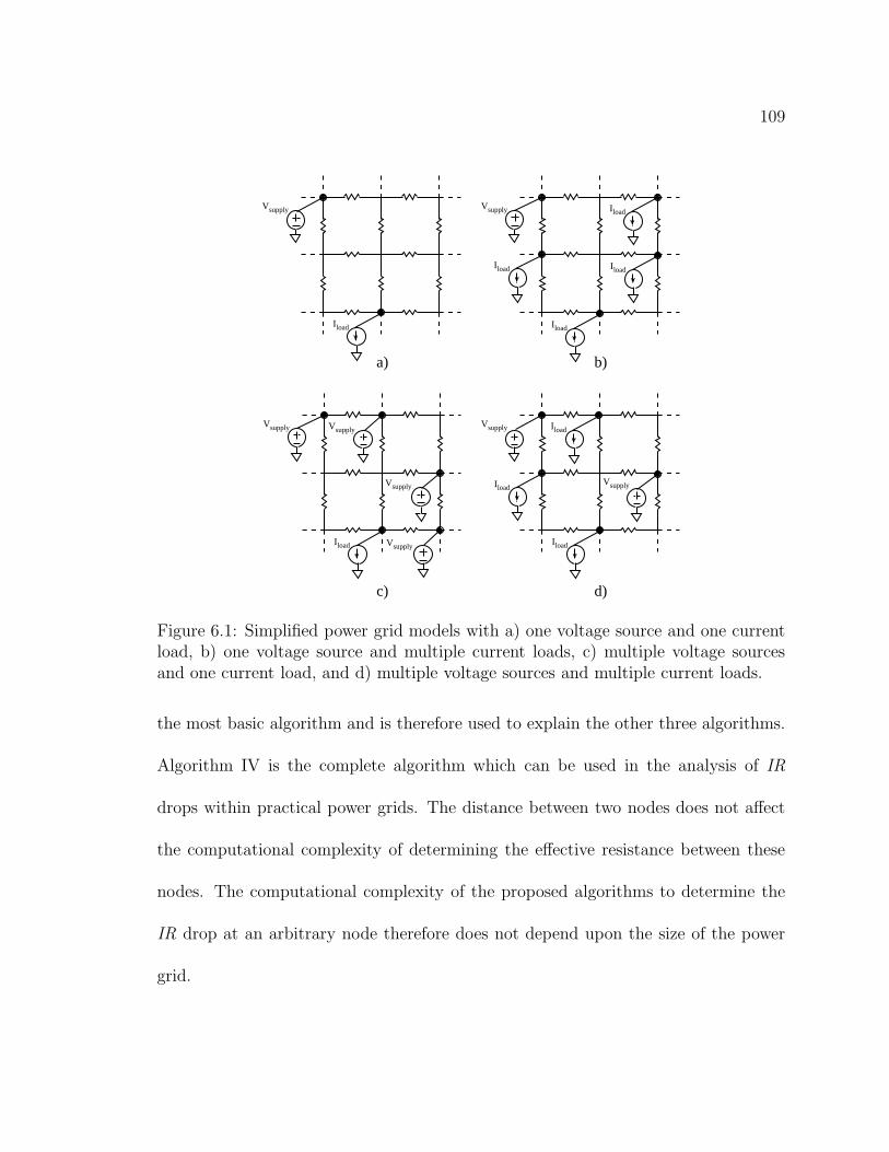
109
Vsupply
Vsupply
Vsupply
Vsupply
I load
I load
Vsupply
I load
Vsupply
I load I load
I loadVsupply
I load
I loadI load
Vsupply
b)a)
c) d)
Figure 6.1: Simplified power grid models with a) one voltage source and one currentload, b) one voltage source and multiple current loads, c) multiple voltage sourcesand one current load, and d) multiple voltage sources and multiple current loads.
the most basic algorithm and is therefore used to explain the other three algorithms.
Algorithm IV is the complete algorithm which can be used in the analysis of IR
drops within practical power grids. The distance between two nodes does not affect
the computational complexity of determining the effective resistance between these
nodes. The computational complexity of the proposed algorithms to determine the
IR drop at an arbitrary node therefore does not depend upon the size of the power
grid.

110
6.1.1 One power supply and one current load
In this section, the IR voltage drop at an arbitrary node Node1, shown in Fig. 6.2a,
is determined when one power supply and one current load exist within the power
grid. The power grid model, shown in Fig. 6.2a, reduces to an effective resistance
model to determine the voltages at Nload and Node1, as illustrated, respectively, in
Figs. 6.2b and 6.2c. The effective resistance between Nsupply and Node1, Node1 and
Nload, and Nsupply and Nload is denoted, respectively, as Rsn, Rnl, and Rsl. These
effective resistances are determined either using the closed-form effective resistance
expressions proposed in Chapter 5 if the power grid exhibits a semi-uniform structure
or using the effective resistance models proposed in [174] for non-uniform power grids.
The voltage at Nload is
Vload = Vsupply − Iload ∗Rsl. (6.1)
After determining the voltage at Nload (see Fig. 6.2a), the voltage at Node1 can be
found using the principle of superposition for the effective resistance model illustrated
in Fig. 6.2c,
VNode1 = Vsupply ∗Rnl
Rsn +Rnl+ Vload ∗
Rsn
Rsn +Rnl. (6.2)
Assuming the current i, depicted in Fig. 6.2, is
i =Vsupply − Vload
Rsn +Rnl, (6.3)
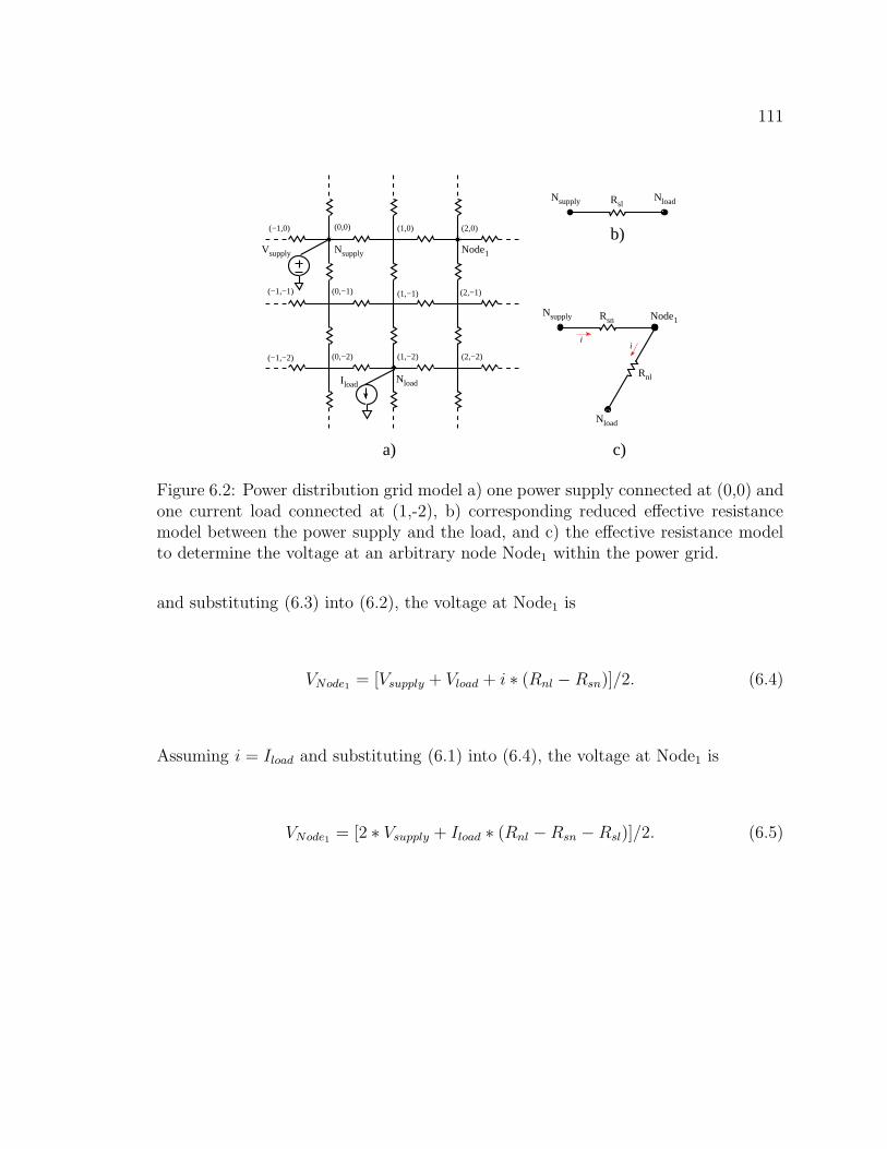
111
I load
Node1
Nload
Nsupply
Nload
Nsupply Node1
Rnl
Rsn
c)
Nsupply NloadRsl
b)
(2,−2)(1,−2)(0,−2)(−1,−2)
(2,−1)(1,−1)(0,−1)(−1,−1)
(2,0)(1,0)(0,0)(−1,0)
a)
Vsupply
ii
Figure 6.2: Power distribution grid model a) one power supply connected at (0,0) andone current load connected at (1,-2), b) corresponding reduced effective resistancemodel between the power supply and the load, and c) the effective resistance modelto determine the voltage at an arbitrary node Node1 within the power grid.
and substituting (6.3) into (6.2), the voltage at Node1 is
VNode1 = [Vsupply + Vload + i ∗ (Rnl − Rsn)]/2. (6.4)
Assuming i = Iload and substituting (6.1) into (6.4), the voltage at Node1 is
VNode1 = [2 ∗ Vsupply + Iload ∗ (Rnl −Rsn − Rsl)]/2. (6.5)

112
IR Drop: One Power Supply and One Current Load1. Given: Supply voltage (Vsupply), load current (Iload)
Locations of voltage supply (Nsupply),current load (Nload), and Node1.
2. Calculate the effective resistances betweena) Nsupply and Node1, Rsn
b) Node1 and Nload, Rnl
c) Nsupply and Nload, Rsl.3. Calculate the voltage at Nload, (6.1).4. Calculate the voltage at Node1 VNode1 , (6.4).5. Calculate the IR drop at Node1, (6.6).
Figure 6.3: Algorithm I. IR voltage drop at an arbitrary node within a power gridwith one power supply and one current load.
The IR voltage drop at Node1 is equal to Vsupply − VNode1 . The IR voltage drop can
therefore be written as
IRNode1 = Iload ∗ (Rsn +Rsl −Rnl)/2. (6.6)
Pseudo-code of the algorithm to determine the voltage at an arbitrary node within
a power grid with one current load and one power supply is summarized in Fig. 6.3
(Algorithm I).
6.1.2 One power supply and multiple current loads
In this section, the IR voltage drop at an arbitrary node within a power distribu-
tion network is determined when one power supply and multiple current loads exist
within a grid. Since the current loads are assumed to be ideal current sources, the
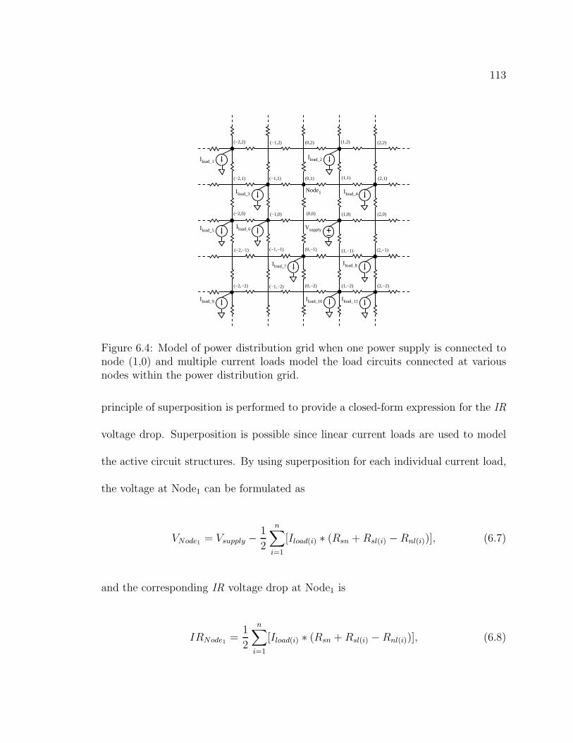
113
Vsupply
I load_1I load_2
I load_3 I load_4
I load_5I load_6
I load_7I load_8
I load_9 I load_11I load_10
Node1
(2,2)(1,2)
(2,1)(1,1)
(2,0)(1,0)
(2,−1)(1,−1)
(2,−2)(1,−2)
(0,2)
(0,1)
(0,0)
(0,−1)
(0,−2)
(−1,2)
(−1,1)
(−1,0)
(−1,−1)
(−1,−2)
(−2,2)
(−2,1)
(−2,0)
(−2,−1)
(−2,−2)
Figure 6.4: Model of power distribution grid when one power supply is connected tonode (1,0) and multiple current loads model the load circuits connected at variousnodes within the power distribution grid.
principle of superposition is performed to provide a closed-form expression for the IR
voltage drop. Superposition is possible since linear current loads are used to model
the active circuit structures. By using superposition for each individual current load,
the voltage at Node1 can be formulated as
VNode1 = Vsupply −1
2
n∑
i=1
[Iload(i) ∗ (Rsn +Rsl(i) −Rnl(i))], (6.7)
and the corresponding IR voltage drop at Node1 is
IRNode1 =1
2
n∑
i=1
[Iload(i) ∗ (Rsn +Rsl(i) −Rnl(i))], (6.8)

114
IR Drop: One Power Supply and Multiple Current Loads1. Given: Supply voltage (Vsupply), load currents (Iload(i))
Locations of voltage supply (Nsupply),current loads (Nload(i)), and Node1.
2. for each current load, Iload(i), do3. Remove all other Iload(k) where k 6=i,4. Calculate the effective resistances between
a) Nsupply and Node1, Rsn
b) Node1 and Nload(i), Rnl(i)
c) Nsupply and Nload(i), Rsl(i).5. Calculate the voltage at Nload(i), (6.1).6. Calculate the IR drop at Node1 due to Iload(i), (6.6).7. Calculate the total IR drop at Node1 by summing
all IR voltage drops due to all individual current loads, (6.8).8. Calculate the voltage at Node1, Vnode1 , (6.7).
Figure 6.5: Algorithm II. IR voltage drop at arbitrary node Node1 within a powergrid with one power supply and multiple current loads, as shown in Fig 6.4.
where n is the number of current loads, Iload(i) is the ith current load, Rsl(i) is the effec-
tive resistance between the Nsupply and the ith current load, and Rnl(i) is the effective
resistance between Node1 and the ith current load within the power grid. Pseudo-
code of the algorithm to determine the IR voltage drop at an arbitrary node when
one voltage supply and multiple current loads are connected to a power distribution
grid is provided in Fig. 6.5 (Algorithm II).
6.1.3 Multiple power supplies and one current load
In this section, the IR voltage drop at an arbitrary node within a power distri-
bution network is determined for multiple voltage sources and one current load, as
shown in Fig. 6.6a. In Section 6.1.2, superposition is used to analyze the voltage
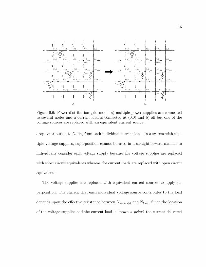
115
Node1
Vsupply_4
Node1
I load
supply_4I
supply_3I
supply_3II load
Vsupply_3
Vsupply_1
Vsupply_2
Vsupply_1
b)a)
(2,2)
(2,1)
(2,0)
(2,−1)
(2,−2)(1,−2)
(1,−1)
(1,0)
(1,1)
(1,2)(0,2)
(0,1)
(0,0)
(0,−1)
(0,−2)(−1,−2)
(−1,−1)
(−1,0)
(−1,1)
(−1,2)(−2,2)
(−2,1)
(−2,0)
(−2,−1)
(−2,−2)
(2,2)
(2,1)
(2,0)
(2,−1)
(2,−2)
(1,2)
(1,1)
(1,0)
(1,−1)
(1,−2)
(0,2)
(0,1)
(0,0)
(0,−1)
(0,−2)
(−1,2)
(−1,1)
(−1,0)
(−1,−1)
(−1,−2)
(−2,2)
(−2,1)
(−2,0)
(−2,−1)
(−2,−2)
Figure 6.6: Power distribution grid model a) multiple power supplies are connectedto several nodes and a current load is connected at (0,0) and b) all but one of thevoltage sources are replaced with an equivalent current source.
drop contribution to Node1 from each individual current load. In a system with mul-
tiple voltage supplies, superposition cannot be used in a straightforward manner to
individually consider each voltage supply because the voltage supplies are replaced
with short circuit equivalents whereas the current loads are replaced with open circuit
equivalents.
The voltage supplies are replaced with equivalent current sources to apply su-
perposition. The current that each individual voltage source contributes to the load
depends upon the effective resistance between Nsupply(i) and Nload. Since the location
of the voltage supplies and the current load is known a priori, the current delivered
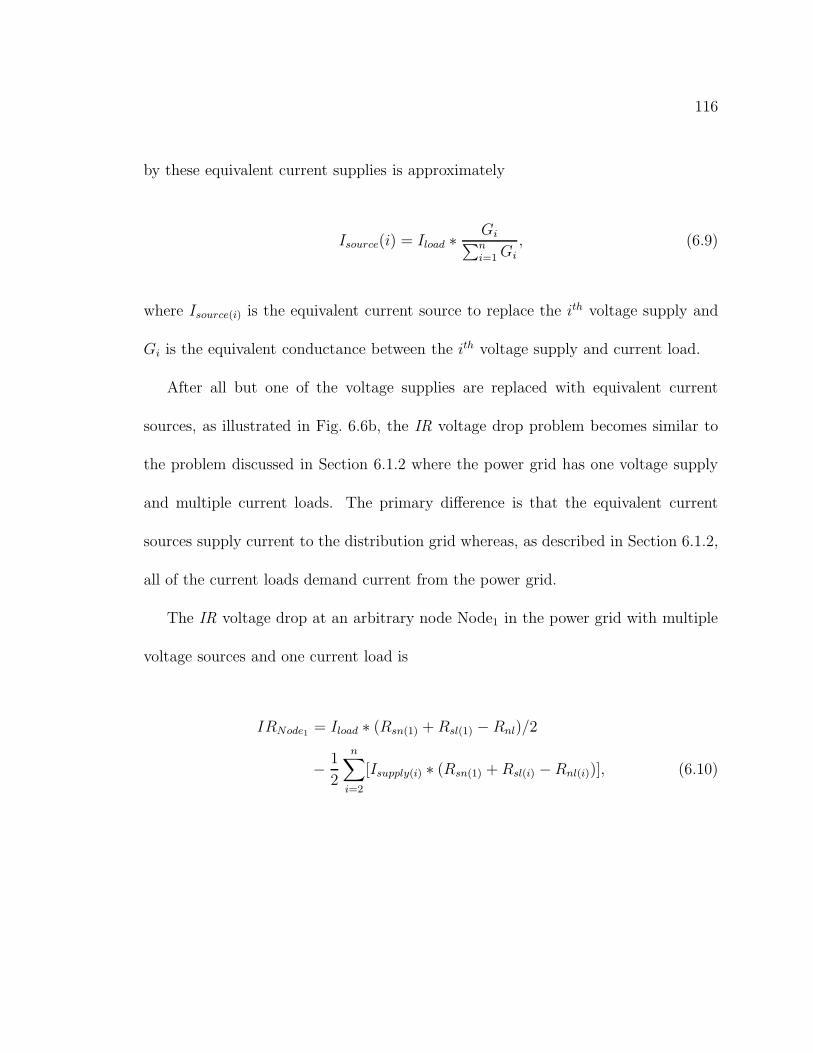
116
by these equivalent current supplies is approximately
Isource(i) = Iload ∗Gi
∑ni=1Gi
, (6.9)
where Isource(i) is the equivalent current source to replace the ith voltage supply and
Gi is the equivalent conductance between the ith voltage supply and current load.
After all but one of the voltage supplies are replaced with equivalent current
sources, as illustrated in Fig. 6.6b, the IR voltage drop problem becomes similar to
the problem discussed in Section 6.1.2 where the power grid has one voltage supply
and multiple current loads. The primary difference is that the equivalent current
sources supply current to the distribution grid whereas, as described in Section 6.1.2,
all of the current loads demand current from the power grid.
The IR voltage drop at an arbitrary node Node1 in the power grid with multiple
voltage sources and one current load is
IRNode1 = Iload ∗ (Rsn(1) +Rsl(1) − Rnl)/2
− 1
2
n∑
i=2
[Isupply(i) ∗ (Rsn(1) +Rsl(i) −Rnl(i))], (6.10)

117
and the voltage at Node1 is
VNode1 = Vsupply(1) − Iload ∗ (Rsn(1) +Rsl(1) −Rnl)/2
+1
2
n∑
i=2
[Isupply(i) ∗ (Rsn(1) +Rsl(i) −Rnl(i))]. (6.11)
Pseudo-code of the algorithm to determine the IR voltage drop at an arbitrary node
within a power grid with multiple voltage supplies and one current load is summarized
in Fig. 6.7 (Algorithm III).
6.1.4 Multiple power supplies and multiple current loads
In this section, the IR voltage drop at an arbitrary node within a power distri-
bution network is determined when multiple voltage supplies and multiple current
loads exist, as shown in Fig. 6.8a. To determine the IR voltage drop for this system,
superposition is applied in two steps. First, the current that each individual voltage
supply contributes to each individual current load is determined by removing all but
one of the current loads and applying (6.9) to determine the current contribution of
each voltage supply to each current load. After determining the individual current
contributions, the equivalent current source of a voltage supply is
Isource(i) =m∑
j=1
Isource(i,j), (6.12)
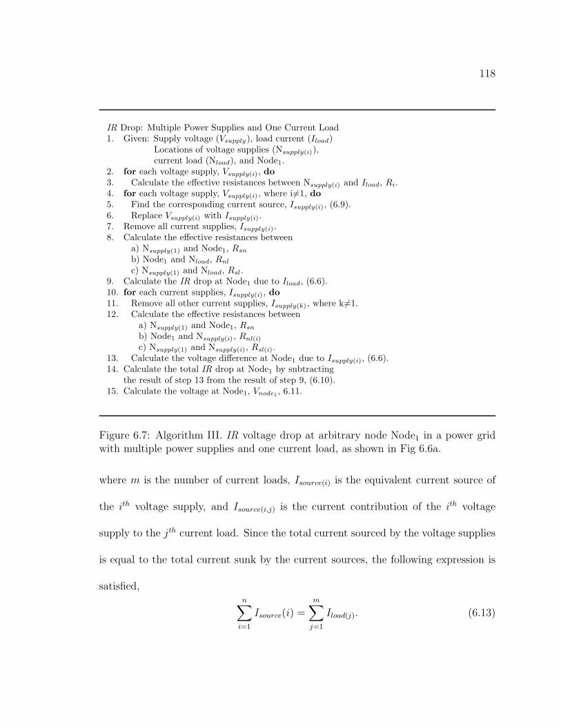
118
IR Drop: Multiple Power Supplies and One Current Load1. Given: Supply voltage (Vsupply), load current (Iload)
Locations of voltage supplies (Nsupply(i)),current load (Nload), and Node1.
2. for each voltage supply, Vsupply(i), do3. Calculate the effective resistances between Nsupply(i) and Iload, Ri.4. for each voltage supply, Vsupply(i), where i 6=1, do5. Find the corresponding current source, Isupply(i), (6.9).6. Replace Vsupply(i) with Isupply(i).7. Remove all current supplies, Isupply(i).8. Calculate the effective resistances between
a) Nsupply(1) and Node1, Rsn
b) Node1 and Nload, Rnl
c) Nsupply(1) and Nload, Rsl.9. Calculate the IR drop at Node1 due to Iload, (6.6).10. for each current supplies, Isupply(i), do11. Remove all other current supplies, Isupply(k) , where k 6=1.12. Calculate the effective resistances between
a) Nsupply(1) and Node1, Rsn
b) Node1 and Nsupply(i), Rnl(i)
c) Nsupply(1) and Nsupply(i), Rsl(i).13. Calculate the voltage difference at Node1 due to Isupply(i), (6.6).14. Calculate the total IR drop at Node1 by subtracting
the result of step 13 from the result of step 9, (6.10).15. Calculate the voltage at Node1, Vnode1 , 6.11.
Figure 6.7: Algorithm III. IR voltage drop at arbitrary node Node1 in a power gridwith multiple power supplies and one current load, as shown in Fig 6.6a.
where m is the number of current loads, Isource(i) is the equivalent current source of
the ith voltage supply, and Isource(i,j) is the current contribution of the ith voltage
supply to the jth current load. Since the total current sourced by the voltage supplies
is equal to the total current sunk by the current sources, the following expression is
satisfied,n∑
i=1
Isource(i) =
m∑
j=1
Iload(j). (6.13)
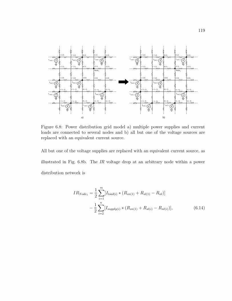
119
Node1 Node1
supply_2II load_1
I load_4
I load_3
supply_4II load_5
supply_3I
I load_2
Vsupply_1Vsupply_2I load_1
I load_4
Vsupply_4
I load_3
I load_5
Vsupply_3
I load_2
Vsupply_1
b)a)
(2,2)
(2,1)
(2,0)
(2,−1)
(2,−2)
(1,2)
(1,1)
(1,0)
(1,−1)
(1,−2)
(0,2)
(0,1)
(0,0)
(0,−1)
(0,−2)
(−1,2)
(−1,1)
(−1,0)
(−1,−1)
(−1,−2)
(−2,2)
(−2,1)
(−2,0)
(−2,−1)
(−2,−2)
(2,2)
(2,1)
(2,0)
(2,−1)
(2,−2)(1,−2)
(1,2)
(1,1)
(1,0)
(1,−1)
(0,2)
(0,1)
(0,0)
(0,−1)
(0,−2)
(−1,2)
(−1,1)
(−1,0)
(−1,−1)
(−1,−2)
(−2,2)
(−2,1)
(−2,0)
(−2,−1)
(−2,−2)
Figure 6.8: Power distribution grid model a) multiple power supplies and currentloads are connected to several nodes and b) all but one of the voltage sources arereplaced with an equivalent current source.
All but one of the voltage supplies are replaced with an equivalent current source, as
illustrated in Fig. 6.8b. The IR voltage drop at an arbitrary node within a power
distribution network is
IRNode1 =1
2
m∑
i=1
[Iload(i) ∗ (Rsn(1) +Rsl(1) −Rnl)]
− 1
2
n∑
i=2
[Isupply(i) ∗ (Rsn(1) +Rsl(i) −Rnl(i))], (6.14)

120
and the corresponding voltage at Node1 is
VNode1 = Vsupply(1)
− 1
2
m∑
i=1
[Iload(i) ∗ (Rsn(1) +Rsl(1) − Rnl)]
+1
2
n∑
i=2
[Isupply(i) ∗ (Rsn(1) +Rsl(i) − Rnl(i))], (6.15)
where m is the number of current loads and n is the number of voltage supplies.
Pseudo-code of the algorithm to determine the IR voltage drop at an arbitrary node
for multiple voltage supplies and current loads is provided in Fig. 6.9 (Algorithm IV).
6.2 Locality in Power Grid Analysis
Practical power grids in high performance integrated circuits can be treated as
locally uniform, globally non-uniform resistive meshes. To apply these algorithms to
the analysis of practical power grids, the principle of spatial locality [108,171,175–177]
is applied. This principle for a resistive power grid is described in Section 6.2.1.
The effect of utilizing spatial locality on the power grid analysis process is explained
in Section 6.2.2. In Section 6.2.3, the principle of spatial locality is exploited and
integrated into this power grid analysis method. The advantages of utilizing spatial
locality in the power grid analysis process are also explored. An error correction
technique is introduced in Section 6.2.4.

121
IR Drop: Multiple Power Supplies and Multiple Current Loads1. Given: Supply voltage (Vsupply), load currents (Iload(j))
Locations of voltage supplies (Nsupply(i)),current loads (Nload(j)), and Node1.
2. for each voltage supply, Vsupply(i), do3. for each current load, Iload(j), do4. Calculate the effective resistances between
Nsupply(i) and Iload(j), R(i,j).5. for each voltage supply, Vsupply(i), where i 6=1, do6. for each current load, Iload(j), do7. Find the corresponding current, Isupply(i,j) , (6.9).8. Sum up Isupply(i,j) for all j to calculate Isupply(i), (6.12).9. Replace Vsupply(i) with Isupply(i).10. for each current load, Iload(j), do11. Remove all current supplies, Isupply(i) .12. Calculate the effective resistances between
a) Nsupply(1) and Node1, Rsn
b) Node1 and Nload(j), Rnl(j)
c) Nsupply(1) and Nload(j), Rsl(1,j).13. Calculate the IR drop at Node1 due to all Iload(j), (6.6).14. for each current supply, Isupply(i) , do15. Remove all other current supplies, Isupply(k) , where k 6=1.16. Remove all current loads, Iload(j).17. Calculate the effective resistances between
a) Nsupply(1) and Node1, Rsn
b) Node1 and Nsupply(i), Rnl(i)
c) Nsupply(1) and Nsupply(i), Rsl(i).18. Calculate the voltage difference at Node1 due to Isupply(i), (6.6).19. Calculate the total IR drop at Node1 by subtracting
the result of step 18 from the result of step 13, (6.14).20. Calculate the voltage at Node1, Vnode1 , (6.15).
Figure 6.9: Algorithm IV. IR voltage drop at an arbitrary node Node1 within a powergrid with multiple power supplies and current loads, as shown in Fig 6.8a.
6.2.1 Principle of spatial locality in a power grid
Flip-chip packages are widely used in high performance integrated circuits, increas-
ing the number of voltage supply connections to the integrated circuit. Controlled
collapse chip connect (C4) bumps connect the integrated circuit to external circuitry

122
from the top side of the wafer using solder bumps. A large number of power supply
connections are therefore provided to the power grid via these C4 bumps. Most of the
current to the load devices is provided from those power supply connections in close
proximity due to the smaller effective impedance. This phenomenon can be explained
using the principle of spatial locality in a power grid [108, 171, 175, 177].
A power grid for a flip-chip package with C4 connections is illustrated in Fig. 6.10.
To exemplify the principle of spatial locality in a power grid, two current loads are
connected to the power grid, as depicted in Fig. 6.10, to analyze the current contri-
butions from each supply connection. With only one current load L1 connected to
the power grid, the current contributed from each of the C4 connections to L1 is as
illustrated in Fig. 6.11. Most of the current is provided by the close power supplies.
The current contribution of a supply connection decreases significantly with distance.
The current contribution from most of the supply connections within the third ring
is less than 1% of the total load current. The current contribution from each supply
connection is also analyzed with only the current load L2 connected to the power
grid. More than 40% of the total current is provided by the closest power supply
connection, V21. The current contribution of all of the connections is illustrated in
Fig. 6.12. Most of the power supply connections within the third ring contribute less
than 1% of the current to the load. When the load circuit is close to the boundary
of the power supply ring, the current provided by some power supply connections
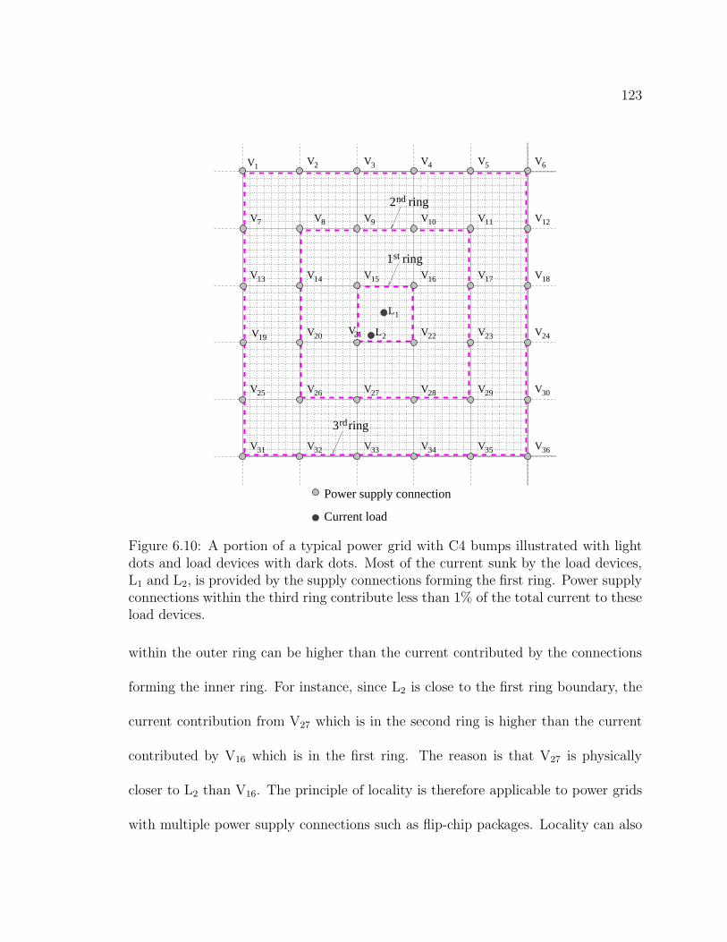
123
1 ring
2 ring
3 ring
Power supply connection
Current load
st
nd
rd
L1
L2
V1V2 V3 V4 V5 V6
V7 V8 V9 V10 V11 V12
V13 V14 V15 V16 V17 V18
V19V20 V22 V23 V24
V25 V26 V27 V28 V29 V30
V31 V32 V33 V34 V35 V36
V21
Figure 6.10: A portion of a typical power grid with C4 bumps illustrated with lightdots and load devices with dark dots. Most of the current sunk by the load devices,L1 and L2, is provided by the supply connections forming the first ring. Power supplyconnections within the third ring contribute less than 1% of the total current to theseload devices.
within the outer ring can be higher than the current contributed by the connections
forming the inner ring. For instance, since L2 is close to the first ring boundary, the
current contribution from V27 which is in the second ring is higher than the current
contributed by V16 which is in the first ring. The reason is that V27 is physically
closer to L2 than V16. The principle of locality is therefore applicable to power grids
with multiple power supply connections such as flip-chip packages. Locality can also
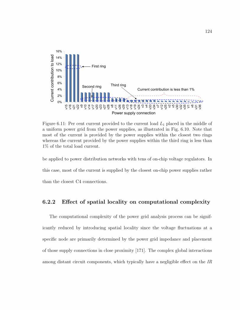
124
v32 7.38 v32 0.7 %
v13 6.98 v13 0.7 %
v25 6.58 v25 0.7 %
v35 4.89 v35 0.5 %
v11 4.59 v11 0.5 %
v31 4.11 v31 0.4 %
v24 3.99 v24 0.4 %
v7 3.42 v7 0.3 %
v30 3.24 v30 0.3 %
v18 3.21 v18 0.3 %
v3 3.11 v3 0.3 %
v4 2.73 v4 0.3 %
v36 2.51 v36 0.3 %
v2 2.35 v2 0.2 %
v12 1.78 v12 0.2 %
V1 1.72 v1 0.2 %
v5 1.65 v5 0.2 %
v6 1.05 v6 0.1 %
Current contribution is less than 1%
0%
2%
4%
6%
8%
10%
12%
14%
16%
v1
5
v1
6
v2
1
v2
2
v9
v1
0
v1
4
v1
7
v2
0
v2
3
v2
7
v2
8
v8
v1
1
v2
6
v2
9
v1
3
v1
8
v1
9
v2
4
v3
v4
v3
3
v3
4
v7
v1
2
v2
5
v2
v5
v3
0
v3
2
v3
5
V1
v6
v3
1
v3
6
Power supply connection
Curr
ent
contr
ibution t
o load
Second ring
First ring
Third ring
Figure 6.11: Per cent current provided to the current load L1 placed in the middle ofa uniform power grid from the power supplies, as illustrated in Fig. 6.10. Note thatmost of the current is provided by the power supplies within the closest two ringswhereas the current provided by the power supplies within the third ring is less than1% of the total load current.
be applied to power distribution networks with tens of on-chip voltage regulators. In
this case, most of the current is supplied by the closest on-chip power supplies rather
than the closest C4 connections.
6.2.2 Effect of spatial locality on computational complexity
The computational complexity of the power grid analysis process can be signif-
icantly reduced by introducing spatial locality since the voltage fluctuations at a
specific node are primarily determined by the power grid impedance and placement
of those supply connections in close proximity [171]. The complex global interactions
among distant circuit components, which typically have a negligible effect on the IR
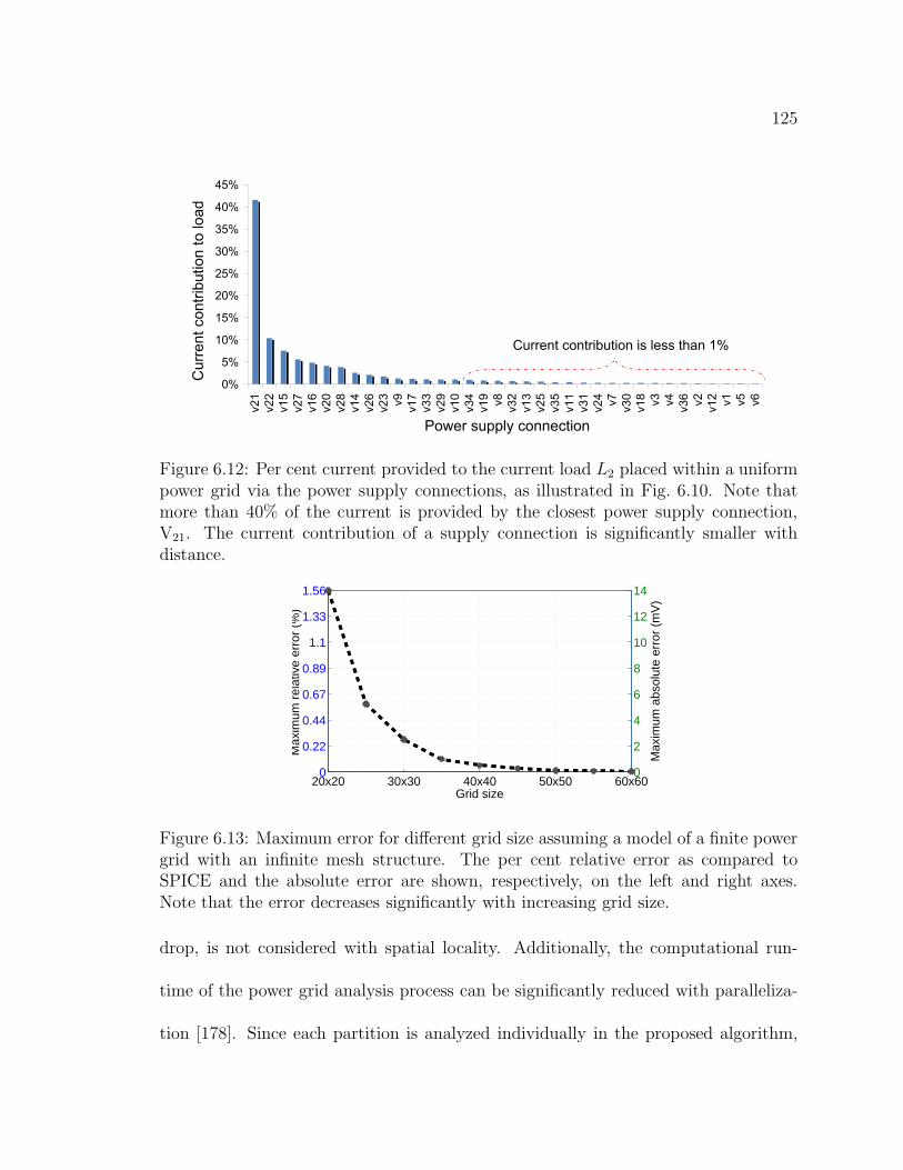
125
v21 415.8 v21 41.6 %
v22 104.44 v22 10.4 %
v15 76 v15 7.6 %
v27 56.7 v27 5.7 %
v16 48.8 v16 4.9 %
v20 42.3 v20 4.2 %
v28 39.55 v28 4.0 %
v14 26.34 v14 2.6 %
v26 21.81 v26 2.2 %
v23 17.32 v23 1.7 %
v9 13.4 v9 1.3 %
v17 12.24 v17 1.2 %
v33 11.62 v33 1.2 %
v29 11.03 v29 1.1 %
v10 10.94 v10 1.1 %
v34 9.87 v34 1.0 %
v19 8.96 v19 0.9 %
v8 7.73 v8 0.8 %
v32 7.38 v32 0.7 %
Current contribution is less than 1%
0%
5%
10%
15%
20%
25%
30%
35%
40%
45%
v2
1
v2
2
v1
5
v2
7
v1
6
v2
0
v2
8
v1
4
v2
6
v2
3
v9
v1
7
v3
3
v2
9
v1
0
v3
4
v1
9
v8
v3
2
v1
3
v2
5
v3
5
v1
1
v3
1
v2
4
v7
v3
0
v1
8
v3
v4
v3
6
v2
v1
2
v1
v5
v6
Power supply connection
Curr
ent
contr
ibution t
o load
Curr
ent
contr
ibution t
o load
Figure 6.12: Per cent current provided to the current load L2 placed within a uniformpower grid via the power supply connections, as illustrated in Fig. 6.10. Note thatmore than 40% of the current is provided by the closest power supply connection,V21. The current contribution of a supply connection is significantly smaller withdistance.
0
0.22
0.44
0.67
0.89
1.1
1.33
1.56
Max
imum
rel
ativ
e er
ror
(%)
20x20 30x30 40x40 50x50 60x600
2
4
6
8
10
12
14
Max
imum
abs
olut
e er
ror
(mV
)
Grid size
Figure 6.13: Maximum error for different grid size assuming a model of a finite powergrid with an infinite mesh structure. The per cent relative error as compared toSPICE and the absolute error are shown, respectively, on the left and right axes.Note that the error decreases significantly with increasing grid size.
drop, is not considered with spatial locality. Additionally, the computational run-
time of the power grid analysis process can be significantly reduced with paralleliza-
tion [178]. Since each partition is analyzed individually in the proposed algorithm,

126
A
DC
B B
D
A
C
Overlapping boundry
Power supply connection Locality window
Analysis partition
Figure 6.14: Power grid divided into smaller partitions. Each partition consists of ananalysis partition and overlapping boundary.
parallelization of the proposed algorithm is straightforward.
6.2.3 Exploiting spatial locality in the proposed method
An infinite grid is assumed in these algorithms when using the effective resistance
model proposed in 5 to determine the effective resistance of a finite power grid. This
assumption introduces an approximation error to the proposed power grid analysis
process when evaluating small power grids. When the size of the power grid increases,
the introduced error converges to zero. The maximum error for various grid sizes is
illustrated in Fig. 6.13. When the grid size is larger than 30×30, the error is less than
0.5% of the supply voltage. Modern power grids can contain more than a million
nodes. The size of these grids typically exceed 1000×1000, making the approximation

127
error effectively zero.
A power grid is divided into smaller partitions [171, 177] to exploit the principle
of spatial locality. Each partition is analyzed individually and a complete solution is
obtained by combining the results of each partition. The ideal solution is obtained
with only one partition (i.e., no partitioning), thereby considering all of the inter-
actions among each power supply and load circuit. This approach suffers from long
computational time. The fastest solution is obtained when the power grid is divided
into the smallest possible partitions. This analysis, however, can introduce significant
error. A tradeoff in partition size therefore exists between computational complexity
and accuracy.
For each partition, the error is smallest in the middle of the partition and in-
creases towards the boundaries. A partitioning approach divides the power grid into
several overlapping windows where only the middle of each window is analyzed. The
boundaries of each partition overlap with the adjacent partitions. This method of
overlapping windows has been shown to be effective in industrial power grids to ac-
celerate the power grid analysis process [171]. Some redundancy is introduced during
the analysis process which significantly reduces the error from application of spatial
locality. This partitioning approach is illustrated in Fig. 6.14 where a flip-chip power
grid with several C4 connections is partitioned into four overlapping windows. Each
window consists of an analysis partition and an overlapping boundary. The size of
128
each partition and overlapping boundary is chosen sufficiently large to minimize the
error caused by the partitioning process. A tradeoff therefore also exists between
computational complexity and induced error in the size of the overlapping boundary.
When the size of the overlapping boundary is sufficiently large, the effect of the adja-
cent power grid partition is minimized. Alternatively, the computational complexity
of the analysis process decreases when the size of the overlapping boundary is small.
In this chapter, the size of each partition and the overlapping boundary is maintained
larger than 100×100 and 20, respectively, making the approximation error less than
0.1%. The partitioning approach also considers the locally uniform, globally non-
uniform nature of the power grid. Each partition is treated as a uniform power grid.
Different partitions can exhibit different impedance characteristics.
6.2.4 Error correction windows
Several error reduction techniques can be implemented within this algorithm. One
technique is the use of error correction windows, as illustrated in Fig. 6.15, where
the supply connections, load circuits, error correction window, and analysis window
are shown, respectively, with a light dot, dark dot, light gray box, and green box.
Since the voltage at each supply connection is known a priori, the induced error
at a supply connection is the difference between the ideal supply voltage and the
voltage determined from this algorithm. This error is primarily introduced when
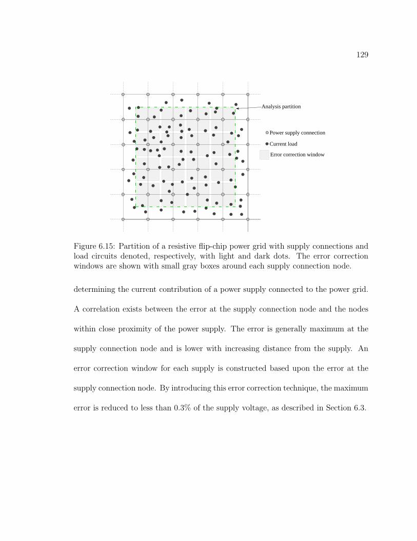
129
Power supply connection
Current load
Error correction window
Analysis partition
Figure 6.15: Partition of a resistive flip-chip power grid with supply connections andload circuits denoted, respectively, with light and dark dots. The error correctionwindows are shown with small gray boxes around each supply connection node.
determining the current contribution of a power supply connected to the power grid.
A correlation exists between the error at the supply connection node and the nodes
within close proximity of the power supply. The error is generally maximum at the
supply connection node and is lower with increasing distance from the supply. An
error correction window for each supply is constructed based upon the error at the
supply connection node. By introducing this error correction technique, the maximum
error is reduced to less than 0.3% of the supply voltage, as described in Section 6.3.
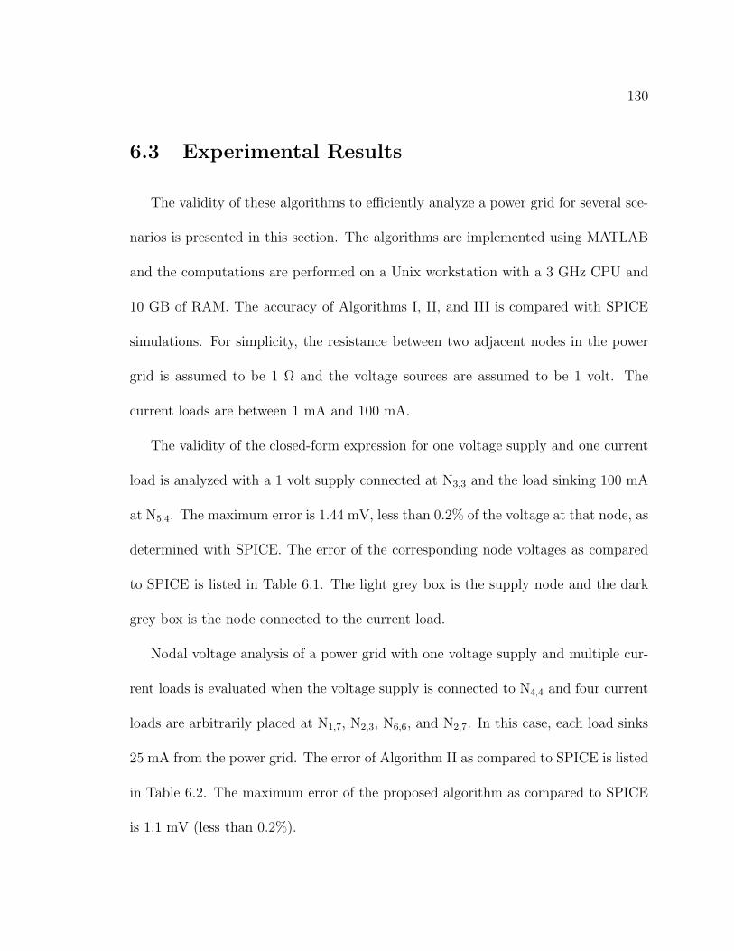
130
6.3 Experimental Results
The validity of these algorithms to efficiently analyze a power grid for several sce-
narios is presented in this section. The algorithms are implemented using MATLAB
and the computations are performed on a Unix workstation with a 3 GHz CPU and
10 GB of RAM. The accuracy of Algorithms I, II, and III is compared with SPICE
simulations. For simplicity, the resistance between two adjacent nodes in the power
grid is assumed to be 1 Ω and the voltage sources are assumed to be 1 volt. The
current loads are between 1 mA and 100 mA.
The validity of the closed-form expression for one voltage supply and one current
load is analyzed with a 1 volt supply connected at N3,3 and the load sinking 100 mA
at N5,4. The maximum error is 1.44 mV, less than 0.2% of the voltage at that node, as
determined with SPICE. The error of the corresponding node voltages as compared
to SPICE is listed in Table 6.1. The light grey box is the supply node and the dark
grey box is the node connected to the current load.
Nodal voltage analysis of a power grid with one voltage supply and multiple cur-
rent loads is evaluated when the voltage supply is connected to N4,4 and four current
loads are arbitrarily placed at N1,7, N2,3, N6,6, and N2,7. In this case, each load sinks
25 mA from the power grid. The error of Algorithm II as compared to SPICE is listed
in Table 6.2. The maximum error of the proposed algorithm as compared to SPICE
is 1.1 mV (less than 0.2%).

131
Table 6.1: Error of Algorithm I as compared to SPICE. The voltage supply is con-nected at N3,3 (light gray) and the load device is connected at N5,4 (dark gray). Themaximum error is less than 0.2% of the supply voltage.
1 2 3 4 5 6 7 8
1 -0.12 -0.05 0.46 -0.27 -0.49 -0.26 -0.125 -0.152 -0.09 -0.55 0.79 0.152 -0.68 -0.37 -0.554 -0.143 0.33 0.62 0 1.13 -0.52 0.52 0 -0.264 -0.31 -0.83 0.21 -1.44 -0.31 -0.93 -0.64 -0.415 -0.25 -0.27 0.37 0.24 -1.10 0.24 -0.22 -0.386 -0.18 -0.04 0.18 -0.04 -0.77 -0.25 -0.18 -0.307 -0.13 -0.01 0 -0.23 -0.50 -0.36 -0.28 -0.308 -0.14 -0.04 -0.08 -0.27 -0.32 -0.34 -0.34 -0.34
Table 6.2: Error of Algorithm II as compared to SPICE. The voltage supply is con-nected at N4,4 (light gray) and the load devices are connected at N1,7, N2,3, N6,6, andN2,7 (dark gray). The maximum error is less than 0.2% of the supply voltage.
1 2 3 4 5 6 7 8
1 -0.17 -0.24 -0.06 0.07 -0.16 -0.38 -0.19 -0.302 0.01 -0.40 -0.06 0.32 -0.20 -0.14 -0.36 -0.033 -0.23 -0.25 -0.80 0.60 -0.64 -0.25 -0.18 -0.024 0.28 0.11 0.76 0 0.69 0.18 0.05 0.025 0.01 -0.40 -0.64 0.75 -0.50 -0.42 -0.06 -0.046 0 -0.49 -0.08 0.28 -0.39 -0.31 -0.36 -0.237 -0.40 -0.25 -0.32 0.12 -0.04 -0.45 -0.07 -0.138 -0.05 -0.35 1.11 0.08 -0.02 -0.29 -0.16 -0.17
The validity of Algorithm III is analyzed with three voltage supplies and a current
load connected arbitrarily to the power grid. The current load sinks 100 mA current
and the voltage supplies are 1 volt. The maximum voltage drop is less than 100 mV.
The error of Algorithm III as compared to SPICE is tabulated in Table 6.3. The
maximum error is 1.41 mV which is smaller than 0.2% of the voltage, as determined
with SPICE.
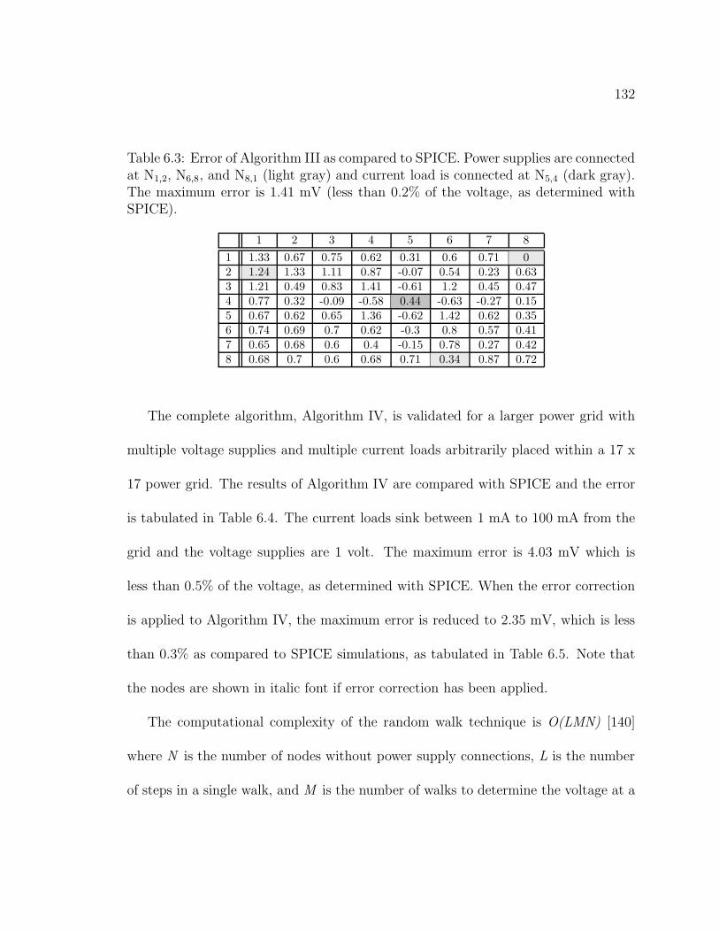
132
Table 6.3: Error of Algorithm III as compared to SPICE. Power supplies are connectedat N1,2, N6,8, and N8,1 (light gray) and current load is connected at N5,4 (dark gray).The maximum error is 1.41 mV (less than 0.2% of the voltage, as determined withSPICE).
1 2 3 4 5 6 7 8
1 1.33 0.67 0.75 0.62 0.31 0.6 0.71 02 1.24 1.33 1.11 0.87 -0.07 0.54 0.23 0.633 1.21 0.49 0.83 1.41 -0.61 1.2 0.45 0.474 0.77 0.32 -0.09 -0.58 0.44 -0.63 -0.27 0.155 0.67 0.62 0.65 1.36 -0.62 1.42 0.62 0.356 0.74 0.69 0.7 0.62 -0.3 0.8 0.57 0.417 0.65 0.68 0.6 0.4 -0.15 0.78 0.27 0.428 0.68 0.7 0.6 0.68 0.71 0.34 0.87 0.72
The complete algorithm, Algorithm IV, is validated for a larger power grid with
multiple voltage supplies and multiple current loads arbitrarily placed within a 17 x
17 power grid. The results of Algorithm IV are compared with SPICE and the error
is tabulated in Table 6.4. The current loads sink between 1 mA to 100 mA from the
grid and the voltage supplies are 1 volt. The maximum error is 4.03 mV which is
less than 0.5% of the voltage, as determined with SPICE. When the error correction
is applied to Algorithm IV, the maximum error is reduced to 2.35 mV, which is less
than 0.3% as compared to SPICE simulations, as tabulated in Table 6.5. Note that
the nodes are shown in italic font if error correction has been applied.
The computational complexity of the random walk technique is O(LMN) [140]
where N is the number of nodes without power supply connections, L is the number
of steps in a single walk, and M is the number of walks to determine the voltage at a

133
Table 6.4: Error of Algorithm IV as compared to SPICE. Power supplies are connected at the corners (light gray)and current loads are connected at various nodes (dark gray). The maximum error is 4.03 mV (less than 0.5%of the voltage, as determined with SPICE). Error correction is not used in this example and the maximum erroroccurs at the supply connection.
1 2 3 4 5 6 7 8 9 10 11 12 13 14 15 16 17
1 0 0.36 0.10 -0.25 -0.32 -0.43 -0.57 -0.53 -0.28 0.07 0.39 0.87 1.1 1.71 2.26 3.06 4.032 0.4 -0.52 -0.4 -0.29 -0.45 -0.67 -0.93 -1.15 -0.68 -0.18 0.22 0.65 1.08 1.43 1.76 1.87 3.33 0.18 -0.27 -0.39 -0.45 -0.58 -0.85 -1.31 -2.35 -1 -0.32 0.19 0.62 0.91 1.28 1.56 1.94 2.54 -0.12 -0.24 -0.36 -0.44 -0.49 -0.73 -1.09 -1.17 -0.64 -0.2 0.24 0.56 0.84 1.22 1.55 1.75 2.15 -0.2 -0.26 -0.31 -0.36 -0.42 -0.46 -0.93 -0.56 -0.25 0.01 0.28 0.55 0.89 1.19 1.42 1.65 1.836 -0.28 -0.3 -0.38 -0.38 -0.31 -0.07 -0.9 -0.01 -0.07 0.09 0.23 0.58 0.89 1.12 1.37 1.48 1.667 -0.33 -0.29 -0.31 -0.44 -0.56 -0.83 -0.27 -0.54 -0.17 0.14 0.2 0.69 0.93 1.12 1.25 1.44 1.618 -0.34 -0.3 -0.34 -0.22 -0.15 -0.11 -0.28 0.43 0.2 0.57 0.18 0.96 0.91 1.06 1.25 1.43 1.489 -0.36 -0.33 -0.35 -0.23 0.18 -0.4 0.03 0.11 -0.16 0.12 0.59 0.39 0.67 0.99 1.18 1.35 1.5210 -0.46 -0.47 -0.4 -0.48 -0.54 -0.2 -0.46 0.15 -0.06 0.99 0.3 1.05 1 1.15 1.19 1.38 1.5111 -0.44 -0.48 -0.36 -0.24 0.07 -0.62 0.05 -0.11 0.37 0.16 0.21 0.75 1.02 1.25 1.28 1.55 1.5612 -0.48 -0.5 -0.35 -0.3 -0.14 -0.36 0.17 0.6 0.13 0.81 0.58 0.84 1.05 1.18 1.37 1.44 1.6713 -0.55 -0.48 -0.48 -0.37 -0.27 -0.18 0.1 0.3 0.26 0.7 0.68 1.02 1.14 1.38 1.39 1.74 1.8414 -0.6 -0.65 -0.64 -0.53 -0.24 -0.12 0.12 0.2 0.28 0.51 0.87 0.97 1.15 1.37 1.55 1.8 2.0615 -0.7 -0.93 -0.77 -0.55 -0.25 -0.09 0.09 0.24 0.44 0.68 0.82 1.09 1.29 1.44 1.66 1.91 2.3916 -0.95 -1.58 -0.94 -0.56 -0.32 -0.11 0.03 0.25 0.46 0.72 0.88 1.12 1.35 1.57 1.83 1.89 3.0417 -2.49 -0.84 -0.46 -0.51 -0.16 -0.03 0.16 0.3 0.52 0.65 0.84 1.14 1.37 1.73 2.21 2.92 3.47
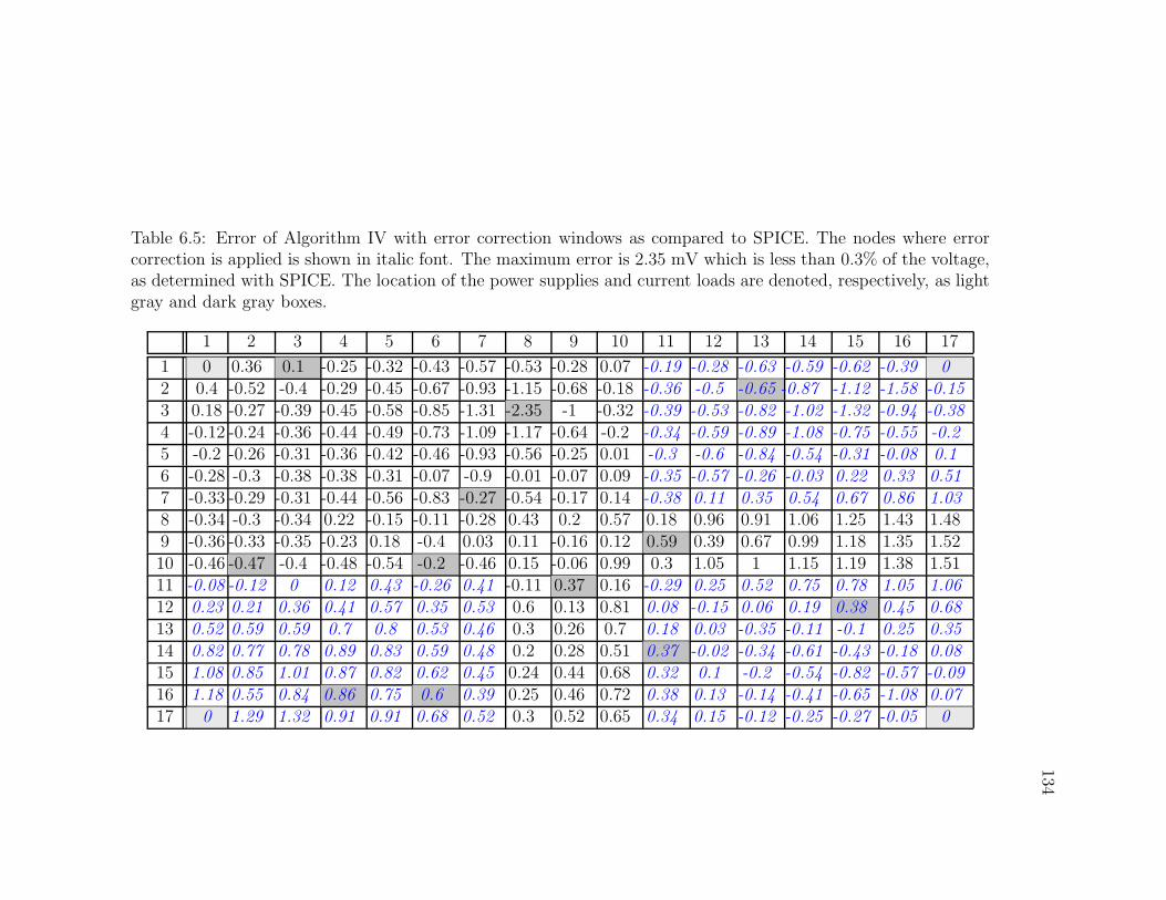
134
Table 6.5: Error of Algorithm IV with error correction windows as compared to SPICE. The nodes where errorcorrection is applied is shown in italic font. The maximum error is 2.35 mV which is less than 0.3% of the voltage,as determined with SPICE. The location of the power supplies and current loads are denoted, respectively, as lightgray and dark gray boxes.
1 2 3 4 5 6 7 8 9 10 11 12 13 14 15 16 17
1 0 0.36 0.1 -0.25 -0.32 -0.43 -0.57 -0.53 -0.28 0.07 -0.19 -0.28 -0.63 -0.59 -0.62 -0.39 02 0.4 -0.52 -0.4 -0.29 -0.45 -0.67 -0.93 -1.15 -0.68 -0.18 -0.36 -0.5 -0.65 -0.87 -1.12 -1.58 -0.153 0.18 -0.27 -0.39 -0.45 -0.58 -0.85 -1.31 -2.35 -1 -0.32 -0.39 -0.53 -0.82 -1.02 -1.32 -0.94 -0.384 -0.12 -0.24 -0.36 -0.44 -0.49 -0.73 -1.09 -1.17 -0.64 -0.2 -0.34 -0.59 -0.89 -1.08 -0.75 -0.55 -0.25 -0.2 -0.26 -0.31 -0.36 -0.42 -0.46 -0.93 -0.56 -0.25 0.01 -0.3 -0.6 -0.84 -0.54 -0.31 -0.08 0.16 -0.28 -0.3 -0.38 -0.38 -0.31 -0.07 -0.9 -0.01 -0.07 0.09 -0.35 -0.57 -0.26 -0.03 0.22 0.33 0.517 -0.33 -0.29 -0.31 -0.44 -0.56 -0.83 -0.27 -0.54 -0.17 0.14 -0.38 0.11 0.35 0.54 0.67 0.86 1.038 -0.34 -0.3 -0.34 0.22 -0.15 -0.11 -0.28 0.43 0.2 0.57 0.18 0.96 0.91 1.06 1.25 1.43 1.489 -0.36 -0.33 -0.35 -0.23 0.18 -0.4 0.03 0.11 -0.16 0.12 0.59 0.39 0.67 0.99 1.18 1.35 1.5210 -0.46 -0.47 -0.4 -0.48 -0.54 -0.2 -0.46 0.15 -0.06 0.99 0.3 1.05 1 1.15 1.19 1.38 1.5111 -0.08 -0.12 0 0.12 0.43 -0.26 0.41 -0.11 0.37 0.16 -0.29 0.25 0.52 0.75 0.78 1.05 1.0612 0.23 0.21 0.36 0.41 0.57 0.35 0.53 0.6 0.13 0.81 0.08 -0.15 0.06 0.19 0.38 0.45 0.6813 0.52 0.59 0.59 0.7 0.8 0.53 0.46 0.3 0.26 0.7 0.18 0.03 -0.35 -0.11 -0.1 0.25 0.3514 0.82 0.77 0.78 0.89 0.83 0.59 0.48 0.2 0.28 0.51 0.37 -0.02 -0.34 -0.61 -0.43 -0.18 0.0815 1.08 0.85 1.01 0.87 0.82 0.62 0.45 0.24 0.44 0.68 0.32 0.1 -0.2 -0.54 -0.82 -0.57 -0.0916 1.18 0.55 0.84 0.86 0.75 0.6 0.39 0.25 0.46 0.72 0.38 0.13 -0.14 -0.41 -0.65 -1.08 0.0717 0 1.29 1.32 0.91 0.91 0.68 0.52 0.3 0.52 0.65 0.34 0.15 -0.12 -0.25 -0.27 -0.05 0

135
node. The random walk method is faster for flip chip power grids as compared to wire-
bonded power grids or power grids with a limited number of on-chip power supplies
since M is significantly larger. The computational complexity of the random walk
method can, however, be decreased with hierarchical methods [140,179], although the
property of locality is sacrificed.
Alternatively, the computational complexity of the proposed method is linear
with the size of the power grid. Since no iterations are required (i.e., L = 1) and
the voltage is determined with closed-form expressions (i.e., M = 1), the compu-
tational complexity is O(N). Although converting the voltage sources to equivalent
current sources also requires computational effort, this computational procedure is
a one time process, and the additional computational complexity is negligible. The
computational complexity also does not depend on the type of power grid (e.g., the
same computational complexity for flip chip power grids, wire-bonded power grids,
and power grids with on-chip power supplies).
To compare the computational runtime of this method with previously proposed
techniques, five differently sized circuits with evenly distributed C4 bumps 25 nodes
from each other are considered. The runtime of the proposed algorithm is compared
with the random walk method in [180] and the second order iterative method in [181],
as shown in Table 6.6. The partition size for all of the circuits when utilizing locality
is larger than 100×100 to maintain an approximation error of less than 0.1%. The
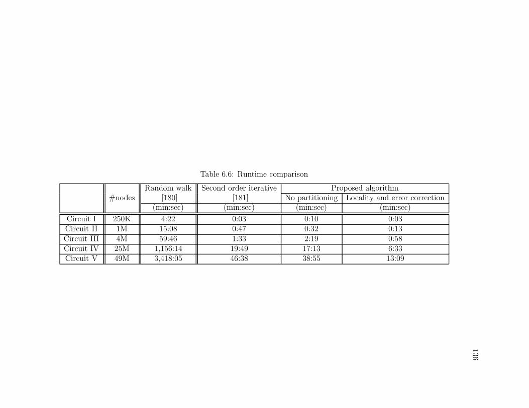
136
Table 6.6: Runtime comparison
#nodesRandom walk Second order iterative Proposed algorithm
[180] [181] No partitioning Locality and error correction(min:sec) (min:sec) (min:sec) (min:sec)
Circuit I 250K 4:22 0:03 0:10 0:03Circuit II 1M 15:08 0:47 0:32 0:13Circuit III 4M 59:46 1:33 2:19 0:58Circuit IV 25M 1,156:14 19:49 17:13 6:33Circuit V 49M 3,418:05 46:38 38:55 13:09
137
random walk method is applied for 20,000 iterations on each circuit to accurately de-
termine the node voltages. The number of iterations of the random walk and second
order iterative methods is chosen to maintain a maximum error of less than 5 mV as
compared to the results with 20,000 iterations. The error of the proposed method is
also less than 5 mV for each circuit. This method with locality is over 60 and two
times faster as compared to the random walk and second order iterative methods,
respectively, for power grids smaller than five million nodes. For circuit sizes greater
than 25 million nodes (e.g., Circuits IV and V listed in Table 6.6), the proposed
algorithm with locality is over 175 times and three times faster as compared to the
random walk and second order iterative methods, respectively. The runtime of the
random walk method depends strongly upon the number of power supply connections.
When the number of power supply connections decreases, the computational runtime
of the random walk method dramatically increases. Alternatively, the computational
runtime of the proposed method is lower with fewer number of power supply connec-
tions.
6.4 Summary
Closed-form expressions and related algorithms for fast IR voltage drop analysis
are provided in this chapter. The physical distance between the circuit components
and the principal of spatial locality are exploited. Significant computational time is

138
required to analyze power grids when the size of the grid is large. Efficient algorithms
are therefore required to reduce the computational runtime of the power grid analysis
process. A novel algorithm is described for analyzing locally uniform, globally non-
uniform power grids with non-uniform current loads and non-uniform voltage supplies.
The power grid impedance characteristics and the euclidean distance between the cir-
cuit components are utilized to develop the closed-form expressions. Local analyses
of power distribution networks can be performed with the proposed algorithm. Par-
allel computation of the IR drop analysis algorithm is also possible. A novel error
correction technique exploiting the principle of spatial locality is described to improve
the accuracy. The proposed power grid analysis algorithm is more computationally
efficient than existing IR drop analysis techniques since no iterations are required.

139
Chapter 7
Shielding Methodologies in thePresence of Power/Ground Noise
In highly scaled integrated circuits, crosstalk between adjacent interconnect has
become a primary design issue. With aggressive technology scaling, the local in-
terconnect has become more resistive and capacitive. The global interconnect has
become more inductive. Capacitive and inductive coupling is therefore a significant
design issue in global interconnects [182–184].
Shielding is widely used in integrated circuits to mitigate crosstalk between cou-
pled lines. Two types of shielding methods have been developed, passive shielding [32,
183–188] and active shielding [189–191]. In passive shielding, the power/ground
(P/G) lines are routed as shield lines between the critical interconnect to minimize
the noise coupled from an aggressor to a victim line. Alternatively, active shield-
ing [189–191] uses dedicated shield lines with switching signals rather than P/G lines.
Although the performance of active shielding in reducing crosstalk noise voltage is
140
superior to passive shielding, active shielding requires additional area and consumes
greater power.
Power and ground networks are routed as shield lines in passive shielding to mit-
igate coupling noise. These P/G shield lines themselves can however be noisy. This
noise, typically neglected in existing shielding methodologies, is due to inductive dI/dt
noise and resistive IR voltage drops. With increasing device densities, the P/G noise
voltage can be more than 20% of the supply voltage [14,192,193]. Since the distance
between the shield and victim lines is smaller than the distance between the aggres-
sor and victim lines, the P/G noise on the shield line can produce more noise on the
victim line than the crosstalk noise coupled from the aggressor to the victim. Hence,
while a shield line reduces noise coupling from the aggressor interconnect, the shield
line can also increase noise coupling due to P/G noise.
Although P/G noise has received significant attention in the design of robust power
distribution networks [14, 192–194], existing works do not consider the deleterious
effects of P/G noise on shielding methodologies [183–191, 195]. P/G lines routed as
shield lines have typically been treated as ideal ground or supply voltage connections,
which do not accurately model the effect of noise on the shield line. Recently, noise
on the P/G lines is mentioned in [32] without describing the effect of this noise
on the victim line and related shielding methodologies. P/G noise on the shield
lines is considered in this chapter to provide practical and more effective shielding

141
methodologies.
An alternative method to reduce crosstalk is to increase the distance between
the aggressor and victim lines without inserting a shield line. Tradeoffs between
the two methods, shield insertion and physical spacing, are discussed in [185, 186]
without considering P/G noise on the shield lines. P/G noise can however significantly
affect the decision criteria between shielding and spacing, as discussed throughout
this chapter. The primary objective of this work is to investigate the effect of P/G
noise on shield lines within a passive shielding methodology. Comparisons between
physical spacing and shield insertion techniques are provided. Boundary conditions
are also identified to determine the efficacy regions of spacing and shield insertion.
Once P/G noise is considered, spacing alone can be more useful than shield insertion
under specific conditions, as described in this chapter. These results provide decision
criteria in choosing between spacing or shielding in a noisy environment [196, 197].
The rest of the chapter is organized as follows. Background material is provided
in Section 7.1. In Section 7.2, the effects of several technology and design parameters
characterizing the interconnect and shield lines in terms of crosstalk noise on the
victim line are investigated. In Section 7.3, a decision criterion for the critical inter-
connect length and width is provided to choose between shield insertion and physical
spacing. The chapter is summarized in Section 7.4. Closed-form expressions for the
interconnect resistance, capacitance, and inductance are provided in Appendix B.
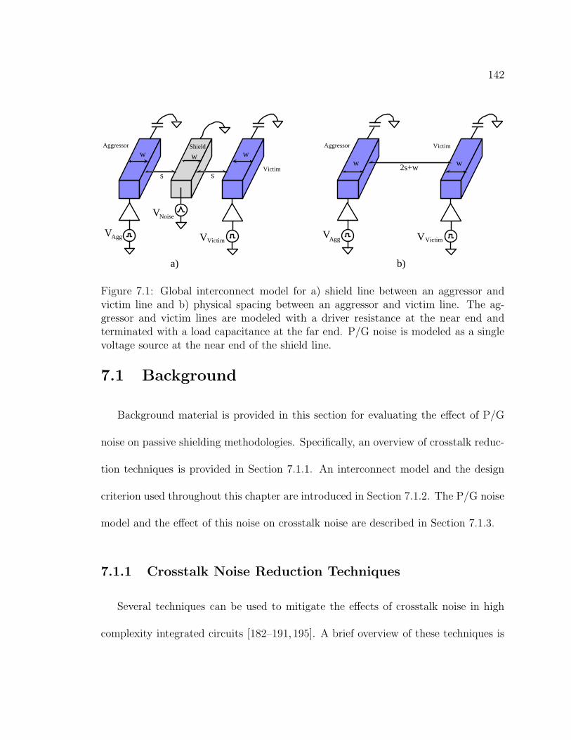
142
V
ss
ww wAggressor
Victim
Shield
a)
2s+ww w
b)
Noise
VictimV AggVVictimV
Aggressor Victim
Agg
V
Figure 7.1: Global interconnect model for a) shield line between an aggressor andvictim line and b) physical spacing between an aggressor and victim line. The ag-gressor and victim lines are modeled with a driver resistance at the near end andterminated with a load capacitance at the far end. P/G noise is modeled as a singlevoltage source at the near end of the shield line.
7.1 Background
Background material is provided in this section for evaluating the effect of P/G
noise on passive shielding methodologies. Specifically, an overview of crosstalk reduc-
tion techniques is provided in Section 7.1.1. An interconnect model and the design
criterion used throughout this chapter are introduced in Section 7.1.2. The P/G noise
model and the effect of this noise on crosstalk noise are described in Section 7.1.3.
7.1.1 Crosstalk Noise Reduction Techniques
Several techniques can be used to mitigate the effects of crosstalk noise in high
complexity integrated circuits [182–191, 195]. A brief overview of these techniques is

143
provided in this section.
Increasing the physical distance between the aggressor and victim lines can re-
duce the coupling capacitance and mutual inductance between adjacent lines. The
reduction in crosstalk capacitance is approximately inversely proportional with the
increase in spacing. The mutual inductance, however, is not significantly reduced
with increasing distance since the mutual inductance is a long range phenomenon.
To reduce the mutual inductance, additional return paths should be provided for the
current to flow.
Inserting shield lines between the aggressor and victim lines reduces the capaci-
tive and inductive coupling between adjacent blocks [183–188]. Shield insertion sig-
nificantly reduces capacitive coupling between the aggressor and victim lines because
capacitive coupling is a short range phenomenon and is significantly reduced in non-
adjacent lines. Shield insertion moderately reduces the mutual inductance due to
the current return path formed by the inserted shield line for both the aggressor and
victim lines [188]. The difficulty in forcing the current return path complicates the
inductive shielding process.
Active shielding is another shielding technique in which the shield line switches
depending upon the switching pattern of the adjacent bus lines [189–191]. Capacitive
(inductive) coupling is reduced with active shielding when the shield line is switched
in the same (opposite) direction as the signal line [190]. The switching activity of

144
the shield lines should therefore be tuned to the switching pattern which is different
for RC dominated and LC dominated interconnect lines. The primary drawback
of active shielding is increased power consumption and additional area of the logic
circuitry controlling the active shield lines. Furthermore, process and environmental
variations may unexpectedly affect the signal arrival times, degrading the efficiency
of active shielding.
Sizing the buffer driving the aggressor and victim lines is another technique to
reduce crosstalk noise [187]. The effective conductance of the driver increases with
larger drivers. For the victim line, a larger driver can be used to maintain the victim
line at a constant voltage by increasing the driver conductance. For the aggressor
line, using a smaller driver decreases the crosstalk noise since the signal transition is
slower due to the increased RC time constant, decreasing the induced noise on the
victim line [187]. Proper sizing of the driver on the aggressor and victim lines can
therefore produce lower crosstalk noise. This technique is however subject to delay
constraints since a smaller driver increases the gate delay. Wire sizing can also be used
to modify the line resistance, coupling capacitance, line-to-substrate capacitance, and
self-inductance [198].
Repeater insertion is used to reduce the length of the long interconnect to de-
crease the line resistance and the coupling capacitance and mutual inductance be-
tween lines [199]. Since the length of the switching portions of the adjacent lines
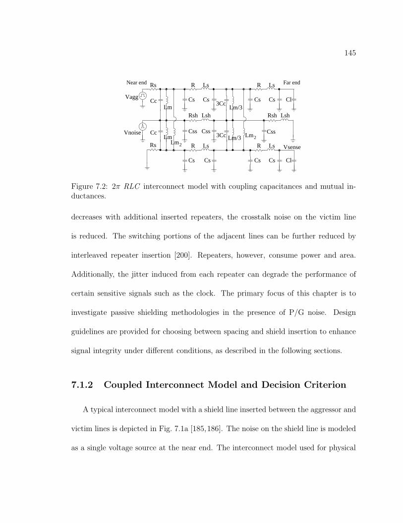
145
Rs
Lm
LmCss
RsNear end
Vagg
Vnoise
Far end
3CcLm/3
Lm/33Cc Lm2Lm2
Cs
CsCs Cs Cs Cl
ClCsCs
Css Css
CsCc
Cc
LsRLsR
LsRLsR
Rsh LshRshLsh
Vsense
Figure 7.2: 2π RLC interconnect model with coupling capacitances and mutual in-ductances.
decreases with additional inserted repeaters, the crosstalk noise on the victim line
is reduced. The switching portions of the adjacent lines can be further reduced by
interleaved repeater insertion [200]. Repeaters, however, consume power and area.
Additionally, the jitter induced from each repeater can degrade the performance of
certain sensitive signals such as the clock. The primary focus of this chapter is to
investigate passive shielding methodologies in the presence of P/G noise. Design
guidelines are provided for choosing between spacing and shield insertion to enhance
signal integrity under different conditions, as described in the following sections.
7.1.2 Coupled Interconnect Model and Decision Criterion
A typical interconnect model with a shield line inserted between the aggressor and
victim lines is depicted in Fig. 7.1a [185,186]. The noise on the shield line is modeled
as a single voltage source at the near end. The interconnect model used for physical
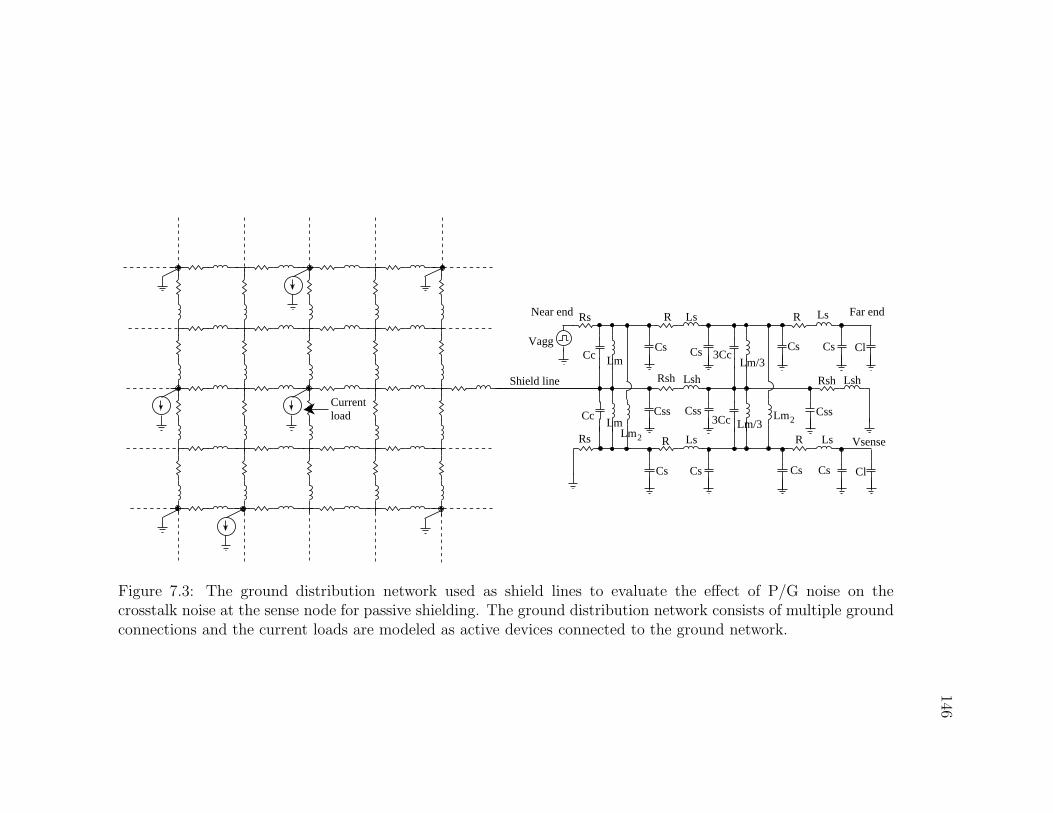
146
CsCsCsCs
Rs
Cc
CcLm
R
Lsh LshRsh
Css Css Css
Rs
Cs Cs Cl
Cl
Cs
Near end
Vagg
Far end
3CcLm/3
Lm/3
R Ls
VsenseLsR
3Cc
Ls
Cs
LsR
Rsh
Lm
Lm
Lm
Currentload
Shield line
2
2
Figure 7.3: The ground distribution network used as shield lines to evaluate the effect of P/G noise on thecrosstalk noise at the sense node for passive shielding. The ground distribution network consists of multiple groundconnections and the current loads are modeled as active devices connected to the ground network.

147
spacing is depicted in Fig. 7.1b.
The objective is to compare the effect of inserting a shield line and physical spacing
on the coupling noise at the far end of a victim line (sense node). The ratio K
of the total coupling noise at the sense node when only a shield line is present,
Vsense with shielding, to the total coupling noise when only physical spacing is used,
Vsense with spacing, is the decision criterion used to determine the boundary conditions,
K =Vsense with shielding
Vsense with spacing. (7.1)
If K < 1, inserting a shield line between the aggressor and victim lines is prefer-
able because the crosstalk noise at the sense node is smaller with a shield than with
additional spacing. Alternatively, if K > 1, increasing the spacing is a more effective
technique. K = 1 is therefore treated as a design threshold. Spacing is more efficient
above the threshold while shield insertion is more efficient below the threshold. Note
that the area is maintained the same for both shield insertion and physical spacing
to provide a fair comparison. The distance between the aggressor and victim lines is
the same for both shield insertion and physical spacing, as depicted in Fig. 7.1. For
instance, when the width of the shield line increases by ∆w, the distance between
the aggressor and victim lines increases by ∆w/2 to maintain unaltered the distance
between the shield line and the aggressor and victim lines. When comparing the
148
effectiveness of shield insertion with physical spacing for a specific example, the dis-
tance between the aggressor and victim lines is increased by ∆w to satisfy the same
area constraints for both the shielding and spacing methods. Alternatively, when
the distance between the aggressor and victim lines is increased using the spacing
method, the distance between the shield line and the aggressor and victim lines is
also increased with the shield insertion method to maintain the same area constraints.
To accurately investigate the effects of inductive and capacitive coupling, the 2π
RLC interconnect model [185] shown in Fig. 7.2 is used. The aggressor and victim line
parameters, Rs, R, Cs, Cc, Cl, and Ls, represent the interconnect driver resistance,
line resistance, line-to-substrate capacitance, coupling capacitance, load capacitance,
and self-inductance, respectively. Additional parameters, Rsh, Lsh, Css, Lm, and
Lm2, represent the shield resistance, shield self-inductance, shield line-to-substrate
capacitance, mutual inductance between the shield line and the aggressor and victim
lines, and mutual inductance between the aggressor and victim lines, respectively.
These circuit parameters have been extracted using the IBM Electromagnetic Field
Solver Suite Tools (EIP) [201] for the 32 nm, 45 nm, and 65 nm technology nodes [121,
202–204] for the parameters tabulated in Table 7.1. The operating frequency is 1 Ghz
with 100 ps rise and fall transition times. The supply voltage is 1 volt, 0.95 volts,
and 0.9 volts for the 65 nm, 45 nm, and 32 nm technology nodes, respectively.
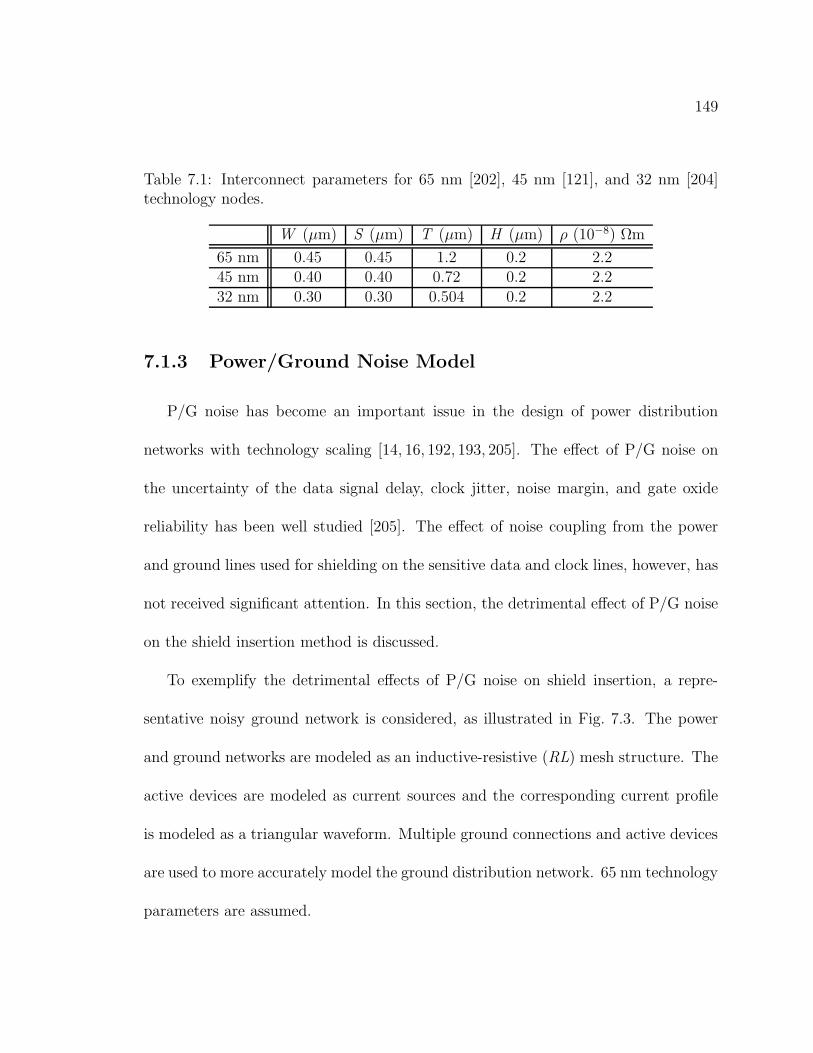
149
Table 7.1: Interconnect parameters for 65 nm [202], 45 nm [121], and 32 nm [204]technology nodes.
W (µm) S (µm) T (µm) H (µm) ρ (10−8) Ωm
65 nm 0.45 0.45 1.2 0.2 2.245 nm 0.40 0.40 0.72 0.2 2.232 nm 0.30 0.30 0.504 0.2 2.2
7.1.3 Power/Ground Noise Model
P/G noise has become an important issue in the design of power distribution
networks with technology scaling [14, 16, 192, 193, 205]. The effect of P/G noise on
the uncertainty of the data signal delay, clock jitter, noise margin, and gate oxide
reliability has been well studied [205]. The effect of noise coupling from the power
and ground lines used for shielding on the sensitive data and clock lines, however, has
not received significant attention. In this section, the detrimental effect of P/G noise
on the shield insertion method is discussed.
To exemplify the detrimental effects of P/G noise on shield insertion, a repre-
sentative noisy ground network is considered, as illustrated in Fig. 7.3. The power
and ground networks are modeled as an inductive-resistive (RL) mesh structure. The
active devices are modeled as current sources and the corresponding current profile
is modeled as a triangular waveform. Multiple ground connections and active devices
are used to more accurately model the ground distribution network. 65 nm technology
parameters are assumed.
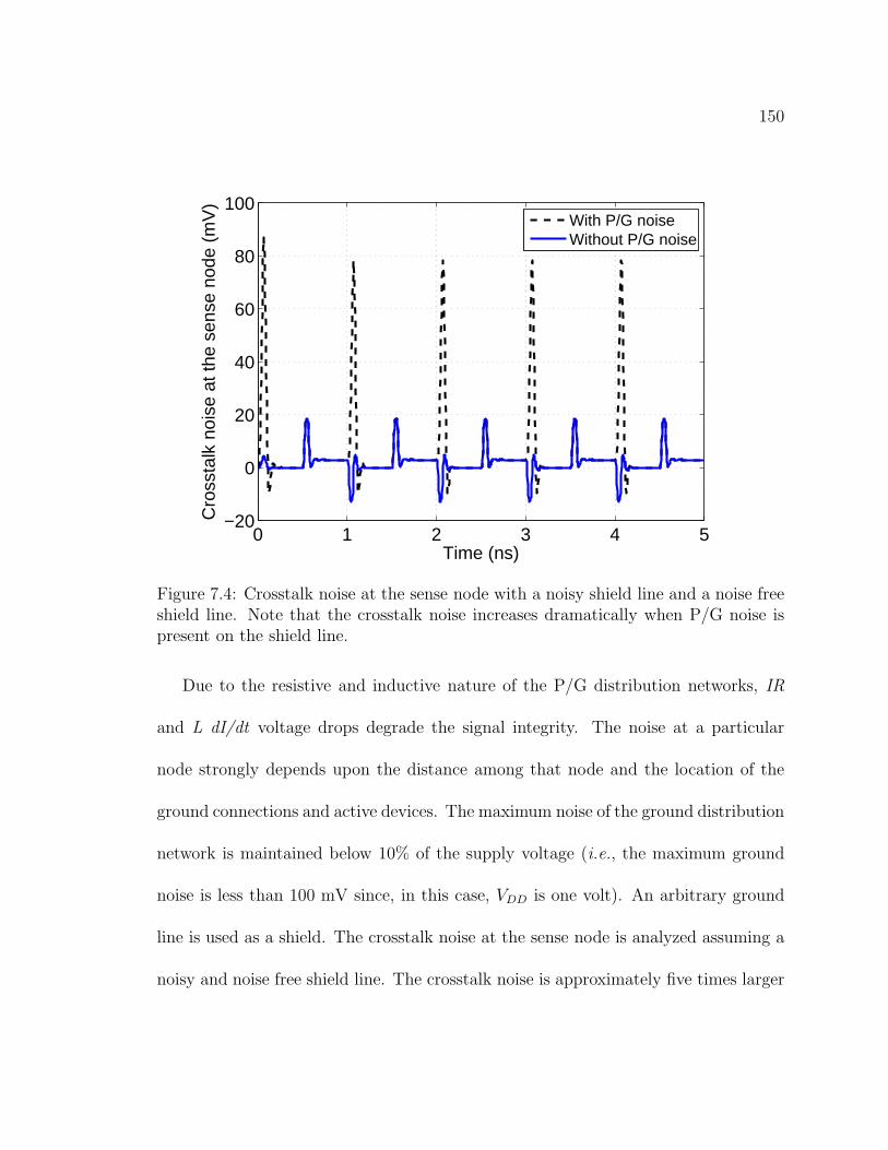
150
0 1 2 3 4 5−20
0
20
40
60
80
100
Time (ns)
Cro
ssta
lk n
oise
at t
he s
ense
nod
e (m
V)
With P/G noiseWithout P/G noise
Figure 7.4: Crosstalk noise at the sense node with a noisy shield line and a noise freeshield line. Note that the crosstalk noise increases dramatically when P/G noise ispresent on the shield line.
Due to the resistive and inductive nature of the P/G distribution networks, IR
and L dI/dt voltage drops degrade the signal integrity. The noise at a particular
node strongly depends upon the distance among that node and the location of the
ground connections and active devices. The maximum noise of the ground distribution
network is maintained below 10% of the supply voltage (i.e., the maximum ground
noise is less than 100 mV since, in this case, VDD is one volt). An arbitrary ground
line is used as a shield. The crosstalk noise at the sense node is analyzed assuming a
noisy and noise free shield line. The crosstalk noise is approximately five times larger
151
when the shield line is noisy as compared to a noise free shield line, as illustrated in
Fig. 7.4. Note that the detrimental effect of the P/G noise is significant for a system
even when the ground noise is less than 10% of the supply voltage. With continuous
scaling of the supply voltage with each technology generation, the relative magnitude
of the P/G noise to the supply voltage makes the victim lines increasingly sensitive
to noise on the shield line.
7.2 Effects of Technology and Design Parameters
on the Crosstalk Noise Voltage
Interconnect capacitance, inductance, and resistance increase with the length of
the interconnect. The substrate and coupling capacitances increase and the self-
inductance slightly decreases for wider interconnect. The coupling capacitance in-
creases and the self-inductance slightly decreases for thicker interconnects. When
the distance between adjacent interconnects increases, the coupling capacitance and
mutual inductance decrease and the substrate capacitance increases. These trends
are listed in Table 7.2.
The effects of technology scaling on the crosstalk noise voltage and the shield
insertion process are discussed in Section 7.2.1. The effects of the interconnect line
length and shield line width on the crosstalk noise are discussed in Sections 7.2.2
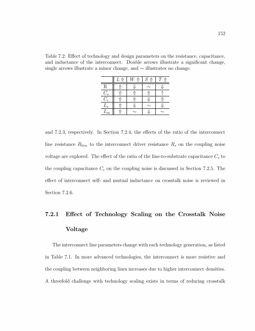
152
Table 7.2: Effect of technology and design parameters on the resistance, capacitance,and inductance of the interconnect. Double arrows illustrate a significant change,single arrows illustrate a minor change, and ∼ illustrates no change.
L ⇑ W ⇑ S ⇑ T ⇑R ⇑ ⇓ ∼ ⇓Cs ⇑ ⇑ ⇑ ↑Cc ⇑ ⇑ ⇓ ⇑Ls ⇑ ⇓ ∼ ⇓Lm ⇑ ∼ ⇓ ∼
and 7.2.3, respectively. In Section 7.2.4, the effects of the ratio of the interconnect
line resistance Rline to the interconnect driver resistance Rs on the coupling noise
voltage are explored. The effect of the ratio of the line-to-substrate capacitance Cs to
the coupling capacitance Cc on the coupling noise is discussed in Section 7.2.5. The
effect of interconnect self- and mutual inductance on crosstalk noise is reviewed in
Section 7.2.6.
7.2.1 Effect of Technology Scaling on the Crosstalk Noise
Voltage
The interconnect line parameters change with each technology generation, as listed
in Table 7.1. In more advanced technologies, the interconnect is more resistive and
the coupling between neighboring lines increases due to higher interconnect densities.
A threefold challenge with technology scaling exists in terms of reducing crosstalk
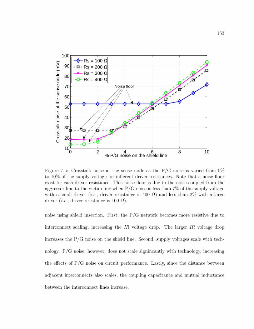
153
0 2 4 6 8 1010
20
30
40
50
60
70
80
90
100
% P/G noise on the shield line
Cro
ssta
lk n
oise
at t
he s
ense
nod
e (m
V)
Rs = 100 ΩRs = 200 ΩRs = 300 ΩRs = 400 Ω
Noise floor
Figure 7.5: Crosstalk noise at the sense node as the P/G noise is varied from 0%to 10% of the supply voltage for different driver resistances. Note that a noise floorexist for each driver resistance. This noise floor is due to the noise coupled from theaggressor line to the victim line when P/G noise is less than 7% of the supply voltagewith a small driver (i.e., driver resistance is 400 Ω) and less than 2% with a largedriver (i.e., driver resistance is 100 Ω).
noise using shield insertion. First, the P/G network becomes more resistive due to
interconnect scaling, increasing the IR voltage drop. The larger IR voltage drop
increases the P/G noise on the shield line. Second, supply voltages scale with tech-
nology. P/G noise, however, does not scale significantly with technology, increasing
the effects of P/G noise on circuit performance. Lastly, since the distance between
adjacent interconnects also scales, the coupling capacitance and mutual inductance
between the interconnect lines increase.
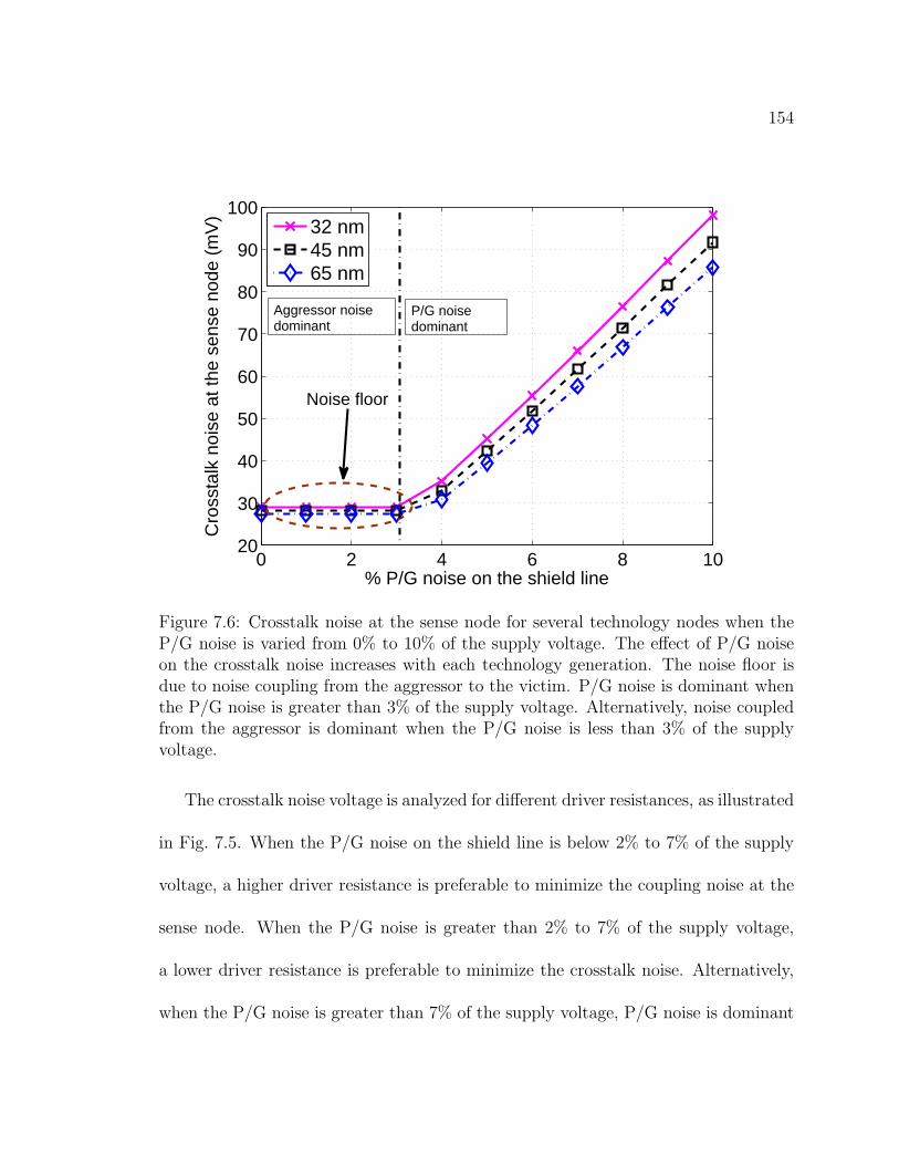
154
0 2 4 6 8 1020
30
40
50
60
70
80
90
100
% P/G noise on the shield line
Cro
ssta
lk n
oise
at t
he s
ense
nod
e (m
V)
32 nm45 nm65 nm
Noise floor
Aggressor noisedominant
P/G noisedominant
Figure 7.6: Crosstalk noise at the sense node for several technology nodes when theP/G noise is varied from 0% to 10% of the supply voltage. The effect of P/G noiseon the crosstalk noise increases with each technology generation. The noise floor isdue to noise coupling from the aggressor to the victim. P/G noise is dominant whenthe P/G noise is greater than 3% of the supply voltage. Alternatively, noise coupledfrom the aggressor is dominant when the P/G noise is less than 3% of the supplyvoltage.
The crosstalk noise voltage is analyzed for different driver resistances, as illustrated
in Fig. 7.5. When the P/G noise on the shield line is below 2% to 7% of the supply
voltage, a higher driver resistance is preferable to minimize the coupling noise at the
sense node. When the P/G noise is greater than 2% to 7% of the supply voltage,
a lower driver resistance is preferable to minimize the crosstalk noise. Alternatively,
when the P/G noise is greater than 7% of the supply voltage, P/G noise is dominant
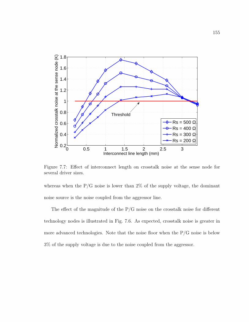
155
0 0.5 1 1.5 2 2.5 30.2
0.4
0.6
0.8
1
1.2
1.4
1.6
1.8
Interconnect line length (mm)
Nor
mal
ized
cro
ssta
lk n
oise
at t
he s
ense
nod
e (K
)
Rs = 500 ΩRs = 400 ΩRs = 300 ΩRs = 200 Ω
Threshold
Figure 7.7: Effect of interconnect length on crosstalk noise at the sense node forseveral driver sizes.
whereas when the P/G noise is lower than 2% of the supply voltage, the dominant
noise source is the noise coupled from the aggressor line.
The effect of the magnitude of the P/G noise on the crosstalk noise for different
technology nodes is illustrated in Fig. 7.6. As expected, crosstalk noise is greater in
more advanced technologies. Note that the noise floor when the P/G noise is below
3% of the supply voltage is due to the noise coupled from the aggressor.

156
7.2.2 Effect of Line Length on Crosstalk Noise
The length of the global interconnect typically increases with technology scaling,
causing greater signal noise [79,195,199]. The global interconnect can be longer than
4 mm [79,195,199]. Repeater insertion minimizes the crosstalk noise and delay of the
long interconnect. Inserting repeaters along the wide and thick global interconnects,
however, can cause wire and via congestion as well as dissipate high power [199]. The
wire resistance, substrate capacitance, self-inductance of a wire, coupling capacitance,
and mutual inductance between neighboring wires increase with longer line length.
For the interconnect model shown in Fig. 7.2, the coupling noise voltage at the
sense node is compared to shield insertion and physical spacing for different intercon-
nect lengths and driver resistances. These results are illustrated in Fig. 7.7, where
K=1 is the threshold (the same noise at the sense node occurs for both physical
spacing and shield insertion).
At the 65 nm technology node, the peak value of K occurs at an interconnect
length of 1.4 mm. K monotonically increases for interconnect lines shorter than 1.4
mm and monotonically decreases for interconnect lines longer than 1.4 mm. The
crosstalk noise occurring at the sense node with physical spacing and shield insertion
is shown in Figs. 7.8a and 7.8b, respectively. The crosstalk noise at the sense node
with physical spacing monotonically decreases with longer interconnect length. The
crosstalk noise with shield insertion, however, exhibits a non-monotonic behavior
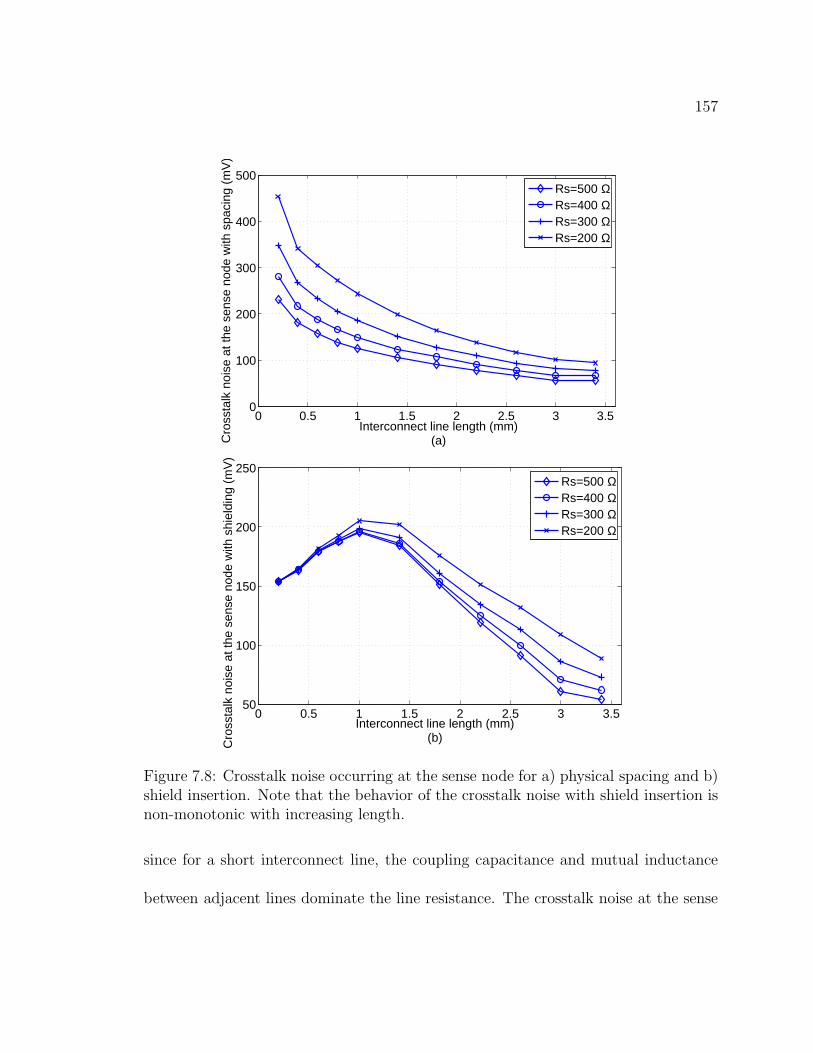
157
0 0.5 1 1.5 2 2.5 3 3.50
100
200
300
400
500
Interconnect line length (mm)(a)C
ross
talk
noi
se a
t the
sen
se n
ode
with
spa
cing
(m
V)
Rs=500 ΩRs=400 ΩRs=300 ΩRs=200 Ω
0 0.5 1 1.5 2 2.5 3 3.550
100
150
200
250
Interconnect line length (mm)(b)C
ross
talk
noi
se a
t the
sen
se n
ode
with
shi
eldi
ng (
mV
)
Rs=500 ΩRs=400 ΩRs=300 ΩRs=200 Ω
Figure 7.8: Crosstalk noise occurring at the sense node for a) physical spacing and b)shield insertion. Note that the behavior of the crosstalk noise with shield insertion isnon-monotonic with increasing length.
since for a short interconnect line, the coupling capacitance and mutual inductance
between adjacent lines dominate the line resistance. The crosstalk noise at the sense

158
Table 7.3: Critical line length and driver resistance for several advanced technologynodes. Below the critical line length, shield insertion is preferable. Physical spacingis preferable for those interconnect lines longer than the critical line length.
65 nm 45 nm 32 nmDriver resistance (ohm) 100 200 300 400 100 200 300 400 100 200 300 400
Critical line length (mm) 1.4 1.3 1 0.8 1.3 1.1 0.9 0.8 1.3 0.8 0.2 0.1
node, as shown in Fig. 7.8b, begins to decrease once the distance between the near and
far end of the interconnect line is longer than the length where the effect of the line
resistance dominates the effect of the coupling capacitance and mutual inductance
(i.e., 1.4 mm for a 65 nm technology). Also note in Fig. 7.8 that inserting a shield
line mitigates the effect of the driver resistance on the crosstalk noise, as discussed in
Section 7.2.4. As a result, shield insertion is preferable for shorter lines and spacing
is preferable for longer lines.
The effect of interconnect length is considered for different technology nodes. The
critical interconnect length is determined for different driver resistances, as tabulated
in Table 7.3. With each technology generation, the width and thickness of the inter-
connect scale with the minimum feature size. Since the line resistance increases with
each technology generation, larger drivers (e.g., drivers with lower resistance) should
be used to drive long victim lines. As listed in Table 7.3, shield insertion is more
effective when both the aggressor and victim lines are driven by a large driver.

159
7.2.3 Effect of Shield Line Width on Crosstalk Noise
The effect of the cross-sectional area of the shield line on the coupling noise is
discussed in this subsection. As the lines become more narrow and thin, the line
resistance increases and the self-inductance decreases, making the lines more resistive.
The coupling capacitance and mutual inductance between the shield line and the
adjacent interconnect do not change significantly. To determine the effect of the
cross-sectional area of the shield line on the crosstalk noise, the width of the shield
line is evaluated for several driver resistances and interconnect lengths. A comparison
of shield insertion and physical spacing is illustrated in Fig. 7.9 for a 1 mm long
interconnect. Note that the distance between the aggressor and victim lines remains
the same for both the physical spacing and shield insertion methods.
As the shield line width increases, shield insertion becomes less effective. Although
increasing the width lowers the coupling from the aggressor to the sense node, P/G
noise coupling to the sense node increases due to the lower resistance of the shield
line and the higher mutual inductance. The P/G noise on the shield line propagates
from the near end to the far end with less attenuation.
7.2.4 Effect of Rline/Rs on Crosstalk Noise
The driver resistance has a substantial effect on the behavior of global intercon-
nects [206–208]. The driver resistance is less affected with technology scaling [209]
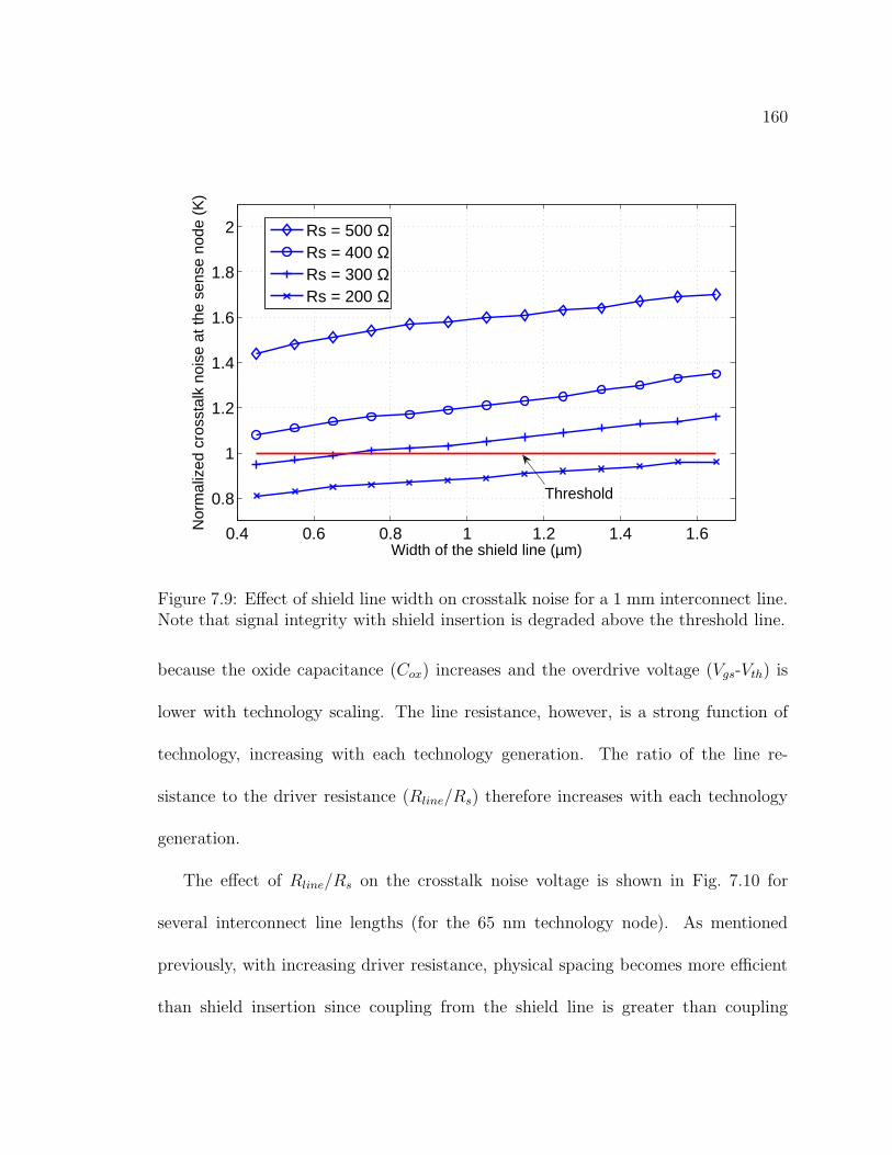
160
0.4 0.6 0.8 1 1.2 1.4 1.6
0.8
1
1.2
1.4
1.6
1.8
2
Width of the shield line (µm)
Nor
mal
ized
cro
ssta
lk n
oise
at t
he s
ense
nod
e (K
)
Rs = 500 ΩRs = 400 ΩRs = 300 ΩRs = 200 Ω
Threshold
Figure 7.9: Effect of shield line width on crosstalk noise for a 1 mm interconnect line.Note that signal integrity with shield insertion is degraded above the threshold line.
because the oxide capacitance (Cox) increases and the overdrive voltage (Vgs-Vth) is
lower with technology scaling. The line resistance, however, is a strong function of
technology, increasing with each technology generation. The ratio of the line re-
sistance to the driver resistance (Rline/Rs) therefore increases with each technology
generation.
The effect of Rline/Rs on the crosstalk noise voltage is shown in Fig. 7.10 for
several interconnect line lengths (for the 65 nm technology node). As mentioned
previously, with increasing driver resistance, physical spacing becomes more efficient
than shield insertion since coupling from the shield line is greater than coupling
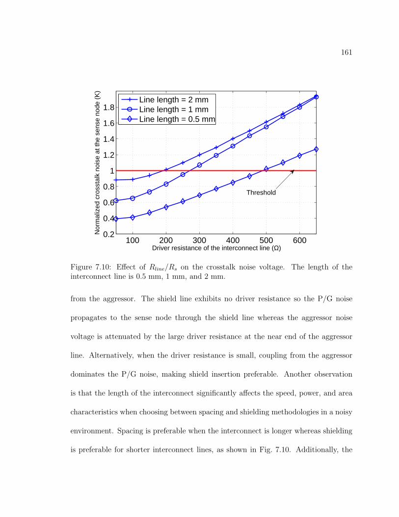
161
100 200 300 400 500 6000.2
0.4
0.6
0.8
1
1.2
1.4
1.6
1.8
Driver resistance of the interconnect line (Ω)
Nor
mal
ized
cro
ssta
lk n
oise
at t
he s
ense
nod
e (K
)
Line length = 2 mmLine length = 1 mmLine length = 0.5 mm
Threshold
Figure 7.10: Effect of Rline/Rs on the crosstalk noise voltage. The length of theinterconnect line is 0.5 mm, 1 mm, and 2 mm.
from the aggressor. The shield line exhibits no driver resistance so the P/G noise
propagates to the sense node through the shield line whereas the aggressor noise
voltage is attenuated by the large driver resistance at the near end of the aggressor
line. Alternatively, when the driver resistance is small, coupling from the aggressor
dominates the P/G noise, making shield insertion preferable. Another observation
is that the length of the interconnect significantly affects the speed, power, and area
characteristics when choosing between spacing and shielding methodologies in a noisy
environment. Spacing is preferable when the interconnect is longer whereas shielding
is preferable for shorter interconnect lines, as shown in Fig. 7.10. Additionally, the

162
Rline/Rs ratio increases in more advanced technologies. The crosstalk noise voltage is
therefore more sensitive to P/G noise on the shield line. Either the driver resistance
or the line width should be reduced in more advanced technologies.
7.2.5 Effect of the Ratio of Substrate Capacitance to Cou-
pling Capacitance on Crosstalk Noise
The coupling capacitance between adjacent interconnect strongly depends upon
the switching activity of the wires [210]. When the signals driving the adjacent lines
switch in the same direction, the coupling capacitance is the same as the coupling
capacitance between two adjacent quiet lines. When the signals driving the adjacent
lines switch in the opposite direction, the coupling capacitance between the adjacent
lines is two times the capacitance when only one of the adjacent lines is switching [210,
211].
The effect of the ratio of the line-to-substrate capacitance to the coupling capaci-
tance has been evaluated for active and passive shielding structures [191], but without
considering P/G noise on the shield lines. The effect of this ratio on the crosstalk noise
at the sense node for different driver resistances is depicted in Figs. 7.11 and 7.12 for
interconnect line lengths of 0.5 mm and 1 mm, respectively. When the coupling ca-
pacitance is greater than the line-to-substrate capacitance, shield insertion is more ef-
fective than additional spacing. As the line-to-substrate capacitance becomes greater
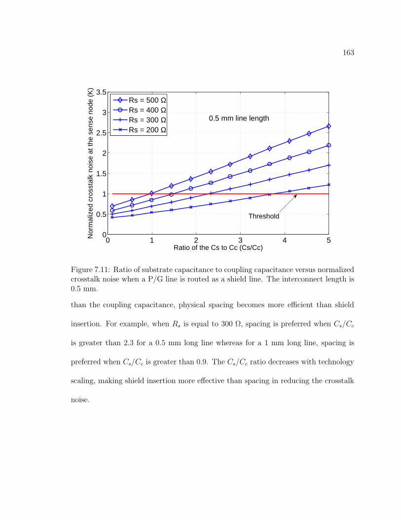
163
0 1 2 3 4 50
0.5
1
1.5
2
2.5
3
3.5
Ratio of the Cs to Cc (Cs/Cc)
Nor
mal
ized
cro
ssta
lk n
oise
at t
he s
ense
nod
e (K
)
Rs = 500 ΩRs = 400 ΩRs = 300 ΩRs = 200 Ω
0.5 mm line length
Threshold
Figure 7.11: Ratio of substrate capacitance to coupling capacitance versus normalizedcrosstalk noise when a P/G line is routed as a shield line. The interconnect length is0.5 mm.
than the coupling capacitance, physical spacing becomes more efficient than shield
insertion. For example, when Rs is equal to 300 Ω, spacing is preferred when Cs/Cc
is greater than 2.3 for a 0.5 mm long line whereas for a 1 mm long line, spacing is
preferred when Cs/Cc is greater than 0.9. The Cs/Cc ratio decreases with technology
scaling, making shield insertion more effective than spacing in reducing the crosstalk
noise.
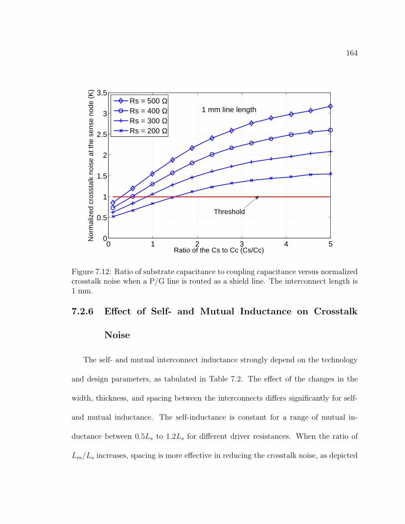
164
0 1 2 3 4 50
0.5
1
1.5
2
2.5
3
3.5
Ratio of the Cs to Cc (Cs/Cc)
Nor
mal
ized
cro
ssta
lk n
oise
at t
he s
ense
nod
e (K
)
Rs = 500 ΩRs = 400 ΩRs = 300 ΩRs = 200 Ω
Threshold
1 mm line length
Figure 7.12: Ratio of substrate capacitance to coupling capacitance versus normalizedcrosstalk noise when a P/G line is routed as a shield line. The interconnect length is1 mm.
7.2.6 Effect of Self- and Mutual Inductance on Crosstalk
Noise
The self- and mutual interconnect inductance strongly depend on the technology
and design parameters, as tabulated in Table 7.2. The effect of the changes in the
width, thickness, and spacing between the interconnects differs significantly for self-
and mutual inductance. The self-inductance is constant for a range of mutual in-
ductance between 0.5Ls to 1.2Ls for different driver resistances. When the ratio of
Lm/Ls increases, spacing is more effective in reducing the crosstalk noise, as depicted
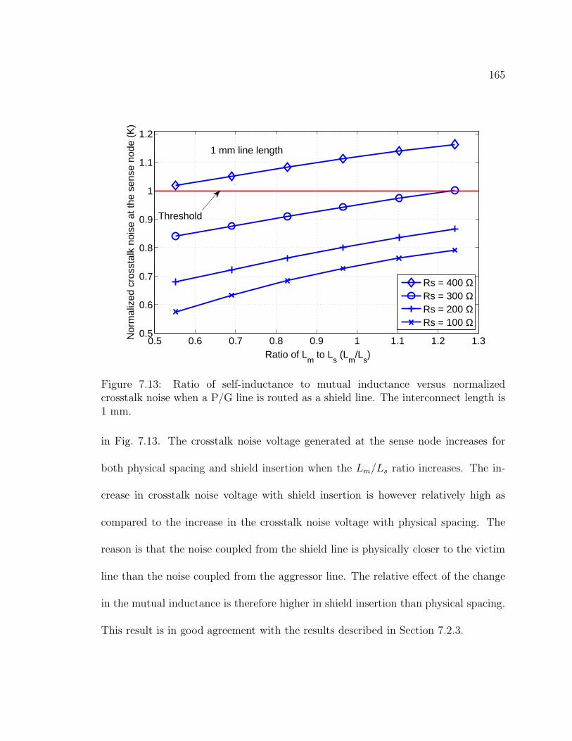
165
0.5 0.6 0.7 0.8 0.9 1 1.1 1.2 1.30.5
0.6
0.7
0.8
0.9
1
1.1
1.2
Ratio of Lm
to Ls (L
m/L
s)
Nor
mal
ized
cro
ssta
lk n
oise
at t
he s
ense
nod
e (K
)
Rs = 400 ΩRs = 300 ΩRs = 200 ΩRs = 100 Ω
Threshold
1 mm line length
Figure 7.13: Ratio of self-inductance to mutual inductance versus normalizedcrosstalk noise when a P/G line is routed as a shield line. The interconnect length is1 mm.
in Fig. 7.13. The crosstalk noise voltage generated at the sense node increases for
both physical spacing and shield insertion when the Lm/Ls ratio increases. The in-
crease in crosstalk noise voltage with shield insertion is however relatively high as
compared to the increase in the crosstalk noise voltage with physical spacing. The
reason is that the noise coupled from the shield line is physically closer to the victim
line than the noise coupled from the aggressor line. The relative effect of the change
in the mutual inductance is therefore higher in shield insertion than physical spacing.
This result is in good agreement with the results described in Section 7.2.3.

166
7.2.7 Effect of Distance between Aggressor and Victim Lines
on Crosstalk Noise
The crosstalk noise at the sense node is inversely proportional to the distance
between the aggressor and victim lines since the coupling capacitance and mutual
inductance decreases with increasing separation between lines. In this section, the
effectiveness of shield insertion in a noisy environment is discussed. Lm decreases with
greater separation between adjacent wires, lowering the Lm/Ls ratio. Alternatively,
the Cs/Cc ratio increases with higher separation. Shield insertion is more efficient
with a smaller Lm/Ls ratio. Conversely, additional spacing is preferable with a higher
Cs/Cc ratio. The ratio Vsense with shielding/Vsense with spacing, denoted as K, therefore
does not change significantly with increasing separation between the aggressor and
victim lines. The distance between the aggressor and victim lines is varied from 0.8
µm to 2 µm, where the ratio of the crosstalk noise generated at the sense node with
both shield insertion and spacing is shown in Fig. 7.14. Note that when comparing
the effectiveness of shield insertion to physical spacing, the separation between the
aggressor and victim lines is the same for both techniques.
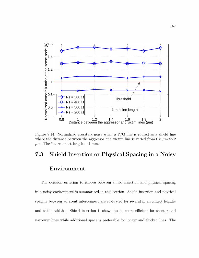
167
0.8 1 1.2 1.4 1.6 1.8 2
0.6
0.8
1
1.2
1.4
1.6
Distance between the aggressor and victim lines (µm)
Nor
mal
ized
cro
ssta
lk n
oise
at t
he s
ense
nod
e (K
)
Rs = 500 ΩRs = 400 ΩRs = 300 ΩRs = 200 Ω
Threshold
1 mm line length
Figure 7.14: Normalized crosstalk noise when a P/G line is routed as a shield linewhere the distance between the aggressor and victim line is varied from 0.8 µm to 2µm. The interconnect length is 1 mm.
7.3 Shield Insertion or Physical Spacing in a Noisy
Environment
The decision criterion to choose between shield insertion and physical spacing
in a noisy environment is summarized in this section. Shield insertion and physical
spacing between adjacent interconnect are evaluated for several interconnect lengths
and shield widths. Shield insertion is shown to be more efficient for shorter and
narrower lines while additional space is preferable for longer and thicker lines. The
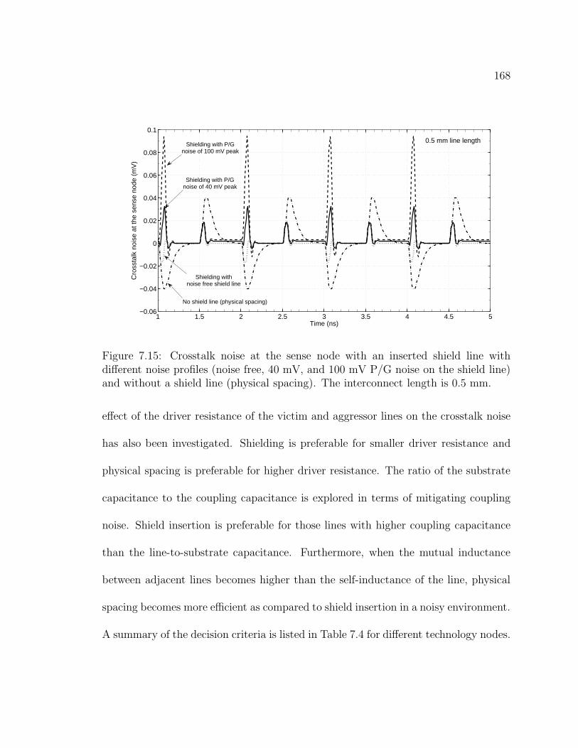
168
1 1.5 2 2.5 3 3.5 4 4.5 5−0.06
−0.04
−0.02
0
0.02
0.04
0.06
0.08
0.1
Time (ns)
Cro
ssta
lk n
oise
at t
he s
ense
nod
e (m
V)
No shield line (physical spacing)
Shielding withnoise free shield line
Shielding with P/Gnoise of 40 mV peak
Shielding with P/Gnoise of 100 mV peak
0.5 mm line length
Figure 7.15: Crosstalk noise at the sense node with an inserted shield line withdifferent noise profiles (noise free, 40 mV, and 100 mV P/G noise on the shield line)and without a shield line (physical spacing). The interconnect length is 0.5 mm.
effect of the driver resistance of the victim and aggressor lines on the crosstalk noise
has also been investigated. Shielding is preferable for smaller driver resistance and
physical spacing is preferable for higher driver resistance. The ratio of the substrate
capacitance to the coupling capacitance is explored in terms of mitigating coupling
noise. Shield insertion is preferable for those lines with higher coupling capacitance
than the line-to-substrate capacitance. Furthermore, when the mutual inductance
between adjacent lines becomes higher than the self-inductance of the line, physical
spacing becomes more efficient as compared to shield insertion in a noisy environment.
A summary of the decision criteria is listed in Table 7.4 for different technology nodes.
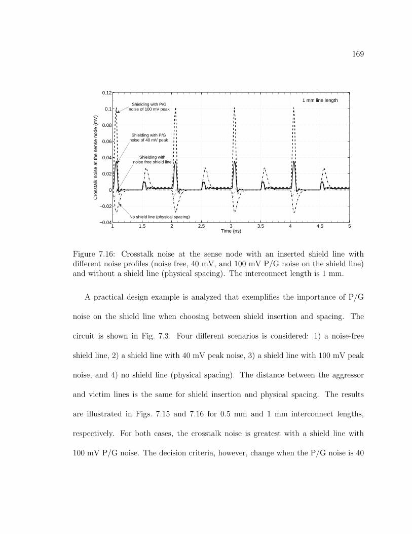
169
1 1.5 2 2.5 3 3.5 4 4.5 5−0.04
−0.02
0
0.02
0.04
0.06
0.08
0.1
0.12
Time (ns)
Cro
ssta
lk n
oise
at t
he s
ense
nod
e (m
V)
Shielding withnoise free shield line
Shielding with P/Gnoise of 100 mV peak
Shielding with P/Gnoise of 40 mV peak
No shield line (physical spacing)
1 mm line length
Figure 7.16: Crosstalk noise at the sense node with an inserted shield line withdifferent noise profiles (noise free, 40 mV, and 100 mV P/G noise on the shield line)and without a shield line (physical spacing). The interconnect length is 1 mm.
A practical design example is analyzed that exemplifies the importance of P/G
noise on the shield line when choosing between shield insertion and spacing. The
circuit is shown in Fig. 7.3. Four different scenarios is considered: 1) a noise-free
shield line, 2) a shield line with 40 mV peak noise, 3) a shield line with 100 mV peak
noise, and 4) no shield line (physical spacing). The distance between the aggressor
and victim lines is the same for shield insertion and physical spacing. The results
are illustrated in Figs. 7.15 and 7.16 for 0.5 mm and 1 mm interconnect lengths,
respectively. For both cases, the crosstalk noise is greatest with a shield line with
100 mV P/G noise. The decision criteria, however, change when the P/G noise is 40

170
Table 7.4: Decision criterion for the critical interconnect length (width), Rs = 300 Ω.Shield insertion is preferable when the interconnect length (width) is smaller than thecritical length (width). Spacing is preferable when the interconnect length (width) isgreater than the critical length (width).
Technology node Shielding Critical dimension Spacing
Lengtha
65 nm X < 1 mm <X
45 nm X < 0.9 mm <X
32 nm X < 0.2 mm <X
Widthb
65 nm X < 0.7 µm <X
45 nm X < 0.9 µm <X
32 nm X < 1.2 µm <X
aWidth is maintained at 1 µmbLength is maintained at 1 mm
mV. For a 0.5 mm line length, the maximum noise with a shield line is greater than
the noise without a shield line. The maximum noise with a 1 mm line is however
greater without a shield line as compared to a shield line with 40 mV P/G noise.
Additionally, when no P/G noise is present on the shield line, shield insertion is the
preferred design method to mitigate crosstalk noise.
Two of the most important parameters to consider when choosing between shield
insertion and physical spacing is the interconnect line length and the size of the tran-
sistors driving the aggressor and victim lines. For short interconnect lines, shield in-
sertion is preferable while physical spacing is preferred for longer lines. This decision,
however, also strongly depends upon the output resistance of the driver transistors
and the width of the interconnect lines, as explained in Section 7.2. When Rs becomes
smaller (i.e., a stronger driver strength), shield insertion is more efficient in reducing
171
crosstalk noise.
7.4 Summary
Shielding methodologies in the presence of P/G noise are introduced in this chap-
ter. With technology scaling, P/G noise has become a significant design issue. The
P/G network has become more resistive, increasing the noise within the P/G dis-
tribution network. Additionally, with supply voltage scaling, the noise of the P/G
network is more significant. The P/G noise on the shield line reduces the efficiency
of shielding because this noise also couples to the victim lines. P/G noise is the
dominant source of crosstalk noise when the noise is greater than 7% of the supply
voltage. Coupling from the aggressor to the victim is the dominant noise source when
the P/G noise is less than 2% of the supply voltage. The effect of technology scaling
on shield insertion in a noisy environment is also described.
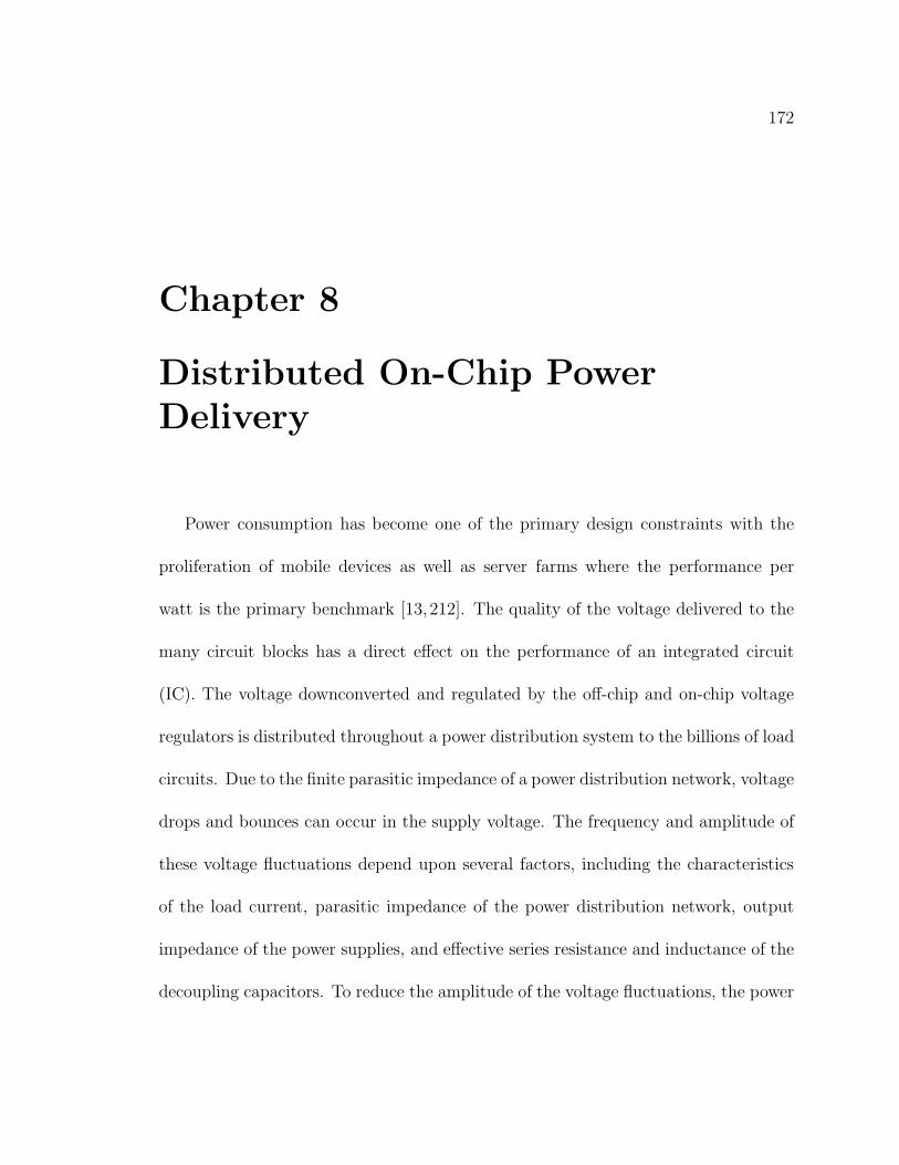
172
Chapter 8
Distributed On-Chip PowerDelivery
Power consumption has become one of the primary design constraints with the
proliferation of mobile devices as well as server farms where the performance per
watt is the primary benchmark [13, 212]. The quality of the voltage delivered to the
many circuit blocks has a direct effect on the performance of an integrated circuit
(IC). The voltage downconverted and regulated by the off-chip and on-chip voltage
regulators is distributed throughout a power distribution system to the billions of load
circuits. Due to the finite parasitic impedance of a power distribution network, voltage
drops and bounces can occur in the supply voltage. The frequency and amplitude of
these voltage fluctuations depend upon several factors, including the characteristics
of the load current, parasitic impedance of the power distribution network, output
impedance of the power supplies, and effective series resistance and inductance of the
decoupling capacitors. To reduce the amplitude of the voltage fluctuations, the power

173
supplies are supported by the locally distributed decoupling capacitors, which serve
as a nearby reservoir of charge, providing current to the load circuits [112].
The complexity of the high performance power delivery systems has increased
significantly with the integration of diverse technologies on a single die, forming a
heterogeneous system. The required voltage levels and noise constraints vary signifi-
cantly for different technologies. Novel voltage regulator topologies have recently been
proposed [24, 28, 30, 60, 213–215], enabling not only the integration of on-chip power
supplies but also multiple distributed on-chip point-of-load power supplies [215,216].
These on-chip point-of-load power supplies provide the necessary voltage close to the
load circuits, greatly reducing the parasitic impedance between the load circuits and
power supplies, and enhancing the efficiency of the overall power delivery system [217].
Next generation power delivery networks for high performance circuits will contain
tens to hundreds of on-chip power supplies supported by many thousands of on-chip
decoupling capacitors to satisfy the current demand of billions of load circuits within
different voltage islands, as illustrated in Fig. 8.1. The design of these complex
systems would be greatly enhanced if the available resources, such as the physical
area, number of metal layers, and power budget, were not severely limited. The
continuous demand over the past decade for greater functionality within a small form
factor has imposed tight resource constraints while achieving aggressive performance
and noise targets [218].
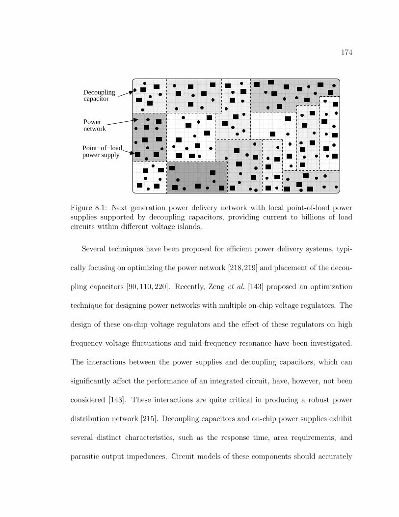
174
Point−of−loadpower supply
capacitorDecoupling
Powernetwork
Figure 8.1: Next generation power delivery network with local point-of-load powersupplies supported by decoupling capacitors, providing current to billions of loadcircuits within different voltage islands.
Several techniques have been proposed for efficient power delivery systems, typi-
cally focusing on optimizing the power network [218,219] and placement of the decou-
pling capacitors [90, 110, 220]. Recently, Zeng et al. [143] proposed an optimization
technique for designing power networks with multiple on-chip voltage regulators. The
design of these on-chip voltage regulators and the effect of these regulators on high
frequency voltage fluctuations and mid-frequency resonance have been investigated.
The interactions between the power supplies and decoupling capacitors, which can
significantly affect the performance of an integrated circuit, have, however, not been
considered [143]. These interactions are quite critical in producing a robust power
distribution network [215]. Decoupling capacitors and on-chip power supplies exhibit
several distinct characteristics, such as the response time, area requirements, and
parasitic output impedances. Circuit models of these components should accurately
175
capture these characteristics, while being sufficiently simple to not computationally
constrain the optimization process.
In this chapter, the optimum location of the on-chip power supplies and decoupling
capacitors for different constraints is determined using facility location optimization
algorithms [221–223]. The constraints of this power network co-design problem de-
pend upon the application and performance objectives. The optimization goal can
be to minimize the maximum voltage drop, total area, response time for particular
circuit blocks, or total power consumption. Multiple optimization goals can also be
applied for smaller or mid-size integrated circuits.
The rest of the chapter is organized as follows. A recently developed point-of-load
voltage regulator is briefly described in Section 8.1. The facility location problem is
introduced with some exemplary applications in Section 8.2. A proposed methodology
to determine the optimum location of the power supplies and decoupling capacitors is
examined in Section 8.3. The optimum location of the power supplies and decoupling
capacitors, exemplified on several benchmark circuits, is presented in Section 8.4. A
brief discussion of the proposed optimization technique and possible enhancements
are offered in Section 8.5. The chapter is concluded in Section 8.6.

176
8.1 Point-of-Load Voltage Regulators
Placing multiple point-of-load power supplies is challenging since the area occupied
by a single power supply should be small and the efficiency sufficiently high. Guo et
al. proposed an output capacitorless low-dropout regulator which occupies an on-chip
area of 0.019 mm2 [60]. The authors of this chapter recently proposed a hybrid point-
of-load voltage regulator, occupying an on-chip area of 0.015 mm2 [213,214,224,225].
A microphotograph of this hybrid point-of-load regulator is shown in Fig. 8.2. These
area efficient voltage regulators provide a means for distributing multiple local power
supplies across an integrated circuit, while maintaining high current efficiency and
small area. With point-of-load voltage delivery, on-chip signal and power integrity are
significantly enhanced while providing the capability for distributing multiple power
supplies. Design methodologies are therefore required to determine the location, size,
and number of these distributed on-chip power supplies and decoupling capacitors.
8.2 Facility Location Problem
Every complex system is an ensemble of small components, typically with simple
structures. The interactions and aggregation of these components form a highly
sophisticated system. The efficiency of this system strongly depends not only upon
the physical properties of the individual components but also on the spatial location

177
PWM
Passive RC
Op amp Op amp
output
stage
Output test pad
185 µm
80 µm
Figure 8.2: Microphotograph of the hybrid voltage regulator [213].
of these components since the placement of these components significantly affects
the multiple interactions within the system. In most systems, these components can
be grouped into two categories; (1) facilities, and (2) customers. Facility location
problems, to determine the location, size, and number of facilities that minimize the
cost of providing a high quality service to customers, have been well studied over the
last several decades [221].
Mathematical models have been widely used to determine the optimal number,
location, and size of the facilities as well as to allocate facility resources to those cus-
tomers that minimize or maximize an objective function [221–223]. The problem can
be categorized depending upon the interconnection network (discrete or continuous)
and the input (static or dynamic). The objective is typically to minimize the average
(or maximum) distance from the facilities to the customers, determine the minimum
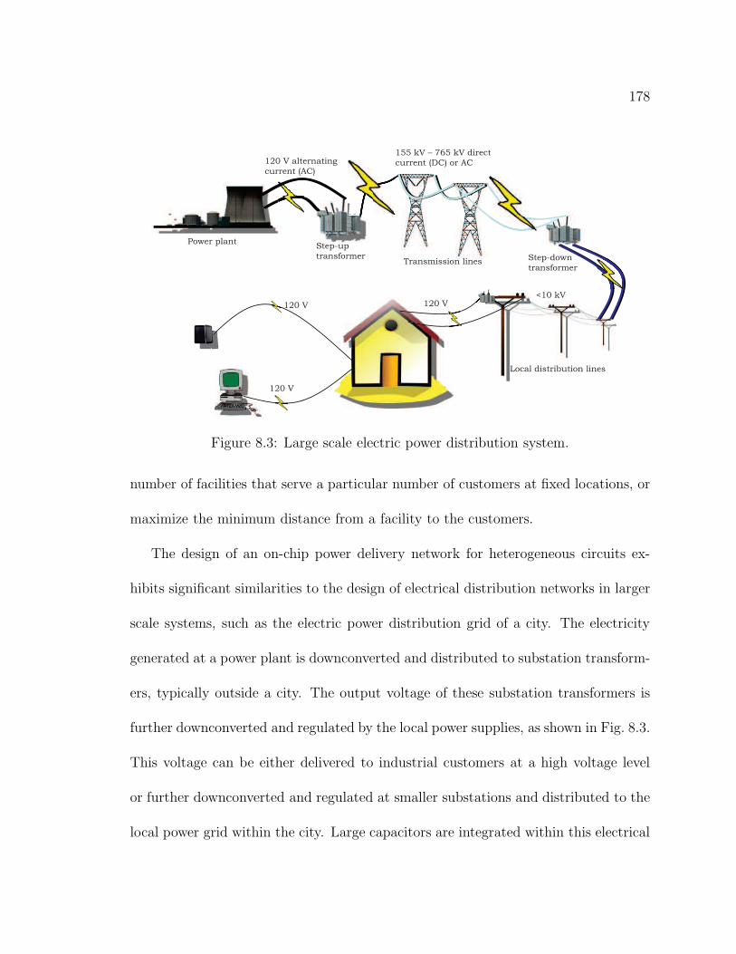
178
Step-up
transformer Step-down
transformerTransmission lines
Power plant
Local distribution lines
155 kV – 765 kV direct
current (DC) or AC
<10 kV
120 V alternating
current (AC)
120 V
120 V
120 V
Figure 8.3: Large scale electric power distribution system.
number of facilities that serve a particular number of customers at fixed locations, or
maximize the minimum distance from a facility to the customers.
The design of an on-chip power delivery network for heterogeneous circuits ex-
hibits significant similarities to the design of electrical distribution networks in larger
scale systems, such as the electric power distribution grid of a city. The electricity
generated at a power plant is downconverted and distributed to substation transform-
ers, typically outside a city. The output voltage of these substation transformers is
further downconverted and regulated by the local power supplies, as shown in Fig. 8.3.
This voltage can be either delivered to industrial customers at a high voltage level
or further downconverted and regulated at smaller substations and distributed to the
local power grid within the city. Large capacitors are integrated within this electrical

179
distribution system to reduce voltage fluctuations. Alternatively, in an integrated cir-
cuit, the board level voltage regulators downconvert the output voltage of the board
level power supply unit. This voltage is delivered to the on-chip voltage regulators or
directly to the on-chip power grid, which provides current to the load circuits. The re-
quired voltage levels and noise constraints are technology and design dependent. The
on-chip power delivery system is designed to deliver different voltage levels within
specified noise constraints. Decoupling capacitors are distributed throughout the on-
chip power delivery network to support the power distribution system by providing
local charge to the load circuits. A parallel can be drawn between the transformers
and off-chip voltage regulators, the small substations and on-chip voltage regulators,
and the large capacitors and on-chip decoupling capacitors. Additionally, the voltage
requirements within an integrated circuit vary in a similar manner as the voltage
requirements of different industrial and residential regions within a city.
Several optimization algorithms have been proposed to provide an optimal solution
to this problem. Due to the similarity between the electrical distribution network of
a city and the power distribution network of a heterogeneous circuit, analogous algo-
rithms can be applied to the design of these systems. Since facility location algorithms
are widely used to design electrical distribution networks [226, 227], these city plan-
ning algorithms are leveraged here in designing on-chip power networks within high
performance integrated circuits.

180
8.3 Proposed Optimization Methodology
The primary objective of the proposed optimization methodology is to determine
the optimal number and location of the on-chip power supplies and decoupling ca-
pacitors that minimize the maximum power noise and response time to certain blocks
while maintaining the area constant. Other design objectives can, however, be in-
corporated into the objective function while minimizing the maximum voltage drop
and response time for certain blocks, such as minimize the i) power consumed by the
power distribution networks, or ii) on-chip area.
A Euclidean or Manhattan distance is widely used in facility location problems
to determine a cost function. Alternatively, the cost of delivering power from a
power supply or a decoupling capacitor to a load circuit depends upon the parasitic
impedance of the power distribution network, the amount of current delivered to
the load circuit, and the parasitic impedance to the power supplies and decoupling
capacitors. A closed-form impedance model, proposed in [217], is utilized to determine
the effective impedance within the power grid from the power supplies and decoupling
capacitors to the load circuits. The physical distances and power grid characteristics
are included within this effective impedance model. Multiple power supplies and
decoupling capacitors can provide current to a single load circuit, depending upon
the physical distances among these components. The contribution from the power
supplies and decoupling capacitors to a load circuit is based on the requirements of

181
the load circuit. For example, when the current profile exhibits a fast transition time,
a decoupling capacitor is a better choice due to the faster response of these structures.
An objective function F (n,m, k) is proposed to determine the optimum location of
the power supplies and decoupling capacitors. F (n,m, k) is comprised of three terms.
Minimizing the first and second terms optimizes the location of the power sources for
minimum noise whereas minimizing the third term optimizes the locations to provide
a fast response to certain blocks. The solution of the weighted average of these three
terms provides the optimum location of the power sources for both minimum power
noise and fastest response.
Multiple parameters such as the parasitic impedance of the power network, output
impedance of the power supply, effective series resistance of a decoupling capacitor,
and load current characteristics significantly affect the power noise. These parameters
are therefore considered in the first and second terms of the optimization function
where the parasitic impedance of the power network is characterized by the closed-
form effective impedance model [217]. Alternatively, the response time of the power
delivery network to transient changes in the current within certain blocks is min-
imized by placing the decoupling capacitors physically close to these blocks. The
third term is therefore included within the objective function to place the decoupling
capacitors close to those circuit blocks demanding a fast transient current. The con-
tribution of the decoupling capacitor to the circuit blocks, the normalized transition
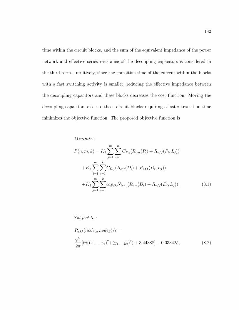
182
time within the circuit blocks, and the sum of the equivalent impedance of the power
network and effective series resistance of the decoupling capacitors is considered in
the third term. Intuitively, since the transition time of the current within the blocks
with a fast switching activity is smaller, reducing the effective impedance between
the decoupling capacitors and these blocks decreases the cost function. Moving the
decoupling capacitors close to those circuit blocks requiring a faster transition time
minimizes the objective function. The proposed objective function is
Minimize
F (n,m, k) = K1
m∑
j=1
n∑
i=1
CPij(Rout(Pi) +Reff(Pi, Lj))
+K2
m∑
j=1
k∑
i=1
CDij(Resr(Di) +Reff (Di, Lj))
+K3
m∑
j=1
k∑
i=1
capDiNtrLj
(Resr(Di) +Reff(Di, Lj)), (8.1)
Subject to :
Reff (nodeα, nodeβ)/r =√1
2π[ln((x1 − x2)
2+(y1 − y2)2) + 3.44388]− 0.033425, (8.2)
183
1 < xα,β < (Grid size)X , (8.3)
1 < yα,β < (Grid size)Y , (8.4)
m∑
j=1
CPij≤ capPi
, (8.5)
m∑
j=1
CDij≤ capDi
, (8.6)
n∑
i=1
CPij+
k∑
i=1
CDij=
m∑
i=1
Ii, (8.7)
n∑
i=1
capPi+
k∑
i=1
capDi≥
m∑
i=1
Ii, (8.8)
where the definition of the aforementioned parameters are listed in Table 8.1.
The maximum voltage drop and/or response time is minimized using the objec-
tive function F (n,m, k), where the effective resistance is defined in (8.2) [217]. By
applying constraints (8.3) and (8.4), the optimum location of the power supplies and
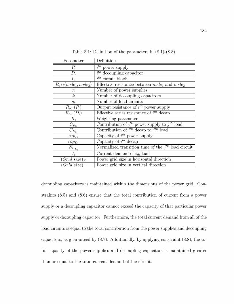
184
Table 8.1: Definition of the parameters in (8.1)-(8.8).
Parameter Definition
Pi ith power supplyDi ith decoupling capacitorLi ith circuit block
Reff(node1, node2) Effective resistance between node1 and node2n Number of power suppliesk Number of decoupling capacitorsm Number of load circuits
Rout(Pi) Output resistance of ith power supplyResr(Di) Effective series resistance of ith decap
Ki Weighting parameterCPij
Contribution of ith power supply to jth loadCDij
Contribution of ith decap to jth loadcapPi
Capacity of ith power supplycapDi
Capacity of ith decapNtrLj
Normalized transition time of the jth load circuit
Ii Current demand of ith load(Grid size)X Power grid size in horizontal direction(Grid size)Y Power grid size in vertical direction
decoupling capacitors is maintained within the dimensions of the power grid. Con-
straints (8.5) and (8.6) ensure that the total contribution of current from a power
supply or a decoupling capacitor cannot exceed the capacity of that particular power
supply or decoupling capacitor. Furthermore, the total current demand from all of the
load circuits is equal to the total contribution from the power supplies and decoupling
capacitors, as guaranteed by (8.7). Additionally, by applying constraint (8.8), the to-
tal capacity of the power supplies and decoupling capacitors is maintained greater
than or equal to the total current demand of the circuit.

185
In the proposed optimization function, Ki (see Table 8.1) provides the flexibility
to optimize the power distribution system for different objectives, such as minimizing
the maximum voltage drop or response time. When K3 (or K1 and K2) is equal
to zero, the location of the power supplies and decoupling capacitors is chosen to
minimize the maximum voltage drop (or response time). When the total capacity
of the available power supplies and decoupling capacitors is greater than the total
current demand of the integrated circuit, the current can be supplied either from the
decoupling capacitors or power supplies, which satisfies (8.8). For example, when
the physical area occupied by the power supplies and decoupling capacitors is not
the determining constraint but rather the total power consumption is the primary
bottleneck, adding more decoupling capacitors instead of on-chip power supplies is a
better option if the noise constraints are satisfied. In this case, K1 should be greater
than K2 to ensure that the weight of the first term in (8.1) (i.e., the cost function of
the power supplies) is greater than the weight of the second term in (8.1) (i.e., the
cost function of the decoupling capacitors). Ki can therefore be treated as a weighting
parameter to balance the optimization process for different design constraints.
8.4 Case Study and Benchmark Circuits
The optimum number and location of the power supplies and decoupling capac-
itors that minimize the voltage drop and response time within certain blocks are

186
determined for a small sample circuit, as shown in Fig. 8.4, to provide an intuitive
understanding of the proposed methodology. The sample circuit is composed of nine
circuit blocks with different current profiles. The third and seventh blocks have cur-
rent profiles with a faster transition time (i.e., 20 ps) than the rest of the circuits
which have a relatively slower transition time (i.e., 100 ps). Since the decoupling
capacitors provides immediate charge, intuitively, the decoupling capacitors should
be placed close to those blocks with a fast transition time to provide a fast response
to transient changes in the current. The optimum location of the power supplies
and decoupling capacitors that minimizes both the maximum voltage drop and re-
sponse time for certain blocks (the third and seventh blocks) is used, where K1, K2,
and K3 are set to one. The optimum location of one large on-chip power supply
and ten decoupling capacitors (case 1) is shown in Fig. 8.4a. The power supply is
located at a central location to reduce the maximum physical distance to each of
the circuit blocks. The decoupling capacitors, however, are placed physically close
to the third and seventh blocks. Most of the current demand of these blocks is pro-
vided by the surrounding decoupling capacitors. The optimum location of the four
relatively low current power supplies and 20 small decoupling capacitors (case 2) is
also determined, as shown in Fig. 8.4b. In this case, the third and seventh circuit
blocks are surrounded by local decoupling capacitors whereas the power supplies are

187
distributed to ensure that the maximum distance from the power supplies to the re-
maining blocks is minimized. The voltage drop map for these two cases is shown in
Fig. 8.5, where increasing the number of power supplies and decoupling capacitors
significantly reduces the voltage drop. The maximum voltage drop is 133 mV and
77 mV, respectively, for cases 1 and 2. More than a 40% reduction in the maximum
voltage drop is achieved by increasing the number and distributing the location of
the power supplies and decoupling capacitors.
The area of an on-chip power supply is typically dominated by the output pass
transistors [225], where the size of these pass transistors changes linearly with the
maximum output current demand. The size of an on-chip power supply therefore
changes linearly with the maximum output current capacity. Additionally, when
the on-chip power supplies are sufficiently small, the ultra-small power supplies are
combined to form a larger power supply with a higher output current. In this chapter,
the size of a power supply is assumed to change linearly with the maximum output
current capacity.
The optimal location of the power supplies and decoupling capacitors for sev-
eral ISPD’11 placement benchmark suite circuits is evaluated with the proposed dis-
tributed power delivery methodology for a different number of power supply and de-
coupling capacitor configurations [228]. The floorplan of these circuits is illustrated
in Fig. 8.6. More than 15,000 individual circuit blocks exist in these circuits. As
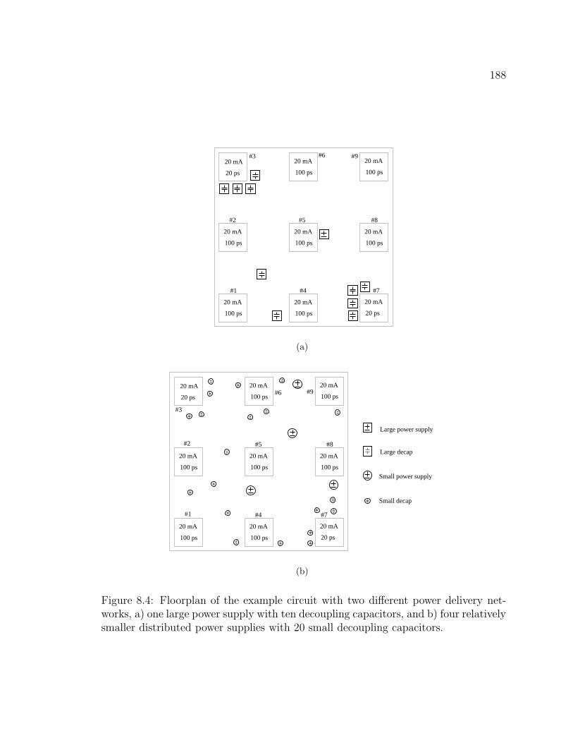
188
20 mA
20 ps
20 mA
20 ps
20 mA
100 ps
20 mA
100 ps
20 mA
100 ps
20 mA
100 ps
20 mA
100 ps
20 mA
100 ps
20 mA
100 ps
#2
#1
#3 #6
#5
#4 #7
#8
#9
(a)
20 mA
20 ps
20 mA
20 ps
20 mA
100 ps
20 mA
100 ps
20 mA
100 ps
20 mA
100 ps
20 mA
100 ps
20 mA
100 ps
20 mA
100 ps
Large power supply
Small power supply
Small decap
Large decap
#1
#2
#4
#5
#6
#7
#8
#9
#3
(b)
Figure 8.4: Floorplan of the example circuit with two different power delivery net-works, a) one large power supply with ten decoupling capacitors, and b) four relativelysmaller distributed power supplies with 20 small decoupling capacitors.
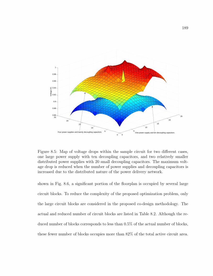
189
0
5
10
15
20
25
0
5
10
15
20
250.86
0.88
0.9
0.92
0.94
0.96
0.98
1
Vol
tage
(V
)
Four power supplies and twenty decoupling capacitors One power supply and ten decoupling capacitors
Figure 8.5: Map of voltage drops within the sample circuit for two different cases,one large power supply with ten decoupling capacitors, and two relatively smallerdistributed power supplies with 20 small decoupling capacitors. The maximum volt-age drop is reduced when the number of power supplies and decoupling capacitors isincreased due to the distributed nature of the power delivery network.
shown in Fig. 8.6, a significant portion of the floorplan is occupied by several large
circuit blocks. To reduce the complexity of the proposed optimization problem, only
the large circuit blocks are considered in the proposed co-design methodology. The
actual and reduced number of circuit blocks are listed in Table 8.2. Although the re-
duced number of blocks corresponds to less than 0.5% of the actual number of blocks,
these fewer number of blocks occupies more than 82% of the total active circuit area.
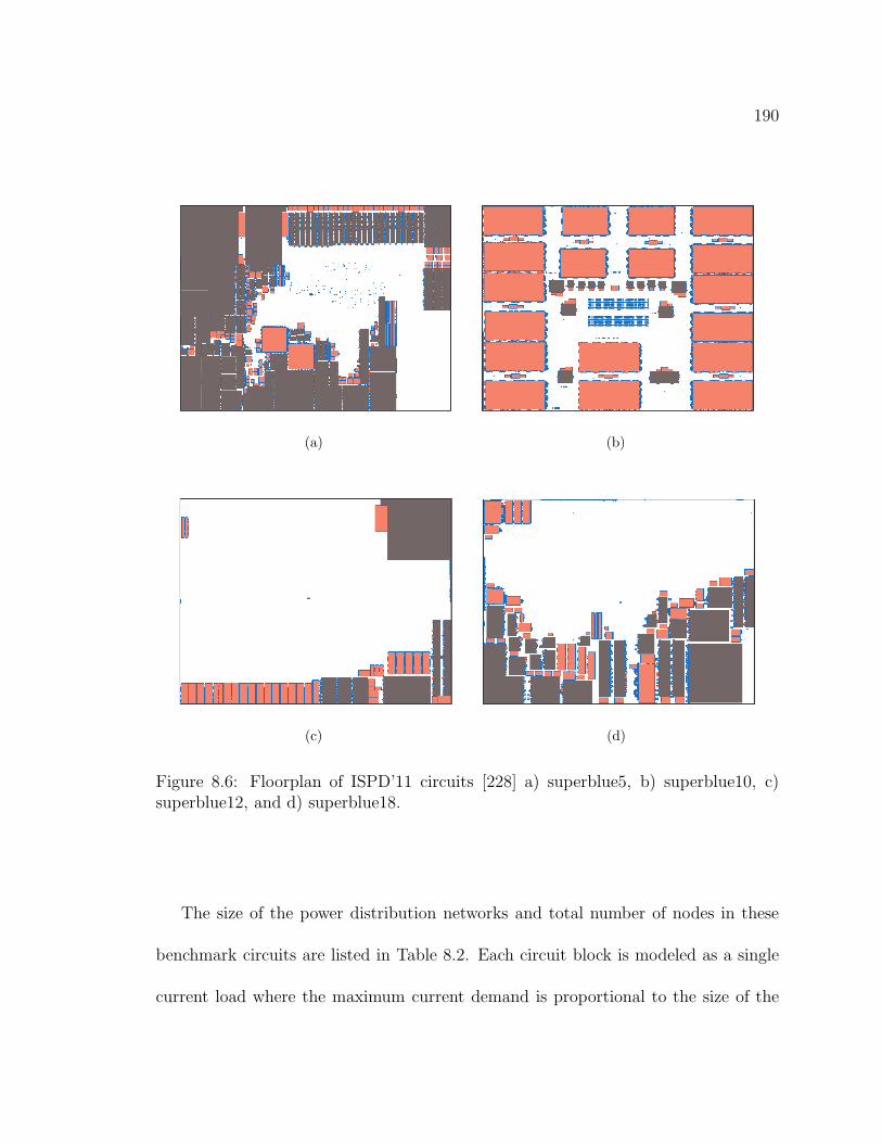
190
(a) (b)
(c) (d)
Figure 8.6: Floorplan of ISPD’11 circuits [228] a) superblue5, b) superblue10, c)superblue12, and d) superblue18.
The size of the power distribution networks and total number of nodes in these
benchmark circuits are listed in Table 8.2. Each circuit block is modeled as a single
current load where the maximum current demand is proportional to the size of the
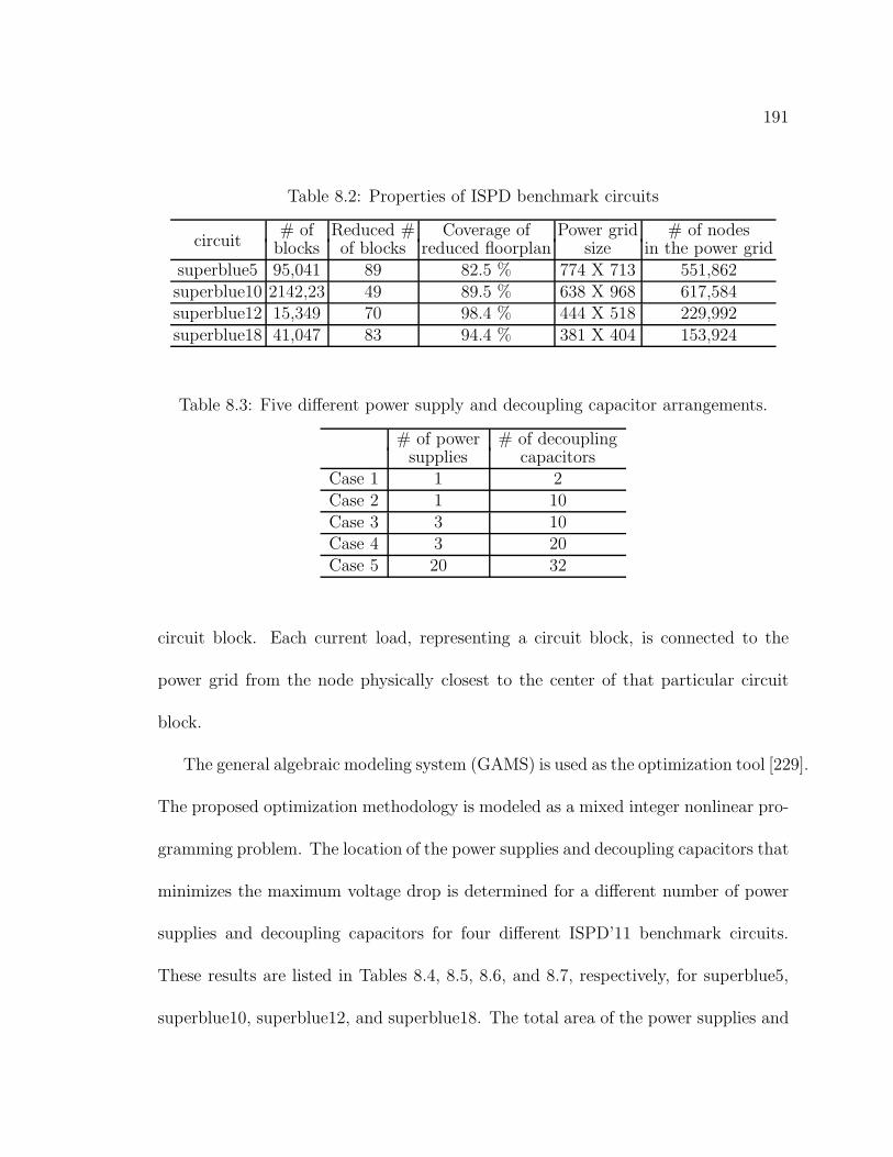
191
Table 8.2: Properties of ISPD benchmark circuits
circuit# of Reduced # Coverage of Power grid # of nodesblocks of blocks reduced floorplan size in the power grid
superblue5 95,041 89 82.5 % 774 X 713 551,862superblue10 2142,23 49 89.5 % 638 X 968 617,584superblue12 15,349 70 98.4 % 444 X 518 229,992superblue18 41,047 83 94.4 % 381 X 404 153,924
Table 8.3: Five different power supply and decoupling capacitor arrangements.
# of power # of decouplingsupplies capacitors
Case 1 1 2Case 2 1 10Case 3 3 10Case 4 3 20Case 5 20 32
circuit block. Each current load, representing a circuit block, is connected to the
power grid from the node physically closest to the center of that particular circuit
block.
The general algebraic modeling system (GAMS) is used as the optimization tool [229].
The proposed optimization methodology is modeled as a mixed integer nonlinear pro-
gramming problem. The location of the power supplies and decoupling capacitors that
minimizes the maximum voltage drop is determined for a different number of power
supplies and decoupling capacitors for four different ISPD’11 benchmark circuits.
These results are listed in Tables 8.4, 8.5, 8.6, and 8.7, respectively, for superblue5,
superblue10, superblue12, and superblue18. The total area of the power supplies and
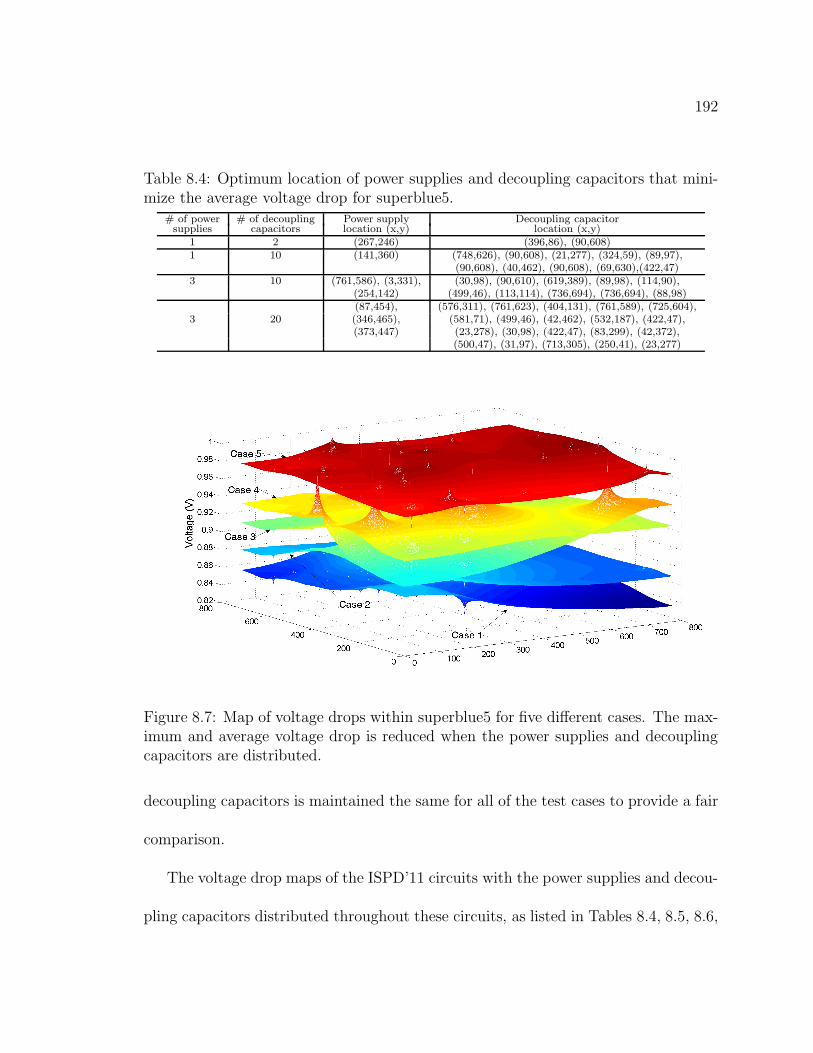
192
Table 8.4: Optimum location of power supplies and decoupling capacitors that mini-mize the average voltage drop for superblue5.
# of power # of decoupling Power supply Decoupling capacitorsupplies capacitors location (x,y) location (x,y)
1 2 (267,246) (396,86), (90,608)1 10 (141,360) (748,626), (90,608), (21,277), (324,59), (89,97),
(90,608), (40,462), (90,608), (69,630),(422,47)3 10 (761,586), (3,331), (30,98), (90,610), (619,389), (89,98), (114,90),
(254,142) (499,46), (113,114), (736,694), (736,694), (88,98)(87,454), (576,311), (761,623), (404,131), (761,589), (725,604),
3 20 (346,465), (581,71), (499,46), (42,462), (532,187), (422,47),(373,447) (23,278), (30,98), (422,47), (83,299), (42,372),
(500,47), (31,97), (713,305), (250,41), (23,277)
Figure 8.7: Map of voltage drops within superblue5 for five different cases. The max-imum and average voltage drop is reduced when the power supplies and decouplingcapacitors are distributed.
decoupling capacitors is maintained the same for all of the test cases to provide a fair
comparison.
The voltage drop maps of the ISPD’11 circuits with the power supplies and decou-
pling capacitors distributed throughout these circuits, as listed in Tables 8.4, 8.5, 8.6,
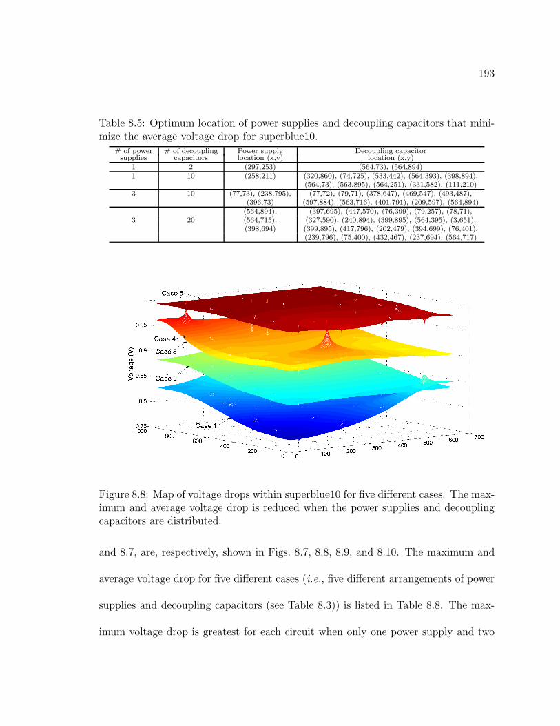
193
Table 8.5: Optimum location of power supplies and decoupling capacitors that mini-mize the average voltage drop for superblue10.
# of power # of decoupling Power supply Decoupling capacitorsupplies capacitors location (x,y) location (x,y)
1 2 (297,253) (564,73), (564,894)1 10 (258,211) (320,860), (74,725), (533,442), (564,393), (398,894),
(564,73), (563,895), (564,251), (331,582), (111,210)3 10 (77,73), (238,795), (77,72), (79,71), (378,647), (469,547), (493,487),
(396,73) (597,884), (563,716), (401,791), (209,597), (564,894)(564,894), (397,695), (447,570), (76,399), (79,257), (78,71),
3 20 (564,715), (327,590), (240,894), (399,895), (564,395), (3,651),(398,694) (399,895), (417,796), (202,479), (394,699), (76,401),
(239,796), (75,400), (432,467), (237,694), (564,717)
Figure 8.8: Map of voltage drops within superblue10 for five different cases. The max-imum and average voltage drop is reduced when the power supplies and decouplingcapacitors are distributed.
and 8.7, are, respectively, shown in Figs. 8.7, 8.8, 8.9, and 8.10. The maximum and
average voltage drop for five different cases (i.e., five different arrangements of power
supplies and decoupling capacitors (see Table 8.3)) is listed in Table 8.8. The max-
imum voltage drop is greatest for each circuit when only one power supply and two
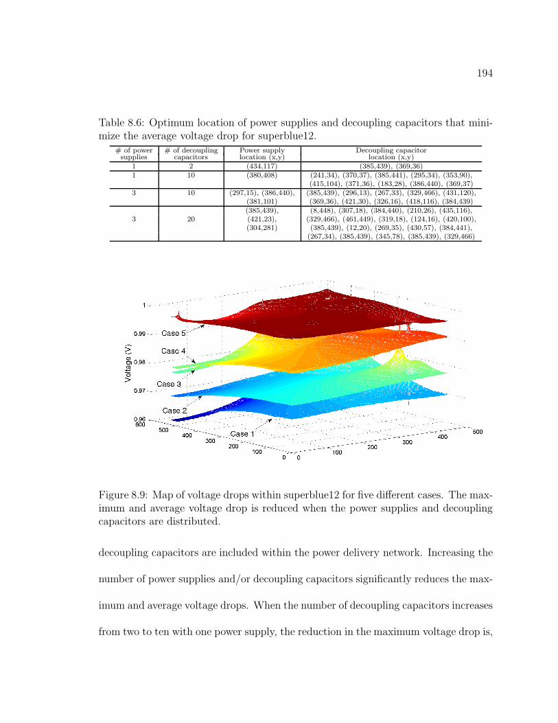
194
Table 8.6: Optimum location of power supplies and decoupling capacitors that mini-mize the average voltage drop for superblue12.
# of power # of decoupling Power supply Decoupling capacitorsupplies capacitors location (x,y) location (x,y)
1 2 (434,117) (385,439), (369,36)1 10 (380,408) (241,34), (370,37), (385,441), (295,34), (353,90),
(415,104), (371,36), (183,28), (386,440), (369,37)3 10 (297,15), (386,440), (385,439), (296,13), (267,33), (329,466), (431,120),
(381,101) (369,36), (421,30), (326,16), (418,116), (384,439)(385,439), (8,448), (307,18), (384,440), (210,26), (435,116),
3 20 (421,23), (329,466), (461,449), (319,18), (124,16), (420,100),(304,281) (385,439), (12,20), (269,35), (430,57), (384,441),
(267,34), (385,439), (345,78), (385,439), (329,466)
Figure 8.9: Map of voltage drops within superblue12 for five different cases. The max-imum and average voltage drop is reduced when the power supplies and decouplingcapacitors are distributed.
decoupling capacitors are included within the power delivery network. Increasing the
number of power supplies and/or decoupling capacitors significantly reduces the max-
imum and average voltage drops. When the number of decoupling capacitors increases
from two to ten with one power supply, the reduction in the maximum voltage drop is,
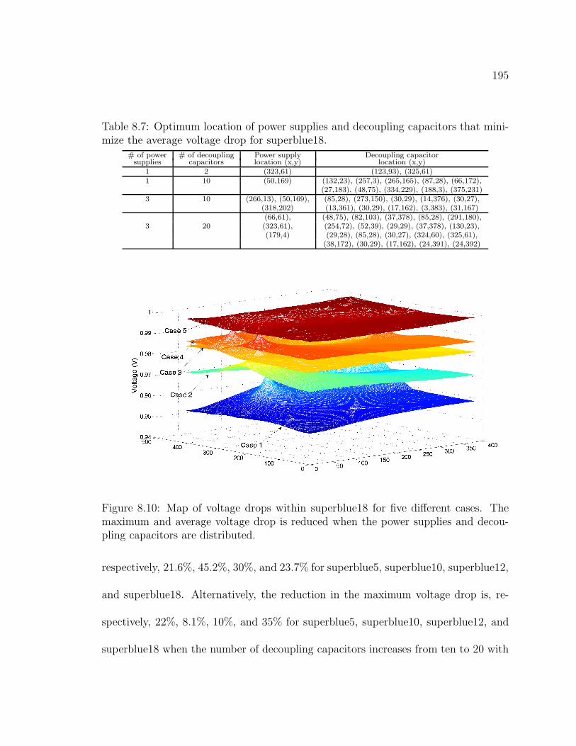
195
Table 8.7: Optimum location of power supplies and decoupling capacitors that mini-mize the average voltage drop for superblue18.
# of power # of decoupling Power supply Decoupling capacitorsupplies capacitors location (x,y) location (x,y)
1 2 (323,61) (123,93), (325,61)1 10 (50,169) (132,23), (257,3), (265,165), (87,28), (66,172),
(27,183), (48,75), (334,229), (188,3), (375,231)3 10 (266,13), (50,169), (85,28), (273,150), (30,29), (14,376), (30,27),
(318,202) (13,361), (30,29), (17,162), (3,383), (31,167)(66,61), (48,75), (82,103), (37,378), (85,28), (291,180),
3 20 (323,61), (254,72), (52,39), (29,29), (37,378), (130,23),(179,4) (29,28), (85,28), (30,27), (324,60), (325,61),
(38,172), (30,29), (17,162), (24,391), (24,392)
Figure 8.10: Map of voltage drops within superblue18 for five different cases. Themaximum and average voltage drop is reduced when the power supplies and decou-pling capacitors are distributed.
respectively, 21.6%, 45.2%, 30%, and 23.7% for superblue5, superblue10, superblue12,
and superblue18. Alternatively, the reduction in the maximum voltage drop is, re-
spectively, 22%, 8.1%, 10%, and 35% for superblue5, superblue10, superblue12, and
superblue18 when the number of decoupling capacitors increases from ten to 20 with

196
three power supplies.
The average voltage drop throughout the power distribution networks for different
cases is also listed in Table 8.8. When the number of power supplies and decoupling
capacitors increases, the power sources can be locally distributed throughout the
large power distribution network, providing local current to the load circuits. Both
the maximum and average power noise is therefore significantly reduced for different
circuits with diverse floorplans.
8.5 Discussion
With the introduction of ultra-small on-chip voltage regulators [60,225], the num-
ber of voltage regulators on a single die will increase significantly to maintain the
increasingly stringent noise constraints in sub-20 nm integrated circuits. Delivering
a robust power supply voltage to circuits with varying noise and voltage constraints
is crucial to maintaining the performance of next generation integrated circuits. Lo-
cal supply voltages are generated and regulated by point-of-load voltage regulators
within a distributed power delivery system. Since the physical distance among the
power sources and load circuits is less with a distributed power delivery system, the
inductive L di/dt and resistive IR power noise is reduced, since the power source is
placed physically closer to the load circuits.
In the proposed optimization methodology, minimizing the maximum voltage drop
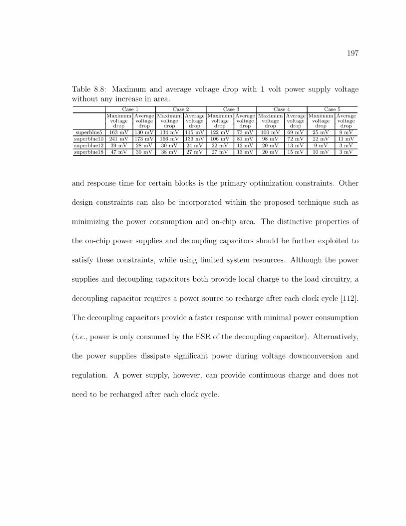
197
Table 8.8: Maximum and average voltage drop with 1 volt power supply voltagewithout any increase in area.
Case 1 Case 2 Case 3 Case 4 Case 5Maximum Average Maximum Average Maximum Average Maximum Average Maximum Averagevoltage voltage voltage voltage voltage voltage voltage voltage voltage voltagedrop drop drop drop drop drop drop drop drop drop
superblue5 163 mV 130 mV 134 mV 115 mV 122 mV 73 mV 100 mV 69 mV 25 mV 9 mVsuperblue10 241 mV 173 mV 166 mV 133 mV 106 mV 81 mV 98 mV 72 mV 22 mV 11 mVsuperblue12 39 mV 28 mV 30 mV 24 mV 22 mV 12 mV 20 mV 13 mV 9 mV 3 mVsuperblue18 47 mV 39 mV 38 mV 27 mV 27 mV 13 mV 20 mV 15 mV 10 mV 3 mV
and response time for certain blocks is the primary optimization constraints. Other
design constraints can also be incorporated within the proposed technique such as
minimizing the power consumption and on-chip area. The distinctive properties of
the on-chip power supplies and decoupling capacitors should be further exploited to
satisfy these constraints, while using limited system resources. Although the power
supplies and decoupling capacitors both provide local charge to the load circuitry, a
decoupling capacitor requires a power source to recharge after each clock cycle [112].
The decoupling capacitors provide a faster response with minimal power consumption
(i.e., power is only consumed by the ESR of the decoupling capacitor). Alternatively,
the power supplies dissipate significant power during voltage downconversion and
regulation. A power supply, however, can provide continuous charge and does not
need to be recharged after each clock cycle.
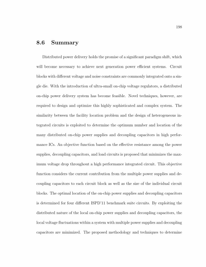
198
8.6 Summary
Distributed power delivery holds the promise of a significant paradigm shift, which
will become necessary to achieve next generation power efficient systems. Circuit
blocks with different voltage and noise constraints are commonly integrated onto a sin-
gle die. With the introduction of ultra-small on-chip voltage regulators, a distributed
on-chip power delivery system has become feasible. Novel techniques, however, are
required to design and optimize this highly sophisticated and complex system. The
similarity between the facility location problem and the design of heterogeneous in-
tegrated circuits is exploited to determine the optimum number and location of the
many distributed on-chip power supplies and decoupling capacitors in high perfor-
mance ICs. An objective function based on the effective resistance among the power
supplies, decoupling capacitors, and load circuits is proposed that minimizes the max-
imum voltage drop throughout a high performance integrated circuit. This objective
function considers the current contribution from the multiple power supplies and de-
coupling capacitors to each circuit block as well as the size of the individual circuit
blocks. The optimal location of the on-chip power supplies and decoupling capacitors
is determined for four different ISPD’11 benchmark suite circuits. By exploiting the
distributed nature of the local on-chip power supplies and decoupling capacitors, the
local voltage fluctuations within a system with multiple power supplies and decoupling
capacitors are minimized. The proposed methodology and techniques to determine

199
the optimum location of the local power supplies and decoupling capacitors provides
a means to realize more robust and efficient power delivery systems.

200
Chapter 9
Future Work
As described in previous chapters, power delivery in high performance integrated
circuits is a challenging process. Advancements in semiconductor technology over the
past several decades exacerbate the requirements of power delivery networks to satisfy
extreme performance constraints. Fueling this growth is the demand for greater func-
tionality within a single device that can deliver ever increasing levels of performance
under a tight power budget. Each component within these highly sophisticated sys-
tems requires power to operate, and the performance of the system depends strongly
on the quality of the voltage delivered to the circuits. An effective power delivery
system is needed to provide a high quality supply voltage from the voltage generator
to the billions of load circuits. Additionally, power consumption is now a significant
issue with the proliferation of battery powered mobile devices. The need for greater
functionality within a small form factor requires scaling without higher leakage power,
which demands a unified circuit design methodology and power management strategy

201
to develop these highly complex power delivery systems.
Three different research problems based on previously discussed topics presented
in this dissertation are proposed in this chapter for further investigation. An effective
impedance model that considers inductors and capacitors is discussed in Section 9.1.
A power grid analysis algorithm to analyze transient voltage fluctuations is proposed
in Section 9.2. In Section 9.3, a simultaneous co-design methodology for power and
clock distribution networks is described. A summary is offered in Section 9.4.
9.1 Effective Impedance within a Power Grid
A model of the effective resistance is generally used during the design and analysis
of power delivery networks, as described in Chapter 5. Although effective resistance
models are widely used to enhance the computational efficiency of the static power
grid analysis process, the on-chip inductance and capacitance should also be con-
sidered to analyze transient voltage fluctuations. Closed-form expressions for the
effective impedance can significantly speed up the transient power grid analysis pro-
cess.
The self-inductance is typically modeled in series with the on-chip resistance as
shown in Fig. 9.1. Adding the self-inductance to the effective resistance model to de-
termine the effective impedance is a straightforward process. Alternatively, determin-
ing the effective impedance becomes exceedingly more complicated when capacitors
202
Decoupling capacitor
Self−inductance
Resistance
Figure 9.1: Power grid model for transient analysis. Parasitic inductance of the powergrid is modeled in series with the parasitic resistance.
are included in the effective impedance model. The capacitors can be modeled as an
impedance where the complex impedance is a function of the frequency of operation,
which depends upon the transition time of the current drawn by the load circuits.
Novel analytic techniques need to be developed since adding capacitors and inductors
to the power grid model affects the symmetric nature of the network.
203
9.2 Transient Power Grid Analysis Based on Closed-
Form Expressions
The effects of the capacitors, inductors, and time varying current waveforms are
neglected in static IR voltage drop analysis. Although static voltage drop analy-
sis is used to determine the steady state node voltages, efficient power grid analysis
techniques are needed to determine the time varying node voltages that consider the
effects of the on-chip capacitors, inductors, and time varying current waveforms at
the load. Effective impedance models that consider capacitors and inductors will
enhance the efficiency of the power grid analysis process. The effective impedance of
a power network determined at a specific frequency can be used to analyze the fre-
quency response of a system to abrupt changes in the current load demand. Pre- and
post-layout full IC simulation of modern microprocessors requires infeasible computa-
tional time due to the significant size of the interrelated system. Power grid analysis
techniques based on closed-form expressions significantly reduces the computational
runtime and memory requirements, thereby enabling the efficient simulation of power
grids with over 100 million nodes.

204
9.3 Power and Clock Network Co-Design
Variations in the power supply affect the data path delay by changing the supply
voltage during a switching event. The DC component of the voltage drop results in
a constant clock skew while the time varying components produce clock jitter and
delay uncertainty. Alternatively, clock skew can be scheduled to dramatically lower
the power supply noise by spreading the voltage drop over time [230]. Traditionally,
power and clock networks are designed independently or, at best, in a loosely related
manner. These two networks, however, are intimately related and strong feedback is
formed among the power supply, clock skew, and logic gates. A co-design methodology
is required to address these issues of power, clock, and signal integrity, clock skew
management, and clock and data signal uncertainty. These interactions within a
power delivery system should be exploited and interdependencies among the clock
and power networks should be characterized. Identifying these interdependencies
and interactions will reduce on-chip noise, which will likely delay the need for more
advanced and expensive technologies to achieve the same performance and function.

205
9.4 Summary
The importance of accurate modeling, efficient analysis, and effective design of
power delivery systems has significantly increased over the past decade with the pro-
liferation of low power mobile devices that operate on batteries. Several topics have
been suggested for future research that address some of these issues in the design of
high performance power delivery systems.
The importance of an effective impedance model to develop efficient power grid
analysis techniques targeting transient voltage fluctuations has been discussed. A
methodology to simultaneously co-design power and clock networks that improves
the signal and power integrity of high performance circuits has been proposed.

206
Chapter 10
Conclusions
Every complex system is composed of small components, typically with simple
structures capable of providing a wide variety of functions. The interactions and ag-
gregation of these components form a highly complex system. The performance of an
integrated circuit – one of the most complicated systems ever manufactured by hu-
mankind – depends strongly upon both the efficient design and effective management
of the individual components within the system as well as the effective control of the
multitude of interactions among these components. A common underlying principle
of all of these small components is that each component in the vast sea of components
within an IC requires a clean supply voltage to operate correctly. The performance
of a power delivery system is particularly governed by the i) power supply, ii) inter-
connection network within the power delivery system, and iii) algorithms to analyze
on-chip power integrity. In this dissertation, circuit design techniques, methodologies,
and algorithms at multiple levels of abstraction have been proposed to deliver a high
207
quality supply voltage to the billions of loads.
Placing multiple point-of-load on-chip power supplies is challenging since the area
occupied by a single power supply should be small and the power efficiency sufficiently
high. Existing on-chip power supply topologies do not simultaneously satisfy these
two requirements. Accordingly, a hybrid combination of a switching and low dropout
(LDO) regulator as a point-of-load power supply for next generation heterogeneous
systems has been proposed. The key concept in developing this ultra-small on-chip
power supply is to replace the passive LC filter within the buck converter with a
more area efficient active filter since the area occupied by a passive LC filter is a
primary issue in the design of a monolithic buck converter. This voltage regulator
has been successfully designed and manufactured in a commercial 110 nm TSMC
CMOS technology. Despite the mature 110 nm technology, the total on-chip area is
approximately 0.015 mm2, which is significantly smaller than state-of-the-art on-chip
voltage regulators. This ultra-small voltage regulator is appropriate for on-chip point-
of-load voltage regulation with hundreds of power regulators distributed throughout
an integrated circuit to facilitate dynamic voltage and frequency scaling (DVFS).
An important challenge in the realization of efficient power delivery systems is the
analysis of this highly complicated structure where individual voltage fluctuations
at many millions of nodes need to be determined. The parasitic impedance of the
interconnects, decoupling capacitances, load circuits, and on-chip power regulators are
208
computationally expensive to simultaneously analyze. The distinctive properties of a
power network have been exploited to develop closed-form expressions for the effective
resistance between circuit components. The effective resistance model is based on
the physical distance between circuit components within a two layer mesh where
the horizontal and vertical unit resistances may be different. This effective resistance
model is utilized in the development of a power grid analysis algorithm to compute the
node voltage without requiring any iterations. This algorithm drastically improves
computational complexity since the iterative procedures commonly used today to
determine IR drop and L di/dt noise are no longer needed. The symmetric nature of
the power and ground distribution networks and the principle of spatial locality are
also exploited to further enhance the computational efficiency and accuracy of the
analysis process.
Power and ground (P/G) networks are often used as shield lines to mitigate cou-
pling noise by electrically isolating the aggressor and victim lines. These shield lines
are typically treated as ideal noise free lines, which do not accurately model the effect
of noise on the shield line. Since the distance between the shield and victim lines
is smaller than the distance between the aggressor and victim lines, P/G noise on
the shield line can produce greater noise on the victim line than the crosstalk noise
coupled from the aggressor to the victim. Hence, while a shield line reduces noise
209
coupling from the aggressor interconnect, the shield line can also increase noise cou-
pling due to P/G noise. The detrimental effects of P/G noise on the efficacy of an
important noise reduction technique, shield insertion, to reduce noise coupling from
the aggressor to the victim lines have also been investigated. In this dissertation, the
effectiveness of physical spacing and shield insertion in terms of the coupling noise
on the victim line for several technology nodes has been evaluated. Boundary condi-
tions are provided to determine the effective range of spacing and shield insertion in
the presence of P/G noise. The effects of technology scaling on P/G noise, shielding
efficiency, and related design tradeoffs have also been addressed.
The design of on-chip power distribution networks has become more challenging
with the introduction of on-chip point-of-load voltage regulators. The optimal lo-
cation of the power supplies and decoupling capacitors needs to be determined to
reduce power/ground noise while minimizing on-chip area and power consumption.
Optimization algorithms widely used for facility location problems have been applied
to determine the optimal number and location of the power supplies and decoupling
capacitors. An objective function based on the effective resistance among the power
supplies, decoupling capacitors, and load circuits is proposed that minimizes the max-
imum voltage drop throughout a heterogeneous integrated circuit. The effects of the
size, number, and location of the power supplies and decoupling capacitors on the
power noise have also been discussed.

210
The development of these new capabilities will fundamentally change the manner
in which power is delivered, producing a more efficient methodology for generating,
managing, and distributing power to the billions of components within a complex,
high performance integrated circuit. As opposed to conventional practices where the
power distribution network is designed first, followed by the placement of the decou-
pling capacitors, the proposed power grid models, voltage regulators, and co-design
methodologies enable a unified design process where locally distributed voltages are
generated close to the load using the proposed ultra-small voltage regulator, and the
signal integrity of the system is enhanced with the proposed co-design methodology
for delivering power. Ultimately, the proposed models, circuits, and design method-
ologies can become integral components of a power management scheme where the
individual voltage domains within different circuit blocks are finely tuned.

211
Bibliography
[1] J. E. Lilienfeld, Method and Apparatus for Controlling Electric Currents, U.S.
Patent No. 1,745,175, October 1926.
[2] B. Razavi, Design of Analog CMOS Integrated Circuits, New York: McGraw-
Hill, 2001.
[3] J. Bardeen and W. H. Brattain, “The Transistor, a Semi-Conductor Triode,”
Physics Review, Vol. 74, No. 2, pp. 230–231, July 1948.
[4] W. F. Brinkman, D. E. Haggan, and W. W. Troutman, “A History of the
Invention of the Transistor and Where It Will Lead Us,” IEEE Journal of
Solid-State Circuits, Vol. 32, No. 12, pp. 1858–1865, December 1997.
[5] R. G. Arns, “The Other Transistor: Early History of the Metal-Oxide Semi-
conductor Field-Effect Transistor,” Engineering Science and Education Journal,
Vol. 7, No. 5, pp. 233–240, October 1998.
[6] D. Kahng and M. M. Atalla, “Silicon - Silicon Dioxide Field Induced Surface
Devices,” presented at IRE - AIEE Solid - State Device Research Conference,
June 1960.
[7] F. M. Wanlass and C. T. Sah, “Nanowatt Logic Using Field-Effect Metal-Oxide
Semiconductor Triodes,” Proceedings of the IEEE International Solid-State
Circuits Conference, pp. 32–33, February 1963.
[8] G. E. Moore, “Cramming More Components onto Integrated Circuits,” Elec-
tronics Magazine, Vol. 38, No. 8, pp. 114–117, April 1965.
212
[9] S. Rusu et al., “A 45 nm 8-Core Enterprise Xeon Processor,” IEEE Journal of
Solid-State Circuits, Vol. 45, No. 1, pp. 7–14, January 2010.
[10] H. H. Chen and D. D. Ling, “Power Supply Noise Analysis Methodology for
Deep-Submicron VLSI Chip Design,” Proceedings of the IEEE/ACM Design
Automation Conference, pp. 638–643, June 1997.
[11] K. T. Tang and E. G. Friedman, “Transient IR Voltage Drops in CMOS-Based
Power Distribution Networks,” Proceedings of the IEEE Midwest Symposium
on Circuits and Systems, pp. 1396–1399, August 2000.
[12] A. H. Ajami, K. Banerjee, A. Mehrotra, and M. Pedram, “Analysis of IR-
Drop Scaling with Implications for Deep Submicron P/G Network Designs,”
Proceedings of the IEEE International Symposium on Quality Electronic Design,
pp. 35–40, March 2003.
[13] R. Jakushokas, M. Popovich, A. V. Mezhiba, S. Kose, and E. G. Friedman,
Power Distribution Networks with On-Chip Decoupling Capacitors, Second Edi-
tion, Springer, 2011.
[14] P. Larsson, “di/dt Noise in CMOS Integrated Circuits,” Analog Integrated
Circuits and Signal Processing, Vol. 14, No. 2, pp. 113–129, September 1997.
[15] Y.-S. Chang, S. K. Gupta, and M. A. Breuer, “Analysis of Ground Bounce in
Deep Sub-Micron Circuits,” Proceedings of the IEEE VLSI Test Symposium,
pp. 110–116, April/May 1997.
[16] K. T. Tang and E. G. Friedman, “Simultaneous Switching Noise in On-Chip
CMOS Power Distribution Networks,” IEEE Transactions on Very Large Scale
Integration (VLSI) Circuits, Vol. 10, No. 4, pp. 487–493, August 2002.
[17] M. K. Gowan, L. L. Biro, and D. B. Jackson, “Power Considerations in the
Design of the Alpha 21264 Microprocessor,” Proceedings of the IEEE/ACM
Design Automation Conference, pp. 726–731, June 1998.
213
[18] V. Kursun, S. G. Narendra, V. K. De, and E. G. Friedman, “Analysis of Buck
Converters for On-Chip Integration With a Dual Supply Voltage Microproces-
sor,” IEEE Transactions on Very Large Scale Integration (VLSI) Circuits, Vol.
11, No. 3, pp. 514–522, June 2003.
[19] R. Mahajan, V. Brown, and K. Atluri, “The Evolution of Microprocessor Pack-
aging,” Intel Technology Journal, Vol. Q3, pp. 1–10, 2000.
[20] S. Borkar, “Design Challenges of Technology Scaling,” IEEE Micro, Vol. 19,
No. 4, pp. 23–29, 1999.
[21] S. Borkar, “Obeying Moore’s Law Beyond 0.18 Micron,” Proceedings of the
ASIC/SOC Conference, pp. 26–31, September 2000.
[22] V. Kursun and E. G. Friedman, Multi-Voltage CMOS Circuit Design, Wiley &
Sons, 2006.
[23] S. Rusu et al., “A 65-nm Dual-Core Multithreaded Xeon Processor with 16-MB
L3 Cache,” IEEE Journal of Solid-State Circuits, Vol. 42, No. 1, pp. 17–25,
January 2007.
[24] P. Hazucha et al., “Area-Efficient Linear Regulator with Ultra-Fast Load Reg-
ulation,” IEEE Journal of Solid-State Circuits, Vol. 40, No. 4, pp. 933–940,
April 2005.
[25] W. Kim, M. S. Gupta, G.-Y. Wei, and D. Brooks, “System Level Analysis of
Fast, Per-Core DVFS Using On-Chip Switching Regulators,” Proceedings of the
IEEE International Symposium on High Performance Computer Architecture,
pp. 123–134, February 2008.
[26] G. A. Rincon-Mora and P. E. Allen, “A Low-Voltage, Low Quiescent Current,
Low Drop-Out Regulator,” IEEE Journal of Solid-State Circuits, Vol. 33, No.
1, pp. 36–44, January 1998.
[27] M. Ang, R. Salem, and A. Taylor, “An On-Chip Voltage Regulator Using
Switched Decoupling Capacitors,” Proceedings of the IEEE International Solid-
State Circuits Conference, pp. 438–439, February 2000.
214
[28] K. N. Leung and P. K. T. Mok, “A Capacitor-Free CMOS Low-Dropout Regu-
lator with Damping-Factor-Control Frequency Compensation,” IEEE Journal
of Solid-State Circuits, Vol. 38, No. 10, pp. 1691–1702, October 2003.
[29] R. J. Milliken, J. S.-Martinez, and E. S.-Sinencio, “Full On-Chip CMOS Low-
Dropout Voltage Regulator,” IEEE Transactions on Circuits and Systems I:
Regular Papers, Vol. 54, No. 9, pp. 1879–1890, September 2007.
[30] Y. Ramadass, A. Fayed, B. Haroun, and A. Chandrakasan, “A 0.16mm2 Com-
pletely On-Chip Switched-Capacitor DC-DC Converter Using Digital Capac-
itance Modulation for LDO Replacement in 45nm CMOS,” Proceedings of
the IEEE International Solid-State Circuits Conference, pp. 208–209, Febru-
ary 2010.
[31] H.-P. Le et al., “A 32 nm Fully Integrated Reconfigurable Switched-Capacitor
DC-DC Converter Delivering 0.55W/mm2 at 81% Efficiency,” Proceedings of
the IEEE International Solid-State Circuits Conference, pp. 210–211, February
2010.
[32] A. Roy, J. Xu, and M. H. Chowdhury, “Analysis of the Impacts of Signal Slew
and Skew on the Behavior of Coupled RLC Interconnects for Different Switching
Patterns,” IEEE Transactions on Very Large Scale Integration (VLSI) Circuits,
Vol. 18, No. 2, pp. 338–342, February 2010.
[33] Intel Corporation, 4004: Single Chip 4-Bit P-Channel Microprocessor, March
1987.
[34] Intel Corporation, Intel Core i7-900 Desktop Processor Extreme Edition Series
on 32-nm Process, July 2010.
[35] Intel Corporation, 8008: 8-Bit Parallel Central Processor Unit, November 1972.
[36] Intel Corporation, 8080A/8080A-1/8080A-2: 8-Bit N-Channel Microprocessor,
November 1986.
[37] Intel Corporation, 8085AH/8085AH-2/8085AH-1: 8-Bit HMOS Microproces-
sors, September 1987.
215
[38] Intel Corporation, 8086: 16-Bit HMOS Microprocessors, September 1990.
[39] Intel Corporation, 80C286/883: High Performance Microprocessor with Mem-
ory Management and Protection, September 1988.
[40] Intel Corporation, Intel386 EX Embedded Microprocessor, October 1998.
[41] Intel Corporation, Embedded Intel486 SX Processor, August 2004.
[42] Intel Corporation, Pentium Processor at iCOMP Intex 610-75MHz, June 1997.
[43] Intel Corporation, Pentium Pro Processor with 1 MB L2 Cache at 200 MHz,
January 1998.
[44] Intel Corporation, Pentium II Processor at 233MHz, 266MHz, 300MHz and
333MHz, January 1998.
[45] Intel Corporation, Pentium III Processor for the SC242 at 450MHz to 1.0GHz,
July 2002.
[46] Intel Corporation, Pentium IV Processor in the 423-Pin Package at 1.30, 1.40,
1.50, 1.60, 1.70, 1.80, 1.90, 2GHz, August 2001.
[47] Intel Corporation, Pentium IV Processor on 90nm Process, February 2005.
[48] T. Lopez, R. Elferich, and E. Alarcon, Voltage Regulators for Next Generation
Microprocessors, Springer, 2010.
[49] R. J. Widlar, “New Developments in IC Voltage Regulators,” IEEE Journal of
Solid-State Circuits, Vol. 6, No. 1, pp. 2–7, February 1971.
[50] G. A. Rincon-Mora, Current Efficient, Low Voltage, Low Dropout Regulators,
Ph.D. Thesis, Georgia Institute of Technology, November 1996.
[51] G. A. Rincon-Mora, Analog IC Design with Low-Dropout Regulators, McGraw-
Hill, 2009.
[52] M. M. Cirovic, Integrated Circuits: A User’s Handbook, Reston Publication
Company, 1977.
216
[53] C. K. Chava and J. Silva-Martinez, “A Frequency Compensation Scheme for
LDO Voltage Regulators,” IEEE Transactions on Circuits and Systems I: Reg-
ular Papers, Vol. 51, No. 6, pp. 1041–1050, June 2004.
[54] M. Al-Shyoukh, H. Lee, and R. Perez, “A Transient-Enhanced Low-Quiescent
Current Low-Dropout Regulator with Buffer Impedance Attenuation,” IEEE
Journal of Solid-State Circuits, Vol. 42, No. 8, pp. 1732–1742, August 2007.
[55] P. Y. Or and K. N. Leung, “A Fast-Transient Low-Dropout Regulator With
Load-Tracking Impedance Adjustment and Loop-Gain Boosting Technique,”
IEEE Transactions on Circuits and Systems II: Express Briefs, Vol. 57, No. 10,
pp. 757–761, October 2010.
[56] T. Y. Man, P. K. T. Mok, and M. Chan, “A High Slew-Rate Push-Pull Output
Amplifier for Low-Quiescent Current Low-Dropout Regulators with Transient-
Response Improvement,” IEEE Transactions on Circuits and Systems II: Ex-
press Briefs, Vol. 54, No. 9, pp. 755–759, September 2007.
[57] G. A. Rincon-Mora and P. E. Allen, “Optimized Frequency-Shaping Circuit
Topologies for LDOs,” IEEE Transactions on Circuits and Systems II: Analog
and Digital Signal Processing, Vol. 45, No. 6, pp. 703–708, June 1998.
[58] Y.-H. Lam and W.-H. Ki, “A 0.9 V 0.35 µm Adaptively Biased CMOS LDO
Regulator with Fast Transient Response,” Proceedings of the IEEE Interna-
tional Solid-State Circuits Conference, pp. 442–626, February 2008.
[59] P. Y. Or and K. N. Leung, “An Output-Capacitorless Low-Dropout Regulator
with Direct Voltage-Spike Detection,” IEEE Journal of Solid-State Circuits,
Vol. 45, No. 2, pp. 458–466, February 2010.
[60] J. Guo and K. N. Leung, “A 6-µW Chip-Area-Efficient Output-Capacitorless
LDO in 90-nm CMOS Technology,” IEEE Journal of Solid-State Circuits, Vol.
45, No. 9, pp. 1896–1905, September 2010.
[61] P. Hazucha et al., “A 233-MHz 80%-87% Efficient Four-Phase DC-DC Con-
verter Utilizing Air-Core Inductors on Package,” IEEE Journal of Solid-State
Circuits, Vol. 40, No. 4, pp. 838–845, April 2005.
217
[62] T. Y. Man, P. K. T. Mok, and M. Chan, “An Auto-Selectable-Frequency Pulse-
Width Modulator for Buck Converters with Improved Light-Load Efficiency,”
Proceedings of the IEEE International Solid-State Circuits Conference, pp. 440–
626, February 2008.
[63] M. Du and H. Lee, “An Integrated Speed- and Accuracy-Enhanced CMOS Cur-
rent Sensor With Dynamically Biased Shunt Feedback for Current-Mode Buck
Regulators,” IEEE Transactions on Circuits and Systems I: Regular Papers,
Vol. 57, No. 10, pp. 2804–2814, October 2010.
[64] A. Maity, A. Patra, N. Yamamura, and J. Knight, “Design of a 20 MHz DC-DC
Buck Converter with 84 Percent Efficiency for Portable Applications,” Pro-
ceedings of the IEEE International Conference on VLSI Design, pp. 316–321,
January 2011.
[65] S. Bandyopadhyay, Y. K. Ramadass, and A. P. Chandrakasan, “20 µA to 100
mA DC-DC Converter with 2.8 to 4.2 V Battery Supply for Portable Appli-
cations in 45 nm CMOS,” Proceedings of the IEEE International Solid-State
Circuits Conference, pp. 386–387, February 2011.
[66] K. Onizuka, K. Inagaki, H. Kawaguchi, M. Takamiya, and T. Sakurai, “Stacked-
Chip Implementation of On-Chip Buck Converter for Distributed Power Supply
System in SiPs,” IEEE Journal of Solid-State Circuits, Vol. 42, No. 11, pp.
2404–2410, November 2007.
[67] J. Wibben and R. Harjani, “A High-Efficiency DC-DC Converter Using 2 nH
Integrated Inductors,” IEEE Journal of Solid-State Circuits, Vol. 43, No. 4, pp.
844–854, April 2008.
[68] V. Kursun, S. G. Narendra, V. K. De, and E. G. Friedman, “Low-Voltage-Swing
Monolithic DC-DC Conversion,” IEEE Transactions on Circuits and Systems
II: Express Briefs, Vol. 51, No. 5, pp. 241–248, May 2004.
[69] S. C. O. Mathuna, T. O’Donnell, N. Wang, and K. Rinne, “Magnetics on Silicon:
An Enabling Technology for Power Supply On Chip,” IEEE Transactions on
Power Electronics, Vol. 20, No. 3, pp. 585–592, May 2005.
218
[70] S. Abedinpour, B. Bakkaloglu, and S. Kiaei, “A Multistage Interleaved Syn-
chronous Buck Converter With Integrated Output Filter in 0.18 µm SiGe Pro-
cess,” IEEE Transactions on Power Electronics, Vol. 22, No. 6, pp. 2164–2175,
November 2007.
[71] S. Musunuri, P. L. Chapman, J. Zou, and C. Liu, “Design Issues for Monolithic
DC-DC Converters,” IEEE Transactions on Power Electronics, Vol. 20, No. 3,
pp. 639–649, May 2005.
[72] T. Umeno, K. Takahashi, I. Oota, F. Ueno, and T. Inoue, “New Switched-
Capacitor DC-DC Converter with Low Input Current Ripple and Its Hybridiza-
tion,” Proceedings of the IEEE Midwest Symposium on Circuits and Systems,
pp. 1091–1094, August 1990.
[73] A. Ioinovici, “Switched-Capacitor Power Electronics Circuits,” IEEE Circuits
and Systems Magazine, Vol. 1, No. 3, pp. 37–42, June/September 2001.
[74] A. P. Chandrakasan and R. W. Brodersen, Low Power CMOS Digital Design,
Kluwer Academic, 1995.
[75] C.-C. Wang and J.-C. Wu, “Efficiency Improvement in Charge Pump Circuits,”
IEEE Journal of Solid-State Circuits, Vol. 32, No. 6, pp. 852–860, June 1997.
[76] M. D. Seeman and S. R. Sanders, “Analysis and Optimization of Switched-
Capacitor DC-DC Converters,” IEEE Transactions on Power Electronics, Vol.
23, No. 2, pp. 841–851, March 2008.
[77] H. Tanaka, M. Aoki, T. Sakata, S. Kimura, N. Sakashita, H. Hidaka,
T. Tachibana, and K. Kimura, “A Precise On-Chip Voltage Generator for
a Gigascale DRAM with a Negative Word-Line Scheme,” IEEE Journal of
Solid-State Circuits, Vol. 34, No. 8, pp. 1084–1090, August 1999.
[78] G. Patounakis, Y. W. Li, and K. L. Shepard, “A Fully Integrated On-Chip DC-
DC Conversion and Power Management System,” IEEE Journal of Solid-State
Circuits, Vol. 39, No. 3, pp. 443–451, march 2004.
[79] Semiconductor Industry Association, California, The International Technology
Roadmap for Semiconductors, 2007.
219
[80] R. R. Tummala, E. J. Rymaszewski, and A. G. Klopfenstein, Microelectronics
Packaging Handbook, Second Edition, Springer, 1997.
[81] T. Roy, L. Smith, and J. Prymak, “ESR and ESL of Ceramic Capacitor Applied
to Decoupling Applications,” IEEE Topical Meeting on Electrical Performance
of Electronic Packaging, pp. 213–216, October 1998.
[82] L. D. Smith and D. Hockanson, “Distributed SPICE Circuit Model for Ceramic
Capacitors,” Proceedings of the IEEE International Electronic Components and
Technology Conference, pp. 523–528, May 2001.
[83] I. Novak et al., “Distributed Matched Bypassing for Board-Level Power Distri-
bution Networks,” IEEE Transactions on Advanced Packaging, Vol. 25, No. 2,
pp. 230–243, 2002.
[84] S. Lin and N. Chang, “Challenges in Power-Ground Integrity,” Proceedings
of the IEEE/ACM International Conference on Computer-Aided Design, pp.
651–654, November 2001.
[85] M. Sotman, M. Popovich, A. Kolodny, and E. G. Friedman, “Leveraging Sym-
biotic On-Die Decoupling Capacitance,” IEEE Topical Meeting on Electrical
Performance of Electronic Packaging, pp. 111–114, October 2005.
[86] S. Bobba and I. N. Hajj, “Input Vector Generation for Maximum Intrinsic De-
coupling Capacitance of VLSI Circuits,” Proceedings of the IEEE International
Symposium on Circuits and Systems, Vol. 5, pp. 195–198, May 2001.
[87] L. K. Wang and H. H. Chen, “On-Chip Decoupling Capacitor Design to Reduce
Switching-Noise-Induced Instability in CMOS/SOI VLSI,” Proceedings of the
IEEE International SOI Conference, pp. 100–101, October 1995.
[88] H. H. Chen and S. E. Schuster, “On-Chip Decoupling Capacitor Optimiza-
tion for High-Performance VLSI Design,” Proceedings of the IEEE Interna-
tional Symposium on VLSI Technology, Systems, and Applications, pp. 99–103,
May/June 1995.
220
[89] P. Larsson, “Resonance and Damping in CMOS Circuits with On-Chip De-
coupling Capacitance,” IEEE Transactions on Circuits and Systems I: Regular
Papers, Vol. 45, No. 8, pp. 849–858, August 1998.
[90] M. D. Pant, P. Pant, and D. S. Wills, “On-Chip Decoupling Capacitor Opti-
mization Using Architectural Level Prediction,” IEEE Transactions on Very
Large Scale Integration (VLSI) Circuits, Vol. 10, No. 3, pp. 319–326, June 2002.
[91] A. Hastings, The Art of Analog Layout, Prentice-Hall, 2001.
[92] M. G. Jang and J. H. Lee, “Analysis of Analog Capacitor for Mixed Sig-
nal Circuits in Merged Dynamic Random Access Memory and Logic Devices,”
Japanese Journal of Applied Physics: Part 2 Letters, Vol. 41, No. 6B, pp. 675–
677, June 2002.
[93] H. Hu, C. Zhu, Y. F. Lu, M. F. Li, B. J. Cho, and W. K. Choi, “A High
Performance MIM Capacitor Using HfO2 Dielectrics,” IEEE Electron Device
Letters, Vol. 23, No. 9, pp. 514–516, September 2002.
[94] H. Sanchez et al., “Increasing Microprocessor Speed by Massive Application of
On-Die High-K MIM Decoupling Capacitors,” Proceedings of the IEEE Inter-
national Solid-State Circuits Conference, pp. 2190–2199, February 2006.
[95] B. Razavi, RF Microelectronics, Prentice-Hall, 1998.
[96] M. J. Deen and T. A. Fjeldly, CMOS RF Modeling, Characterization, and
Applications, World Scientific, 2004.
[97] S. B. Chen, C. H. Lai, A. Chin, J. C. Hsieh, and J. Liu, “High-Density MIM
Capacitors Using Al2O3 and AlTiOx Dielectrics,” IEEE Electron Device Letters,
Vol. 23, No. 4, pp. 185–187, April 2002.
[98] M. Y. Yang, C. H. Huang, A. Chin, C. Zhu, M. F. Li, and D.-L. Kwong, “High-
Density MIM Capacitors Using AlTaOx Dielectrics,” IEEE Electron Device
Letters, Vol. 24, No. 5, pp. 306–308, May 2003.
[99] X. Yu et al., “A High-Density MIM Capacitor (13 fF/µm2) Using ALD HfO2
Dielectrics,” IEEE Electron Device Letters, Vol. 24, No. 2, pp. 63–65, February
2003.
221
[100] C. Wenger et al., “First Investigation of Metal-Insulator-Metal (MIM) Capac-
itor Using Pr2O3 Dielectrics,” Elsevier Journal of Materials Science in Semi-
conductor Processing, Vol. 7, No. 4-6, pp. 227–230, October 2004.
[101] S. H. Lin, K. C. Chiang, A. Chin, and F. S. Yeh, “High-Density and Low-
Leakage-Current MIM Capacitor Using Stacked TiO2/ZrO2 Insulators,” IEEE
Electron Device Letters, Vol. 30, No. 7, pp. 715–717, July 2009.
[102] J. H. Klootwijk et al., “Ultrahigh Capacitance Density for Multiple ALD-Grown
MIM Capacitor Stacks in 3-D Silicon,” IEEE Electron Device Letters, Vol. 29,
No. 7, pp. 740–742, July 2008.
[103] K. J. Yang and C. Hu, “MOS Capacitance Measurements for High-Leakage
Thin Dielectrics,” IEEE Transactions on Electron Devices, Vol. 46, No. 7, pp.
1500–1501, July 1999.
[104] C. T. Black et al., “High-Capacity, Self-Assembled Metal-Oxide-Semiconductor
Decoupling Capacitors,” IEEE Electron Device Letters, Vol. 25, No. 9, pp. 622–
624, September 2004.
[105] Z. Chen, J. Guo, and P. Ong, “Fundamental Mechanisms for Reduction of Leak-
age Current of Silicon Oxide and Oxynitride through RTP-Induced Phonon-
Energy Coupling,” Proceedings of the IEEE International Conference on Ad-
vanced Thermal Processing of Semiconductors, pp. 111–115, October 2006.
[106] Z. Chen and J. Guo, “Dramatic Reduction of Gate Leakage Current of Ultrathin
Oxides through Oxide Structure Modification,” Elsevier Journal of Solid-State
Electronics, Vol. 50, No. 6, pp. 1004–1011, June 2006.
[107] S. Rusu, J. Stinson, S. Tam, J. Leung, H. Muljono, and B. Cherkauer, “A 1.5-
GHz 130-nm Itanium 2 Processor with 6-MB On-Die L3 Cache,” IEEE Journal
of Solid-State Circuits, Vol. 38, No. 11, pp. 1887–1895, November 2003.
[108] S. Pant, D. Blaauw, and E. Chiprout, “Power Grid Physics and Implications
for CAD,” IEEE Design and Test of Computers, Vol. 24, No. 3, pp. 246–254,
May 2007.
222
[109] A. Sinha and S. Chowdhury, “Mesh-Structured On-Chip Power/Ground: De-
sign for Minimum Inductance and Characterization for Fast R, L Extraction,”
Proceedings of the IEEE Custom Integrated Circuits Design Conference, pp.
461–465, May 1999.
[110] M. Popovich, E. G. Friedman, R. M. Secareanu, and O. L. Hartin, “Efficient
Placement of Distributed On-Chip Decoupling Capacitors in Nanoscale ICs,”
Proceedings of the IEEE/ACM International Conference on Computer-Aided
Design, pp. 811–816, November 2007.
[111] M. Popovich, E. G. Friedman, M. Sotman, and A. Kolodny, “On-Chip Power
Distribution Grids With Multiple Supply Voltages for High-Performance Inte-
grated Circuits,” IEEE Transactions on Very Large Scale Integration (VLSI)
Circuits, Vol. 16, No. 7, pp. 908–921, July 2008.
[112] M. Popovich, M. Sotman, A. Kolodny, and E. G. Friedman, “Effective Radii
of On-Chip Decoupling Capacitors,” IEEE Transactions on Very Large Scale
Integration (VLSI) Circuits, Vol. 16, No. 7, pp. 894–907, July 2008.
[113] A. Dalal, L. Lev, and S. Mitra, “Design of an Efficient Power Distribution
Network for the UltraSPARC-I Microprocessor,” Proceedings of the IEEE In-
ternational Conference on Computer Design, pp. 118–123, October 1995.
[114] L.-R. Zheng and H. Tenhunen, “Effective Power and Ground Distribution
Scheme for Deep Submicron High Speed VLSI Circuits,” Proceedings of the
IEEE International Symposium on Circuits and Systems, pp. 537–540, July
1999.
[115] R. Jakushokas and E. G. Friedman, “Inductance Model of Interdigitated Power
and Ground Distribution Networks,” IEEE Transactions on Circuits and Sys-
tems II: Express Briefs, Vol. 56, No. 7, pp. 585–589, July 2009.
[116] L. Larson and D. Jessie, “Advances in RF Packaging Technologies for Next-
Generation Wireless Communications Applications,” Proceedings of the IEEE
Custom Integrated Circuits Design Conference, pp. 21–24, September 2003.
223
[117] K. Xing, F. C. Lee, and D. Boroyevich, “Extraction of Parasitics within Wire-
Bond IGBT Modules,” Proceedings of the IEEE International Applied Power
Electronics Conference and Exposition, pp. 497–503, February 1998.
[118] S. L. Wright et al., “Characterization of Micro-Bump C4 Interconnects for Si-
Carrier SOP Applications,” Proceedings of the IEEE International Electronic
Components and Technology Conference, pp. 633–640, May/June 2006.
[119] Y.-L. Li, T.-G. Yew, C. Y. Chung, and D. G. Fugueroa, “Design and Per-
formance Evaluation of Microprocessor Packaging Capacitors Using Integrated
Capacitor-Via-Plane Model,” IEEE Transactions on Advanced Packaging, Vol.
23, No. 3, pp. 361–367, August 2000.
[120] K. Zeng and K. N. Tu, “Six Cases of Reliability Study of Pb-Free Solder Joints in
Electronic Packaging Technology,” Materials Science and Engineering: Reports,
Vol. 38, No. 2, pp. 55–105, March 2002.
[121] K. Mistry et al., “A 45 nm Logic Technology with High-k + Metal Gate Tran-
sistors, Strained Silicon, 9 Cu Interconnect Layers, 193nm Dry Patterning, and
100% Pb-free Packaging,” Proceedings of the IEEE International Electron De-
vices Meeting, pp. 247–250, December 2007.
[122] European Parliment, “Directive 2002/95/EC of the European Parliament and
of the Council,” Official Journal of European Union, Vol. 1, No. 37, pp. 19–23,
January 2003.
[123] J. Fjelstad, “Retrospective on Electronics Technology and Prospective Methods
for Co-Design of IC Packaging and Manufacturing Improvements,” Proceedings
of the IEEE International Symposium on Quality Electronic Design, pp. 559–
564, March 2009.
[124] D. D. Maio and C. P. Hunt, “High-Frequency Vibration Tests of Sn-Pb and
Lead-Free Solder Joints,” Proceedings of the Electronics System-Integration
Technology Conference, pp. 819–824, September 2008.
[125] A. Dharchoudhury et al., “Design and Analysis of Power Distribution Net-
works in PowerPC Microprocessors,” Proceedings of the IEEE/ACM Design
Automation Conference, pp. 738–743, June 1998.
224
[126] H. H. Chen and J. S. Neely, “Interconnect and Circuit Modeling Techniques for
Full-Chip Power Supply Noise Analysis,” IEEE Transactions on Components,
Packaging, and Manufacturing Technology, Part B: Advanced Packaging, Vol.
21, No. 3, pp. 209–215, August 1998.
[127] Z. Zeng, Z. Feng, P. Li, and V. Sarin, “Locality-Driven Parallel Static Analysis
for Power Delivery Networks,” ACM Transactions on Design Automation of
Electronic Systems, Vol. 16, No. 3, pp. 28:1–28:17, June 2011.
[128] C.-W. Ho, A. Ruehli, and P. Brennan, “The Modified Nodal Approach to
Network Analysis,” IEEE Transactions on Circuits and Systems, Vol. 22, No.
6, pp. 504–509, June 1975.
[129] R. Barrett et al., Templates for the Solution of Linear Systems: Building Blocks
for Iterative Methods, 2nd Edition, SIAM, 1994.
[130] Y. Zhong and M. D. F. Wong, “Fast Algorithms for IR Drop Analysis in
Large Power Grid,” Proceedings of the IEEE/ACM International Conference
on Computer-Aided Design, pp. 351–357, November 2005.
[131] M. Zhao, R. V. Panda, S. S. Sapatnekar, and D. Blaauw, “Hierarchical Analysis
of Power Distribution Networks,” IEEE Transactions on Computer-Aided De-
sign of Integrated Circuits and Systems, Vol. 21, No. 2, pp. 159–168, February
2002.
[132] J. N. Kozhaya, S. R. Nassif, and F. N. Najm, “A Multigrid-Like Technique
for Power Grid Analysis,” IEEE Transactions on Computer-Aided Design of
Integrated Circuits and Systems, Vol. 21, No. 10, pp. 1148–1160, October 2002.
[133] W. L. Briggs, V. E. Henson, and S. F. McCormick, A Multigrid Tutorial: Second
Edition, Society for Industrial and Applied Mathematics (SIAM), 2000.
[134] C. Zhuo, J. Hu, M. Zhao, and K. Chen, “Power Grid Analysis and Optimization
Using Algebraic Multigrid,” IEEE Transactions on Computer-Aided Design of
Integrated Circuits and Systems, Vol. 27, No. 4, pp. 738–751, April 2008.
225
[135] J. Bolz, I. Farmer, E. Grinspun, and P. Schrooder, “Sparse Matrix Solvers on the
GPU: Conjugate Gradients and Multigrid,” Proceedings of ACM SIGGRAPH,
pp. 917–924, July 2003.
[136] Z. Feng and P. Li, “Multigrid on GPU: Tackling Power Grid Analysis on Parallel
SIMT Platforms,” Proceedings of the IEEE/ACM International Conference on
Computer-Aided Design, pp. 647–654, November 2008.
[137] Z. Feng and Z. Zeng, “Parallel Multigrid Preconditioning on Graphics Pro-
cessing Units (GPUs) for Robust Power Grid Analysis,” Proceedings of the
IEEE/ACM Design Automation Conference, pp. 661–666, June 2010.
[138] P. G. Doyle and J. L. Snell, Random Walks and Electrical Networks, Mathe-
matical Association of America, 1984.
[139] A. Papoulis, Probability, Random Variables, and Stochastic Processes, McGraw-
Hill, 1984.
[140] H. Qian, S. R. Nassif, and S. S. Sapatnekar, “Power Grid Analysis Using
Random Walks,” IEEE Transactions on Computer-Aided Design of Integrated
Circuits and Systems, Vol. 24, No. 8, pp. 1204–1224, August 2005.
[141] M. Benzi, “Preconditioning Techniques for Large Linear Systems: A Survey,”
Journal of Computational Physics, Vol. 182, pp. 418–477, November 2002.
[142] J. Kim et al., “Chip-Package Hierarchical Power Distribution Network Mod-
eling and Analysis Based on a Segmentation Method,” IEEE Transactions on
Advanced Packaging, Vol. 33, No. 3, pp. 647–659, August 2010.
[143] Z. Zeng, X. Ye, Z. Feng, and P. Li, “Tradeoff Analysis and Optimization of
Power Delivery Networks with On-Chip Voltage Regulation,” Proceedings of
the IEEE/ACM Design Automation Conference, pp. 831–836, June 2010.
[144] T. Y. Man, K. N. Leung, C. Y. Leung, P. K. T. Mok, and M. Chan, “Develop-
ment of Single-Transistor-Control LDO Based on Flipped Voltage Follower for
SoC,” IEEE Transactions on Circuits and Systems I: Regular Papers, Vol. 55,
No. 5, pp. 1392–1401, June 2008.
226
[145] C.-H. Wu, L.-R. Chang-Chien, and L.-Y. Chiou, “Active Filter Based On-Chip
Step-Down DC-DC Switching Voltage Regulator,” Proceedings of the IEEE
TENCON Conference, pp. 1–6, November 2005.
[146] P. R. Sallen and E. L. Key, “A Practical Method for Designing RC Active
Filter,” IRE Transactions of Circuit Theory, Vol. CT-2, pp. 74–85, March
1955.
[147] G. Daryanani, Principles of Active Network Synthesis and Design, Wiley, 1976.
[148] D. A. Johns and K. Martin, Analog Integrated Circuit Design, Wiley, 1997.
[149] G. W. den Besten and B. Nauta, “Embedded 5 V-to-3.3 V Voltage Regulator
for Supplying Digital IC’s in 3.3 V CMOS Technology,” IEEE Journal of Solid-
State Circuits, Vol. 33, No. 7, pp. 956–962, July 1998.
[150] U. Y. Ogras, R. Marculescu, D. Marculescu, and E. G. Jung, “Design and Man-
agement of Voltage-Frequency Island Partitioned Networks-on-Chip,” IEEE
Transactions on Very Large Scale Integration (VLSI) Circuits, Vol. 17, No. 3,
pp. 330–341, March 2009.
[151] Q. Zhou, J. Shi, B. Liu, and Y. Cai, “Floorplanning Considering IR Drop in
Multiple Supply Voltages Island Designs,” IEEE Transactions on Very Large
Scale Integration (VLSI) Circuits, Vol. 19, No. 4, pp. 638–646, April 2011.
[152] E. Fayneh and E. Knoll, On-Chip Filter-Regulator, Such as One for a Micropro-
cessor Phase Locked Loop (PLL) Supply, U.S. Patent No. 6,661,213, December
2003.
[153] L. Zlydina and Y. Yagil, “3D Power Grid Modeling,” Proceedings of the IEEE
International Conference on Electronics, Circuits and Systems, pp. 129–132,
December 2004.
[154] J. Singh and S. S. Sapatnekar, “Partition-Based Algorithm for Power Grid
Design using Locality,” IEEE Transactions on Computer-Aided Design of In-
tegrated Circuits and Systems, Vol. 25, No. 4, pp. 664–677, April 2006.
227
[155] K. Lee and A. Barber, “Modeling and Analysis of Multichip Module Power
Supply Planes,” IEEE Transactions on Components, Packaging, and Manufac-
turing Technology, Part B: Advanced Packaging, Vol. 18, No. 4, pp. 628–639,
November 1995.
[156] S. Kose and E. G. Friedman, “Fast Algorithms for IR Voltage Drop Analy-
sis Exploiting Locality,” Proceedings of the IEEE/ACM Design Automation
Conference, pp. 996–1001, June 2011.
[157] S. Kose and E. G. Friedman, “Efficient Algorithms for Fast IR Drop Analysis
Exploiting Locality,” Integration, The VLSI Journal, Vol. 45, No. 2, pp. 149–
161, March 2012.
[158] Y. Ogasahara, M. Hashimoto, T. Kanamoto, and T. Onoye, “Measurement
of Supply Noise Suppression by Substrate and Deep N-well in 90nm Process,”
Proceedings of the IEEE Asian Solid-State Circuits Conference, pp. 397–400,
November 2008.
[159] Z. Shiyou, K. Roy, and C.-K. Koh, “Decoupling Capacitance Allocation and its
Application to Power-Supply Noise-Aware Floorplanning,” IEEE Transactions
on Computer-Aided Design of Integrated Circuits and Systems, Vol. 21, No. 1,
pp. 81–92, January 2002.
[160] E. Wong, J. R. Minz, and S. K. Lim, “Decoupling-Capacitor Planning and
Sizing for Noise and Leakage Reduction,” IEEE Transactions on Computer-
Aided Design of Integrated Circuits and Systems, Vol. 26, No. 11, pp. 2023–2034,
November 2007.
[161] J. Rommes and W. H. A. Schilders, “Efficient Methods for Large Resistor Net-
works,” IEEE Transactions on Computer-Aided Design of Integrated Circuits
and Systems, Vol. 29, No. 1, pp. 28–39, January 2010.
[162] R. Helinski and J. Plusquellic, “Measuring Power Distribution System Resis-
tance Variations,” IEEE Transactions on Semiconductor Manufacturing, Vol.
21, No. 3, pp. 444–453, August 2008.
228
[163] A. Todri, M. Marek-Sadowska, F. Maire, and C. Matheron, “A Study of De-
coupling Capacitor Effectiveness in Power and Ground Grid Networks,” Pro-
ceedings of the IEEE International Symposium on Quality Electronic Design,
pp. 653–658, March 2009.
[164] A. K. Chandra, P. Raghavan, W. L. Ruzzo, and R. Smolensky, “The Electrical
Resistance of a Graph Captures its Commute and Cover Times,” Proceedings
of the Annual ACM Symposium on Theory of Computing, pp. 574–586, May
1989.
[165] D. J. Klein and M. Randic, “Resistance Distance,” Journal of Mathematical
Chemistry, Vol. 12, pp. 81–95, January 1993.
[166] P. Barooah and J. P. Hespanha, “Graph Effective Resistance and Distributed
Control: Spectral Properties and Applications,” Proceedings of the IEEE Con-
ference on Decision and Control, pp. 3479–3485, December 2006.
[167] G. Venezian, “On the Resistance between Two Points on a Grid,” American
Journal of Physics, Vol. 62, No. 11, pp. 1000–1004, November 1994.
[168] C. R. Paul, Analysis of Linear Circuits, McGraw-Hill, 1989.
[169] M. Abramowitz and I. A. Stegun, Handbook of Mathematical Functions with
Formulas, Graphs, and Mathematical Tables, Dover Publications, 1972.
[170] S. R. Nassif, “Power Grid Analysis Benchmarks,” Proceedings of the
IEEE/ACM Asia and South Pacific Design Automation Conference, pp. 376–
381, January 2008.
[171] E. Chiprout, “Fast Flip-Chip Power Grid Analysis Via Locality and Grid
Shells,” Proceedings of the IEEE/ACM International Conference on Computer-
Aided Design, pp. 485–488, November 2004.
[172] P. Gupta and A. B. Kahng, “Efficient Design and Analysis of Robust Power
Distribution Meshes,” Proceedings of the IEEE International Conference on
VLSI Design, pp. 337–342, January 2006.
229
[173] K. Shakeri and J. D. Meindl, “Compact Physical IR-Drop Models for
Chip/Package Co-Design of Gigascale Integration (GSI),” IEEE Transactions
on Electron Devices, Vol. 52, No. 6, pp. 1087–1096, June 2005.
[174] F. Y. Wu, “Theory of Resistor Networks: the Two-Point Resistance,” Journal
of Physics A: Mathematical and General, Vol. 37, No. 26, pp. 6653–6673, June
2004.
[175] P. Li, “Variational Analysis of Large Power Grids by Exploring Statistical
Sampling Sharing and Spatial Locality,” Proceedings of the IEEE/ACM Inter-
national Conference on Computer-Aided Design, pp. 645–651, November 2005.
[176] B. Yan, S. X.-D. Tan, G. Chen, and L. Wu, “Modeling and Simulation for On-
Chip Power Grid Networks by Locally Dominant Krylov Subspace Method,”
Proceedings of the IEEE/ACM International Conference on Computer-Aided
Design, pp. 744–749, November 2008.
[177] Z. Zeng and P. Li, “Locality-Driven Parallel Power Grid Optimization,” IEEE
Transactions on Computer-Aided Design of Integrated Circuits and Systems,
Vol. 28, No. 8, pp. 1190–1200, August 2009.
[178] X. Ye, W. Dong, P. Li, and S. Nassif, “Hierarchical Multialgorithm Parallel Cir-
cuit Simulation,” IEEE Transactions on Computer-Aided Design of Integrated
Circuits and Systems, Vol. 30, No. 1, pp. 45–58, January 2011.
[179] H. Qian and S. S. Sapatnekar, “Hierarchical Random-Walk Algorithms for
Power Grid Analysis,” Proceedings of the IEEE/ACM Asia and South Pacific
Design Automation Conference, pp. 499–504, January 2004.
[180] H. Qian, S. R. Nassif, and S. S. Sapatnekar, “Random Walks in a Supply
Network,” Proceedings of the IEEE/ACM Design Automation Conference, pp.
93–98, June 2003.
[181] Y. Zhong and M. D. F. Wong, “Efficient Second-Order Iterative Methods for
IR Drop Analysis in Power Grid,” Proceedings of the IEEE/ACM Asia and
South Pacific Design Automation Conference, pp. 768–773, January 2007.
230
[182] I. Catt, “Crosstalk (Noise) in Digital Systems,” IEEE Transactions on Elec-
tronic Computers, Vol. 16, No. 6, pp. 743–763, December 1967.
[183] A. Vittal and M. Sadowska, “Crosstalk Reduction for VLSI,” IEEE Transac-
tions on Computer-Aided Design of Integrated Circuits and Systems, Vol. 16,
No. 3, pp. 290–298, March 1997.
[184] J. Zhang and E. G. Friedman, “Crosstalk Modeling for Coupled RLC Intercon-
nects with Application to Shield Insertion,” IEEE Transactions on Very Large
Scale Integration (VLSI) Circuits, Vol. 14, No. 6, pp. 641–646, June 2006.
[185] J. Zhang and E. G. Friedman, “Effects of Shield Insertion on Reducing Crosstalk
Noise Between Coupled Interconnects,” Proceedings of the IEEE International
Symposium on Circuits and Systems, Vol. 2, pp. 529–532, May 2004.
[186] R. Arunachalam, E. Acar, and S. R. Nassif, “Optimal Shielding/Spacing Met-
rics for Low Power Design,” Proceedings of the IEEE Computer Society Annual
Symposium on VLSI, pp. 167–172, February 2003.
[187] M. R. Becer, D. Blaauw, V. Zolotov, R. Panda, and I. N. Hajj, “Analysis of
Noise Avoidance Techniques in DSM Interconnects Using a Complete Crosstalk
Noise Model,” Proceedings of the IEEE Design, Automation, and Test Confer-
ence in Europe, pp. 456–463, March 2002.
[188] J. Zhang and E. G. Friedman, “Mutual Inductance Modeling for Multiple RLC
Interconnects with Application to Shield Insertion,” Proceedings of the IEEE
International SOC Conference, pp. 344–347, September 2004.
[189] H. Kaul, D. Sylvester, and D. Blaauw, “Active Shields: A New Approach to
Shielding Global Wires,” Proceedings of the ACM Great Lakes Symposium on
VLSI, pp. 112–117, April 2002.
[190] H. Kaul, D. Sylvester, and D. Blaauw, “Active Shielding of RLC Global Inter-
connect,” Proceedings of the ACM/IEEE International Workshop on Timing
Issues in the Specification and Synthesis of Digital Systems, pp. 98–104, De-
cember 2002.
231
[191] M. Ghoneima and Y. Ismail, “Formal Derivation of Optimal Active Shielding
for Low-Power On-Chip Buses,” IEEE Transactions on Computer-Aided Design
of Integrated Circuits and Systems, Vol. 5, No. 5, pp. 821–836, May 2006.
[192] A. Kabbani and A. J. Al-Khalili, “Estimation of Ground Bounce Effects on
CMOS Circuits,” IEEE Transactions on Components and Packaging Technol-
ogy, Vol. 22, No. 2, pp. 316–325, June 1999.
[193] P. Heydari and M. Pedram, “Ground Bounce in Digital VLSI Circuits,” IEEE
Transactions on Very Large Scale Integration (VLSI) Circuits, Vol. 11, No. 2,
pp. 180–193, April 2003.
[194] E. Salman, E. G. Friedman, R. M. Secareanu, and O. L. Martin, “Worst Case
Power/Ground Noise Estimation Using an Equivalent Transition Time for Res-
onance,” IEEE Transactions on Circuits and Systems I: Regular Papers, Vol.
56, No. 5, pp. 997–1004, May 2009.
[195] X. Huang, Y. Cao, D. Sylvester, S. Lin, T.-J. King, and C. Hu, “RLC Signal
Integrity Analysis of High-Speed Global Interconnects,” Proceedings of the
IEEE International Electron Devices Meeting, pp. 731–734, December 2000.
[196] S. Kose, E. Salman, and E. G. Friedman, “Shielding Methodologies in the Pres-
ence of Power/Ground Noise,” Proceedings of the IEEE International Sympo-
sium on Circuits and Systems, pp. 2277–2280, May 2009.
[197] S. Kose, E. Salman, and E. G. Friedman, “Shielding Methodologies in the
Presence of Power/Ground Noise,” IEEE Transactions on Very Large Scale
Integration (VLSI) Circuits, Vol. 19, No. 8, pp. 1458–1468, August 2011.
[198] J. Cong, L. He, C.-K. Koh, and Z. Pan, “Interconnect Sizing and Spacing with
Consideration of Coupling Capacitance,” IEEE Transactions on Computer-
Aided Design of Integrated Circuits and Systems, Vol. 20, No. 9, pp. 1164–1169,
September 2001.
[199] V. Adler and E. G. Friedman, “Repeater Design to Reduce Delay and Power in
Resistive Interconnect,” IEEE Transactions on Circuits and Systems II: Analog
and Digital Signal Processing, Vol. CAS II-45, No. 5, pp. 607–616, May 1998.
232
[200] M. Ghoneima and Y. Ismail, “Optimum Positioning of Interleaved Repeaters
in Bidirectional Buses,” IEEE Transactions on Computer-Aided Design of In-
tegrated Circuits and Systems, Vol. 24, No. 3, pp. 461–469, March 2005.
[201] Alphaworks Group, “IBM Electromagnetic Field Solver Suite Tools,” [Online].
Available from : http://www.alphaworks.ibm.com/tech/eip, IBM.
[202] NIMO Group, “Predictive Technology Model (PTM),” [Online]. Available from:
http://www.eas.asu.edu/~ptm, Arizona State University.
[203] P. Bai et al., “A 65 nm Logic Technology Featuring 35 nm Gate Lengths,
Enhanced Channel Strain, 8 Cu Interconnect Layers, Low-k ILD and 0.57 µm2
SRAM Cell,” Proceedings of the IEEE International Electron Devices Meeting,
pp. 57–60, December 2004.
[204] S. Natarajan et al., “A 32 nm Logic Technology Featuring 2nd-Generation High-
k + Metal-Gate Transistors, Enhanced Channel Strain and 0.171 µm2 SRAM
Cell Size in a 291 Mb Array,” Proceedings of the IEEE International Electron
Devices Meeting, pp. 1–3, December 2008.
[205] M. Popovich, A. V. Mezhiba, and E. G. Friedman, Power Distribution Networks
with On-Chip Decoupling Capacitors, Springer, 2008.
[206] M. R. Becer et al., “Postroute Gate Sizing for Crosstalk Noise Reduction,”
IEEE Transactions on Computer-Aided Design of Integrated Circuits and Sys-
tems, Vol. 23, No. 12, pp. 1670–1677, December 2004.
[207] R. Weerasekera, L. R. Zheng, D. Pamunuwa, and H. Tenhunen, “Crosstalk
Immune Interconnect Driver Design,” Proceedings of the IEEE International
SOC Conference, pp. 139–142, November 2004.
[208] N. Hanchate and N. Ranganathan, “Simultaneous Interconnect Delay and
Crosstalk Noise Optimization through Gate Sizing Using Game Theory,” IEEE
Transactions on Computers, Vol. 55, No. 8, pp. 1011–1023, August 2006.
[209] H. B. Bakoglu, Circuit, Interconnections and Packaging for VLSI, Addison
Wesley, 1990.
233
[210] T. Sakurai, “Closed-Form Expressions for Interconnection Delay, Coupling, and
Crosstalk in VLSI’s,” IEEE Transactions on Electron Devices, Vol. 40, No. 1,
pp. 118–124, January 1993.
[211] K. T. Tang and E. G. Friedman, “Delay and Noise Estimation of CMOS Logic
Gates Driving Coupled Resistive-Capacitive Interconnections,” Integration, The
VLSI Journal, Vol. 29, No. 2, September 2000.
[212] D. Meisner et al., “Power Management of Online Data-Intensive Services,”
Proceedings of the ACM International Symposium on Computer Architecture,
pp. 319–330, June 2011.
[213] S. Kose and E. G. Friedman, “An Area Efficient Fully Monolithic Hybrid Volt-
age Regulator,” Proceedings of the IEEE International Symposium on Circuits
and Systems, pp. 2718–2721, May/June 2010.
[214] S. Kose and E. G. Friedman, “On-Chip Point-of-Load Voltage Regulator for
Distributed Power Supplies,” Proceedings of the ACM Great Lakes Symposium
on VLSI, pp. 377–380, May 2010.
[215] S. Kose and E. G. Friedman, “Distributed Power Network Co-Design with On-
Chip Power Supplies and Decoupling Capacitors,” Proceedings of the Workshop
on System Level Interconnect Prediction, June 2011.
[216] S. Kose and E. G. Friedman, “Simultaneous Co-Design of Distributed On-
Chip Power Supplies and Decoupling Capacitors,” Proceedings of the IEEE
International SOC Conference, pp. 15–18, September 2010.
[217] S. Kose and E. G. Friedman, “Effective Resistance of a Two Layer Mesh,”
IEEE Transactions on Circuits and Systems II: Express Briefs, Vol. 58, No. 11,
pp. 739–743, November 2011.
[218] K. Wang and M. Marek-Sadowska, “On-Chip Power-Supply Network Optimiza-
tion using Multigrid-Based Technique,” IEEE Transactions on Computer-Aided
Design of Integrated Circuits and Systems, Vol. 24, No. 3, pp. 407–417, March
2005.
234
[219] X.-D. S. Tan and C.-J. R. Shi, “Fast Power/Ground Network Optimization
Based on Equivalent Circuit Modeling,” Proceedings of the IEEE/ACM Design
Automation Conference, pp. 550–554, June 2001.
[220] M. Popovich, E. G. Friedman, M. Sotman, and A. Kolodny, “Efficient Dis-
tributed On-Chip Decoupling Capacitors for Nanoscale ICs,” IEEE Trans-
actions on Very Large Scale Integration (VLSI) Circuits, Vol. 16, No. 7, pp.
1717–1721, July 2008.
[221] M. S. Daskin, Network and Discrete Location: Models, Algorithms, and Appli-
cations, John Wiley and Sons, 1995.
[222] Z. Drezner and H. Hamacher, Facility Location: Applications and Theory,
Springer, 2002.
[223] R. Z. Farahani, M. S. Seifi, and N. Asgari, “Multiple Criteria Facility Location
Problems: A Survey,” Applied Mathematical Modelling, Vol. 34, No. 7, pp.
1689–1709, October 2010.
[224] S. Kose, S. Tam, S. Pinzon, B. McDermott, and E. G. Friedman, “An Area
Efficient On-Chip Hybrid Voltage Regulator,,” Proceedings of the IEEE Inter-
national Symposium on Quality Electronic Design, pp. 398–403, March 2012.
[225] S. Kose, S. Tam, S. Pinzon, B. McDermott, and E. G. Friedman, “Active Filter
Based Hybrid On-Chip DC-DC Converters for Point-of-Load Voltage Regula-
tion,” IEEE Transactions on Very Large Scale Integration (VLSI) Circuits, in
press.
[226] Dorit S. Hochbaum, “Heuristics for the Fixed Cost Median Problem,” Mathe-
matical Programming, Vol. 22, No. 1, pp. 148–162, January 1982.
[227] M. l. Brandeau and S. S. Chiu, “An Overview of Representative Problems in
Location Research,” Management Science, Vol. 35, No. 6, pp. 645–674, June
1989.
[228] N. Viswanathan et al., “The ISPD-2011 Routability-Driven Placement Contest
and Benchmark Suite,” Proceedings of the ACM International Symposium on
Physical Design, pp. 141–146, March 2011.
235
[229] A. Brooke, D. Kendrick, and A. Meeraus, GAMS: A User’s Guide, The Scien-
tific Press, 1992.
[230] W.-C. D. Lam, C.-K. Koh, and C.-W. A. Tsao, “Power Supply Noise Sup-
pression via Clock Skew Scheduling,,” Proceedings of the IEEE International
Symposium on Quality Electronic Design.
[231] S. C. Wong, G. Y. Lee, and D.-J. Ma, “Modeling of Interconnect Capacitance,
Delay, and Crosstalk in VLSI,” IEEE Transactions on Semiconductor Manu-
facturing, Vol. 13, No. 1, pp. 108–111, February 2000.
[232] A. Ruehli, “Inductance Calculations in a Complex Integrated Circuit Environ-
ment,” IBM Journal of Research and Development, Vol. 16, No. 5, pp. 470–481,
September 1972.
[233] G. Zhong and C. K. Koh, “Exact Closed Form Formula for Partial Mutual
Inductance of On-Chip Interconnects,” Proceedings of the IEEE International
Conference on Computer Design, pp. 428–433, September 2002.
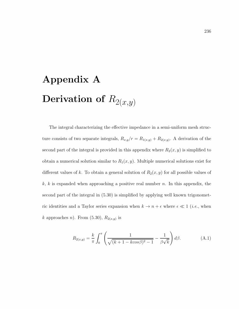
236
Appendix A
Derivation of R2(x,y)
The integral characterizing the effective impedance in a semi-uniform mesh struc-
ture consists of two separate integrals, Rx,y/r = R1(x,y) +R2(x,y). A derivation of the
second part of the integral is provided in this appendix where R2(x, y) is simplified to
obtain a numerical solution similar to R1(x, y). Multiple numerical solutions exist for
different values of k. To obtain a general solution of R2(x, y) for all possible values of
k, k is expanded when approaching a positive real number n. In this appendix, the
second part of the integral in (5.30) is simplified by applying well known trigonomet-
ric identities and a Taylor series expansion when k → n + ǫ where ǫ ≪ 1 (i.e., when
k approaches n). From (5.30), R2(x,y) is
R2(x,y) =k
π
∫ π
0
(
1√
(k + 1− kcosβ)2 − 1− 1
β√k
)
dβ. (A.1)
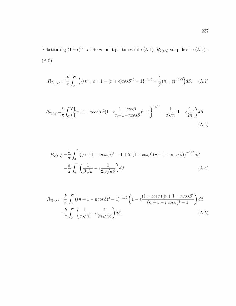
237
Substituting (1 + ǫ)m ≈ 1 +mǫ multiple times into (A.1), R2(x,y) simplifies to (A.2) -
(A.5).
R2(x,y) =k
π
∫ π
0
(
(n+ ǫ+ 1− (n + ǫ)cosβ)2 − 1−1/2 − 1
β(n + ǫ)−1/2
)
dβ. (A.2)
R2(x,y)=k
π
∫ π
0
(
(n+1−ncosβ)2(1+ǫ1− cosβ
n+1−ncosβ)2−1
−1/2
− 1
β√n(1− ǫ
1
2n)
)
dβ.
(A.3)
R2(x,y) =k
π
∫ π
0
(
(n+ 1− ncosβ)2 − 1 + 2ǫ(1− cosβ)(n+ 1− ncosβ))−1/2
dβ
−k
π
∫ π
0
(
1
β√n− ǫ
1
2n√nβ
)
dβ. (A.4)
R2(x,y) =k
π
∫ π
0
((n+ 1− ncosβ)2 − 1)−1/2
(
1− ǫ(1− cosβ)(n+ 1− ncosβ)
(n+ 1− ncosβ)2 − 1
)
dβ
−k
π
∫ π
0
(
1
β√n− ǫ
1
2n√nβ
)
dβ. (A.5)
238
R2(x,y) is grouped into two parts, as follows,
R2(x,y) =k
π
∫ π
0
(
(
(n+ 1− ncosβ)2 − 1)−1/2 − 1
β√n
)
dβ
+k
π
∫ π
0
(
−ǫ(1 − cosβ)(n+ 1− ncosβ)
((n+ 1− ncosβ)2 − 1)3/2+
ǫ
2βn√n
)
dβ. (A.6)
R2(x,y) can be numerically determined by assigning n to a constant value. For in-
stance, when k → 1 (i.e., n = 1), the first and second parts of (A.6) are numerically
determined by, respectively, assigning n = 1 and substituting ǫ = k − 1. R2(x,y)
becomes
R2(x,y) =− 0.033425k − k(k − 1)
π
∫ π
0
(
(1− cosβ)(2− cosβ)
((2− cosβ)2 − 1)3/2− 1
2β
)
dβ. (A.7)
The second integral is numerically solved and the closed-form expression for R2(x,y)
when k → 1 is
R2(x,y) = −0.033425k − 0.0629k(k − 1). (A.8)
When k approaches another constant, (A.6) is similarly determined. Closed-form
approximations for R1(x,y) and R2(x,y) are listed in Table 5.1 for different values of n,
where the effective resistance Rx,y = R1(x,y) +R2(x,y).
239
Appendix B
Closed-Form Expressions forInterconnect Resistance,Capacitance, and Inductance
Closed-form expressions for the resistance, capacitance, and inductance of a line
are summarized in this appendix to provide additional background on the effect of
technology and certain design parameters on the interconnect impedance. The inter-
connect line resistance is
R =ρL
WT, (B.1)
where ρ, L, W , and T are, respectively, the resistivity, length, width, and thickness
of the interconnect. The line-to-substrate capacitance and coupling capacitance are,
respectively, [231]
Cs
εox=
W
h+ 2.2217
(
s
s+ 0.7h
)3.193
+ 1.171
(
s
s + 1.51h
)0.7642
.
(
T
T + 4.532h
)0.1204
,
(B.2)
240
and
Cc
εox=1.144
T
s
(
h
h+ 2.059s
)0.0944
+ 0.7428
(
W
W + 1.592s
)1.144
+ 1.158
(
W
W + 1.874s
)0.1612
.
(
h
h+ 0.9801s
)1.179
, (B.3)
where εox, h, and s are, respectively, the oxide permittivity, distance from the inter-
connect to the substrate, and spacing between adjacent interconnects. Closed-form
expressions for the self- and mutual inductance of a line are, respectively, [232, 233]
Ls =µ0.L
2π
[
ln(2L
W + T) +
1
2+
0.22(W + T )
L
]
, (B.4)
and
Lm =µ0.L
2π
[
ln(2L
d)− 1 +
d
L
]
, (B.5)
where µ0 and d are, respectively, the magnetic permeability of free space and the
center-to-center distance between two adjacent interconnects.


![INTEGRATED PROJECT DELIVERY AGREEMENT · 1816211.10 [PROJECT NAME] INTEGRATED PROJECT DELIVERY AGREEMENT [Profit Deferred Until Final Completion]](https://img.pdfslide.net/doc/110x75/5f7b1be6148ce06db6337b9f/integrated-project-delivery-agreement-181621110-project-name-integrated-project.jpg)