Embed Size (px)
Citation preview
NASACR-187116
High-Power Converters for Space Applications
Phase I Final Report and Phase 2 Plans
Contract NAS3-25800
Prepared forNASA Lewis Research Center
Cleveland, Ohio
Prepared byBE Corporate Research and Develop.mentSchenectady, New Yorkand
Maxwell Laboratories, Inc.San Diego, California
June 1991
9OSRD0O8
Section
TABLE OF CONTENTS
ABSTRACT ....................................................................................................................
INTRODUCTION .........................................................................................................
1.1 Program Objectives .............................................................................................
1.2 Program Phases ....................................................................................................
HIGH-VOLTAGE OPTICALLY CONTROLLED MCT SWITCH MODULE
2.1 Background ...........................................................................................................
2.2 MCT Module Structure .......................................................................................
2.2.1 Package Concept .....................................................................................
2.2.2 Advanced Package Concept ...................................................................
2.2.3 Proposed Module Concept .....................................................................2.2.4 Rectifier Module .....................................................................................
2.3 MCT Module Simulation ....................................................................................
2.3.1 HSPICE Simulation ................................................................................
2.3.2 Snubber Circuit ........................................................................................
2.3.3 System and Module Worst-Case Simulation ........................................
2.3.4 System Simulation ....................................................................................2.3.5 Module Simulation ..................................................................................
2.3.6 Losses and Temperature Rise ...............................................................
2.4 MCT Inverter Hardware .....................................................................................
TRANSFORMER-LINKED DC-TO-DC CONVERTER SYSTEM ...................
3.1 Converter System Topology ................................................................................
3.1.1 Super-Resonant Inverter ........................................................................
Theory of Operation .........................................................................
Three-Phase Circuit Option .............................................................3.1.2 Prime Power Interaction ........................................................................
3.1.3 Load Range Interaction ..........................................................................
3.1.4 Cooling Systems .......................................................................................
3.2 High-Voltage Transformer Design ....................................................................3.2.1 Interconnection of Coils .......................................................................
3.2.2 Coil Design ...............................................................................................Conductor Selection ..........................................................................
3.2.3 Core Design ..............................................................................................Ferrite .................................................................................................
Permalloy ............................................................................................
Amorphous Metal .............................................................................Finemet ...............................................................................................
3.2.4 Packaging and Cooling ............................................................................Thermal Conduction .........................................................................
Page
xiii
1-1
1-1
1-1
2-1
2-1
2-1
2-1
2-1
2-4
2-4
2-9
2-9
2-9
2-12
2-12
2-16
2-23
2-23
3-1
3-1
3-1
3-3
3-5
3-53-7
3-7
3-73-9
3-11
3-12
3-12
3-12
3-12
3-14
3-14
3-153-15
iii PRL:_CEDIr_G PAGE BLANK NOT FILMED
Section
5
6
TABLE OF CONTENTS (Cont'd)
4.3 Critical
4.3.1
4.3.2
4.3.3
4.3.4
4.3.5
4.3.6
4.3.7
4.3.8
4.3.9
System Issues ..........................................................................................
System Weight ..........................................................................................
System Performance ................................................................................
System Efficiency .....................................................................................High-Voltage Insulation .........................................................................
Cooling ......... ......... °...° ........... .... ................................................................
Input Fuse Protection .............................................................................Fault Protectior: .......................................................................................
Reliability ............................................................................................
System Hardnc ......................................................................................
4.4 Technical Approach an_! System Description ...................................................
4.4.1 Overall System _ .'nctional Description ................................................4.4.2 Inverter .....................................................................................................
4.4.3 Resonance Transformer .........................................................................
Resonance Transformer Configuration .........................................
Inductor Design .................................................................................Capacitor Design Considerations ....................................................
Capacitor Design ...............................................................................4.4.4 Rectifier and Voltage Multiplier ...........................................................
4.4.5 Regulator ..................................................................................................4.4.6 Filter Inductor and Capacitor ................................................................4.4.7 Crowbar ....................................................................................................
4.4.8 Housing, Support, and Cooling Structures ......................... :.................
4.5 System Selection, Mass Efficiency, and Layout ...............................................
4.6 Risk Areas and Risk Abatement ........................................................................
4.6.1 Resonance Transformer-Based Systems ..............................................
4.6.2 Cryocooling ..............................................................................................4.6.3 Semiconductors in Space ........................................................................
4.64 Regulator Scheme ...................................................................................
4.7 System Scalability .................................................................................................
4.8 Summary ................................................................................................................
4.9 References ........................................................................................................
CONCLUSIONS ............................................................................................................
PROPOSED FOLLOW-ON ACTIVITY ..................................................................
Page
4-1
4-1
4-2
4-2
4-2
4-2
4-2
4-3
4-3
4-3
4-4
4-4
4-44-4
4-4
4-8
4-12
4-16
4-21
4-21
4-23
4-25
4-25
4-27
4-274-29
4-29
4-29
4-29
4-29
4-30
4-30
5-1
6-1
Figure
2.2.1-1
2.2.2-1
2.2.3-1
2.2.3-2
2.2.3-3
2.2.3-4
2.3.1-1
2.3.2-1
2.3.4-1
2.3.4-2
2.3.4-3
2.3.5-1
2.3.5-2
2.3.5-3
2.3.5-4
2.4-1
3.1-1
3.1.1-1
3.1.1-2
3.1.1-3
3.2-1
3.2-2
3.2.1-1
3.2.1-2
3.2.2-1
3.2.5-1
3.2.5-2
3.2.5-3
3.3.1-1
3.3.2-1
3.4.1-1
LIST OF ILLUSTRATIONS
Page
Hermetic Thin-Pak ..................................................................................................... 2-2
MCT module ............................................................................................................... 2-2
400-A, 1000-V MCT module; vertical view ............................................................. 2-5
400-A, 1000-V MCT module; top view .................................................................... 2-5
400-A, 1000-V MCT module; partial view .............................................................. 2-6
Schematic of MCT module and method of powering driver circuit .................... 2-7
MCT models - NPN/PNP bipolar ......................................................................... 2-10
Snubber simulation ..................................................................................................... 2-11
NASA 5-kV, 1-MW H-bridge converter ................................................................. 2-13
5-kv H-bridge HSPICE circuit .................................................................................. 2-14
1-MW H-bridge converter - output simulation ..................................................... 2-17
MCT module simulation ............................................................................................ 2-18
MCT device simulation .............................................................................................. 2-19
Reverse diode simulation .......................................................................................... 2-20
Snubber circuit simulation ......................................................................................... 2-21
Proposed MCT inverter hardware ........................................................................... 2-29
Transformer-linked dc-to-dc converter system ...................................................... 3-2
Super-resonant inverter circuit ................................................................................. 3-4
Conduction sequence for one cycle in the square-wave mode ............................. 3-4
Three-phase super-resonant converter .................................................................... 3-6
Transformer core and coil layout ............................................................................. 3-8
T/R arrangement with coils not interconnected .................................................... 3-8
T/R arrangement with corresponding layers of coils connected in series .......... 3-10
T/R arrangement with opposite layers of coils connected in series .................... 3-10
Types of ritz conductor ............................................................................................... 3-13
Transformer core dimensions ................................................................................... 3-17
Section of transformer ............................................................................................... 3-17
Half-section of transformer ....................................................................................... 3-18
Full-wave bridge rectifier .......................................................................................... 3-25
Half-wave bridge (voltage doubler) rectifier .......................................................... 3-27
Resonant inductor configuration .............................................................................. 3-30
viiPRECEDING PAGE BLANK NOT FILMED

Figure
4.4.3-5
4.4.3-6
4.4.3-7
4.4.3-8
4.4.3-9
4.4.3-10
4.4.3-11
4.4.3-12
4.4.3-13
4.4.3-14
4.4.3-15
4.4.3-16
4.4.3-17
4.4.3-18
4.4.3-19
4.4.5-1
4.4.5-2
4.4.5-3
4.4.7-1
4.5-1
LIST OF ILLUSTRATIONS (Cont'd)
Page
Symmetric series-connected resonance transformer-based
system with capacitive voltage multiplier output .................................................... 4-9
Symmetric series-connected resonance transformer-based
system simulation circuit ........................................................................................... 4-9
Symmetric series-connected resonance transformer-based
system simulation circuit results ............................................................................... 4-9
Resonance transformer inductor sketch .................................................................. 4- '
Parallel winding to divide current and thermal paths ............................................ 4-13
Winding detail ............................................................................................................. 4-13
Capacitor winding assembly series parallel construction ...................................... 4-14
Temperature coefficient of capacitance vs. temperature ...................................... 4-15
Temperature coefficient of dissipation factor ......................................................... 4-15
Electrode insulator assemblies ................................................................................. 4-17
Series capacitor constructions ................................................................................... 4-17
Center-tapped capacitor ............................................................................................ 4-19
GE and Maxwell resonance capacitor specifications ............................................ 4-20
GE and Maxwell filter capacitor specifications ..................................................... 4-20
GE and Maxwell specific weights ............................................................................. 4-20
FM modulation control simulation results .............................................................. 4-22
PWM control simulation results ............................................................................... 4-22
Regulator scheme sketch ........................................................................................... 4-24
Crowbar circuit ........................................................................................................... 4-26
High-power, high-voltage dc-dc converter system
layout with housing ..................................................................................................... 4-28
ix
Table
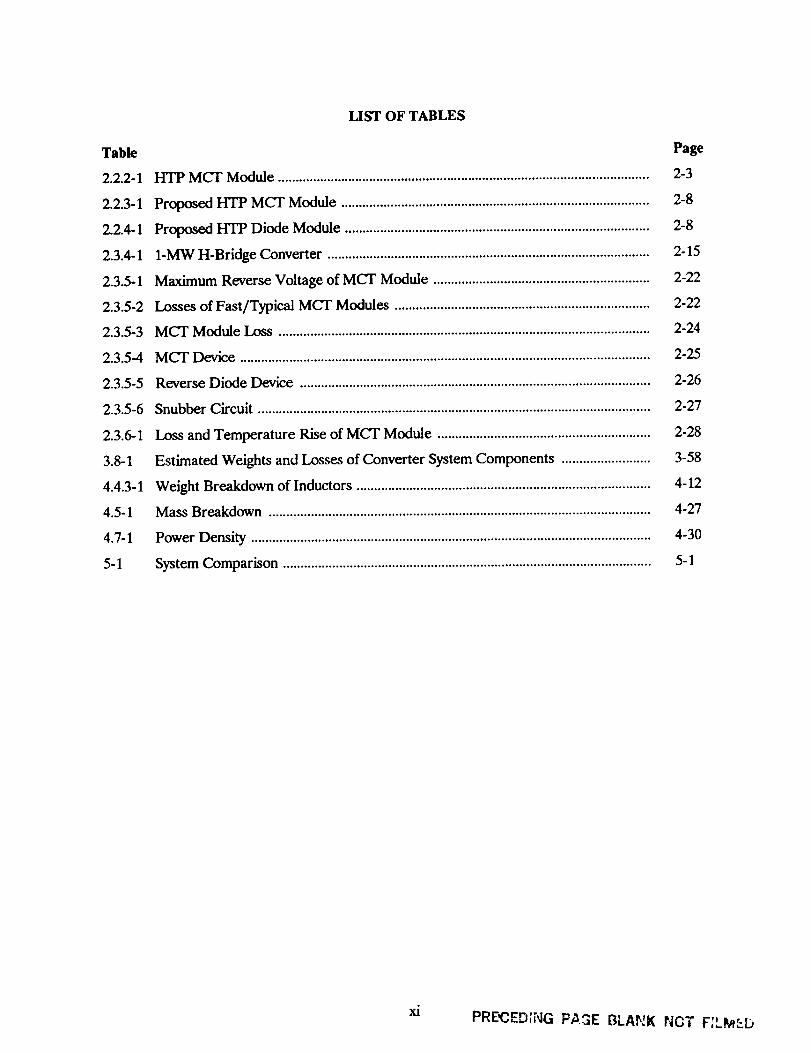
2.2.2-1
2.2.3-1
2.2.4-1
2.3.4-1
2.3.5-1
2.3.5-2
2.3.5-3
2.3.5-4
2.3.5-5
2.3.5-6
2.3.6-1
3.8-1
4.4.3-1
4.5-1
4.7-1
5-1
LIST OF TABLES
HTP MCT Module .........................................................................................................
Proposed HTP MCT Module .......................................................................................
Proposed HTP Diode Module ......................................................................................
1-MW H-Bridge Converter ...........................................................................................
Maximum Reverse Voltage of MCT Module .............................................................
Losses of Fast/Typical MCT Modules ........................................................................
MCT Module Loss .........................................................................................................
MCT Device ....................................................................................................................
Reverse Diode Device ...................................................................................................
Snubber Circuit ...............................................................................................................
Loss and Temperature Rise of Mc'r Module ............................................................
Estimated Weights and Losses of Converter System Components .........................
Weight Breakdown of Inductors ...................................................................................
Mass Breakdown ............................................................................................................
Power Density .................................................................................................................
System Comparison ........................................................................................................
Page
2-3
2-8
2-8
2-15
2-22
2-22
2-24
2-25
2-26
2-27
2-28
3-58
4-12
4-27
4-30
5-1
xJ PRE'CED_NG PA..3E BLANK NOT F;LM_-,_D
ABSTRACT
Phase 1 of this program is a concept definition effort to extend space-type de/de converter
technology to the megawatt level with an overall weight objective of less than 0.1 kg/kW
(220 lb/MW), including components, structures, and cooling capability to interface with aheat rejection system. Two advanced power conversion system designs were evaluated for
Phase 1 and both designs represent an extension of de-to-de converter technology to well
beyond the present state of the art. Either design approach operates from a 5-kV energy
source of stacked fuel cells and provides a voltage step-up to 100 kV at up to 10 A of current.
This charges energy storage capacitors for pulse discharge at rates to 100 pps at a duty cycle
of 17 min on, 73 min off. Both approaches use a full-bridge inverter having MCTs (MOS com-
mutated thyristors) as the high-power, high-speed switching device. Also, both design ap-
proaches use gaseous hydrogen cooling and a proven crowbar fault protection scheme.
The GE-CRD system utilizes an advanced design high-voltage transformer/rectifier filter
(ultra-low reflected ac capacitance) in series with a resonant tank circuit, driven by an inverter
operating at high frequency (20 to 50 kHz) to minimize the size of inductive and capacitive
components. Output voltage control is obtained through a combination of frequency and
phase shift control. Fast transient response and stability is ensured through a special protocol
called optimal control. Super-resonant operation (above the resonant frequency of the tank)employing MCTs provides the following advantages: lossless snubbing for switch protection,
no turn-on switching loss, use of medium-speed inverter diodes, no d//dt limiting required, in-
trinsic current limiting under load-fault conditions. The estimated weight of the GE-CRD sys-
tem is 88.5 kg, with an enclosed volume of 1.5 ft 3. Efficiency is estimated at 94.4% for a total
system loss of 55.711 kW when operating at 1-MW load power. The GE-CRD system is based
on technology developed for a product application and has demonstrated a high degree of reli-
ability.
The Maxwell system is based on a resonance transformer approach developed at Maxwell
Labs and avoids the use of a high-voltage transformer by combining a cascade of five LC
resonant sections operated at a fixed frequency of 100 kHz. The 5-kV bus voltage is converted
to a square wave by the inverter, stepped up to a 100-kV sine wave by the resonant action ofthe cascade of LC sections, and rectified and filtered. The inductors of the resonance
transformer do not use magnetic cores, which reduces loss and weight. The Maxwell systemhas an estimated weight of 83.8 kg and an enclosed volume of 4.0 ftL Efficiency is estimated at
87.2% for a total system loss of 146.411 kW when operating at 1-MW load power.
Plans are given for Phase 2 work for the fabrication and testing of the de/de convertersdescribed in Phase 1.
,4.
XIU
Section 1
INTRODUCTION
I.I Program Objectives
The objective of this NASA-Lewis Research Center contract with GE Corporate Re-
search and Development and Maxwell Laboratories is to extend space-type de/de converter
technology to the megawatt level, with an overall weight objective of less than 0. I kg/kW
(220 Ib/MW) including components, structures, and cooling capability to interface with a heat
rejection system. The converter will employ an inverter and a transformer (GE) or an invert-
er and a cascade of resonant L-C sections (Maxwell) to step-up the voltage from 5 kV dc to
i00 kV de. Present power converter principles must be extrapolated to simultaneously
achieve the goals of high power and high voltage, with high-frequency operation for fight
weight. Typically, the input will be stacked fuel cells at a nominal voltage of 5000 V de. It is
expected that the loads supplied by the de/de converter will need up to 100 kV of steady out-
put, or up to I0 A of current to charge energy storage capacitors for pulse discharge at ratesup to I00 pulses per second. The operational duty cycle is considered to be 17 rain (I000 s)
on and 73 rain off (90-rain orbit).
1.2 Program Phases
The program has two phases:
Phase 1 - Concept definition (present phase)
Phase 2 - A. Build and test 100-kW "proof of principle" breadboard
B. Build and test I-MW "proof of principle" breadboard
C. Build and test I-MW brassboard
Phase 1 includes preliminary design work on two alternative de-to-de converter systems
using different approaches. Based on comparative evaluation of the results, NASA may select
one or both systems for further development in Phase 2. The two systems and the responsiblecontractors are
• Transformer-linked de-to-de converter - GE-CRD
• Transformerless voltage multiplier de-to-de converter - Maxwell Labs
For each system, the following have been accomplished in Phase I:
I. Specification of components required for Phase 2.
2. Identification of research and development required for those components.3. Estimation of size, weight, and efficiency.
4. Identification of partners, subcontractors, or vendors other than GE-CRD or Maxwell
Laboratories to supply components and services in Phase 2.
I-I
Section2
HIGH-VOLTAGEOPTICALLYCONTROLLEDMCT SWITCHMODULE
2.1 Background
TheMCT representsanewclassof powerswitchingdevices.Its developmentwas made
poss_le by combining power MOS and power bipolar device concepts and process capability.Compared on a current handling basis, a 600-V MCT can conduct 1000 times and 50 times
greater current than a 600-V V-FET or a 600-V IGBT, respectively, at a very low 1.5-V for-
ward drop. The MCT's high switching speed coupled with its very low switching losses as wellas its low forward drop make this the only device available at present with which to achieve
the stringent goals for the present development.
Operation in the frequency range of 20 to 50 kHz is necessary at high efficiency to achieve
the low weight goal of this program. To generate 1 MW of power using the series super-resonant circuit topology approach operating from a 5-kV dc power source requires 10 seriesMCF modules in each of four bridge arms for a total 40 modules. Each Mc'r module devel-
oped in the present study is capable of turning off 330 A into 500 V while dissipating 760 W
for the typical case. MCT modules can be paralleled for increased current and series connect-
ed to accommodate a wide range of dc bus voltages.
2.2 MCT Module Structure
2.2.1 Package Concept
A new approach to power device packaging termed the Hermetic Thin-Pak (HTP) hasbeen developed at CRD. This package exhibits low electrical impedance, low thermal resis-
tance, and high packing density of the power chips. Modules have been designed that can ac-commodate up to nine power HTP packages.
The cross section of the HTP is illustrated in Figure 2.2.1-1 (not to scale). The silicon
chip is die bonded onto the cup-shaped copper package base. Copper foil is thermocompres-sion bonded to the aluminum contacts on the active side of the die. The lid is ceramic with
patterned copper direct bonded to the top and bottom surfaces. Copper balls provide feed-through connections between the top copper and the foil on the active side of the die. The
multiple ball contacts and lid seal are joined in a reflow solder operation. The resulting HTP
package is hermetic, has a low thermal resistance path to the cooling medium (0.3 °C/W) andhas a high standoff voltage (> 2500 V).
2.2.2 Advanced Package Concept
The HTP package process can be extended to multiple cavity packages. Figure 2.2.2-1 il-
lustrates this concept with a module containing four MCTs and two diodes as would be re-
quired for the 1-MW converter. The package is fabricated on a ceramic substrate using thedirect bond process to attach the layers of copper. The characteristics of the module are sum-
marized in Table 2.2.2-1. This concept is not proposed for the 1-MW converter because of
the present early stage of HTP development. Furthermore, this module concept does not in-dude components for the snubber and driver circuitry.
2-1
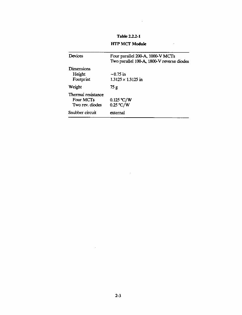
Table 2.2.2-1
HTP MCT Module
Devices
Dimensions
Height
Footprint
Weight
Thermal resistance
Four MCTs
Two rev. diodes
Snubber circuit
Four parallel 200-A, 1000-V MCTs
Two parallel 100-A, 1800-V reverse diodes
-0.75 in
1.3125 x 1.3125 in
75g
0.125 °C/W0.25oc/wexternal
2-3
CATHODE
GATE
TERMINAL BLOCK
OPTO RECEIVER ,,_ . DRIVER
CHIP
DIODE MC'r SNUBBER ANDBALANCE RESISTORS
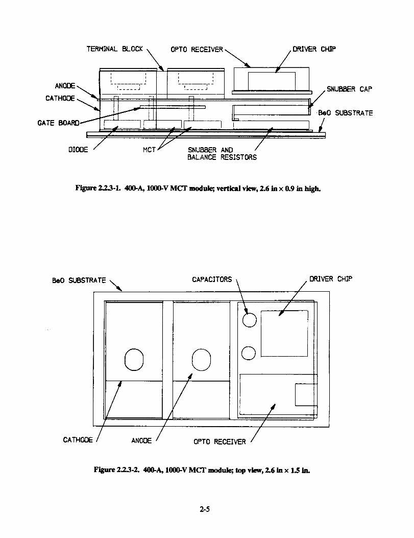
Figure 2.2.3-1. 400-A, 1000-V MCT module; vertical view, 2.6 in x 0.9 in high.
BeO SUBSTRATE,,,_
/
CAPAC]TORS DRIVER CHIP
©
c,T.o_/ ,,ooE//
©/
©
OPTO RECE]VER
/
/
Figure 2.2.3-2. 400-A, 1000-V MCT module; top view, 2.6 in x 1.5 in.
2-5
TYPIEAL MODULE
lI
I
I
I
II
I
II
III
I
J
I±
I
I
III
II
' I
II
III
I3
I
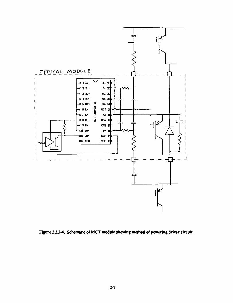
Figure 2_._4. Schemtic orMCT module showing method of powering driver circuit.
2-7

2.3 MCT MODULE SIMULATION
2.3.1 HSPICE Simulation
The MCT is a functional device comprising a four-layer PNPN bipolar structure, an ON
PMOSFET and an OFF NMOSFET. Unfortunately, no commercial simulation program for
the PNPN structure is available at the present time. Simple models have been developed in
this study with which to expedite the simulation of an MCT having PNP and N-PN back-to-back bipolar transistors, the PMOSFET, the NMOSFET and parasitic resistors.
The cross section for a stripe taken through one-half of an MCT is illustrated in Fig-
ure 2.3.1-1. A stripe taken outside of the MCT (MCTA) has bipolar transistors, the ON
PMOSFET and the OFF NMOSFET. Four inside stripes (MCTBs) have the bipolars and an
OFF NMOSFET. Initially, a model having five MCTs in parallel was developed for MCT de-vice simulation. This device model proved to be powerful in providing insight into MCT
operation, such as lateral plasma spreading and current sharing between the MCTA and
MC-'TB structures. Next, a "combined" model was developed for fast circuit simulation.
Parastic resistor values for these models were extracted from MCT dimensions and doping
profiles. Computation time for the circuit model proved to be much faster than that for the
device model. Accuracy of the two models was verified by simulations of adc chopper circuit.
The results obtained for each model are very well matched, with the exception of a negligible
discrepancy in the very rapid turn-on transient.
For the circuit simulation work, the spread of device parameters typical to production
MCI's was accounted for by developing three categories of device types: fast, typical, and
slow. The models shown in Figure 2.3.1-1 deserve the three catagories in terms of turn-off
speed and forward current capability. These models have been used to simulate both typical
and worst cases for the MCT in its present application.
The computer platform used for all of the simulation work was the VAX- 11/780 located at
CRD. The software used was HSPICE. An HSPICE-program has been tried and successfullyrun with a SUN workstation and SABRE software.
2.3.2 Snubber Circuit
A snubber (or balance) circuit equalizes the MCT turn-offvoltage sharing required for
series operation. Various types of snubbers have been applied to commercial converters.
Those circuits provide both transient and steady-state (dc) voltage balancing. Dc voltage bal-ance is accomplished with a resistive divider connected in parallel with each module of a
series string of modules. In the present case, a 100-kfl resistor across each MCT provides ade-
quate balance in compensating for inherent MCT de leakage current. Transient balancing has
been achieved by connecting a series-connected resistor and capacitor in parallel with each
MC'I" module in a series string of modules.
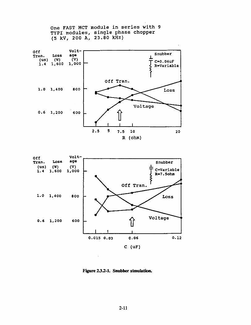
Figure 2.3.2-1 summarizes the snubber simulation results in the worst case for a single
"fast" MCT module, series connected to nine "typical" modules, operating in a single-phasedc chopper circuit. Three factors, turn-off time, total loss of the fast module and its snubber,
and the reverse voltage, have been evaluated for different snubber resistor and capacitor
values. Reviewing the results, the combination of a 7.5-n resistor and a 0.06-#F capacitor pro-
vides the best performance compromise among the variables of power loss, voltage overshoot,
and turn-off fall-time. The optimized snubber was used in the H-bridge converter simulationwork conducted in HSPICE.
2-9
One FAST MCT module in series with 9
TYPI modules, single phase chopper
(5 kV, 200 A, 23.80 kHz)
Off Volt-
Tran. Loss age J. Snubber
(us) (w) (v) T c=0.06ur
1.4 1,600 1,000 -- _ R=Variable
IOff Tran.
1.o 1,4oo 800 _.....e...._ _ L._..__os s
0.6 1,200 600 li l=
2.5 5 7.5 10 20
R (ohm)
off volt- __ __
Tran. Loss age Snubber I
(us) (w) (v) _ IT C--Variable I1.4 1,600 1,000
t R=7.5olua I
1.0 1,400 800
0.6 1,200 600 _ Voltage _
I ! t I0.015 0.03 0.06 0.12
c (uz)
Figure 2.3.2-1. Snubber simulation.
2-11
VDC
(5m_)
MCT drivers
f I0 series MCT modules
MCT module (330A, 500V)
I I I IMCT DREV MCT UI I I IMCT DREV MCTI / I _I I
ubstrkate Snubber
(22.2-35.7KHz) 0.4cm2 0.Scm?200A, 1000V 100A_ 1800V
t __ARM/ Resonant circuit
H-BRIDGE CONVERTER
Freq=20.55 IKHz
___/_ Loa_ Actual load
I I
2. Simulation
Figure 2.3.4-1. NASA 5-kV, I-MW H-bridge converter.
2-13
Table2.3.4-1
1-MW H-Bridge Converter
Cycle time (_) 45.0 42.0 37.0 28.0
Frequency (kHz) 22.222 23.80 27.03 35.71
Load resistor (fl) 19.926 41.377 84.645 190.50
Load output (kW) 1031.4 498.6 238.4 108.6
Total loss (kW) 42.4 31.4 27.7 31.2
Power efficiency (%) 96.1 94.1 89.6 77.7
Common parameters
Dc voltage
Filter capacitorResonant inductor
Resonant capacitor
Resonant frequency
Load de voltage
500O V
38.7/_F
300 t_H
0.200 tJF20.551 kHz
4546 V
Note: All modules consist of "typical" MCTs
2-15
F-resonant = 20.551 kHz
F-bridge = 22.222 kHzR-load = 19.926 Ohm
4.7
4.6
4,5
_D 4.4'
'_ 4.3,
4.a
4.1
4o
VOLTAGE
,. ,s L.. ,is =;, ,is ,. ,.s ,. i..
Time(as)
140
13S +
131 '
12S '
taO'
PG) 11SC ,
LU
110
lOS
11t0
IS
9090
JOULE
I! ill llS |1t Ill 111 tlS 131 13S
Time (p.s)
Figure 2.3.4-3. I-MW H-bridge converter - output simulation.
2-17
Nu
_40
I !
o-,-_
g_I1o
o
J _ .
(A) eOe;pA
o
. '_ ; , , . .
(v) _.e_no
2-19
o t Iu_Xu_
O,...4OX_X
0
_ 0
000
E_ E_ E_
H U H
E_H_
N
_°@
olo .0
N g
0
g_O0
0
, i
(M_) Je,v,ocl
0
III
I
.v
Ol
E I | - ! - , .* -(A) eOmlOA
:_EI-
|
o •': E
I-
f_
r_0
0A
I
0
Z
0
oA!
0
(r_u)_SJeu_
L_M •
f_
Z0
(v) _uauno
i
m E-, _,,
_ I
.., .-
• E
Q_• E:p
|
2-21
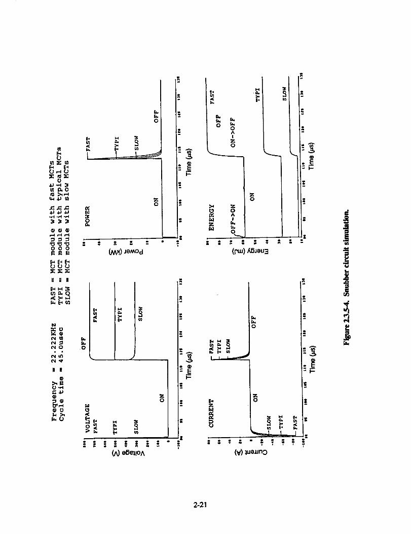
Table 2.3.5-3 tabulates loss for the MCT modules at different frequencies. The MCT de-vice loss decreases at higher frequencies because output power and therefore device peak cur-
rent is decreasing. Snubber loss increases with frequency and is therefore a maximum at
35.71 kHz. The net result of these competing loss mechanisms is a decrease in total loss to
27.03 kHz followed by an increase at 37.71 kHz.
The worst-case loss for the MCT module is 1440 W for a fast module, occurring at
22.22 kHz. For the system worst case, the data for the typical case applies. As an example, the1060 W for a typical module loss multiplied by 40 modules yields 42.22 kW at 22.22 kHz,
which yields 42.22 kW of loss for the system worst case.
Power loss for each type of MCT device is summarized in Tables 2.3.5-4 through 2.3.5-6.
MCT device power loss decreases with increasing frequency from 22.22 to 35.71 kHz (Table2.3.5-4) with the greatest power loss being exlu'bited by all three MCT types at 22.22 kHz.
The reverse diodes show less dependency on module types because they are active onlyduring the ON transient. As shown in Table 2.3.5-5, forward current decreases very rapidly at
higher frequency. Loss is always negligibly small.
The snubber circuit losses in Table 2.3.5-6 can be summarized as follows: Loss in the R-C
snubber is a function of reverse voltage and frequency. Snubber loss for the typical module isproportional to frequency, because the reverse voltage is constant at 500 V. Snubber loss for
the fast module is roughly constant, because the reverse voltage decreases at higher frequen-cy. Snubber loss for the slow module increases very rapidly with increasing frequency becausethe reverse voltage increases with frequency. Snubber loss in the worst case occurs with thefast module at 35.71 kHz.
2.3.6 Losses and Temperature Rise
Table 2.3.6-1 tabulates the losses for the MCT module, MCI" device, reverse diode, and
snubber for the typical and worst case. The heat generated by these losses is to be removed bythe cooling system. The substrate temperature is assumed to be 0 °(2. The thermal resistances
for the MCT and reverse diode are 0.125 and 0.25 °C/W, respectively. Temperature rise fromthe heat sink to the MCT junction is 100 °(2 in the worst case.
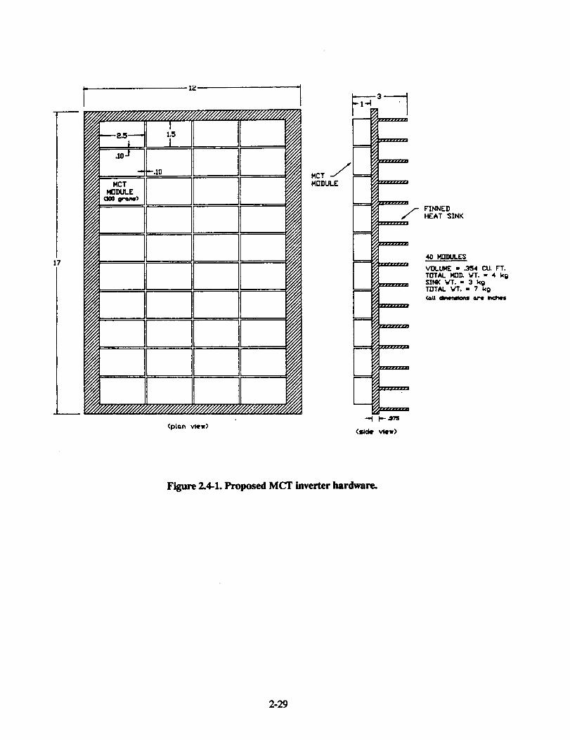
2.4 MCT Inverter Hardware
A sketch of the proposed MCT inverter hardware is shown in Figure 2.4-1. The inverterhardware structure comprises 40 MCT modules mounted on a heat sink and interconnected
electrically by a power bus structure (not shown). The 12x 17-in mounting surface area is dic-
tated by the 1.5 x 2.5-in module footprint, assuming 0.1 in intermodule spacing and some edge
margin. The heat sink is shown as a finned structure to support convection hydrogen cooling.The total volume is 0.354 fta and the mass is estimated at 7 kg exclusive of the power bus elec-
trical system. The mass of the bus system is estimated to be 1 kg, which yields a total mass of8 kg for the inverter hardware.
2-23
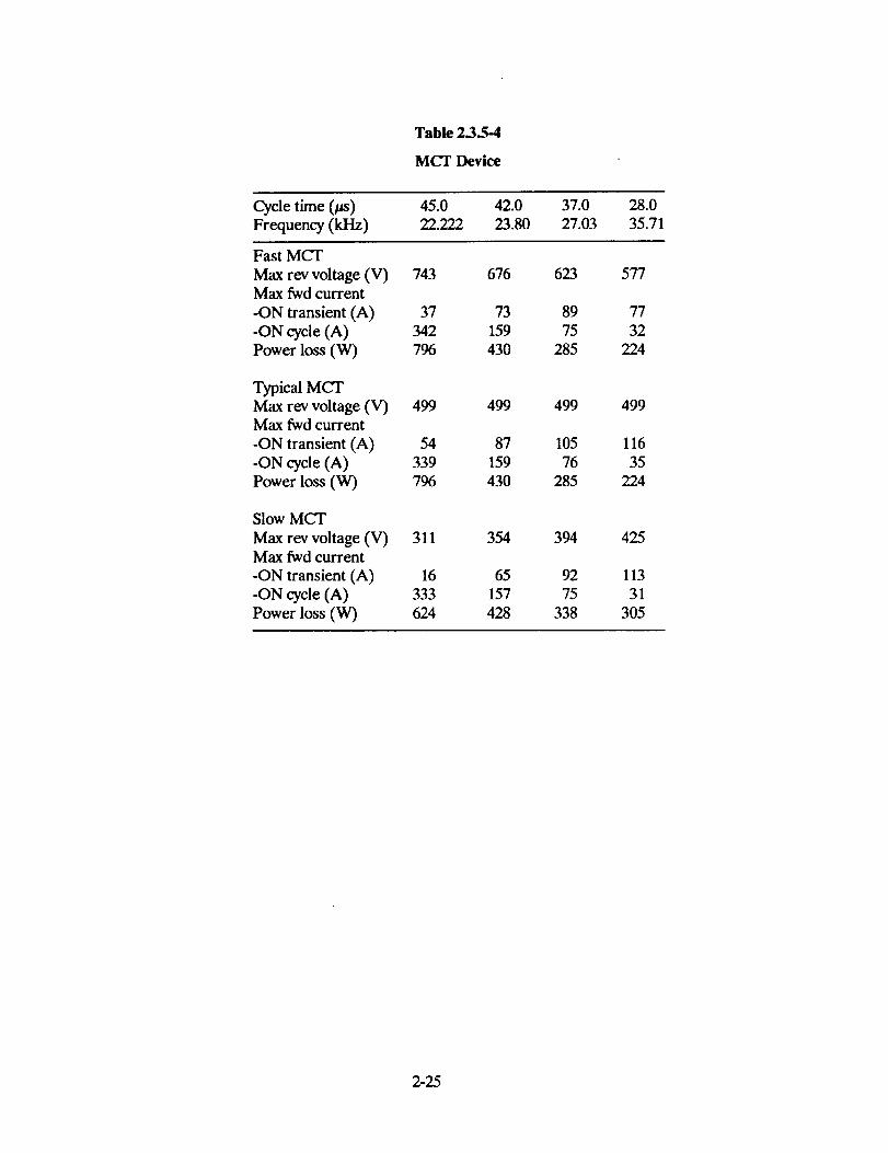
Table 2.3.5-4
MCT Device
Cycle time (_s) 45.0 42.0 37.0 28.0
Frequency (kHz) 22.222 23.80 27.03 35.71
Fast MCT
Max rev voltage (V) 743 676 623 577Max fwd current
-ON transient (A) 37 73 89 77
-ON cycle (A) 342 159 75 32
Power loss (W) 796 430 285 224
Typical MCI"Max rev voltage (V) 499 499 499 499Max fwd current
-ON transient (A) 54 87 105 116
-ON cycle (A) 339 159 76 35
Power loss (W) 796 430 285 224
Slow MCT
Max rev voltage (V) 311 354 394 425Max fwd current
-ON transient (A) 16 65 92 113
-ON cycle (A) 333 157 75 31
Power loss (W) 624 428 338 305
2-25

Table 2.3.5-6
Snubber Circuit
Cycle time (_) 45.0 42.0 37.0 28.0
Frequency (kHz) 22.222 23.80 27.03 35.71
BAL of fast module
Max rev voltage (V) 743 676 623 577Peak current
-Negative (A) -86 -83 -76 -70
-Positive (A) 72 72 68 60
Power loss (W) 639 580 566 651
BAL of typical module
Max rev voltage (V) 499 499 499 499Peak current
-Negative (A) -57 -58 -59 -59
-Positive (A) 56 58 59 60
Power loss (W) 279 329 378 507
BAL of slow module
Max rev voltage (V) 311 354 394 425Peak current
-Negative (A) -34 -40 -46 -49
-Positive (A) 44 49 53 54
Power loss (W) 136 184 254 386
2-27
12
I_2o5_ 1.5
.lOJ
-" _.10
NCTMnDULE
v,m,M)
MCT J
MDDULE
FINNEDHEAT SINK
174O MOOULE$
VOLUME 1 .354 CU. F'T.TDTAL MD_ _/T. 1 4 kgSINK VT. 1 3 kgTDTAL VT. = 7 kQ
{oil c_q_nmons ,rare Iw:h_l
z_//////////////////////////////////////////////_'///////,_.
(pLcm view)
Figure 2.4-1. Proposed MCT inverter hardware.
2-29
Section3
TRANSFORMER-LINKED DC-TO-DC CONVERTER SYSTEM
3.1 Converter System Topology
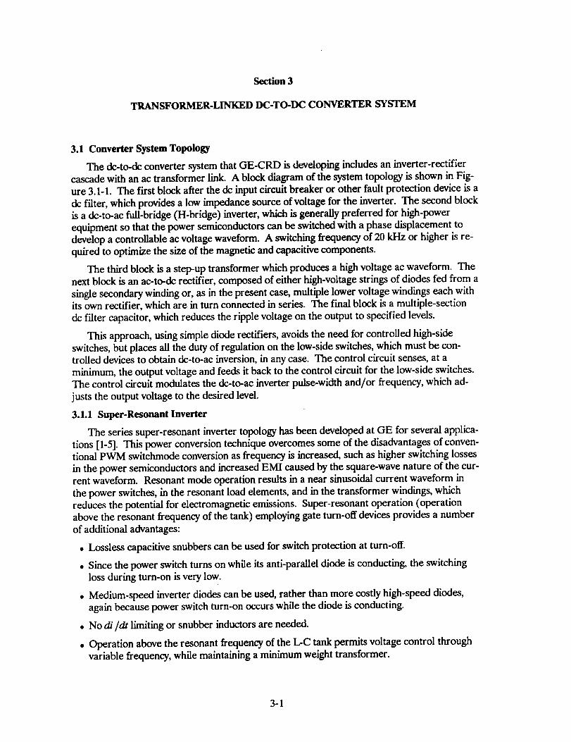
The de-to-de converter system that GE-CRD is developing includes an inverter-rectifiercascade with an ac transformer link. A block diagram of the system topology is shown in Fig-
ure 3.1-1. The first block after the de input circuit breaker or other fault protection device is a
dc filter, which provides a low impedance source of voltage for the inverter. The second block
is a de-to-at full-bridge (H-bridge) inverter, which is generally preferred for high-power
equipment so that the power semiconductors can be switched with a phase displacement todevelop a controllable ac voltage waveform. A switching frequency of 20 kHz or higher is re-
quired to optimize the size of the magnetic and capacitive components.
The third block is a step-up transformer which produces a high voltage ac waveform. Thenext block is an ac-to-de rectifier, composed of either high-voltage strings of diodes fed from a
single secondary winding or, as in the present case, multiple lower voltage windings each withits own rectifier, which are in turn connected in series. The final block is a multiple-section
dc filter capacitor, which reduces the ripple voltage on the output to specified levels.
This approach, using simple diode rectifiers, avoids the need for controlled high-side
switches, but places all the duty of regulation on the low-side switches, which must be con-trolled devices to obtain de-to-at inversion, in any case. The control circuit senses, at a
minimum, the output voltage and feeds it back to the control circuit for the low-side switches.The control circuit modulates the de-to-at inverter pulse-width and/or frequency, which ad-
justs the output voltage to the desired level.
3.1.1 Super-Resonant Inverter
The series super-resonant inverter topology has been developed at GE for several applica-
tions [1-5]. This power conversion technique overcomes some of the disadvantages of conven-tional PWM switchmode conversion as frequency is increased, such as higher switching losses
in the power semiconductors and increased EMI caused by the square-wave nature of the cur-rent waveform. Resonant mode operation results in a near sinusoidal current waveform in
the power switches, in the resonant load elements, and in the transformer windings, whichreduces the potential for electromagnetic emissions. Super-resonant operation (operation
above the resonant frequency of the tank) employing gate turn-off devices provides a number
of additional advantages:
• Lossless capacitive snubbers can be used for switch protection at turn-off.
• Since the power switch turns on while its anti-parallel diode is conducting, the switching
loss during turn-on is very low.
• Medium-speed inverter diodes can be used, rather than more costly high-speed diodes,
again because power switch turn-on occurs while the diode is conducting.
• No d//dt limiting or snubber inductors are needed.
• Operation above the resonant frequency of the L-C tank permits voltage control through
variable frequency, while maintaining a minimum weight transformer.
3-1
• The parasitic leakage inductance of a high-voltage transformer can be utilized as part ofthe resonant load.
• The current-source nature of the resonant inverter provides a safety margin under load
fault conditions and permits the paralleling of power stages for increased rating.
Control of the output voltage is achieved through a combination of frequency modulation
[6] and phase modulation. The operating frequency will be in the range 20 to 50 kHz.
Transformer winding capacitance, magnetizing inductance, and leakage inductance aresecond-order effects that modify the ideal series-resonant behavior of the converter circuit. In
particular, the effect of winding capacitance is quite critical, and a transformer design to mini-
mize the effective ac capacitance is necessary.
rneoo, of
The inverter power stage (Figure 3.1.1-1) is a full-wave bridge using MCTs with anti-
parallel fast diodes for the power switch. Snubber capacitors are placed across each power
switch. Operating in a nearly lossless manner under FM control, the snubbers are used
chiefly to limit dv/dt for EMI suppression and to assist the anti-parallel diodes in limiting
voltage overshoot at the close of a conduction cycle caused by diode turn-on time. The dc bus
capacitor bank must carry the ac component of the input current while maintaining very low
ripple at the operating frequency. The gate drivers provide positive voltage for MCT turn-onand conduction and a negative voltage for turn-off and maintenance of the off state. The in-
verter output voltage (VAn) is applied directly to the primary winding of the high-voltagetransformer in series with the resonant tank.
For simplifying the following discussion of inverter conduction modes, (Figure 3.1.1-2), the
high-voltage transformer, its output rectifier, the filter capacitors, and the load have been re-placed by a voltage source (the charged output capacitor) inserted in a full-wave bridge
rectifier. The conduction sequence during one cycle of operation in FM control mode for
super-resonant operation (where the series resonant load behaves inductively) is shown in
Figure 3.1.1-2, where the heavy lines indicate those components that are conducting current.Simultaneous conduction of Q1 and 04 has resulted in the resonant increase in current in the
arrow direction of Figure 3.1.1-2a. Simultaneous turn-off of Q1 and Q2 results in the rapid
fall of the node A voltage (rise of node B voltage), because the load current is transitioned to
the node capacitance (snubber capacitance plus device and stray capacitances). The tank cur-
rent remains essentially constant during the relatively short transition time due to the action ofthe resonant inductor. Node B voltage falls (node A voltage rises) until the anti-parallel
diodes D2 and D3 conduct, clamping the node voltages to a diode drop relative to the rail
voltages.
In the conduction mode (diode conduction) that results (Figure 3.1.1-2b), the current de-
creases to zero. Early in the diode conduction interval, Q2 and Q3 are switched on, after a
short "lockout" interval to prevent potentially disastrous "shoot-through" or simultaneousconduction of Q1 and Q2 or Q3 and 04. The current now reverses, increasing in magnitude
resonantly via the switches Q2 and Q3 (Figure 3.1.1-2c). Simultaneous turn-off of the powerswitches Q3 and Q2 is commanded by the control circuit (at a time in the conduction cycle,
which is determined by the required average current), resulting in the rapid fall of the node B
voltage (rise of node A voltage) caused by the transition of load current to the node capaci-
tance, as discussed earlier. Pickup of the current by the anti-parallel diodes D1 and 194 results
in the conduction mode of Figure 3.1.1-2d. After the lockout interval, switches Q1 and Q2 are
turned on and the conduction mode of Figure 3.1.1-2a results, completing the inverter conduc-
tion cycle.
3-3
The full H-bridge configuration is more suitable for high-power equipment and also al-
lows operation with a phase shift between switching of the two legs. This applies a quasi-square wave of voltage to the resonant circuit, and affords another method of voltage control,
in addition to frequency adjustment. The flexa"oility of the circuit is much improved, and it
may be operated over a wider range of load at nearly constant frequency, which is desirable in
most applications.
In summary, a super-resonant converter needs only shunt capacitor snubbers, which are
quite small with high-speed turn-off devices and, in any case, operate in a lossless mode. Thedevices turn on as the resonant current crosses from an anti-parallel diode at near-zero volt-
age, so turn-on loss is practically eliminated. The smoother current switching reduces EMI.
Resonant converters can be designed for serf-protection by limiting overloads, a necessary
feature in high-voltage systems where random voltage breakdown is almost unavoidable [7].
Three-Phase Cin:uit Option
At conventional power frequencies, practically all high-power equipment is configured in a
3-phase circuit arrangement. At some power level the reduced total rating of a 3-phase circuit
overcomes the disadvantage of division into three parts. At 60 Hz, a 1-MW converter would
certainly be a 3-phase circuit. A 3-phase version of the present series super-resonant convert-
er is shown in Figure 3.1.1-3. Operating at 20 kI-Iz, this arrangement will become lighter than
the single-phase circuit at some power level. This power level may be above or below 1 MW;
to our knowledge, no tradeoff study has been done. It may be worthwhile to conduct such a
study at the start of Phase 2.
In Figure 3.1.1-3, three single-phase H-bridges are operated with a mutual 120-degree
phase displacement. Each bridge generates an adjustable quasi-square wave for voltage con-
trol, which is applied to an individual series-resonant L-C tank circuit in series with a primary
winding of the main transformer. The main transformer is wound on a 3-phase E-core. Asmall auxiliary transformer (about 3% of the main transformer in size) has three coupled
windings (one in each phase) that absorb the zero-sequence voltages (third harmonic and its
multiples), eliminating these components from the rest of the circuit. This allows a significant
reduction in the rating of the main transformer and of the resonant inductors.
The high-voltage secondary windings are connected in delta to a 3-phase bridge dioderectifier and filter capacitor. As in the single-phase case, there are N sections corresponding
to the N layers of the secondary windings, which are connected in series on the dc side. The
ripple at both input and output is 6-pulse (6 * 20 kI-Iz = 120 kHz) instead of 2-pulse
(2 * 20 kHz = 40 kHz), which greatly reduces the size of the filter capacitors. While the total
rating of the components is reduced, the H-bridges, the series capacitance and inductance,and the transformer coils are divided into three parts, which may increase their physical size.
3.1.2 Prime Power Interaction
The behavior of the prime power source, assumed to be an array of fuel cells, is a critical
factor in the design of the power converter. In a specific system, the steady-state (de)
voltage-current characteristics under best- and worst-case extreme conditions are required for
establishing the range of input variables that the converter must accommodate. The series
super-resonant power converter circuit, with suitable design, will be able to operate from a
variable source having the characteristics of typical fuel cells. However, for the present pre-
liminary study, NASA has requested that an ideal source at fixed voltage be assumed, so that
size and weight estimates will approach the best attainable. For a number of reasons, it ap-
pears that an input voltage of 5000 V will be near optimum for achieving minimum size, so
3-5
this value will be assumed for the present study. Then, for 1 MW, the average dc current will
be 200 A, neglecting losses.
The maximum ac ripple current that the power source can tolerate, or the maximum rip-
ple voltage that the converter can tolerate, will determine the design of the input filter. Be-
cause no requirements have been specified, a typical condition has been assumed for the
present study. The rms ac ripple current from the power source to the converter at full load is
about 100 A. Assuming that a maximum rms ripple voltage of 10% (500 V) is allowable, thenthe source impedance must be limited to 5 fl at the ripple frequency of 40 kHz. The input
filter capacitance having this reactance is 0.8 #F.
3.1.3 Load Range Interaction
A second critical factor for the design of the power converter is the characteristics of the
load. In particular, the range of load current is needed for establishing the range of output
variables that the converter must accommodate. This is important for the design and stabili-
zation of the control system. Also, the maximum ac ripple voltage and current that the loadcan tolerate will determine the design of the output filter. For the present design, the output
filter capacitance Ca = 80 nF has been selected to reduce the output ripple voltage (at40 kHz) to less than 0.25% rms. This will store 400 J at 100 kV, requiring a crowbar for pro-tection of the load.
3.1.4 Cooling Systems
Efficient removal of heat from the converter system can have a significant impact upon
weight and size. With the option of cryogenic cooling using liquid hydrogen, it is feas_le to
maintain a cold plate at any desired temperature above 21 K. The cooling system design then
reduces to selecting an optimum operating temperature and achieving a reasonable thermal
gradient from the hot spots to the cold plate. Alternatively, as in our present concept for cool-
ing at least the transformer, a similar system employing hydrogen gas circulation to maintain
an optimum operating temperature can be used.
NASA has indicated that a reasonable assumption for the duty cycle of typical loads that
can be fed by the converter is 1000 s operation at full load in an orbital period of 90 min, or
18.5%. This will be helpful in the thermal design of the transformer, but the semiconductorswitches will have a much shorter time thermal constant, and will be subject to effectively con-
tinuous duty.
3.2 High-Voltage Transformer Design
Of the total weight objective of 100 kg for a 1-MW converter, about 35 kg can be allocated
to the transformer. The design frequency for the transformer will be the minimum operating
frequency of 20 kHz, since at higher frequencies the flux level will be reduced, such that the
core loss will be lower. For operating bursts of 1000 s with intervals for cooling, the relatively
long thermal time constant of the magnetic structure will allow higher losses than for a con-
verter in continuous operation.
A special high-voltage transformer-rectifier design is needed to minimize reflected capaci-
tance at the primary side of the transformer. In the proposed core-type structure (Fig-
ure 3.2-1), two coils are employed, one on each leg of the core. The primary windings areconnected in parallel. This arrangement has lower weight than a shell-type structure, with a
single coil on one leg of the core, or on the center leg of an E-core. The secondary windings
are dMded into sections, each feeding a section of the rectifier. By making series connections
of these sections on the de side (Figure 3.2-2), the effective ac capacitance reflected to the pri-
3-7
marysidecanbereducedto thelowvaluerequiredfor properoperation and simple control of
the series super-resonant inverter. In Figure 3.2-2, each section of the secondary winding is a
single layer, and all the de capacitors are equal in value.
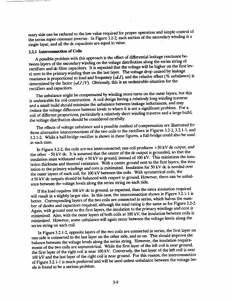
3.2.1 Interconnection of Coils
A poss_le problem with this approach is the effect of differential leakage reactance be-tween layers of the secondary winding on the voltage distr_ution along the series string of
rectifiers and de filter capacitors. It is expected that the voltage will be higher on the first lev-
el next to the primary winding than on the last layer. The voltage drop caused by leakage
reactance is proportional to load and frequency (agd), and the relative effect (% unbalance) is
determined by the factor (ad_,I/l O. Obviously, this is an undesirable situation for the
rectifiers and capacitors.
The unbalance might be compensated by winding more turns on the outer layers, but this
is undesirable for coil construction. A coil design having a relatively long winding traverse
and a small build should minimize the unbalance between leakage inductances, and mayreduce the voltage difference between levels to where it is not a significant problem. For a
coil of different proportions, particularly a relatively short winding traverse and a large build,
the voltage distr_ution should be considered carefully.
The effects of voltage unbalance and a possible method of compensation are illustrated for
three alternative interconnections of the two coils to the rectifiers in Figures 3.2-2, 3.2.1-1, and
3.2.1-2. While a half-bridge rectifier is shown in these figures, a full-bridge could also be usedin each case.
In Figure 3.2-2, the coils are not interconnected; one coil produces + 50 kV de output, and
the other - 50 kV de. It is assumed that the center of the de output is grounded, so that theinsulation must withstand only __.50 kV to ground, instead of 100 kV. This minimizes the insu-
lation thickness and thermal resistance. With a center ground next to the first layers, the insu-
lation to the primary windings and core is minimized. Insulation for 50 kV de is needed over
the outer layers of each coil, for 100 kV between the coils. With symmetrical coils, the
+_50 kV de outputs should be balanced with respect to ground. However, there can be unbal-
ance between the voltage levels along the series string on each side.
If the load requires 100 kV de to ground, as expected, then the extra insulation requiredwill result in a slightly larger size. In this case, the interconnection shown in Figure 3.2.1- I is
better. Corresponding layers of the two coils are connected in series, which halves the num-
ber of diodes and capacitors required, although the total rating is the same as for Figure 3.2-2.
Again, with ground next to the first layers, the insulation to the primary windings and core isminimized. Also, with the outer layers of both coils at 100 kV, the insulation between coils is
minimized. However, some unbalance will again occur between the voltage levels along theseries string on each coil.
In Figure 3.2.1-2, opposite layers of the two coils are connected in series; the first layer on
one side is connected to the last layer on the other side, and so on. This should improve the
balance between the voltage levels along the series string. However, the insulation require-ments of the two coils are asymmetrical. While the first layer of the left coil is near ground,
the first layer of the right coil is near 100 kV. Conversely, the last layer of the left coil is near
I00 kV and the last layer of the right coil is near ground. For this reason, the interconnection
of Figure 3.2.1-1 is much preferred and will be used unless unbalance between the voltage lev-
els is found to be a serious problem.
3-9

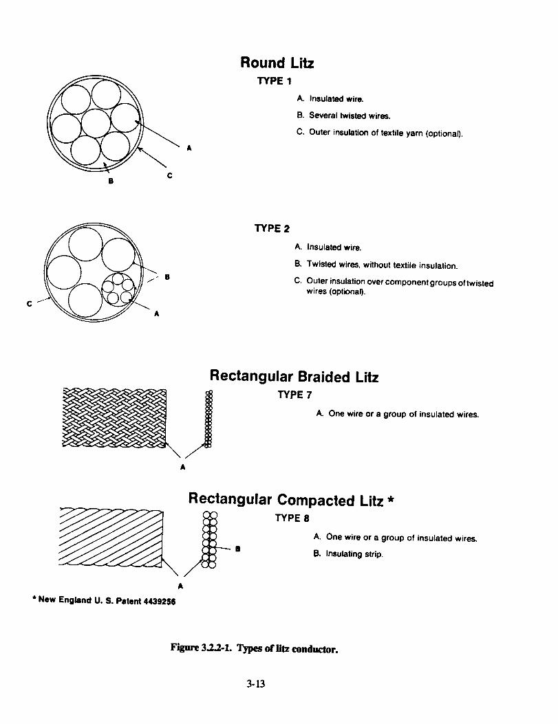
3.2.2Coil Design
The coil design for a high-frequency, hi_-voltage, high-power transformer is particularly
difficult if light weight is desired. Conventional commercial designs of high-voltage coils rely
on paper and oil or air as the major insulation to ground. Using a conservative value of the
voltage gradient allowed across such insulation, which occupies much more window spacethan the copper because of wide spacing from coil to ground, it is found that a large, heavy
core is required. The overall size of the transformer is greatly affected by the voltage rating,
and the variation with current (power) rating is relatively small.
It was concluded from earlier studies that any transformer design using oil (or other fluid)
alone as the major insulation to ground cannot meet the size goals. Tight enclosure of at least
the secondary windings in some material allowing significantly higher voltage gradient stressesseems to be the solution. The use of interlayer insulation that permits higher voltage gra-
dients is also indicated. However, such high-gradient insulating materials have higher dielec-
tric permittMty than oil, gas or paper. Because the spacing is closer and the dielectric permit-
tivity is higher, an increase in capacitance results from both factors. The resolution of this
difficulty is to divide the secondary windings into sections, each feeding a section of the
rectifier, as previously discussed.
To implement this construction technique, the design and manufacture of the high-
gradient coil forms is critical. Integration of each layer of the secondary winding with a sec-tion of the rectifier and filter capacitor is necessary to minimize the insulation space and the
ac winding capacitance. The high-voltage secondary windings will be completely enclosed
within precision-molded solid insulation forms of a material such as polypropylene, for which
a design gradient of 800 kV/cm (2 kV/mil) is assumed. Sections of the coil forms must fit to-
gether very tightly (0.1 mm press fit), so that the high-gradient electric field is contained
within the assembly and the high dielectric strength of polypropylene allows close spacing to
the core and nearby grounded structures.
In making forms of this type, proper allowances must be made for shrinkage and otherfactors; size and shape limitations could restrict the options of transformer geometry. A filler
material such as talcum powder may be used to increase the thermal conductivity. The cost of
making the molds for the forms is expected to be high, so the design should be firm before
manufacture. Therefore, it is proposed that the coil forms be fabricated by other methods
during this development program, postponing the use of molds until any future production isundertaken.
Our original concept was to enclose the rectifier diodes and de filter capacitors with the
secondary windings in extended forms of polypropylene insulation, distributing the diodes and
capacitors around the periphery of the coil. In this way, all the high-voltage interconnections
except the output lead are contained within the high-gradient insulation system. This type of
construction has been used in a commercial application at a lower power level and low dutycycle, where thermal problems are not acute. However, because of the disparity in the heat
generation and temperature limits of the transformer coils, the rectifier diodes, and the capac-itors, this concept has been modified. We now propose to group the diodes and capacitors at
one end of the transformer, perhaps with a polypropylene conduit for the many leads. This
arrangement allows the outer surface of the coils to be in direct contact with the cooling medi-um.
3-11
A
CB
Round LitzTYPE 1
A. Insulated wire.
B. Several twisted wires.
C. Outer insulation of textile yarn (optional).
CA
TYPE 2
A. insulated wire.
B. Twisted wires, without textile insulation.
C. Outer insulation over component grOUlDSof twisted
wires (optional).
Rectangular Braided LitzTYPE 7
A. One wire or a group of insulated wires.
A
Rectangular Compacted Litz *
A
B
TYPE 8
A. One wire or a group of insulated wires.
B. Insulating strip.
* New England U. S. Patent 4439256
Figure 3.2.2-1. Types of iitz conductor.
3-13
3.2A Packaging and Cooling
The thermal and packaging design of the high-voltage transformer-rectifier is a critical
problem in minimizing weight. In our original concept, the rectifier diodes and tic filter ca-
pacitors were to be enclosed with the secondary windings in extended forms of polypropylene
insulation, distr_uting the diodes and capacitors around the periphery of the coil. This as-
sembly was to be enclosed together with the resonant inductor in an aluminum tank filled withoil for insulation and cooling. The dielectric liquid (isopropylbiphenyl) proposed by Maxwell
Laboratories for impregnating the capacitors can also be used for the transformer and induc-
tor. A very much simplified initial analysis of the thermal behavior of the system indicated
that cooling will be difficult. The thermal dissipation at the surfaces of the core and coils is
high, and forced fluid cooling in addition to conduction is necessary.
In the presence of high-frequency magnetic fields, metal tubing for the cooling fluid is un-
desirable, as are metal sinks for conducting heat. Therefore, forced convection of the liquid
insulating oil, in direct contact with the transformer structure, was proposed. The oil would
be cooled in a liquid hydrogen heat exchanger. With the high-voltage windings surrounded by
the rectifier and filter capacitors enclosed in solid insulation, rendering the oll inside stagnant,
conduction of heat through this structure to the outer surface was a severe limiting factor.
The poor thermal conductMty of the insulating material and the desired temperature limit of60 °(2 for the polypropylene filter capacitors are particularly limiting, especially in view of theadded losses of the rectifier diodes.
Because of the disparity in the heat generation and temperature limits of the transformer
coils, the rectifier diodes, and the filter capacitors, our original concept for enclosing thesecomponents with the secondary windings in solid polypropylene insulation was modified. We
now propose to group the diodes and capacitors at one end of the transformer, perhaps with
an insulating conduit for the many leads. This arrangement allows the outer surface of the
coils to be in direct contact with the cooling medium. All these components and the resonant
inductor are still expected to be contained within the transformer tank. Detailed work on heat
transfer in this arrangement has confit_med that forced oil cooling will be effective. Because
many of the heat transfer formulas are quite complex, computer routines were written to
speed the calculations and to allow tradeoff options to be studied in depth.
However, to eliminate the weight of an oil to liquid hydrogen heat exchanger, the idea of
employing direct gaseous hydrogen cooling is now proposed, as in the scheme conceived by
Maxwell Laboratories for their converter system. This should also allow the metal tank to be
replaced by a lightweight enclosure, including the inverter and all other components as well.
Estimates of heat transfer coefficients obtainable with gaseous hydrogen cooling show that itis feas_le and should save considerable weight, but the effect on the dielectric insulation sys-
tem will need further study in Phase 2. The heat transfer coefficient is less than for compara-
ble oil cooling, leading to a higher but not critical temperature rise.
T/m, ma/_
Small size leads to high losses per unit volume, resulting in large thermal gradients and a
significant rise within the core and coils of the hot-spot temperature above the surface tem-
perature. Literature on the difficult problem of calculating the hot-spot temperature was con-sulted. A relatively simple method of analyzing the thermal behavior of the system was devel-
oped, leading to a formula for estimating the temperature rise of cores and coils with aniso-
tropic thermal properties. This should be sufficiently accurate for engineering design pur-poses, at least in the present Phase 1 of this project. In later phases, it may be desirable to
3-15
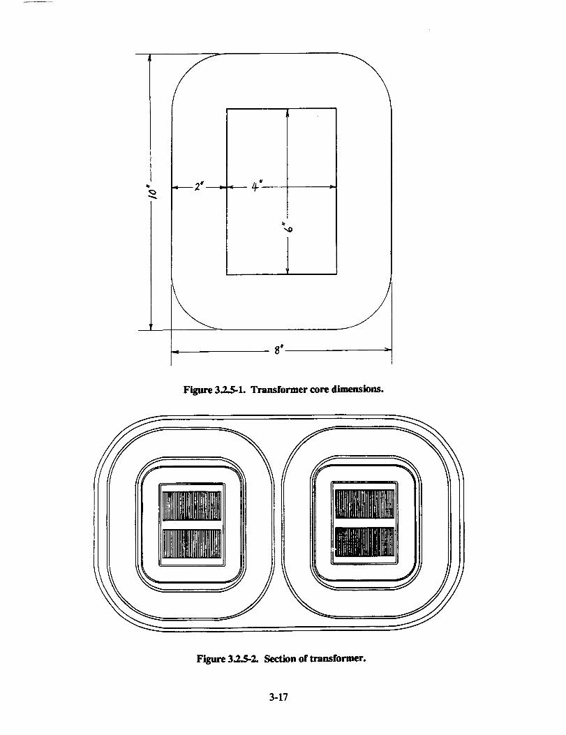
&
1
Figure 32.5-1. Transformer core dimensions.
/
I
II
i
iiI
Figure 32.5-2. Section of transformer.
3-17

Bas/e Parameters
Design frequency
Coolant inlet temperature
Primary voltage (square wave)
Secondary voltage (square wave)
Primary current (sine wave)
Secondary current (sine wave)Estimated per unit regulation
Primary coil voltage to ground
Secondary coil voltage, first layer to ground
Secondary coil voltage, last layer to ground
Design flux density (average over section)
20,000 Hz
300 K (27 *¢)5,000 V
100,000 V
126.5 Arms
23 Arms
0.1
5,000 V
10,000 V
100,000 V0.8 T
Copper Conduem_
Design current density
Electrical resistivityTemperature coefficient of resistance
Specific gravity
Thermal conductivity
Specific heat
2400 A/in 21.724E-6 ohm-cm at 20 *C
0.00393
8.96 g/cm 3
394 W/m.K
0.091 cal/g.K (0.382 J/g.K)
Co//Insu/at/on
All solid insulation (coil form, interlayer, intercoil, cover) is assumed to be fabricated of a
material such as polypropylene, for which a design gradient of 800 kV/cm (2 kV/mil) is as-sumed.
Dielectric constant
Specific gravity
Thermal conductivity
Specific heat
Design voltage gradient
Creepage field gradient (interlayer)
2.3
0.9 g/cm 3
0.117 W/m.K
0.5 cal/g.K (2.093 J/g.K)
200oV/mil20V/ma
Core P_
Core material
Specific gravity
Thermal conductivitySpecific heat
Stacking factor
Flux density (in iron)
Flux density (average over section)Core section width
Core section build
Core window heightCore window breadth
Metglas 2605S-3A
7.29 g/crn 3
9.0 W/m.K
0.13 cal/g.K (0.544 J/g.K)0.75
1.076 T
0.807 TD= linx2 = 2in
E =2in
F=4in
G=6in
3-19
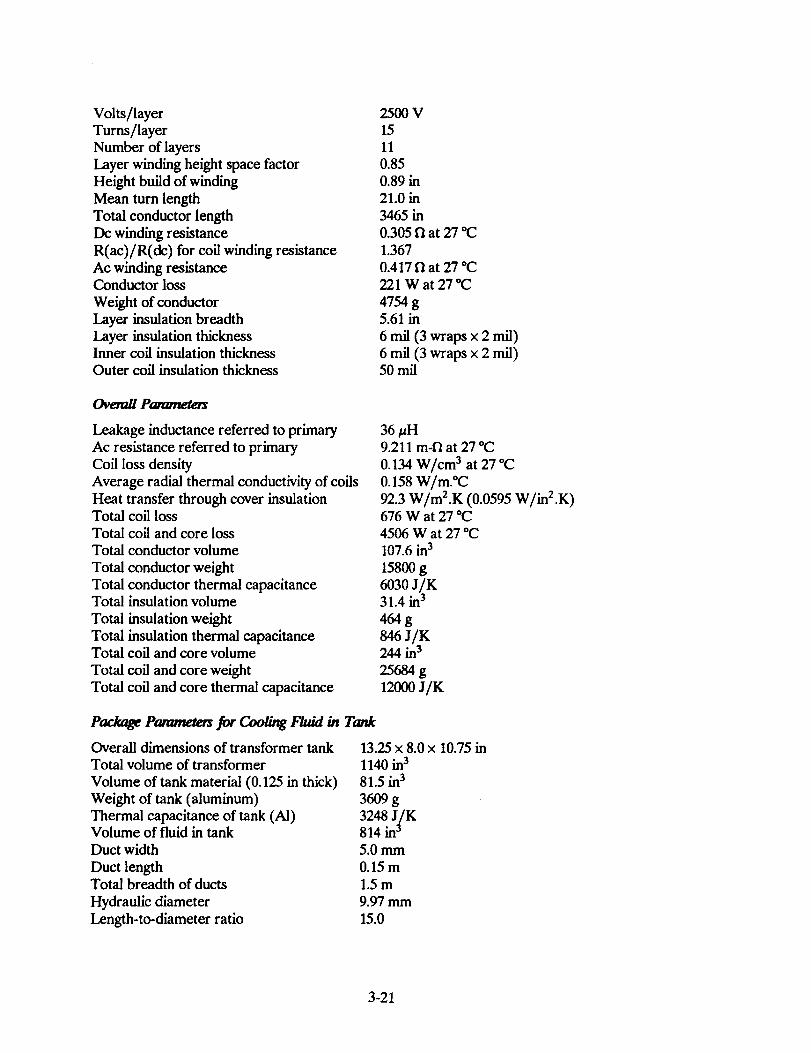
Volts/layerTurns/layer
Number of layers
Layer winding height space factor
Height build of winding
Mean turn length
Total conductor length
De winding resistance
R(ac)/R(dc) for coil winding resistance
Ac winding resistanceConductor loss
Weight of conductorLayer insulation breadth
Layer insulation thicknessInner coil insulation thickness
Outer coil insulation thickness
250O V15
11
0.850.89 in
21.0 in3465 in
0.305 f/at 27 *C
1.367
0.417 fl at 27 °C
221 W at 27 *C
4754 g5.61 in
6 mil (3 wraps x 2 mil)
6 mil (3 wraps x 2 mil)50 nail
Ovem//Parwnetets
Leakage inductance referred to primary
Ac resistance referred to primary
Coil loss density
Average radial thermal conductivity of coils
Heat transfer through cover insulationTotal coil loss
Total
Total
Total
Total
Total
TotalTotal
Total
Total
Total
coil and core lossconductor volume
conductor weight
conductor thermal capacitanceinsulation volume
insulation weight
insulation thermal capacitancecoil and core volume
coil and core weight
coil and core thermal capacitance
36 H9.211 m-f2 at 27 °C
0.134 W/cm 3 at 27 *C
0.158 W/m.°C92.3 W/m2.K (0.0595 W/in2.K)676 W at 27 *C
4506 W at 27 °C107.6 ins
15800 g6030 J/K31.4 in3
464 g
846J/K244 in3
25684 g
12000 J/K
Package Pw'wnae_ for Coo//ng F/u/d/n Tank
Overall dimensions of transformer tank
Total volume of transformer
Volume of tank material (0.125 in thick)
Weight of tank (aluminum)
Thermal capacitance of tank (AI)Volume of fluid in tankDuct width
Duct lengthTotal breadth of ducts
Hydraulic diameter
Length-to-diameter ratio
13.25 x 8.0 x 10.75 in1140 in3
81.5 in3
36O9 g
3248 J_/K814 in °
5.0 mm0.15 m
1.5 m9.97 mm
15.0
3-21

ViscosityPrandtlnumber
8.96E-3g/m.s0.706
Weightof hydrogen
Thermal capacitance of hydrogen
Total transformer weight
Total transformer thermal capacitance
Adiabatic temperature rise (average, 1000 s)
4.36 g
62J/K
26748 g
14035 J/K321 K
Velocity of flow
Reynolds number
Fanning factor, smooth duct
Fanning friction factorStanton number
Heat transfer coefficient
Pressure dropVolumetric flow
Mass flow
Blower power
Fluid temperature rise
Inlet temperature
Outlet temperature
Average surface temperature rise
30 m/s10926.
7.55E - 03
7.77E - 03
3.05E - 03
429 W/m2.K (0.277 W/in2.K)
68.9 N/m E (10E-3 lb/in 2)
0.225 m3/s (477 CFM)
73.7 g/s
15.5 N.m/s = W4.3 K
298 K
302 K
23.4 K
Core surface temperature rise
Core hot-spot temperatureHeat transfer through coil cover & surface
Coil cover and surface temperature rise
Coil hot-spot temperature rise (from bulk gas)
Coil hot-spot temperature
Coil average temperature
Loss multiplier due to increase in resistance
Coil loss at average temperature
Total transformer loss at average temperature
66 K
391 K (118 °C)75.9 W/m2.K (0.0489 W/in 2.K)28K
114 K
414 K (141 °C)
385 K (112 °C)1.34
906W
4736 W
S_
The temperature rise calculations are for continuous operation at full power. In view of
the orbital duty cycle of 18.5%, the results are conservative. The temperature can be reducedby lowering the inlet temperature of the cooling fluid. In the case of oil cooling, this strategy
is limited by a significant increase in its viscosity. Also, the heat transfer can be improved by
increasing the fluid flow rate, if necessary.
The change from oil to hydrogen cooling increases the core hot-spot temperature from 62
to 118 °C, but the latter is still below the limit of 150 °C for Metglas 2605S-3A material. The
increase in the coil hot-spot temperature from 135 to 141 °(2 is much less, because the poorthermal conductivity of the coil and high-voltage cover insulation is much more significant in
determining the temperature rise.
In the case of oil cooling, if it is assumed that the weight of liquid surrounding the rectifier
and filter capacitors (which are also oil cooled in this concept) and in the oil-to-hydrogen heat
3-23
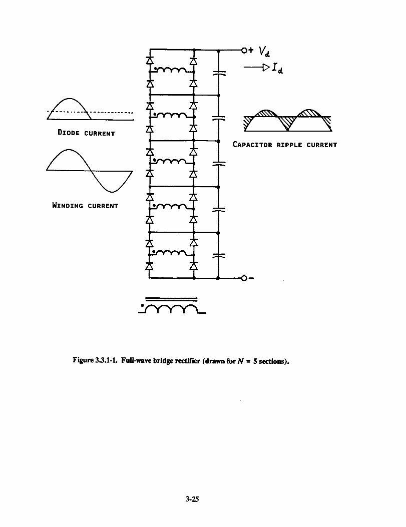
DZODE CURRENT
I_ZNDZNG CURRENT
2" 2,fy-y..y..__
2
i 2
II
I
CAPACZTOR RZPPLE CURRENT
illI nu
Figure 3.3.1-1. Full-wave bridge rectifier (drawn for N = 5 sections).
3-25
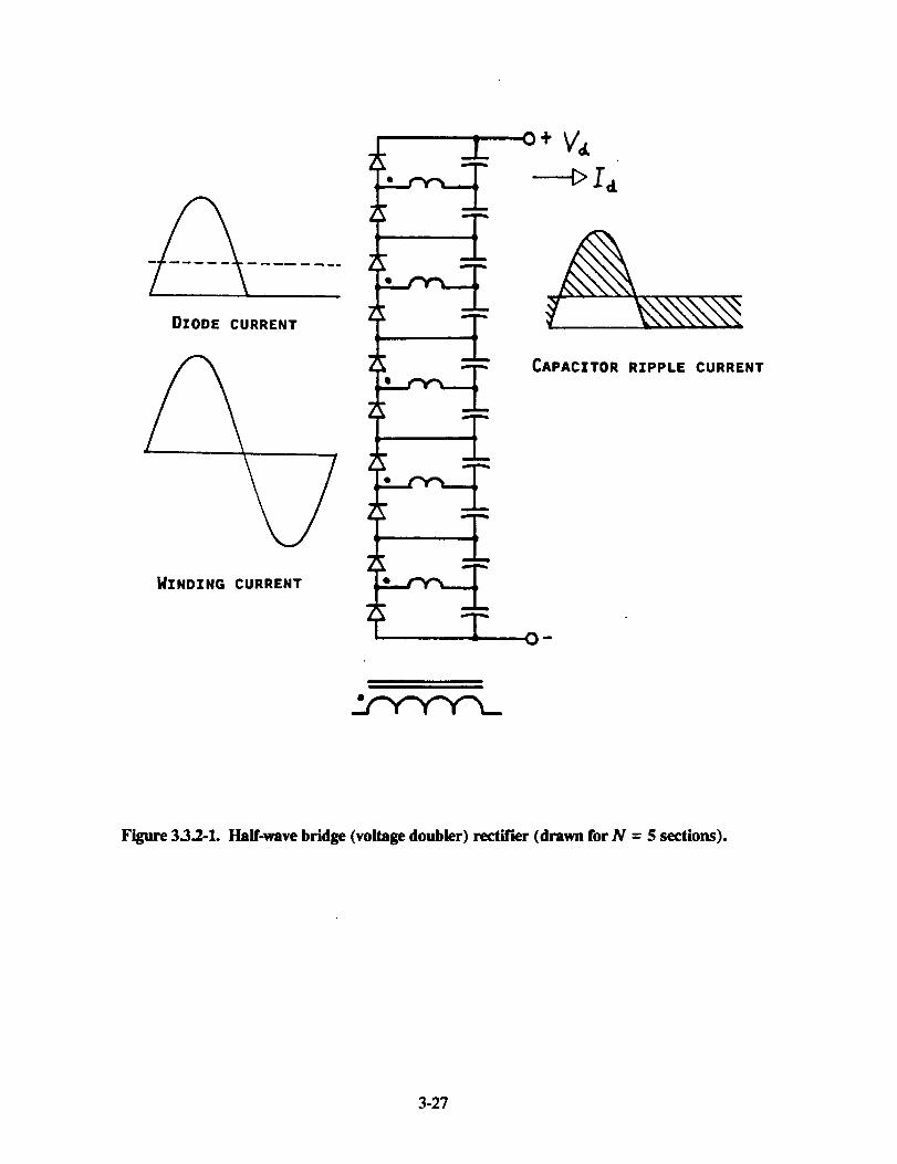
DZODE CURRENT I
tCAPACZTOR RZPPLE CURRENT
WZNDZNG CURRENT
Figure 3.3.2-1. Hag-wave bridge (voltage doubler) rectifier (drawn for N = 5 sections).
3-27
_r Modu/_
The 80-nF, 100-kV de filter capacitor will be divided into 22 series sections of 1.76 t_F,
4.55 kV each. The total capacitor weight is estimated to be 14 kg, and the total loss 60 W. The
capacitors will be manufactured by Maxwell Laboratories, and some details are given in Sec-tion 4.4.6.
3.4 Resonant Component Designs
3.4.1 Resonant Inductor Design
The series resonant inverter proposed for the 1-MW inverter requires that a resonating in-
ductor be placed in series with the resonating capacitor and the transformer primary. The
electrical parameters of this inductor are
Inductance 300 #H
Current (worst case) 235 Arms (at 22 kHz)
Peak voltage 18800 V (at 1 MW load)
Q > 500
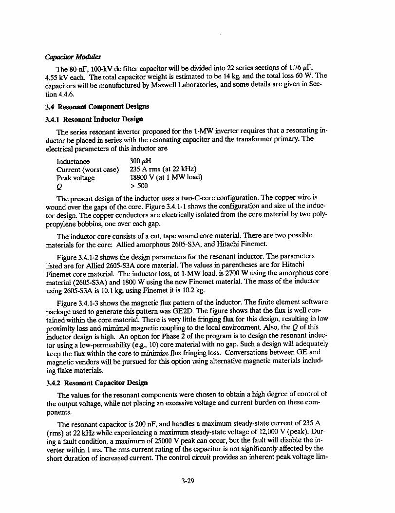
The present design of the inductor uses a two-C-core configuration. The copper wire iswound over the gaps of the core. Figure 3.4.1-1 shows the configuration and size of the induc-
tor design. The copper conductors are electrically isolated from the core material by two poly-
propylene bobbins, one over each gap.
The inductor core consists of a cut, tape wound core material. There are two possible
materials for the core: Allied amorphous 2605-$3A, and Hitachi Finemet.
Figure 3.4.1-2 shows the design parameters for the resonant inductor. The parameterslisted are for Allied 2605-$3A core material. The values in parentheses are for Hitachi
Finemet core material. The inductor loss, at 1-MW load, is 2700 W using the amorphous core
material (2605-$3A) and 1800 W using the new Finemet material. The mass of the inductor
using 2605-$3A is 10.1 kg; using Finemet it is 10.2 kg.
Figure 3.4.1-3 shows the magnetic flux pattern of the inductor. The finite element software
package used to generate this pattern was GE2D. The figure shows that the flux is well con-tained within the core material. There is very little fringing flux for this design, resulting in low
proximity loss and mimimal magnetic coupling to the local environment. Also, the Q of this
inductor design is high. An option for Phase 2 of the program is to design the resonant induc-
tor using a low-permeability (e.g., 10) core material with no gap. Such a design will adequately
keep the flux within the core to minimize flux fringing loss. Conversations between GE and
magnetic vendors will be pursued for this option using alternative magnetic materials includ-
ing flake materials.
3.4.2 Resonant Capacitor Design
The values for the resonant components were chosen to obtain a high degree of control of
the output voltage, while not placing an excessive voltage and current burden on these com-
ponents.
The resonant capacitor is 200 nF, and handles a maximum steady-state current of 235 A
(rms) at 22 kHz while experiencing a maximum steady-state voltage of 12,000 V (peak). Dur-ing a fault condition, a maximum of 25000 V peak can occur, but the fault will disable the in-verter within 1 ms. The rms current rating of the capacitor is not significantly affected by the
short duration of increased current. The control circuit provides an inherent peak voltage lim-
3-29
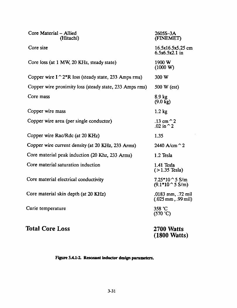
Core Material - Allied
(Hitachi)
Core size
Core loss (at 1 MW, 20 KHz, steady state)
Copper wire I ^ 2*R loss (steady state, 233 Amps rms)
Copper wire proximity loss (steady state, 233 Amps rms)
Core mass
Copper wire mass
Copper wire area (per single conductor)
Copper wire Rac/Rdc (at 20 KHz)
Copper wire current density (at 20 KHz, 233 Arms)
Core material peak induction (20 Khz, 233 Arms)
Core material saturation induction
Core material electrical conductivity
Core material skin depth (at 20 KHz)
Curie temperature
Total Core Loss
2605S-3A
MEa3
16.5x16.5x5.25 cm6.5x6.5x2.1 in
1900 W
(1000 W)
300 W
500 W (est)
8.9 kg(9.0 kg)
1.2 kg
.13 cm^2
.02 in ^ 2
1.35
2440 A/cm ^ 2
1.2 Tesla
1.41 Tesla
(> 1.35 Tesla)
7.25"10 ^ 5 S/m
(9.1"10 ^ 5 S/m)
.0183 mm, .72 mil(.025 ram, .99 rail)
358 'C
(570 'C)
2700 Watts(1800 Watts)
Figure 3.4.1-2. Resonant inductor design parameters.
3-31
itation on the resonant capacitor. The maximum capacitor fault voltage can be reduced below
the 25 kV (peak) through the design of the control section.
3.4 Control System Design and Simulation
The anticipated applications of these high-power converters involve two major modes ofcontrol:
1. De voltage regulation with current limit, for ordinary power supplies to feed variable-current loads.
2. De current regulation with voltage limit, for charging energy-storage capacitors used in
pulse-forming networks (PFNs).
To obtain either mode of control, we expect to use both frequency modulation and phase con-
trol (pulse-width modulation) for the resonant inverter.
One of the main issues with this converter is the very high voltage (100 kV) at the output.
Sensing this value can be accomplished by a frequency-compensated voltage divider. This
lower level signal will require isolation before it can be connected to the integrated control
circuit. With a system power rating of up to a megawatt, current limit is necessary to prevent
damage caused by high-voltage arcs and fault currents.
3.4.1 Series-Resonant Circuit Characteristics
The circuit topology for this report is a series super-resonant inverter, so named becausethe frequency of operation is always greater than the resonant frequency. Series super-
resonant circuit operation has the advantages that no power switch turn-on loss occurs, loss-
less capacitive snubbing can be used, and overall circuit efficiency is high. Reduced electricalstress on the semiconductor devices and reduced EMI occur because of the near-sinusoidal
current waveform. Figure 3.5.1-1 shows the circuit schematic and the component values. The
circuit switches at high frequency in order to reduce the size and weight of the principal com-
ponents.
The circuit is termed series resonant because the resonant inductor (L,_), and resonant
capacitor (C_) are in series with the primary of the high-voltage transformer. The resonantfrequency for the circuit of Figure 3.5.1-1 is 20.5 kHz (1/[L_ *C,_] 1/2) and is an importantcircuit characteristic.
The computer analysis in this section assumes ideal switches. The actual semiconductor
switching device used will be the MCT (shown for simplicity as a bipolar transistor). Each of
the transistors of Figure 3.5.1-1 turns on switches independently. The only constraint on thecircuit is that devices Q1 and Q2 (or O3 and Q4) cannot be turned on simultaneously to pre-
vent shoot-through, a direct conduction path from the de supply bus to common. The voltageacross nodes A and B of Figure 3.5.1-1 can be either + Vrau, -Vra/t, or 0 V, depending on
which combination of transistors or diodes is conducting.
This circuit has three energy storage components: Lres, C_, and Couv The interaction of
these energy storage components is critical to the operation and understanding of the circuit.
Frequency Modulation
The output voltage of the 100-kV filter capacitor is assumed to remain constant during a
single steady-state switching event. This is a valid assumption, as shown by the maximum ca-
pacitor ripple of 0.25% (peak) from the simulation results. The filter capacitor output voltage
3-33
reflects back to the primary of the transformer as + Vcout/N when ILr is positive, and
- Vcout/N when IL,. is negative.
Using frequency modulation, the switch pair Q1 and Q4 (or Q2, Q3) are gated on and offsimultaneously. The pair Ql:O4 remains on for 50% of the time, and Q2:Q3 on for the other
50%. The duty ratio always stays at 50%. The frequency of the gating signals changes to regu-
late the output voltage under different load conditions.
For inverter operation above resonance, an anti-parallel diode (coasting diode) turns on
before its corresponding transistor turns on. This action discharges the snubber capacitor
(not shown in Figure 3.5.1-1) and recovers the capacitor energy. The diode does not need to
be a fast recovery type, and the system exhibits lossless snubbing.
The steady-state operating condition of the series super-resonant inverter sequencesthrough a four-mode cycle. Figure 3.5.1-2 displays these modes. The inverter cycles through
mode 1, mode 2, mode 3, mode 4, mode 1 .... The dark lines show the current path for that
mode. Figure 3.5.1-2 displays the conducting semiconductor devices, the voltage appliedacross the resonant network, and the direction of current.
Figure 3.5.1-3 displays the resonant inductor current and resonant capacitor voltage
waveforms during a 1-MW, steady-state operating condition. The figure displays the conduc-
tion region of each of the semiconductor devices. The output voltage reflects back to the pri-
mary of the transformer as a dc voltage of value + Vco,,t/N or - Vco,,t/N. Using this, and the
polarity of the applied rail voltage (depending upon which semiconductor devices are conduct-
ing), the four conduction modes comprise the resonant capacitor and inductor in series with
four discrete voltage source values. The resulting resonant inductor current and resonant ca-
pacitor voltage consist of sections of sinewaves for each of the four modes. Only the applied
forcing function is changing in a stepwise fashion.
It is important to note that this analysis transforms the initial nonlinear system into a
linear equivalent model. The control method descril_l later uses this linearization property.
Figure 3.5.1-4 displays the equivalent resonant-network circuit. The applied voltage (V,_)
is a variable frecjuency square wave. The figure shows a loss component resistor includingcopper losses, I'R losses, etc. The series resonant network has an output voltage transferfunction shown in Figure 3.5.1-5. The x-axis is the frequency of the applied square wave, and
they-axis is the output voltage. The regulated output voltage is 100 kV for the NASA inverter.
The figure has a horizontal line drawn at 100 kV, with a vertical line at the 20.5-kHz resonant
frequency of the network. Since the network is super-resonant, it always operates to the rightof this vertical line. The applied voltage Vat, is always at a frequency greater than 20.5 kHz. A
locus of four output currents (0.5, 2.5, 5, and 10 A) displays the transfer function of the invert-er for each current.
At high output currents, the slope of the transfer function (AVcout/Afreq) is large. The
100-kV output voltage operating point is at the intersection of the current locus line and the
100-kV line. For super-resonant operation, to keep the output voltage constant, the operating
frequency increases as the load current decreases. For very low current conditions, the switch-
ing frequency is too high for the semiconductor switches. For the 0.5 A load current conditionof Figure 3.5.1-5, the operating frequency of the semiconductor switches would need to be
much greater than 50 kHz. The control system must use another method to regulate the out-
put voltage under low-load current conditions.
3-35
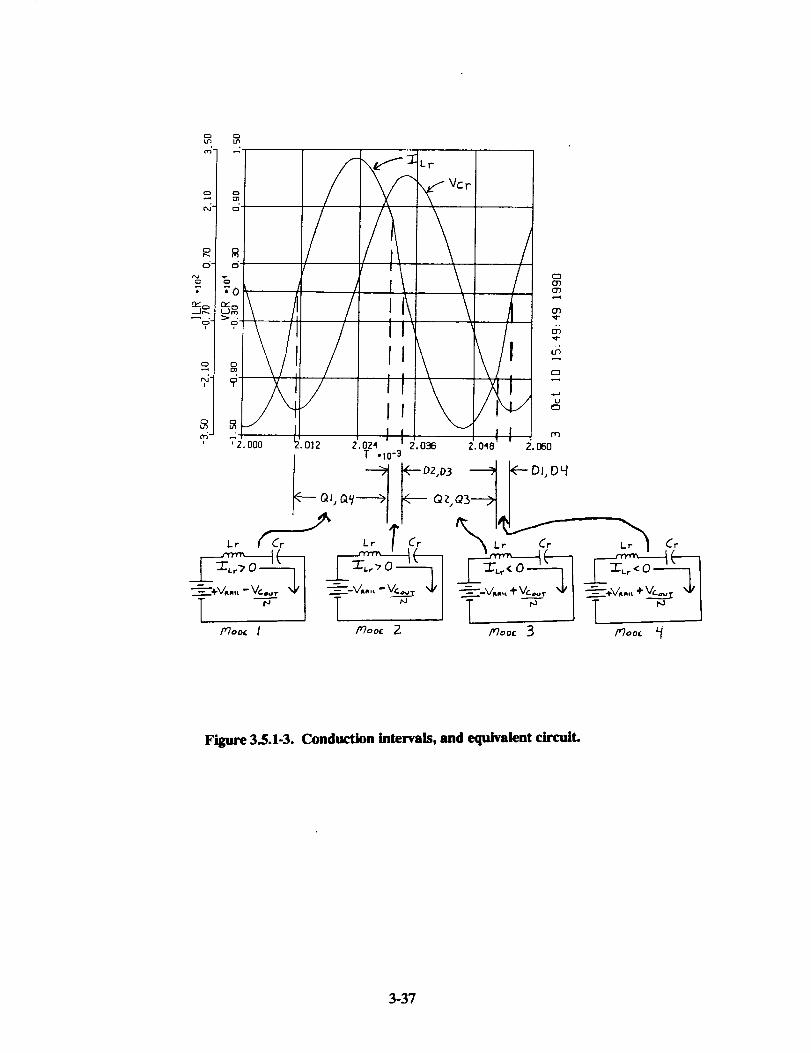
I/3
0
(',F
O"
%
.--Jr-.
,o
l
I'2.OOO
Lr
IrIII i
,O]2 2,024 2.036
O3O3
J | m
2.1360I T ,10-3
Lr _r_ _ Lr _ _r '_ Lr _r
T --"-IT IT -1
Figure 3.5.1-3. Conduction intervals, and equivalent circuit.
3-37
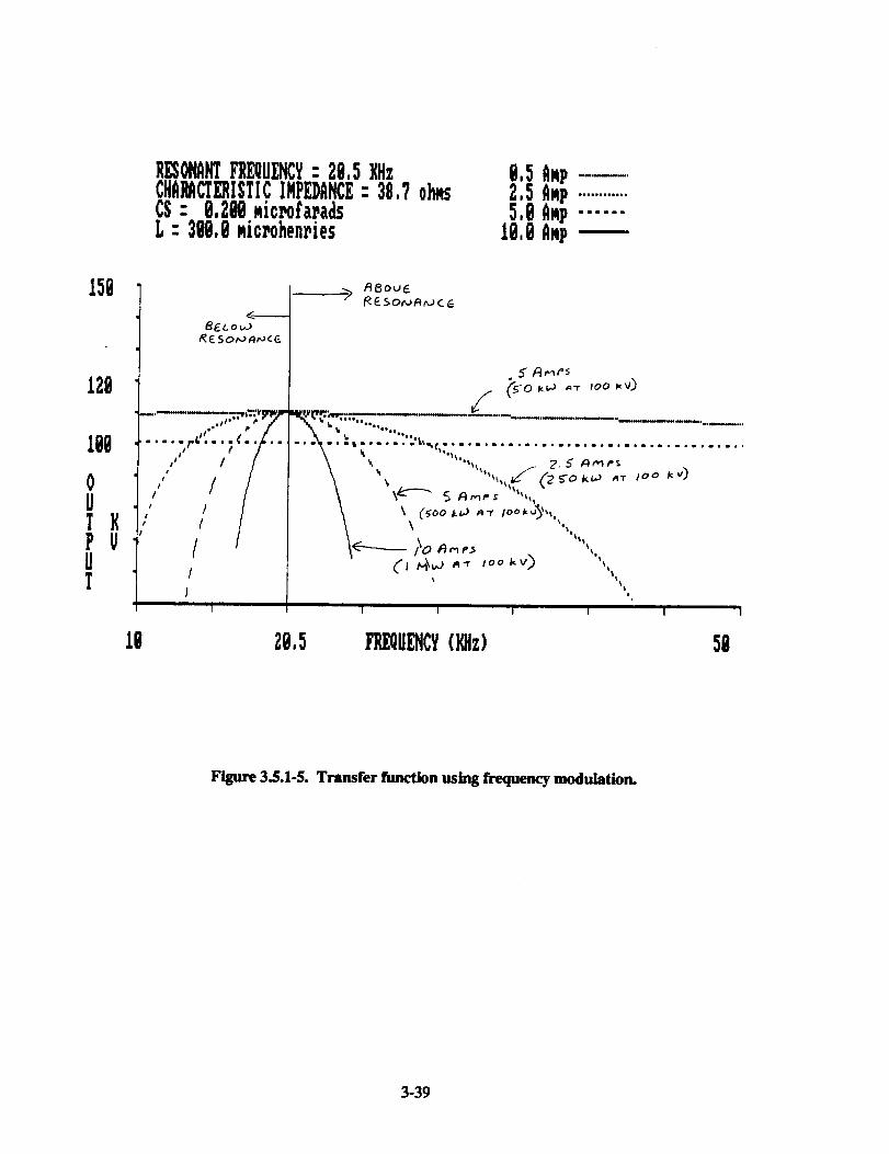
WOI_ I_UENCY: 28,5_zCIIA_CTDISTICIHPDANCF: 38,70h.sCS: 0,2_0,iceota_adsL : 310,1_Jcx,oheneies
0,5 A_p......2,5 Ace........5,8 AMp-_10,0A_p
100
0U
XPUU
_._.__.._ t98O_JE
./_ ("5-ok_ ,-r Ioo J,v)
.-_.. t•..... "_':._.._....... "'"...."k _ _e _ ° I I e I a Ibml_ all I e O I o it Ol _ m _ l
_(-'_-'-- I_0 l:)_e_ '",,.
1050
Figure 3._.1-5. Transfer function using frequency modulation.
3-39
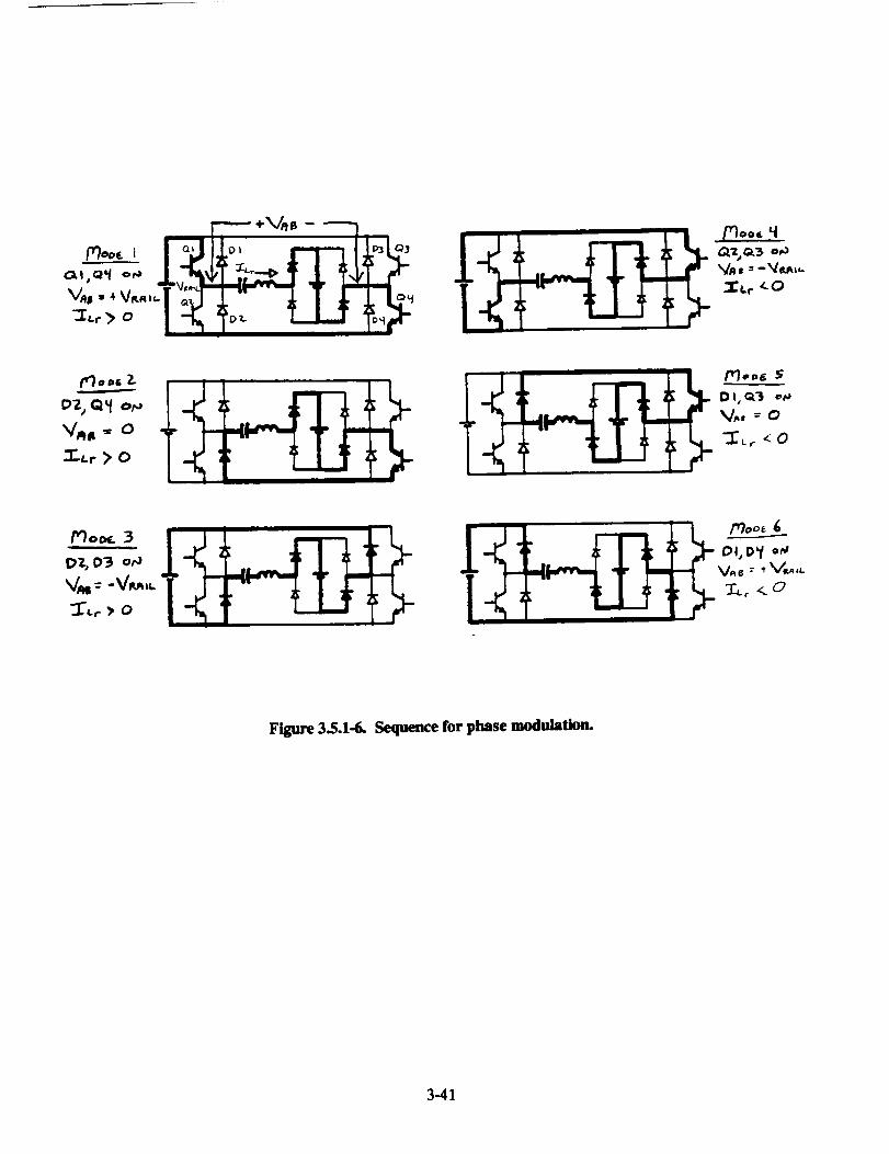
O. l, Q'/ e,_
3:4._ _.0
moo,._,
OZ_ Q_f o_
V, qll = 0
:I-or> 0
/_oo£ S"
DiaQ3 4_#
_/^, = O
_,7.,o3 #,.,V, = -V,.,,,_._Cr > 0
DI, Dif o_
Figure 3.5.1-6. Sequence for phase modulation.
3-41
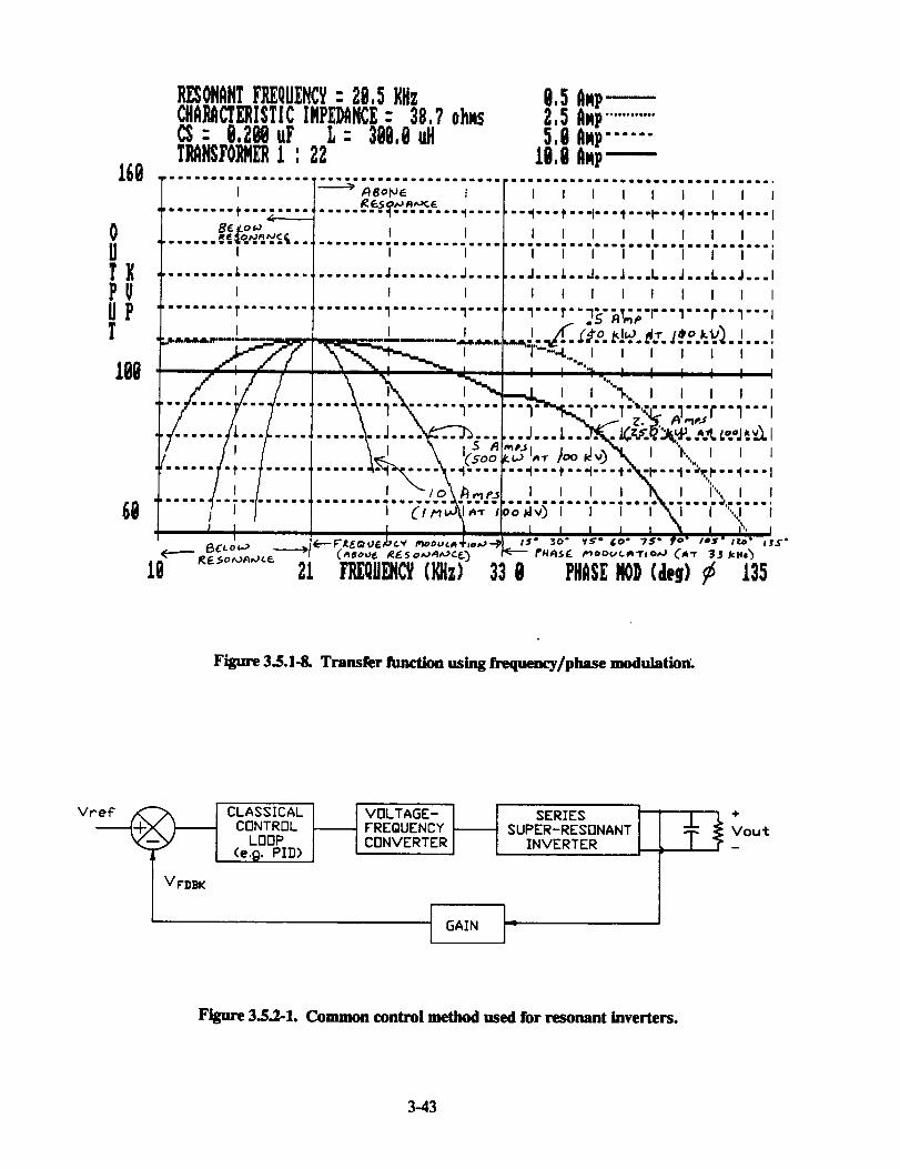
168
ommmmBuu_m_mmmwue
8¢to_
!1 iTK .......- - +..........PUUP ......... '+"'"t _.............._L_
i t¢._..._ BfLo _-_
1@
O0,O,,, ,UENC,"2,,, i!+_A_ISTIC IMPDANCE: 38,? 0h.s Axp............
CS- 6,280 uP L- 388,8uH _ A.pT_HSFORM_1:22 1 A.p
........... ._ ,+;;,.,;ii • Iiii imm i i i i I i II iiii Ii i i i i +llllll lllll ii llllllll i I II iiii IIIiiii i
I I I I I l I I I I
........ _ ........ _ ....... "I"""I'"" "l"- - i'---l'--.l---l,' - - 4 --- I
I II |I| iI nit• mile |mmI|aa mmm
I I
...... ... J ........ J ....
I I
, mmm I In +! ii mmmomm _mlmmm mmm lmmoe
I I I I I I I I I
... J... L...I...I...L.. J...L.. J... I
I I I I I I I I I
............... 'I........ "i....... _"" T-" 2y ;_;-r-- l---r-- _--- iI I I ]f (#o _I_> 4,..c leo k.U_ I I
,._-r_=_:.-----_.._-+_.,_.= ........................../-/ \-'--,_.-_.._._ ---.,... I , , , i , ,-- ". "-_ -- ' I I ""I, I I I I I I
i \ \ ,.-....,..,_ ,,, ,r----:-----,C--_-%..... -_...... _.-,_-,--_:-_-.... J...... _.. J... _ ...... J.. -,_i _._._...._. _.;_._._,e..,.,L _o.oj_.,2.I
5 FI ,,_+uC %,
.... '_...... "'"I "_ .... 't" "I.... :'"" "1""" f " " "1-- = i' ="_k_'p"""1""+,pp"" "1"- - I
............I-- .... I:',.'...---i/ _ .... _ I _...u .L..L .L._ , ;",
._.__..e_+_-...--_'+t_u_hc.,, ' _ooo+.++-l-,o,,.,-._l_ _:r _o" Y_" _o- 7_r fo* o.$-_- _+.--
21 P]EQUEHC£(EHz) 338 PHAS!I+0D(aeg)_ 135
Figure 3.5.1-8. Transfer function using frequency/phase modulation.
._ CLASSICAL { VOLTAGE- l
CONTROL -- FREQUENCY --LBBP CONVERTER
(e,_, PID)
V FDBK
I GAIN
SERIES ISUPER-RESONANTINVERTER
J
Vou'l:
Figure 3.5.2-1. Common control method used for resonant inverters.
3-43
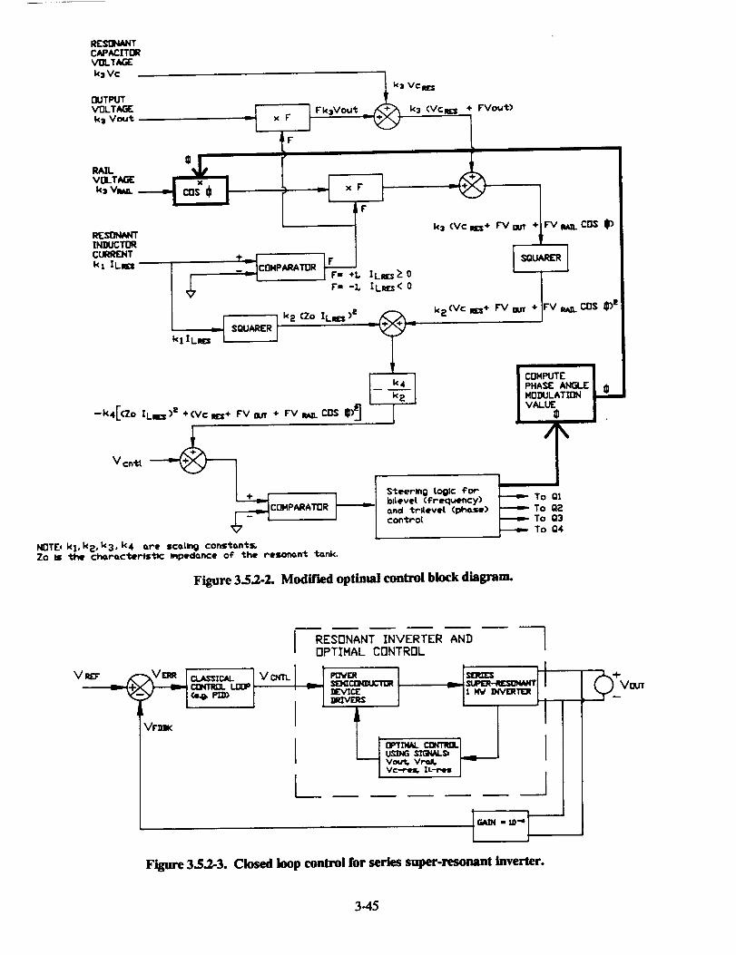
F'- -L ILRrJ< 0
Figure 3.5.2-2. Modified optimal control block diagram.
(e4> PI_) J
Vr:=K
Iv=_.[
i
RESONANT INVERTER AN])OPTIMAL CONTROL 1
] =-_.. I I=,== t]so_caN_cr_ I _!=u=t__l I=L"V;OE I v I1 NV _IVE:RTOt I
=7' ' I/ w-,-_ z--,_ 1
L____ __J
Figure 3.5.2-3. Closed loop control for series super-resonant inverter.
3-45
Lr Cr RLoss
ILr_ -kVCr -
-I- _-
VQB
1.Nt-t-
V Cout C out RloQd
STATE EQUATIONS
iLr-- [i/Lr] FV&ppt-Vcr
_/Cr = [I/Cr] [I Lr ]
Vcout= [I/Cout ] [ABS(ILr)/N -
NDTE, This system Is non(Inear due to
-I Lr _R Loss-Sign(I Lr)_VCou_/N]
V Cout/R [o_
the ABS nnd Sign _unc±lons,
Figure 3.5.3-1. Inverter and state equations.
3-47
Ip).
_8
RES CAP VOLT, RES IND CURR, APPL VOLTAT ] MW, FREO=22.2KHZ
II
II
lj
iI
II
U
• I
I
° I
\
II
T
*O
c__
c_
III II
II
r_
oc3.._;,'2. 000 2. 120
Im
2.040 2.060 2.080 2.I00T ,10-3
Figure 3.5.3-4. Inverter waveforms - 1-MW load.
3-49
CD0
.=dI
c_o
!
oo
TC_
mt_<E
c_
RE$ CAP VOLT. RES IND CURR. APPL VOLTAT 100 KW. FREO=33KHZ
0
c5
C_
uE:)
cr)
' 6.000 6.020 6.040 6.060 6.080 6.100T o10-3
Figure 3.53-7. Inverter waveforms - 100-kW load.
3-51
ure 3.5.3-9. The implementation of the short-circuit protection is to place a limit (i.e., a
clamp) on the control signal of the modified optimal control (Figure 3.5.2-2). The magnitudeof the short-circuit current depends upon the clamp value. This limit controls the maximum
output current delivered under a fault condition and the stress placed on the inverter electron-ics.
Figure 3.5.3-9 shows the system response when powered to a 1-MW steady-state condition
(Rtoad = 10K). A "short-circuit" load condition, simulated by a 1004-1 load resistance, is ap-
plied at 3.5 ms. The 100-fl short-circuit value was chosen to be 1% of the smallest operatingload (1 MW corresponds to 10000 n). Choosing a resistance value less than this does not alter
the output current or electrical stress to a significant extent. The commanded voltage refer-ence remains at 100 kV, however, the inverter control limits the output current to approxi-
mately 20 A at a reduced output voltage of 2 kV. The inverter can continue to operate at this
output short-circuit condition for several milliseconds without damage to any components.
The control limits the peak capacitor voltage and inductor current. However, the circuit mustbe disabled before the components heat up beyond their rated specifications.
Figure 3.5.3-10 displays the resonant capacitor voltage and resonant inductor current for
the short-circuit condition of Figure 3.5.3-9. The initial transient (0 to 0.6 ms) occurs during
the interval when the control is bringing the output voltage up to 100 kV. At 3.5 ms theshort-circuit fault occurs. The current and voltage is bounded to a larger value. The magni-
tude of the voltage and current during the short circuit is controlled by the clamp value placedin the control circuitry. The inverter control circuit (i.e., low voltage, low power electronics)
provides this short-circuit protection; no high-power protection circuit is needed to protect theinverter and its components during this fault. The fault eventually must be removed, or the in-
verter must be disabled before the inverter components overheat, but the circuit has a rela-
tively long time interval (i.e., several milliseconds) before this would occur.
3.6 System Protection
The converter system must be protected against load faults, source faults, and internal
converter faults. The most critical component of the converter to be protected is the semicon-
ductor switch module, which is also the component most capable of rapid response to fault
conditions. The control circuit of the inverter switches will incorporate as many features aspossible, such as current limiting, automatic shutdown, and careful restarting, to protect the
load and source as well as self-protection of the switches. This will be the first line of protec-
tion, and should be sufficient for the load, assuming it is not regenerative.
The second line of protection will be the de input circuit fuse. For a 1-MW convertermodule, the fuse must be rated for 5 kV, 200 A, and must operate as fast as possible. The dc
input filter inductance will limit the rate of rise of fault current, but the steady fault currentwill be determined by the characteristics of the de source. The minimum function of the fuse
will be to isolate a failed converter module. The desired function will be to protect the MCT
switches in case of misfire or accidental conduction of a pair of switches in the same phase leg
(shoot-through).
Typical high-voltage loads are subject to short-circuit faults, and might be damaged by
discharge of the output filter capacitors, which store 400 J in our present design. For protec-
tion, a crowbar consisting of a triggered spark gap is proposed. This equipment will be sup-
plied by Maxwell Laboratories, and the arrangement is described in detail in Section 4.4.7.
The weight is estimated to be 1.84 kg.
3-53
3.7 Cooling System
A scheme for direct hydrogen cooling of the entire converter system is outlined in Fig-ure 3.7-1. The components are mounted within a common, thin-waned enclosure containing
hydrogen under a static pressure of about 4 arm, which need not be maintained when the con-
verter is not operating. However, it is assumed that the temperature is maintained within a
range between about 270 and 310 K ( -3 *(2 to 37 °C), compat_le with the optimum storage
temperature of all components, under standby conditions.
In operation, hydrogen is blown through the enclosure to cool the components, maintain-ing a continuous circulating loop (Figure 3.7-1). As the gas becomes heated above a certain
temperature limit (310 K, for example), some of it is exhausted from the outlet end of the sys-
tem and replaced by injecting fresh liquid hydrogen at 20 K into the cooling loop. The fresh
hydrogen is evaporated and mixed with the circulating flow to reduce the inlet temperature to
a certain lower limit (270 K, for example). The blower may be located at either the inlet end,
as shown in the figure, or at the outlet end. Appropriate temperature and pressure controls
are provided for the blower and the inlet and outlet valves.
In steady-state operation, the amount of hydrogen injected as a liquid at 20 K is equal to
the amount exhausted as a gas at 310 K. This allows all the enthalpy of hydrogen over this
temperature range to be utilized for cooling the converter, minimizing the quantity required.
The average specific heat of gaseous hydrogen over this temperature range is about12.75 J/g.K, so the heat absorption capacity is
Qgas = (310 - 20)x 12.75 = 3697 J/g
To this, the latent heat of vaporization (1831 J/g) can be added:
Qtotca = 3697 + 1831 = 5528 J/g
The hydrogen mass flow required for continuous operation is then
3600H2 flow - 5528 = 0.65 kg/kWhtoJs
= 36 kg/h for 56 kW loss
In the gas circulating loop, the specific heat of hydrogen at the average temperature of290 K (17 °C) is 14.3 J/g.K, so the heat absorption capacity from 270 K to 310 K is
Qtoop = (310 - 270) x 14.3 = 572 J/g
The hydrogen mass circulating flow required is then
1H2 circulating = 57----2g/Jtoss
= 98 g/s for 56 kW loss
The blower power required to maintain this flow is estimated to be about 1 kW. The particu-
lax temperatures assumed in these calculations may be modified to optimize the operating
temperatures of the components.
3.8 Summary
The design of the high-voltage transformer-rectifier has been established. A core-type
structure employing two coils, one on each leg of a C-core, has lower weight than the alterna-
3-55

tive shell-type structure, with a single coil on one leg of the core, or on the center leg of an E-
core. The primary windings are connected in parallel, which balances the flux in each leg. A
special interconnection between the secondary windings and the rectifier and filter is neededto minimize reflected capacitance at the primary side. The secondary windings are divided
into sections, each consisting of a single layer from each coil connected in series, and each
feeding a section of the rectifier. By making series connections of these sections on the dcside, the interlayer voltage is purely de (equal to the output voltage divided by the number of
sections). Thus, the charge on the interlayer capacitance does not have to be cyclically re-
versed, thereby reducing the effective ac capacitance to a very low value. This is required for
proper operation of the series inverter. A half-wave bridge (voltage doubler) rectifier connec-tion has been selected because it can be built with fewer sections or layers (11 in the proposed
design) than a full-wave bridge. This reduces the amount of layer insulation and the number
of leads required, as well as the number of diode modules.
Some type of amorphous metal (Metglas or Finemet) will be used for the core. While our
present design uses Metglas 2605S-3A operating at about 1 T, this is subject to more detailedevaluation of materials and the variation of core loss with flux density. A critical factor in
minimizing transformer weight is achieving a high conductor-to-insulation space ratio, espe-
cially in passing through the core window. Both primary and secondary windings will employ
copper conductors of rectangular compacted litz wire, needed at 20 kHz. The high-voltage
secondary windings will be completely enclosed within solid insulation forms of a material
such as polypropylene, across which a very high voltage gradient can be allowed. Sections ofthe coil forms must fit together very tightly so that the high-gradient electric field is contained
within the assembly, allowing close spacing to the core and nearby grounded structures. Toremove the heat generated by losses when operating at high core flux density and high coil
current density, cooling ducts will be provided in the structure, except in the core window.
In our original concept, the rectifier diodes and de filter capacitors were to be enclosed
with the secondary windings in extended forms of polypropylene insulation, and the assembly
mounted together with the resonant inductor in an aluminum tank filled with oil for insulation
and cooling. However, this plan was modified because of the disparity in the heat generation
and temperature limits of these components, and it is now proposed to group the diodes and
capacitors at one end of the transformer. In this arrangement, forced oil cooling will beeffective but the weight of the oil and tank, as well as the weight of an oil to liquid hydrogen
heat exchanger, imposes a severe penalty.
The use of direct gaseous hydrogen cooling is now proposed, eliminating the oil and allow-
ing the tank to be replaced by a lightweight enclosure that includes the inverter and all other
components. Estimates of the heat transfer obtainable with this system show that it is feasibleand should save much weight, but the effect on the dielectric insulation system requires fur-
ther study. At 4 atm, the breakdown voltage of hydrogen is about 50 kV/cm. Since thedielectric constant of hydrogen (1.0) is less than that of the oil (2.55) or the solid insulation
(2.3), it will experience a higher electric field gradient. Reducing the electric field gradient re-quires a somewhat larger core and coil but the overall weight should be less than for an oil-
cooled system.
The estimated weight and losses of the converter system components are listed in Table3.8-1. The overall converter system efficiency is estimated to be 94.4%. To remove the 5.6%
losses, hydrogen flow at 36 kg/h is required when operating at full power.
The resonant inductor design operates at a peak flux density of 1.2 T for the 1-MW load
condition. The design of this core uses a C-C core configuration, which reduces stray flux and
3-57
3.9
[1]
References
R. Oruganti and F.C. Lee, "Resonant Power Processors," IEEE Trans. Ind. AppL VoLIA-21, No. 6, 1985, "Part I - State Plane Analysis," pp. 1453-1460, "Part II - Methods of
Control," pp. 1461-1471.[2] R.J. King and T.A. Stuart, "Modelling the Full-Bridge Series Resonant Power Con-
verter," IEEE Trans. Aerosp., VoL AES-18_ No. 4, 1982, pp. 449-459.
[3] W. McMurray, "The Thyristor Electronic Transformer - A Power Converter using aHigh Frequency Link," IEEE Trans. Ind. AppL, VoL IGA-7, No. 4, July/August 1971,
pp. 451-457.
[4] F.G. Turnbull and ILE. Tompkins, "Design of a Pulsewidth Modulated Resonant Con-verter for a High Output Voltage Power Supply," IEEE Trans. Ind. AppL, VoL IA-23,
No. 6, 1987, pp. 1016-1021.
[5] R.L Steigerwald, "A Comparison of Half-Bridge Resonant Converter Topologies,"IEEE Trans. Power Electronics, VoL PE-3, No. 2, 1988, pp. 174-182.
[6] R. Oruganti, J.J. Yang, and F.C. Lee, "Implementation of Optimal Trajectory Controlof Series Resonant Converter," Conf. Rec. IEEE-PESC, 1987, pp. 451-459.
[7] RJ. King and T.A. Stuart, "Inherent Overload Protection for the Series ResonantConverter," IEEE Trans. Aerosp., VoL AES-19, No. 6, 1983, pp. 820-830.
[8] P.L Doweli, "Effects of Eddy Currents in Transformer Windings," Proc. lEE,VoL 113, No. 8, August 1966, pp. 1387-1394.
[9] E.C. Snelling_ So]t Ferrites - Properties and Applications, Second Edition, London, Eng-land: Butterworth & Co., 1988.
[10] "High-Frequency Ferrite Power Transformer and Choke Design Series," Philips Tech-nical Publications 205-208: Part 3. Transformer winding design (207).
[11] M.M. EI-Missiry, "Current Distribution and Leakage Impedance of Various Types ofFoil-Wound Transformers," Proc. IEE, VoL 125, No. 10, October 1978, pp. 987-992.
[12] P.D. Evans and K.H. A1-Shara, "Losses in Foil-Wound Secondaries in High-FrequencyTransformers," IEEE Trans. Magnetics, VoL 25, No. 4, July 1989, pp. 3125-3132.
[13] "Hitachi New Soft Magnetic Materials 'FINEMET'," Hitachi Metals, Ltd., YA-88O901.
[14] H. Fukunaga, T. Eguchi, K. Koga, Y. Ohta, and H. Kakehashi, "High Performance
Cut Cores Prepared from Crystallized Fe-Based Amorphous Ribbon," IEEE Trans.
Magnetics, Vol. 26, No. 5, September 1990, pp. 2008-2010.
[15] M. Jakob, "Influence of Nonuniform Development of Heat Upon the TemperatureDistribution in Electrical Coils and Similar Heat Sources of Simple Form,"
Trans. ASME, VoL 65, 1943, pp. 595-605.
[16] T.J. Higgins, "Formulas for Calculating the Temperature Distr_ution in ElectricalCoils of General Rectangular Cross Section," Trans. ASME, Vol. 66, 1944, pp. 665-
670.
[17] A. Rele and S. Palmer, "Cooling of Large Transformer Cores," Trans. IEEE,VoL PAS-91, No. 4, July 1972, pp. 1527-1535.
3-59

Section 4
RESONANCE TRANSFORMER-BASED SYSTEM
(Maxwell Laboratories, Inc.)
4.1 Introduction
The high-power, high-voltage dc-dc converter program is intended to provide a power sys-
tem for a variety of future high-power, space-based applications. The specifications describe
a system that is well beyond the established state of the art for power converters. The factthat this system will operate in a space environment also has a strong influence on these
specifications. System weight, cooling, and reliability are examples of parameters whose im-
portance is magnified in a space-based power system of this power level. As a result, the sys-
tem proposed to meet these requirements is different in many respects from conventional
power converters.
Among the salient features of the resonance transformer-based system are
- The inverter uses MCTs as the switching element, which lowers the device count and the
losses compared with other devices at the operating frequency of 50 kHz.
- The voltage step-up is accomplished by a resonance transformer, a Maxwell-patented
resonant circuit. This circuit requires no magnetic materials, allowing for operation at
higher inverter frequencies and for a simpler cooling scheme than conventional systems.
- The Maxwell capacitors used in the system have power densities well beyond that com-
mercially available today.
- A regulator circuit developed at Maxwell provides output voltage regulation of _ 0.25% or
better with a bandwidth of greater than 1 MHz, and weighs less than 3 kg.
These features allow the resonance transformer-based system to meet or exceed the
specifications desired for this program. This approach will also be shown to scale up to higher
power densities as the output power level increases.
4.2 System Specifications
The requirements for the system are
Input voltage
Output voltage
System mass
Duty
Fault energy to load
5 kV de
100 kV dc _+0.25%
< 100kg
> 1000 s continuous operation
"a few tens of joules"
4.3 Critical System Issues
4.3.1 System Weight
The weight of the system is the most critical parameter of those listed above because it is
the most difficult to meet. The power density of 0.1 kg/kW is well beyond the state of the art
for current systems at this power level. The techniques used to meet this requirement include
the use of cryogenic cooling of components, a new generation of high power density capaci-tors, a resonant voltage step-up circuit, a proprietary regulator design, and components espe-
4-1
that fault current. Fusing was chosen because fuses can be made much lighter than dc inter-
rupters at this power level. While interrupters can operate repeatedly without replacement, it
is questionable whether or not this is an advantage for this system. In a high-power systemsuch as this one, the problem that originally caused the fault will most likely still be present in
the system after the fuse or interrupter clears the fault, which means that repairs must be per-
formed before the system is operational again. The fuse can be replaced when the rest of the
system is repaired. For almost all forseeable fault scenarios, a fused disconnect has all the
features of adc interrupter, with the advantages of faster, more reliable operation and lighter
weight.
A terrestrial 5-kV, 200-A fuse would be approximately 12x 12x 6 in and would weigh more
than 20 kg. This is unacceptably large and heavy for this system. Fortunately, the size and
weight of the fuse can be reduced by cooling the conducting dement. Liquid nitrogen cooling
of wires has been investigated by Gilmour et al. [1] for fusing and current-limiting applica-
tions. The cryogenic liquid is boiled off the conductor by the heat generated in the conductor,
forming a gas jacket around the wire and maintaining a constant temperature on the outsideof the wire. At a certain critical temperature, the boil-off mechanism cannot remove the heat
from the wire quickly enough to maintain the temperature in the wire. The wire then quicklyoverheats and fuses. This mechanism produces a current-limiting fusing action which is more
than adequate to prevent the draining of the power source and fault current damage of the
system.
4.3.7 Fault Protection
Protection of the load when a load fault occurs is a requirement for most power systems.
For a 1-MW system that has an allowable fault energy of a few tens of joules, the fault protec-
tion circuitry must be triggered within a few tens of microseconds after a load fault occurs.
This places a constraint on the speed of the trigger circuit. Fault protection requirements of
this type are not unusual and a number of methods can provide the required fault protection.One of these is discussed in Section 4.4.
4.3.8 Reliability
Reliability is clearly important in a system that is in space and, as a result, is expensive and
difficult if not imposs_le to repair. In some of the applications discussed for this program,
even a small amount of system downtime is not acceptable; i.e., system availability must be
100%. The reliability of a system that is beyond the current state of the art and that requires
components that have never been built is difficult to gauge. The approach taken to maximize
reliability and availability is to use as few components as poss_le, and to use passive com-
ponents as much as poss_le. The designs of all components and subsystems were performed
with reliability in mind.
4.3.9 System Hardness
This system must operate in a very harsh environment. Depending on the particular appli-
cation, the ambient environment may include any or all of the following: high radiation levels
(ambient and weapon-generated), rapid temperature cycling, intense vacuum UV flux, high-
velocity debris (ambient and weapon-generated), low-density plasma, free radicals such as ox-
ygen and chlorine, and local pollution from the rest of the spacecraft. The power converter
must be hardened against these threats in order for it to be available when needed. The ap-
proach to minimizing problems caused by the environment is to use intrinsically hard com-
ponents to make up the system and to position the system in the spacecraft in a location that
will minimize exposure to the threats.
4-3
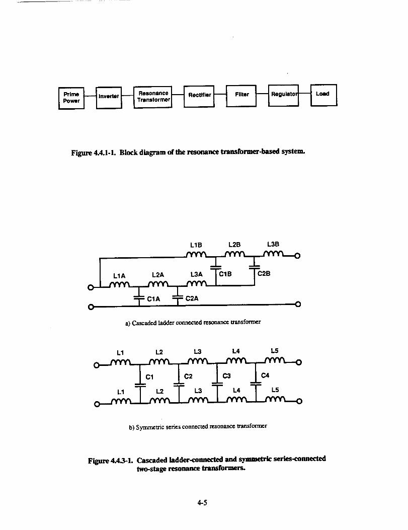
IF,,t.r I_°'rl I.........I I'r'n"°r"rlI H'
Figure 4.4.1-1. Block diagram of the resonance transformer-based system.
LIB 1_2B L3B
' Tc', Tc=_°_a) Cascaded ladderconnected resonance transformer
L1 L2 L3 L4 L5
b) Symmetric seriesconnecP..zlresonancemansforrrcr
Figure 4.4.3-1. Cascaded ladder-connected and symmetric series-connected
two-stage resonance transformers.
4-5
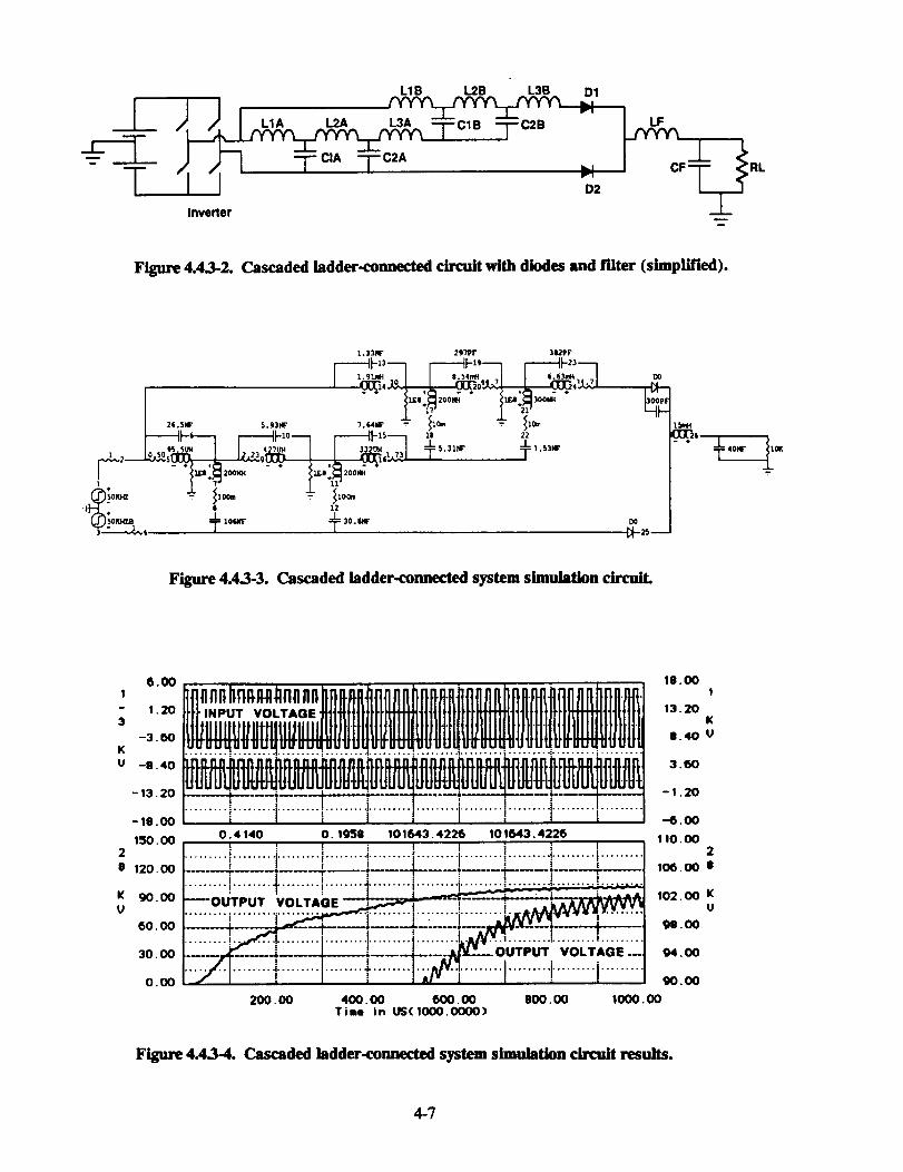
T
LIB L2B L3B D1
/'_ TC B sC2 LF
"_l J/lJ I TCIA TC2A 2 RL
Inverter
Figure 4.43-2. Cascaded ladder-connected circuit with diodes and filter (simplified).
I 26.5W $. 931&-
I---+'--7 r ko-- r--+,,-7
! -"-I _ II 12_) 50_Z_ "!=10_"
W-_---_4 / S 30.
*.331f 29'7PF 31_PF
,8 22
t 5.'tl/_r _ 1. 5311r
[_--aSm
Figure 4.4.3-3. Cascaded ladder-connected system simulation clurculL
6.00
1.20
-3.60
-11.40
- 13.20
-15.00
150. O0
120. O0
90.00
60.00
30. O0
0.00
__ N_U_OI___, ]___'_'__'_i
t'_'- "_" ! .... , .................. i ........ .......... : ......... "......... _ ......... .......... _ .........
0.4140 0.1_$ 101643.4226 101643.4226
I _ s 1 z......... ! ......... l.................. •........................... t .................. ! .........
! _ I ! I t : t !
i I , l _ : ; -
• . z | ° o
......... i ......... I...................... I _ "...... I..........
200. OO
IO.O01
13.20K
O.40U
3.60
- I .20
-6.00
I I0.O02
I06.00 11
102. O0 KU
911,O0
94.00
90,00
400.00 600.00 800.00 1000.00Time in US(1000.0000)
Figure 4.4.3-4. Cascaded ladder-connected system simulation circuit results.
4-7
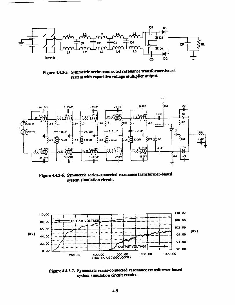
T
C_ D1
inverter I I v,C6 D2
Figure 4.4.3-5. Symmetric series-connected resonance transformer-based
system with capacitive voltage multiplier output.
26._W 5.9,._F
--2h1 - ÷
: 10 _',.'T
5.93l'¢
1.33NF
_°°_ i
297PF 382PF
1EB_ 2oo_ ',',1E8
t T
lg8
1£8 _lO_ "T
Figure 4.43-6. Symmetric series-connected resonance transformer-based
system simulation circuit.
[kV]
110.00
88. O0
66.00
44. O0
22.00
O. O0
. I | f i I i ! | l
_ OuTP_rv;,'rAG,:!_ t:': ....'i_:--: : t-_ _............ I....... 1.............. :......... i ......... !........................... _.........1........,_-:_-:::-::. .....-+......1......,'i-.....
'1' I I II......... _I ..... !....... _......... I..... :"_b_
200. O0
I I0.00
!00.00
102. O0
9e, O0
94. O0
90.00
400.00 (_00.00 800.00 1000. O0Tis¢ ih US(IO00.O000)
[kV]
Figure 4.4.3-7. Symmetric series-connected resonance transformer-based
system simulation circuit results.
4-9
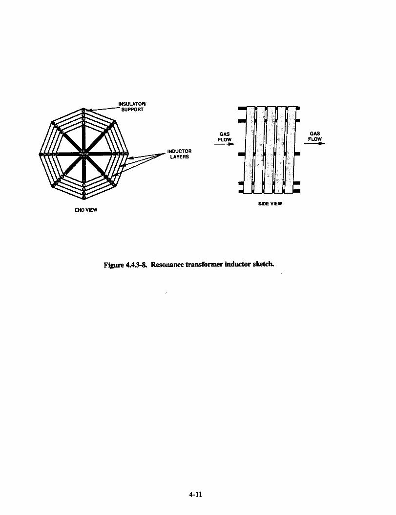
END VIEW
INSULATOR/
SUPPORT
INDUCTORLAYERS
GASFLOW
1
iii i!I_:_! •
_i_i! ! __'_i_I_i_i_'_Iiiii_ii
l_::!_!ilI
_ i !il___J•_DE VIEW
GASFLOW
Figure 4.4.3-8. Resonance transformer inductor sketch.
4-11
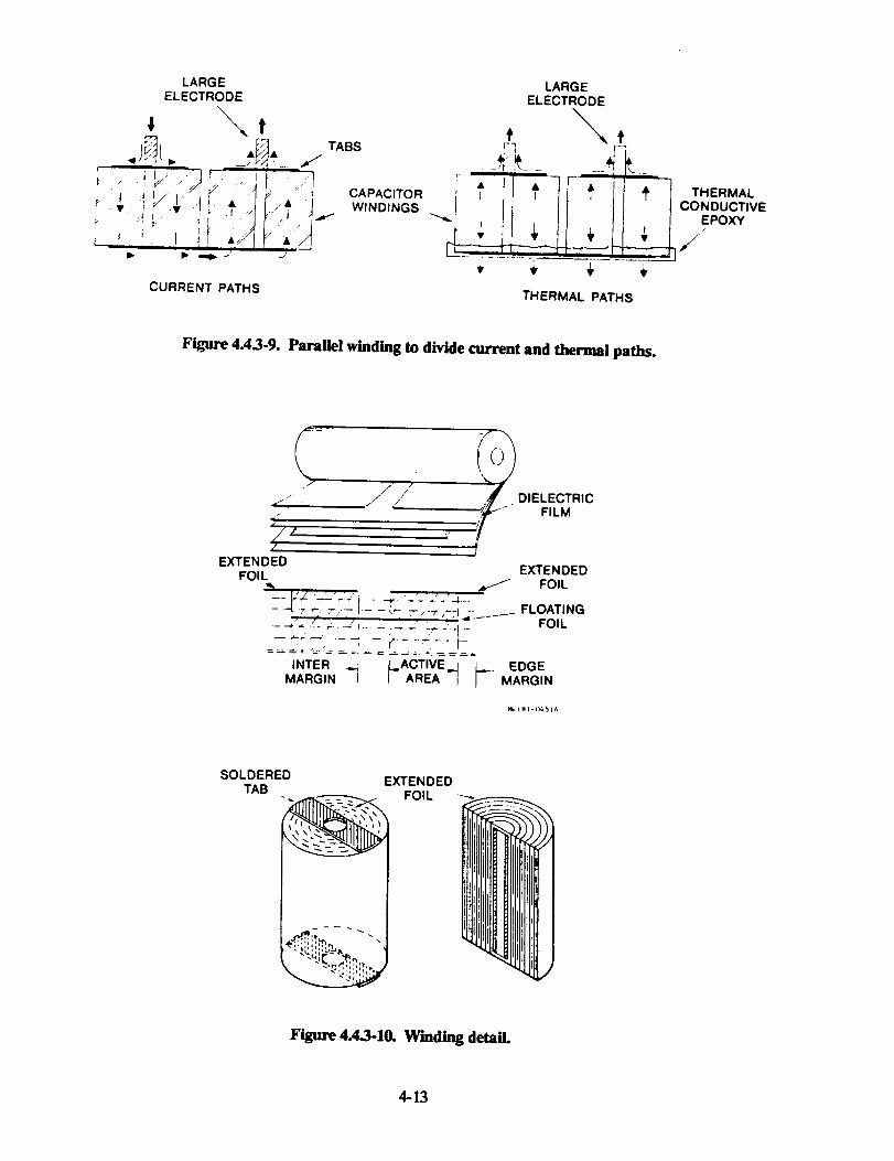
LARGEELECTRODE
• -7 "_ l
! i ,t '
CURRENT PATHS
CAPACITORWINDINGS
,f
_;7_
LARGEELECTRODE
",,,
, / gPOXY
THERMAL PATHS
Figure 4.4.3-9. Parallel winding to divide current and thermal paths.
.. // /:
q
_//'t .:
DIELECTRICFILM
EXTENDEDFOIL
_, / FOIL
-- 7 ,-" ,,' "["
.- -('*;/.';.--/t .... !.'- 3 -r : ,} ,- FOIL--i_ ...... -; -r .... --'t-
INTER _. _.ACTIVE,,_ _ EDGEMARGIN / AREA | / MARGIN
EXTENDED
Mt till-(_IA
SOLDERED EXTENDED
TAB "__ FOIL
,_',,.-_.:_r-_-_,,
Figure 4.43-10. Winding detail
4-13
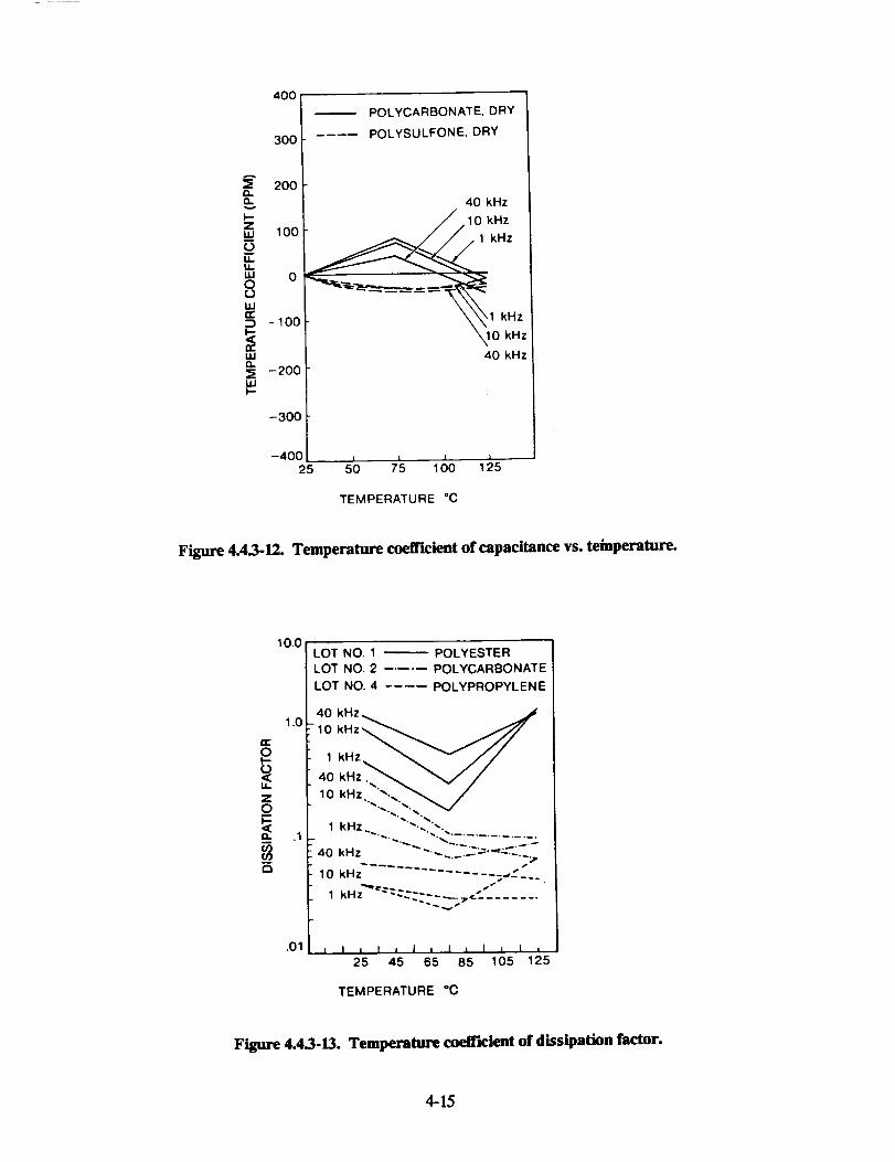
400
300
200
_ 100
oOOIJJn,-
-100LIJtt
-200wI-
-300
POLYCARBONATE, DRY
POLYSULFONE, DRY
-400 L l l A25 50 75 100 125
40 kHz
/10 kHz
/1 kHz
_10 k:_z
40 kHz
TEMPERATURE °C
Figure 4.4.3-]2. Temperature coel_icient of capacitance vs. tei-perature.
_rO
u.Z_o
Q.
C3
10.0
1.0
.01
LOT NO. 1 _ POLYESTER
LOT NO. 2 ..... POLYCARBONATE
LOT NO. 4 .... POLYPROPYLENE
40 kHz_ j¢
kHz _ "
40 kHz
lo kHz..'-.._ /
1 kHz ..'_
40 kHz ._ ........ _._._
10 kHz _
1 kHz'_C--___7_. _
, l , [ i | : I , I l I ,25 45 65 85 105 125
TEMPERATURE "C
Figure 4.43-13. Temperature coefficient of dissipation factor.
4-15
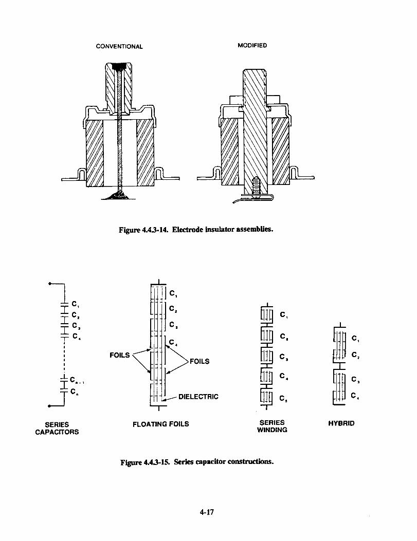
CONVENTIONAL MODIFIED
Figure 4.43-14. Electrode insulator assemblies.
C,C,
C=
C,
tc.
FOILS _ _ FOILS
_1 DIELECTRIC
C,
_c.
_c,
EI_c.C,
i l
C_
C=
C,
SERIESCAPACITORS
FLOATING FOILS SERIESWINDING
HYBRID
Figure 4.4.3-15. Series capacitor constructions.
4-17
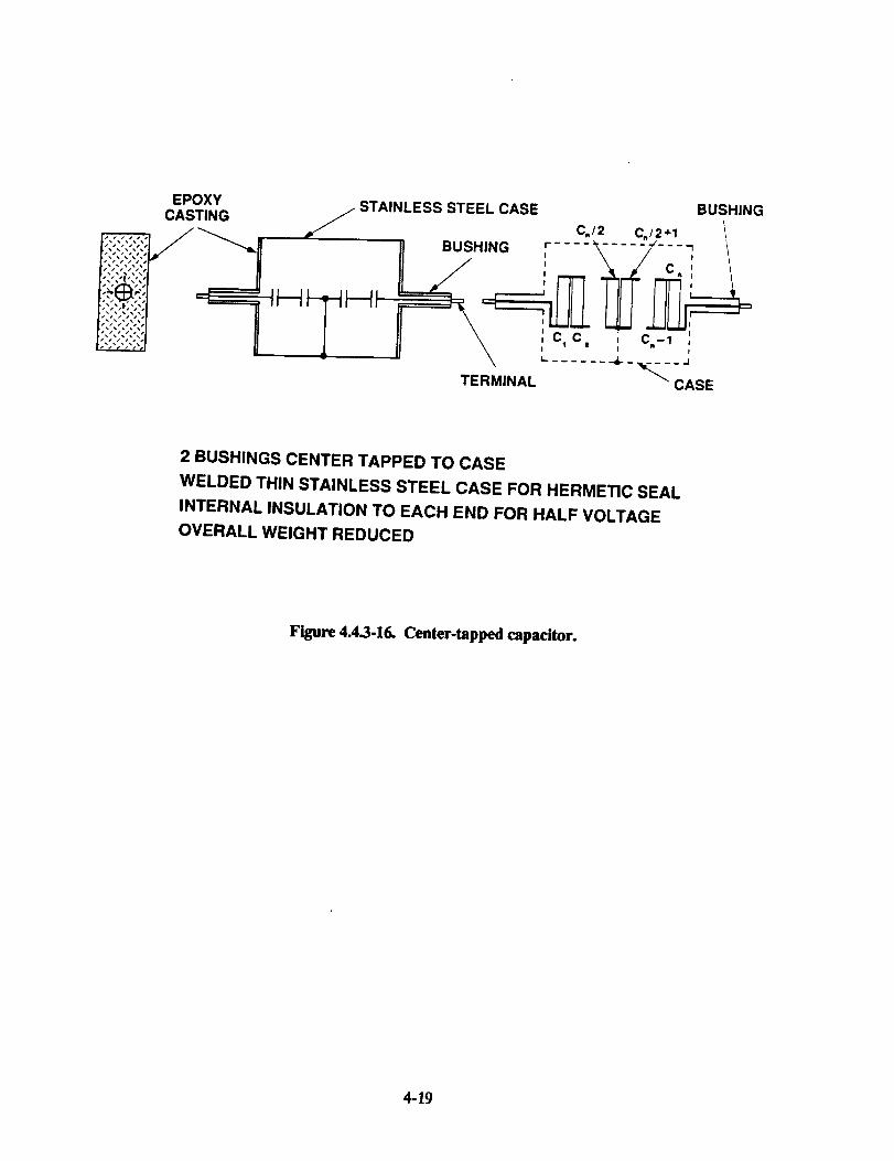
EPOXYCASTING
ll"s't'J'/',
,_s_,_,_,_:$/1t11,
STAINLESS STEEL CASE BUSHING
C,,/2 C,,/2+1 _
II BUSHING ,r .... \-- "--7/- - - _ /
II \ I C,-1
" \ _"...... _ - _ CASETERMINAL
2 BUSHINGS CENTER TAPPED TO CASE
WELDED THIN STAINLESS STEEL CASE FOR HERMETIC SEAL
INTERNAL INSULATION TO EACH END FOR HALF VOLTAGE
OVERALL WEIGHT REDUCED
Figure 4A.3-16. Center-tapped capacitor.
4-19
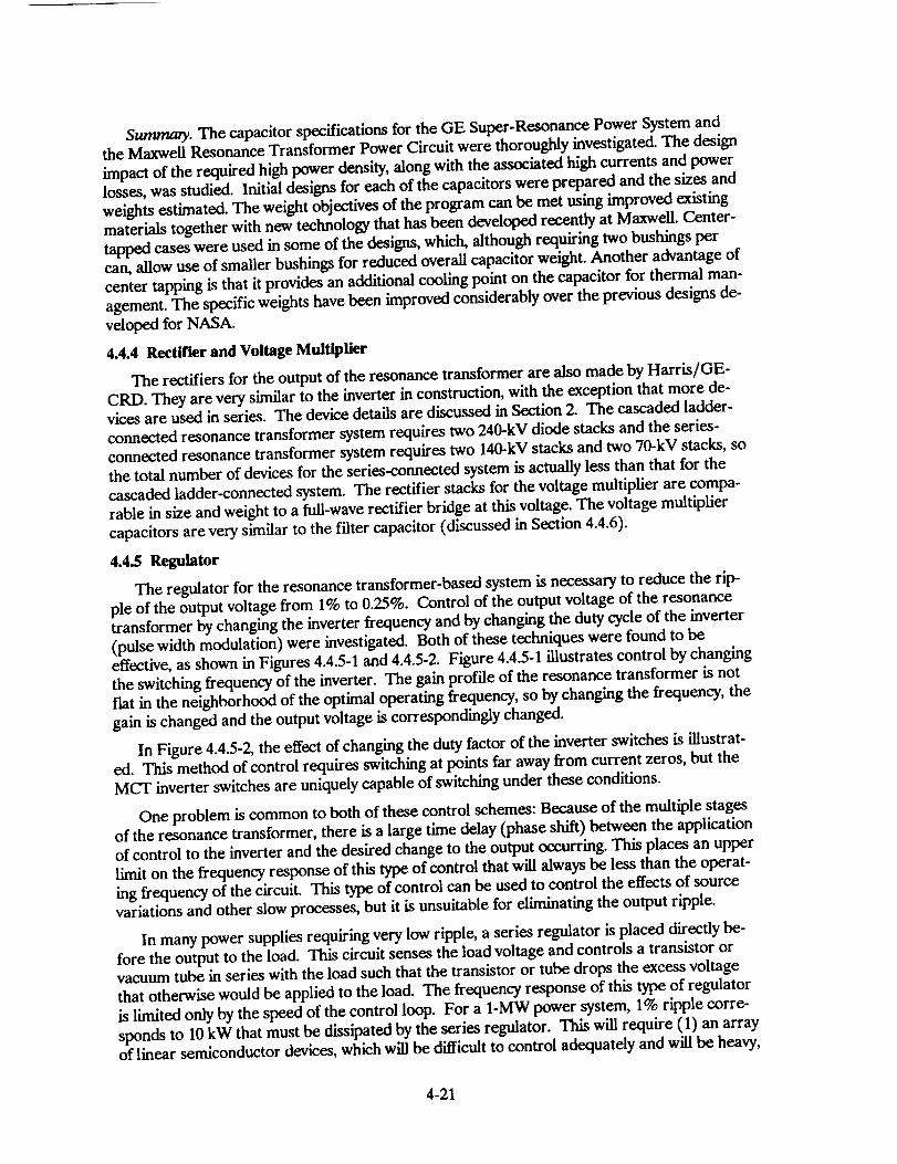
Summary. The capacitor specifications for the GE Super-Resonance Power System andthe Maxwell Resonance Transformer Power Circuit were thoroughly investigated. The design
impact of the required high power density, along with the associated high currents and power
losses, was studied. Initial designs for each of the capacitors were prepared and the sizes and
weights estimated. The weight objectives of the program can be met using improved existing
materials together with new technology that has been developed recently at Maxwell. Center-
tapped cases were used in some of the designs, which, although requiring two bushings percan, allow use of smaller bushings for reduced overall capacitor weight. Another advantage of
center tapping is that it provides an additional cxmling point on the capacitor for thermal man-agement. The specific weights have been improved considerably over the previous designs de-
veloped for NASA.
4.4.4 Rectifier and Voltage Multiplier
The rectifiers for the output of the resonance transformer are also made by Harris/GE-
CRD. They are very similar to the inverter in construction, with the exception that more de-vices are used in series. The device details are discussed in Section 2. The cascaded ladder-
connected resonance transformer system requires two 240-kV diode stacks and the series-
connected resonance transformer system requires two 140-kV stacks and two 70-kV stacks, so
the total number of devices for the series-connected system is actually less than that for thecascaded ladder-connected system. The rectifier stacks for the voltage multiplier are compa-
rable in size and weight to a full-wave rectifier bridge at this voltage. The voltage multiplier
capacitors are very similar to the filter capacitor (discussed in Section 4.4.6).
4.4.5 Regulator
The regulator for the resonance transformer-based system is necessary to reduce the rip-
ple of the output voltage from 1% to 0.25%. Control of the output voltage of the resonance
transformer by changing the inverter frequency and by changing the duty cycle of the inverter(pulse width modulation) were investigated. Both of these techniques were found to be
effective, as shown in Figures 4.4.5-1 and 4.4.5-2. Figure 4.4.5-1 illustrates control by changing
the switching frequency of the inverter. The gain profile of the resonance transformer is not
flat in the neighborhood of the optimal operating frequency, so by changing the frequency, the
gain is changed and the output voltage is correspondingly changed.
In Figure 4.4.5-2, the effect of changing the duty factor of the inverter switches is illustrat-
ed. This method of control requires switching at points far away from current zeros, but the
MCT inverter switches are uniquely capable of switching under these conditions.
One problem is common to both of these control schemes: Because of the multiple stages
of the resonance transformer, there is a large time delay (phase shift) between the application
of control to the inverter and the desired change to the output occurring. This places an upperlimit on the frequency response of this type of control that will always be less than the operat-
ing frequency of the circuit. This type of control can be used to control the effects of source
variations and other slow processes, but it is unsuitable for eliminating the output ripple.
In many power supplies requiring very low ripple, a series regulator is placed directly be-
fore the output to the load. This circuit senses the load voltage and controls a transistor or
vacuum tube in series with the load such that the transistor or tube drops the excess voltage
that otherwise would be applied to the load. The frequency response of this type of regulator
is limited only by the speed of the control loop. For a 1-MW power system, 1% ripple corre-
sponds to 10 kW that must be dissipated by the series regulator. This will require (1) an array
of linear semiconductor devices, which will be difficult to control adequately and will be heavy,
4-21
or (2)avacuumtube,whichwill requireanisolatedpowersupplyandcontrolelectronicsandwhich will also be heavy.
A third option is a regulation scheme developed by Maxwell (Figure 4.4.5-3). The regula-tor consists of a number of parallel combinations of FET switches and resistors in series with
the load. The switches place the resistors in series with the load and remove them to control
the load voltage. The minimum number of switch/resistor combinations required is deter°
mined by
n = (input ripple voltage)/(output ripple voltage)
where n is the number of switch/resistor combinations. The power dissipation per resistor is
determined by
PR = Pout * (input ripple voltage)/(Vout * n),
where PR is the power per resistor, Pout is the load power, Vout is the load voltage, and n is the
number of switch/resistor combinations.
The operation of this regulator is straightforward. There are two output voltage thresh-
olds for the switch control. These correspond to the minimum and maximum allowable load
voltage. Initially, all the switches are dosed. When the voltage across the load reaches the
upper threshold, one switch opens, placing a resistor in series with the load and lowering the
load voltage to the lower voltage threshold. As the load voltage continues to climb to theupper threshold, more switches are opened until the voltage fails to reach the upper threshold.
When the voltage tries to drop below the lower threshold, the switches close sequentially to
keep the load voltage within the proper range. This regulator has proven to be stable in com-puter simulations as long as the change in voltage produced by opening or closing a switch
does not exceed the difference of the upper and lower thresholds. In the case of a load fault,
the switches will all close to prevent damage to the regulator.
The frequency response of this regulator depends on the number of switch/resistor combi-nations and how fast they can be switched on and off. Since the number of switch/resistor
combinations depends upon the required regulation, a higher degree of regulation is achieved
at the expense of a reduced bandwidth. For a regulator with 10 switch/resistor combinations
(2 kV ripple _ 200 V ripple, for example), a bandwidth of 1 MHz should be poss_le toachieve.
For the two systems under discussion, the switches chosen are IRFP460 FETs. These
FETs are efficient, highly reliable, and can operate at greater than 1 MHz, which is necessaryfor effective regulation. The 20-n resistors will be made from 10 m of 16 AWG Nichrome
wire. The power dissipation in the N/chrome is 10 W/g, which should be a safe level in view
of the cooling available. The control voltage and electronics power will be picked off the out-
put voltage, and the entire regulator assembly will float at 100 kV.
4.4.6 Filter Inductor and Capacitor
The filter inductor is similar in construction to the resonance transformer inductors, pri-
marily for weight and cooling considerations as opposed to performance considerations. It is
the largest inductor at 15 mH, and is only required in the cascaded ladder-connected system.
The filter capacitor will have the same dielectric system and similar construction as the
resonance transformer capacitors (discussed in Section 4.4.3). The requirements for ac and
filter capacitors are different, but in this case the best dielectric system for these two applica-
tions was the polypropylene/MIPB combination.
4-23
4.4.7 Crowbar
The crowbar switch is required to limit the fault energy in case of a load fault to a few tens
of joules. It accomplishes this by sensing a load overcurrent and firing to divert the current
away from the load. The same sensing circuit will close the regulator to protect it, but thecrowbar switch will fire first to allow the regulator resistance to aid in diverting the fault cur-
rent to the crowbar switch. The crowbar circuit with trigger is shown in Figure 4.4.7-1. A
Hall probe senses an overcurrent, which changes the state of a fast comparator with a zenerdiode reference voltage. The output of the comparator drives a pulse transformer, which
triggers a KN22B krytron switch. This switch dumps a charged 1-_F capacitor into the pri-
mary of a pulse transformer. The secondary of that pulse transformer is tied to the triggerelectrode of the crowbar spark gap. When the crowbar spark gap fires, it will continue toconduct until the filter and the resonance transformer are discharged and the load is safe.
This very lightweight, rugged circuit has been used in a number of systems at Maxwell. The
crowbar designed for the present system will handle up to 1.5 kJ easily and can be upgraded if
necessary for higher fault energies.
4.4.8 Housing, Support, and Cooling Structures
The housing, support, and cooling structures for the system are closely interrelated, with
most parts functioning in one or more of the above capacities. The designs are driven by the
following major requirements:
- The system is cooled with He at 50 K
- The housing must be light in weight
- The housing must hold 3 arm of H 2 during system operation
The cooling requirements are determined primarily by the power dissipation of the reso-nance transformer inductors. The overall efficiency of the system is about 88%. Approxi-
mately 80% of these losses are in the inductors. TheH2 inlet temperature is assumed to be
50 K and the outlet temperature is 200 K. Based on a system efficiency of 88% and those in-
let and outlet temperatures, the estimated H2 inlet and outlet flow rates are 195 L/s
(412 R3/m) and 779 L/s (1651 ft3/m), respectively. The original design used an inlet temper-
ature of 25 K, but there was some concern that this was too close to the phase change temper-
ature to ensure predictable cooling and high-voltage insulation performance.
The housing is only required to hold pressure during 1000 seconds of operation, plus test-
ing. It is very difficult to make a container that will remain sealed for the required system life
of on the order of 10 years and hold pressure while remaining light in weight. Because the
only time the pressurization is required is during operation, and because the hydrogen is avail-
able during the alert period leading up to system operation, on-demand pressurization is pos-
s_le. This reduces the requirements for the housing. For example, pinholes caused by mi-crometeoroids are not an issue in a on-demand pressurized system. This means that the
housing can be a non-rigid structure that inflates on demand. The hydrogen inlet to this hous-
ing is a large-diameter tube to which all the components are mounted, forming the backbone
of the housing. The cooling plena connect the tube to the various cryocooled components and
provide support for the inductors, the inverter, and the diode stacks. This allows cooling hy-
drogen to flow directly to the individual inductors and semiconductor stacks. The exhaust hy-
drogen then pressurizes the housing. A relief valve maintains the pressure at 3 atm.
The capacitors and the regulator are also mounted to the central tube. A septum sepa-
rates the inductor volume from the capacitor volume. This, along with the small cross-
4-25
sectionalareaof the connections between the inductors and the capacitors, allows the capaci-
tors to remain at a much warmer operating temperature than the inductors. The overall size
of the housing is 7 ft long x 2 ft in diameter.
4.5 System Selection, Mass Effk:iency, and Layout
The masses for both the cascaded ladder-connected (CLC) resonance transformer-based
system and the symmetric series-connected (SSC) resonance transformer-based system havebeen calculated, based on careful design of the components and verification of those designs
by computer simulations, and are listed in Table 4.5-1. The overall efficiency of both of thesesystems is estimated at 87%; 66% of the losses are in the resonance transformer inductor,20% in the inverter, 5% in the regulator, 4% in the diodes, and the remainder in the other
components. The resonance transformer inductor losses were calculated at room temperatureand will be lower in the actual system due to the cooler temperatures.
Table 4.5-1
Mass Breakdown
Component CLC (kg) SSC (kg)
Input fuse 1.0 1.0
Input filter capacitor 2.0 2.0Inverter 8.0 8.0
Resonance transformer capacitors 20.8 20.8Resonance transformer inductors 12.8 16.0
Voltage multiplier capacitors - 12.6Diode stacks 4.0 3.3
Filter inductor 4.8 -
Filter capacitor 10.0 7.4Crowbar circuit 1.8 1.8
Regulator circuit 5.2 2.6
Cooling plena 4.3 3.3
Component supports 1.0 1.0
Envelope 4.0 4.0
Totals 79.7 83.8
The symmetric series-connected resonance transformer-based system has performance
characteristics that are superior to the cascaded ladder-connected resonance transformer-
based system (Section 4.4). As a result, the symmetric series-connected resonancetransformer-based system was chosen for the high-power, high-voltage, dc-dc converter. This
system will meet or exceed all the specifications for this converter. A conceptual layout of the
housing and the converter system together is shown in Figure 4.5-1.
4.6 Risk Areas and Risk Abatement
As with any new design, some risk is involved with this approach. Some typical system is-
sues for space-based systems are discussed in Section 4.3. This section discusses the risks in-herent to this system specifically and the plans to minimize these risks when the actual design
and construction of the prototype are undertaken.
4-27
4.6.1 Resonance Transformer-Based Systems
One of the risks associated with the use of a resonance transformer-based system is that
only a few systems of this type have been designed and only one has been constructed to date.However, the fact that a working model has been constructed demonstrates the validity of the
concept, and reduces this particular risk to that associated with making the components to the
required specifications. The small-scale testing of components (Section 4.4) indicates that the
components can indeed be designed to meet the requirements for this converter. This risk willbe further reduced by careful component design and further small scale testing in Phase 2 of
the program.
4.6.2 cryocooUng
The main risks associated with using cryogenic hydrogen gas to cool some of the com-
ponents are that (1) the capacitors cannot survive if they are cooled to the hydrogen tempera-
ture, (2) there may be materials problems with hydrogen cooling, and (3) loss of coolant can
quickly lead to component damage. The first risk is mitigated by housing the capacitors in a
separate volume from the rest of the components and by ensuring that the thermal conduction
through the electrical connections to the capacitors is minimized. The second risk is mini-mized by a careful selection of materials for the system and by plating the metals with anembrittlement-resistant material if necessary, as described in Section 4.3.5. The third risk is
alleviated by ensuring that the controls system shuts the power system down if coolant flow is
lost or if an overtemperature occurs.
4.6.3 Semiconductors in Space
The risks of the use of semiconductor devices in space have been a topic of concern in the
power community for a number of years. The degradation of semiconductor device perfor-mance over time when exposed to the ambient space environment has been documented.MCTs are new devices and have not been characterized as thoroughly as the older devices.The manufacturer of MCTs is confident that the devices can be made as hard as any other
semiconductor device. If this is not pdss_le, then other, more hardened devices such as FETs
or BJTs can be used for the switches in this system. The system performance and mass will
be adversely affected, but not to a large enough degree that the system is not viable withoutthe MCTs.
4.6.4 Regulator Scheme
The regulator scheme proposed promises to be a very lightweight subsystem, but it has
never been used in a power system. This means it has never demonstrated stability in a real
system. However, it has proven to be very stable in circuit simulations, and the components
used to make it are highly reliable. The stability of this system will also be demonstrated in asmall-scale demonstration in Phase 2.
4.7 System Scalability
The 1-MW system presented above is exceptionally light in weight and has a much higher
power density than that achievable with converters currently in use. One of the features of the
resonance transformer-based system is that the power density increases when the output
power is increased for a fixed input and output voltage. This is true for power levels up to at
least the hundreds of megawatts regime, which is the largest point design of a resonancetransformer-based system performed to date. To demonstrate this, a system with 10 MW out-
put power was investigated to determine the power density at this level. The results are tabu-lated in Table 4.7-1.
4-29
Section 5
CONCLUSIONS
The advanced power conversion system designs evaluated during Phase 1 of this program
represent an extension of dc-to-dc converter technology to well beyond the present state ofthe art. Different tradeoffs were necessarily invoked for the two subject designs. The present
study shows that both systems can in theory meet the stringent 0.1 kg/kW power density while
operating in the space environment.
The super-resonant approach developed by GE, presently being used in a product applica-tion to a power level of approximately 70 kW, has demonstrated a high level of reliability. The
present study extends this technology to the 1-MW power level and also includes a new, inno-vative control scheme that has the potential to further enhance the reliability of operation.
The resonance transformer approach developed at Maxwell avoids the use of a high-
voltage transformer through the use of a new circuit configuration employing components
with proven performance where possible. This use of mature components should make the
overall system very reliable.
Both system approaches will exhibit higher power density at higher power levels.
Table 5-1 compares the two systems in terms of mass, power dissipation, efficiency andenclosed volume.
Table 5-1
System Comparison
Converter Component
System Approach
Super-Resonant Resonance TransformerMass Loss Mass Loss
(kg) (W) (kg) (W)
Input fuse 1.0 10 1.0
Dc input filter capacitor 3.0 5 2.0Inverter 8.0 42400 8.0
Power circuit 44.0* 12236* 52.7
Dc output filter capacitor 14.0 60 7.4Dc output crowbar 2.0 0 1.8Control electronics 0.5 2.6
Cooling system 10.0 1000 3.3
Component support structure 4.5 1.0
Envelope enclosure (ft 3) 1.5 (10) 4.0 (22)
Total system 88.5 55711 83.8
System efficiency 94.4% 87.2%
5
5
40000
1014001
0
5000
146411
*Includes the resonant inductor and capacitor, transformer and high-voltage output rectifier
5-1

Section 6
PROPOSED FOLLOW-ON ACTIVITY
6.1 Program Phase 2
GE and Maxwell Laboratories propose to develop their specific approaches conducted as
parallel efforts. Both systems use an MCr-based inverter of nearly identical design. This
parallel approach uses the synergy developed between GE and Maxwell and permits thedevelopment of both systems at a cost that is much less than if they were to be developed sep-
arately. Harris Semiconductor will develop one MCT module type to be used with both sys-
tem approaches.
6.1.1 Phase 2A- 100-kW Proof-of-Principle Breadboard Development (One Year)
GE will develop one air-cooled, MCT-based, 100-kW super-resonant converter bread-
board using a 1-MW transformer, suitable for laboratory testing. A simple form of optimal
closed-loop control will be developed. Only one 1-MW transformer will be built for use withthe breadboard.
Maxwell will develop one air-cooled, MCT-based, 100-kW resonance-transformer convert-
er system and provide testing. A "bare-bones" closed-loop control will be provided.
For each system, the 100-kW proof-of-principle converter hardware shall comprise an op-
erating breadboard sufficient to obtain any necessary data in a laboratory environment.
Maxwell will be responsible for all capacitors, power supply, input fuse, resonance transform-
er, crowbar circuit, dummy load, and housing for both systems. GE will provide the inverter
and output rectifiers for both systems. No component-level testing will be performed. Maxwellwill perform all high-voltage system-level testing.
Gaseous hydrogen cooling, completion of optimal control (GE), and 1-MW breadboard
hardware development are proposed for the next phase.
6.1.2 Phase 2B- I-MW Proof-of-Principle Breadboard Development (One Year)
As with Phase 2A, GE and Maxwell Labs will continue to develop their specific ap-
proaches to be conducted as parallel efforts. Harris Semiconductor will develop one MCT
module type to be used with both system approaches.
GE will develop one air-cooled, MCT-based, 1-MW super-resonant converter breadboard
suitable for laboratory testing. A simple form of optimal dosed-loop control will be used. The
1-MW transformer developed for Phase ZA will be utilized with the 1-MW breadboard.
Maxwell will develop one air-cooled, MCT-based, 1-MW resonance-transformer convert-
er system and provide testing. A "bare-bones" closed-loop control will be provided.
For each system, the 1-MW hardware shall comprise an operating breadboard sufficient
to obtain any necessary data in a laboratory environment. Maxwell will be responsible for all
capacitors, power supply, input fuse, resonance transformer, crowbar circuit, dummy load,
and housing for both systems. GE will provide the inverter and output rectifiers for both sys-
tems. Maxwell will perform all high-voltage system-level testing.
Gaseous hydrogen cooling, completion of optimal control (GE), and 1-MW brassboard
hardware development are proposed for the next phase.
6-1
Aet_ttaal snO Report Documentation Page
I. Report No. I
NASA CR-187116
4, Title and Subtitle
2. Government Accession No. 3. Recipient's Catilog No.
5. Report Dme
High-Power Converters for Space Applications
7. Author(s)
J.N. Park, GE-CRD; Randy Cooper, Maxwell Laboratories
9. Performing Organization Nlme and Address
Prime contractor: GE Corporate Research and Development
P.O. Box 8, Schenectady, NY 12301
12. Sponsoring Agency Nm and Addreml
National Aeronautics and Space AdministrationLewis Research Center
Cleveland, OH 44135-3191
June 1991
6. Performing OrganizationCode
8. Performing Organization Report No.
90SRD008
10. Work Unit No.
506-41-3F
11. Contract or Grant No.
NAS3-25800
13. Type of Report and Period Covered
Contractor ReportFinal
14. Sponsoring Agency Code
15. Supplementary Notes
Project Manager: Ira T. Myers, Power Technology Division, NASA Lewis Research Center
Subcontractor: Maxwell Laboratories,
8888 Balboa Avenue, San Diego, CA 92123-1506
16. Abstract
Phase 1 was a concept definition effort to extend space-type dc/dc converter technology to tlmegawatt level with a weight of less than 0.1 kg/kW (220 lb/MW). Two system designs were evaluate
in Phase 1. Each design operates from a 5-kV stacked fuel cell source and provides a voltage step-up
100 kV at 10 A for charging capacitors (100 pps at a duty cycle of 17 min on, 73 min off). Both desig]use an MCT-based, full-bridge inverter, gaseous hydrogen cooling, and crowbar fault protection.
The GE-CRD system uses an advanced high-voltage transformer/rectifier filter in series with
resonant tank circuit, driven by an inverter operating at 20 to 50 kHz. Output voltage is controllt
through frequency and phase shift control. Fast transient response and stability is ensured via "optim
control." Super-resonant operation employing MCTs provides the advantages of lossless snubbing, r
turn-on switching loss, use of medium-speed diodes, and intrinsic current limiting under load-fau
conditions. Estimated weight of the GE-CRD system is 88.5 kg (1.5 ft3). Efficiency is 94.4% and tot
system loss is 55.711 kW operating at 1 MW load power.
The Maxwell system is based on a resonance transformer approach using a cascade of five L
resonant sections at 100 kHz. The 5-kV bus is converted to a square wave, stepped-up to a 100-kV sin
wave by the LC sections, rectified, and filtered. Output voltage is controlled with a special seric
regulator circuit. Estimated weight of the Maxwell system is 83.8 kg (4.0 ft3). Efficiency is 87.2% antotal system loss is 146.411 kW operating at 1 MW load power.
17. Key Words (Suggested by Author(i))
light weight; high-power conveners;high-voltage, high-frequency converters
18. Dist_ Statement
Unclassified - Unlimited
Subject Category 33
19. Security Classif. (of this reporl) 20. Security Clusif. (of this plge) 21. No of pages
Unclassified Unclassified 139
N_A VO_= _sz_ oct u "For sale by the National Technical Information Service, Springfield, Virginia 22161
Price °
A07