Embed Size (px)
Citation preview
July 2010 Doc ID 15257 Rev 4 1/33
33
STCF05
High power white LED driver with I²C interface
Features■ Boost DC-DC converter with synchronous
rectification
■ Drives 2 power white LEDs in series with a current up to 400 mA
■ Input voltage range 2.5 V to 5.5 V
■ Needs 3 external components only
■ Output current control
■ 1.8 MHz fixed frequency PWM control
■ Peak inductor current limited to 3 A
■ Full I²C control
■ Operational modes:– Standby mode– Standby mode with NTC– Flash mode: up to 400 mA– Torch mode: up to 120 mA
■ Soft and hard triggering of flash
■ Flash and Torch dimming in 15 exponential steps
■ Dimmable red LED indicator auxiliary output
■ Internally or externally timed flash operation
■ Digitally programmable safety time-out in flash mode
■ LED overtemperature detection and protection with external NTC resistor
■ Open and shorted LED failure detection and protection
■ Chip overtemperature detection and protection
■ Less than 1 µA standby current
■ Package 3 x 3 mm TFBGA25
Applications■ Cell phones and smartphones
■ Camera flashes/strobe
■ PDAs and digital still cameras
DescriptionThe STCF05 is a high efficiency power supply solution to drive multiple flash LEDs in camera phones, PDAs and other hand-held devices. The synchronous boost topology with output current control guarantees the proper LED current over all possible conditions of battery level and LED forward voltage. All the functions of the device are controlled through the I²C bus that allows to reduce logic pins on the package and to save PCB traces on the board. Hard and soft-triggering of the flash are both supported. The device includes many functions to protect the chip and the power LEDs. These comprehend a soft-start control, chip over temperature detection and protection, open and shorted LEDs detection and protection. In addition, a digital programmable time-out function protects the LEDs in case of wrong command from microprocessor. See description (continued).
TFBGA25 (3 x 3 mm)
Table 1. Device summary
Order code Package Packaging
STCF05TBR TFBGA25 (3 x 3 mm) 3000 parts per reel
www.st.com

Contents STCF05
2/33 Doc ID 15257 Rev 4
Contents
1 Description (continued) . . . . . . . . . . . . . . . . . . . . . . . . . . . . . . . . . . . . . . 5
2 Diagram . . . . . . . . . . . . . . . . . . . . . . . . . . . . . . . . . . . . . . . . . . . . . . . . . . . 6
3 Pin configuration . . . . . . . . . . . . . . . . . . . . . . . . . . . . . . . . . . . . . . . . . . . 7
4 Maximum ratings . . . . . . . . . . . . . . . . . . . . . . . . . . . . . . . . . . . . . . . . . . . . 8
5 Application . . . . . . . . . . . . . . . . . . . . . . . . . . . . . . . . . . . . . . . . . . . . . . . . . 9
6 Electrical characteristics . . . . . . . . . . . . . . . . . . . . . . . . . . . . . . . . . . . . 10
7 Detailed description . . . . . . . . . . . . . . . . . . . . . . . . . . . . . . . . . . . . . . . . 12
7.1 Introduction . . . . . . . . . . . . . . . . . . . . . . . . . . . . . . . . . . . . . . . . . . . . . . . 12
7.2 Boost converter . . . . . . . . . . . . . . . . . . . . . . . . . . . . . . . . . . . . . . . . . . . . 12
7.3 Logic pin description . . . . . . . . . . . . . . . . . . . . . . . . . . . . . . . . . . . . . . . . 12
7.3.1 SCL, SDA pins . . . . . . . . . . . . . . . . . . . . . . . . . . . . . . . . . . . . . . . . . . . . 12
7.3.2 TRIG pin . . . . . . . . . . . . . . . . . . . . . . . . . . . . . . . . . . . . . . . . . . . . . . . . 12
7.3.3 ATN pin . . . . . . . . . . . . . . . . . . . . . . . . . . . . . . . . . . . . . . . . . . . . . . . . . 12
7.3.4 ADD pin . . . . . . . . . . . . . . . . . . . . . . . . . . . . . . . . . . . . . . . . . . . . . . . . . 13
7.3.5 TMSK pin . . . . . . . . . . . . . . . . . . . . . . . . . . . . . . . . . . . . . . . . . . . . . . . . 13
8 I²C bus interface . . . . . . . . . . . . . . . . . . . . . . . . . . . . . . . . . . . . . . . . . . . 14
8.1 Data validity . . . . . . . . . . . . . . . . . . . . . . . . . . . . . . . . . . . . . . . . . . . . . . . 14
8.2 Start and stop conditions . . . . . . . . . . . . . . . . . . . . . . . . . . . . . . . . . . . . . 14
8.3 Byte format . . . . . . . . . . . . . . . . . . . . . . . . . . . . . . . . . . . . . . . . . . . . . . . . 15
8.4 Acknowledge . . . . . . . . . . . . . . . . . . . . . . . . . . . . . . . . . . . . . . . . . . . . . . 15
8.5 Interface protocol . . . . . . . . . . . . . . . . . . . . . . . . . . . . . . . . . . . . . . . . . . . 16
8.6 Writing to a single register . . . . . . . . . . . . . . . . . . . . . . . . . . . . . . . . . . . . 16
8.7 Writing to multiple registers with incremental addressing . . . . . . . . . . . . 17
8.8 Reading from a single register . . . . . . . . . . . . . . . . . . . . . . . . . . . . . . . . . 17
8.9 Reading from multiple registers with incremental addressing . . . . . . . . . 18
9 Registers description . . . . . . . . . . . . . . . . . . . . . . . . . . . . . . . . . . . . . . . 20

STCF05 Contents
Doc ID 15257 Rev 4 3/33
9.1 PWR_ON . . . . . . . . . . . . . . . . . . . . . . . . . . . . . . . . . . . . . . . . . . . . . . . . . 20
9.2 TRIG_EN . . . . . . . . . . . . . . . . . . . . . . . . . . . . . . . . . . . . . . . . . . . . . . . . . 20
9.3 TCH_ON . . . . . . . . . . . . . . . . . . . . . . . . . . . . . . . . . . . . . . . . . . . . . . . . . . 20
9.4 NTC_ON . . . . . . . . . . . . . . . . . . . . . . . . . . . . . . . . . . . . . . . . . . . . . . . . . . 20
9.5 FTIM_0~3 . . . . . . . . . . . . . . . . . . . . . . . . . . . . . . . . . . . . . . . . . . . . . . . . . 20
9.6 TDIM_0~2 . . . . . . . . . . . . . . . . . . . . . . . . . . . . . . . . . . . . . . . . . . . . . . . . 20
9.7 FDIM_0~2 . . . . . . . . . . . . . . . . . . . . . . . . . . . . . . . . . . . . . . . . . . . . . . . . 21
9.8 LDIM . . . . . . . . . . . . . . . . . . . . . . . . . . . . . . . . . . . . . . . . . . . . . . . . . . . . . 21
9.9 AUXI_0~3 . . . . . . . . . . . . . . . . . . . . . . . . . . . . . . . . . . . . . . . . . . . . . . . . . 21
9.10 AUXT_0~3 . . . . . . . . . . . . . . . . . . . . . . . . . . . . . . . . . . . . . . . . . . . . . . . . 22
9.11 LED_S . . . . . . . . . . . . . . . . . . . . . . . . . . . . . . . . . . . . . . . . . . . . . . . . . . . 22
9.12 F_RUN . . . . . . . . . . . . . . . . . . . . . . . . . . . . . . . . . . . . . . . . . . . . . . . . . . . 22
9.13 LED_O . . . . . . . . . . . . . . . . . . . . . . . . . . . . . . . . . . . . . . . . . . . . . . . . . . . 23
9.14 NTC_W . . . . . . . . . . . . . . . . . . . . . . . . . . . . . . . . . . . . . . . . . . . . . . . . . . . 23
9.15 NTC_H . . . . . . . . . . . . . . . . . . . . . . . . . . . . . . . . . . . . . . . . . . . . . . . . . . . 23
9.16 OT_F . . . . . . . . . . . . . . . . . . . . . . . . . . . . . . . . . . . . . . . . . . . . . . . . . . . . 23
9.17 OC_F . . . . . . . . . . . . . . . . . . . . . . . . . . . . . . . . . . . . . . . . . . . . . . . . . . . . 23
9.18 VOUTOK_N . . . . . . . . . . . . . . . . . . . . . . . . . . . . . . . . . . . . . . . . . . . . . . . 23
10 Detailed description . . . . . . . . . . . . . . . . . . . . . . . . . . . . . . . . . . . . . . . . 25
10.1 Power ON reset . . . . . . . . . . . . . . . . . . . . . . . . . . . . . . . . . . . . . . . . . . . . 25
10.2 Shutdown, shutdown with NTC . . . . . . . . . . . . . . . . . . . . . . . . . . . . . . . . 25
10.3 Ready mode . . . . . . . . . . . . . . . . . . . . . . . . . . . . . . . . . . . . . . . . . . . . . . . 25
10.4 Single or multiple flash using external (microprocessor) temporization . . 25
10.5 External (microprocessor) temporization using TRIG_EN bit . . . . . . . . . 26
10.6 Single flash using internal temporization . . . . . . . . . . . . . . . . . . . . . . . . . 26
10.7 Multiple flash using internal temporization . . . . . . . . . . . . . . . . . . . . . . . . 26
11 Typical performance characteristics . . . . . . . . . . . . . . . . . . . . . . . . . . . 27
12 Package mechanical data . . . . . . . . . . . . . . . . . . . . . . . . . . . . . . . . . . . . 28
13 Revision history . . . . . . . . . . . . . . . . . . . . . . . . . . . . . . . . . . . . . . . . . . . 32

List of tables STCF05
4/33 Doc ID 15257 Rev 4
List of tables
Table 1. Device summary . . . . . . . . . . . . . . . . . . . . . . . . . . . . . . . . . . . . . . . . . . . . . . . . . . . . . . . . . . 1Table 2. Pin description . . . . . . . . . . . . . . . . . . . . . . . . . . . . . . . . . . . . . . . . . . . . . . . . . . . . . . . . . . . 8Table 3. Absolute maximum ratings . . . . . . . . . . . . . . . . . . . . . . . . . . . . . . . . . . . . . . . . . . . . . . . . . . 9Table 4. Thermal data. . . . . . . . . . . . . . . . . . . . . . . . . . . . . . . . . . . . . . . . . . . . . . . . . . . . . . . . . . . . . 9Table 5. List of external components . . . . . . . . . . . . . . . . . . . . . . . . . . . . . . . . . . . . . . . . . . . . . . . . 10Table 6. Electrical characteristics . . . . . . . . . . . . . . . . . . . . . . . . . . . . . . . . . . . . . . . . . . . . . . . . . . . 11Table 7. Address table . . . . . . . . . . . . . . . . . . . . . . . . . . . . . . . . . . . . . . . . . . . . . . . . . . . . . . . . . . . 14Table 8. Interface protocol . . . . . . . . . . . . . . . . . . . . . . . . . . . . . . . . . . . . . . . . . . . . . . . . . . . . . . . . 17Table 9. I²C register mapping read function . . . . . . . . . . . . . . . . . . . . . . . . . . . . . . . . . . . . . . . . . . . 20Table 10. Command register . . . . . . . . . . . . . . . . . . . . . . . . . . . . . . . . . . . . . . . . . . . . . . . . . . . . . . . 20Table 11. Dimming register. . . . . . . . . . . . . . . . . . . . . . . . . . . . . . . . . . . . . . . . . . . . . . . . . . . . . . . . . 20Table 12. Auxiliary register . . . . . . . . . . . . . . . . . . . . . . . . . . . . . . . . . . . . . . . . . . . . . . . . . . . . . . . . . 22Table 13. Auxiliary LED dimming table . . . . . . . . . . . . . . . . . . . . . . . . . . . . . . . . . . . . . . . . . . . . . . . 23Table 14. Torch mode and flash mode dimming registers settings . . . . . . . . . . . . . . . . . . . . . . . . . . 23Table 15. Status register. . . . . . . . . . . . . . . . . . . . . . . . . . . . . . . . . . . . . . . . . . . . . . . . . . . . . . . . . . . 23Table 16. Status register details . . . . . . . . . . . . . . . . . . . . . . . . . . . . . . . . . . . . . . . . . . . . . . . . . . . . . 25Table 17. Document revision history . . . . . . . . . . . . . . . . . . . . . . . . . . . . . . . . . . . . . . . . . . . . . . . . . 32

STCF05 List of figures
Doc ID 15257 Rev 4 5/33
List of figures
Figure 1. Block diagram . . . . . . . . . . . . . . . . . . . . . . . . . . . . . . . . . . . . . . . . . . . . . . . . . . . . . . . . . . . . 7Figure 2. Pin connections (top view) . . . . . . . . . . . . . . . . . . . . . . . . . . . . . . . . . . . . . . . . . . . . . . . . . . 8Figure 3. Application schematic . . . . . . . . . . . . . . . . . . . . . . . . . . . . . . . . . . . . . . . . . . . . . . . . . . . . . 10Figure 4. Data validity on the I²C bus. . . . . . . . . . . . . . . . . . . . . . . . . . . . . . . . . . . . . . . . . . . . . . . . . 15Figure 5. Timing diagram on I²C bus . . . . . . . . . . . . . . . . . . . . . . . . . . . . . . . . . . . . . . . . . . . . . . . . . 16Figure 6. Bit transfer . . . . . . . . . . . . . . . . . . . . . . . . . . . . . . . . . . . . . . . . . . . . . . . . . . . . . . . . . . . . . 16Figure 7. Acknowledge on I²C bus. . . . . . . . . . . . . . . . . . . . . . . . . . . . . . . . . . . . . . . . . . . . . . . . . . . 17Figure 8. Writing to a single register . . . . . . . . . . . . . . . . . . . . . . . . . . . . . . . . . . . . . . . . . . . . . . . . . 18Figure 9. Writing to multiple register with incremental addressing. . . . . . . . . . . . . . . . . . . . . . . . . . . 18Figure 10. Reading from a single register . . . . . . . . . . . . . . . . . . . . . . . . . . . . . . . . . . . . . . . . . . . . . . 19Figure 11. Reading from multiple registers . . . . . . . . . . . . . . . . . . . . . . . . . . . . . . . . . . . . . . . . . . . . . 19Figure 12. Current intensity vs. dimming value . . . . . . . . . . . . . . . . . . . . . . . . . . . . . . . . . . . . . . . . . . 22Figure 13. VOUTOK_N behavior . . . . . . . . . . . . . . . . . . . . . . . . . . . . . . . . . . . . . . . . . . . . . . . . . . . . . 25Figure 14. Efficiency in flash mode . . . . . . . . . . . . . . . . . . . . . . . . . . . . . . . . . . . . . . . . . . . . . . . . . . . 28Figure 15. Efficiency in torch mode . . . . . . . . . . . . . . . . . . . . . . . . . . . . . . . . . . . . . . . . . . . . . . . . . . . 28Figure 16. ILED vs. VBAT at different temp.. . . . . . . . . . . . . . . . . . . . . . . . . . . . . . . . . . . . . . . . . . . . . . 28Figure 17. ILED vs. VOUT . . . . . . . . . . . . . . . . . . . . . . . . . . . . . . . . . . . . . . . . . . . . . . . . . . . . . . . . . . . 28Figure 18. Input current vs. input voltage. . . . . . . . . . . . . . . . . . . . . . . . . . . . . . . . . . . . . . . . . . . . . . . 28Figure 19. Quiescent current in ready mode . . . . . . . . . . . . . . . . . . . . . . . . . . . . . . . . . . . . . . . . . . . . 28
Description (continued) STCF05
6/33 Doc ID 15257 Rev 4
1 Description (continued)
An optional external NTC is supported to protect the LEDs against over heating. In mobile phone application it is possible to reduce immediately the flash LEDs current during the signal transmission using the TMSK pin. This saves battery life and gives more priority to supply RF transmission instead of flash function.
It is possible to separately program the current intensity in flash and torch mode using exponential steps by I²C. In case of insufficient power from the battery a warning is generated. An auxiliary output can control an optional red LED to be used as a recording indicator.
The device is packaged in BGA 3 x 3 mm with 1 mm height.

STCF05 Diagram
Doc ID 15257 Rev 4 7/33
2 Diagram
Figure 1. Block diagram

Pin configuration STCF05
8/33 Doc ID 15257 Rev 4
3 Pin configuration
Figure 2. Pin connections (top view)
1 2 3 4 5
A VOUT LED LED ATN TRIG
B VOUT ADD SDA SCL TMSK
C PGND PGND PGND PGND AUXL
D VLX VLX PGND VBAT NTC
E VLX VLX PGND AGND RX
Table 2. Pin description
Ball n° Symbol Description
E1, D1, D2, E2 VLX Inductor connection
E5 RX Rx resistor connection
A1, B1 VOUT Output voltage
D5 NTC NTC resistor connection
C5 AUXL Auxiliary red LED connection
B4 SCL I²C clock signal
A5 TRIG Flash trigger input
E4 AGND Signal ground
B2 ADD I²C address selection
A2, A3 LED Diode cathode connection
A4 ATN Attention (open drain output, active LOW)
D4 VBAT Supply voltage
B3 SDA I²C data
B5 TMSK T-mask
C1, C2, C3, C4, D3, E3 PGND Power ground + die back connection

STCF05 Maximum ratings
Doc ID 15257 Rev 4 9/33
4 Maximum ratings
Note: Absolute maximum ratings are those values beyond which damage to the device may occur. Functional operation under these condition is not implied.
Table 3. Absolute maximum ratings
Symbol Parameter Value Unit
VBAT Signal supply voltage -0.3 to 6 V
VLX Inductor connection –0.3 to VO+0.3 V
OUT Output voltage -0.3 to 12 V
AUXL Auxiliary LED –0.3 to VBAT+0.3 V
LED LEDs connection –0.3 to VBAT+0.3 V
SCL, SDA, TRIG, ATN, ADD TMSK
Logic pin -0.3 to VBAT+0.3 V
RX Connection for reference resistor -0.3 to 3 V
NTC Connection for LED temperature sensing -0.3 to 3 V
ESD Human body model ± 2 kV
PTOT Continuous power dissipation (at TA = 70 °C) (1)
1. Power dissipation is dependent on PCB. The recommended PCB design is included in the application note.
800 mW
TOP Operating ambient temperature range -40 to 85 °C
TJ Junction temperature -40 to 150 °C
TSTG Storage temperature range -65 to 150 °C
Table 4. Thermal data
Symbol Parameter Value Unit
RthJA Thermal resistance junction-ambient (1) 56 °C/W
1. Using 1 inch2 of PCB area at 4-layers board.

Application STCF05
10/33 Doc ID 15257 Rev 4
5 Application
**: Connect to VI, or GND or SDA or SCL to choose one of the 4 different I²C slave addresses.
***: Optional components to support auxiliary functions. Vref = 1.8 V.
Note: Above listed components refer to typical application. Operation of the STCF05 is not limited to the choice of these external components.
Figure 3. Application schematic
Table 5. List of external components
Component Manufacturer Part number Value Size
CI TDK C1608X5R0J106M 10 µF 0603
CO TDK C1608X5R1A105M 1 µF 0603
L TDKVLF4014A-1R0N2R2 (1) 1 µH 3.7 x 3.5 x 1.2 [mm]
VLS252012T-1R0N1R7 (2) 1 µH 2.5 x 2 x 1.2 [mm]
NTC Murata NCP21WF104J03RA 100 kΩ 0805
RX RΩ MCR01MZPJ15K 15 kΩ 0402
LED Luxeon LED 2 x LXCL-PWF1 0805
1. Inductor type is recommended for high efficiency operation 85 % typ. at 400 mA output current.
2. This inductor type is recommended for the minimum app. area with typ. efficiency of the operation 77 % at 400 mA output current
STCF05 Electrical characteristics
Doc ID 15257 Rev 4 11/33
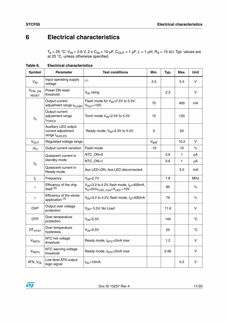
6 Electrical characteristics
TA = 25 °C, VIN = 3.6 V, 2 x CIN = 10 µF, COUT = 1 µF, L = 1 µH, RX = 15 kΩ. Typ. values are at 25 °C, unless otherwise specified.
Table 6. Electrical characteristics
Symbol Parameter Test conditions Min. Typ. Max. Unit
VINInput operating supply voltage
(1) 2.5 5.5 V
VPW_ON
RESET
Power ON reset threshold
VIN rising 2.3 V
IO
Output current adjustment range IFLASH
Flash mode for VIN=2.5V to 5.5V; VOUT=10V;
75 400 mA
Output current adjustment range ITORCH
Torch mode VIN=2.5V to 5.5V 15 120
Auxiliary LED output current adjustment range IAUXLED
Ready mode, VIN=3.3V to 5.5V 0 20
VOUT Regulated voltage range VBAT 10.2 V
ΔIO Output current variation Flash mode -10 10 %
IQ
Quiescent current in standby mode
NTC_ON=0 0.6 1 µA
NTC_ON=1 0.6 1 µA
Quiescent current in Ready-mode
Aux LED=ON, Aux LED disconnected 5.5 mA
fs Frequency VIN=2.7V 1.8 MHz
ν Efficiency of the chip itself (2)
VIN=3.2 to 4.2V, flash mode, IO=400mA, VO=2xVFLED_max+VLED =10V
85 %
νEfficiency of the whole application (3) VIN=3.2 to 4.2V, flash mode, IO=400mA 79 %
OVPOutput over voltage protection
VIN= 5.5V, No Load 11.6 V
OTPOver temperature protection
VIN=5.5V 140 °C
OTHYSTOver temperature hysteresis
VIN=5.5V 20 °C
VREF5NTC hot voltage threshold
Ready mode, INTC=2mA max 1.2 V
VREF4NTC warning voltage threshold
Ready mode, INTC=2mA max 0.56 V
ATN_VOL Low level ATN output logic signal
IOL=10mA 0.2 V

Electrical characteristics STCF05
12/33 Doc ID 15257 Rev 4
Symbol Parameter Test conditions Min. Typ. Max. Unit
IOZOutput logic leakage current ATN
VATN =3.3V 1 mA
VIL Low and high level input logic signals on SCL, SDA, TRIG, TEST
VIN=2.7V to 5.5V0 0.4 V
VIH 1.4 VI
TONLED current rise time ILED=0 to ILED=max
3 ms
1. Typical value, not production test.
2. Calculated as (VOUT*ILED)/(VIN*IIN)
3. Calculated as (VLED*ILED)/(VIN*IIN)
Table 6. Electrical characteristics (continued)
STCF05 Detailed description
Doc ID 15257 Rev 4 13/33
7 Detailed description
7.1 IntroductionThe STCF05 is a synchronous boost converter, dedicated to power and control the current of power white LEDs in a camera cell phones. The device operates at a typical constant switching frequency of 1.8 MHz. It steps an input voltage ranging from 2.5 V to 5.5 V up to 10.2 V. I²C bus controls device operation and diagnostic. Torch current is adjustable from 15 mA to 120 mA; flash current is adjustable up to 400 mA; aux LED current can be adjusted from 0 to 20 mA. The device uses an external NTC to sense the temperature of the white LEDs. These NTC functions may not be needed in all applications, and in those cases the relevant external components can be omitted.
7.2 Boost converterThe STCF05 contains the 3-loop system of the PWM controller regulation and soft-start function. When the output voltage is lower than input voltage, the STCF05 is charging output by the internal current source with 120 mA typ. When the output voltage is higher than battery, the STCF05 automatically enable the boost converter with 3-loop regulation system. First loop is controlling the output current according the setting of the dimming register, second loop is regulating the output voltage to the stable value and third loop is regulating the voltage drop on the LED current source to reach high efficiency of the operation. (see Figure 1: Block diagram).
7.3 Logic pin description
7.3.1 SCL, SDA pins
These are the standard clock and data pins as defined in the I²C bus specification. External pull-up is required according to I²C bus specifications.
7.3.2 TRIG pin
This input pin is internally and-ed with the TRIG_EN bit to generate the internal signal that activates the flash operation. This gives to the user the possibility to accurately control the flash duration using a dedicated pin, avoiding the I²C bus latencies (hard-triggering). No internal pull-up nor pull-down is provided.
7.3.3 ATN pin
This output pin (open-drain, active LOW) is provided to better manage the information transfer from the STCF05 to the microprocessor. Because of the limitations of a single master I²C bus configuration, the microprocessor should regularly poll the STCF05 to verify if certain operations have been completed, or to check diagnostic information. Alternatively, the microprocessor can use the ATN pin to be advised that new data are available in the STAT_REG, thus avoiding continuous polling. The information can be read in the STAT_REG by a read operation via I²C that, besides, automatically resets the ATN pin. The STAT_REG bits affecting the ATN pin status are mapped in Table 15. No internal pull-up is provided.

Detailed description STCF05
14/33 Doc ID 15257 Rev 4
7.3.4 ADD pin
With this pin it is possible to select one of the 4 possible I²C slave addresses. Neither internal pull-up nor pull-down is provided. The pin has to be connected to either GND, VI, SCL or SDA to select the desired I²C slave address (see Table 7)
7.3.5 TMSK pin
This pin can be used to implement the TX masking function. This function has effect for flash current settings higher than 100 mA (bit FDIM_3=1) only. Under this condition, when this pin is pulled high by the microprocessor, the current flowing in the LED is forced at 100 mA typ. Neither internal pull-up nor pull-down is provided. This pin must be externally wired to GND if TX masking function is not used.
Table 7. Address table
ADD pin A7 A6 A5 A4 A3 A2 A1 A0
GND 0 1 1 0 0 0 0 R/W
VBAT 0 1 1 0 0 0 1 R/W
SDA 0 1 1 0 0 1 0 R/W
SCL 0 1 1 0 0 1 1 R/W

STCF05 I²C bus interface
Doc ID 15257 Rev 4 15/33
8 I²C bus interface
Data transmission from the main microprocessor to STCF05 and vice versa takes place through the 2 I²C bus interface wires, consisting of the two lines SDA and SCL (pull-up resistors to a positive supply voltage must be externally connected).
8.1 Data validityAs shown in Figure 4, the data on the SDA line must be stable during the high period of the clock. The HIGH and LOW state of the data line can only change when the clock signal on the SCL line is LOW.
8.2 Start and stop conditionsBoth DATA and CLOCK lines remain HIGH when the bus is not busy. As shown in Figure 5 a start condition is a HIGH to LOW transition of the SDA line while SCL is HIGH. The stop condition is a LOW to HIGH transition of the SDA line while SCL is HIGH. A STOP condition must be sent before each START condition.
Figure 4. Data validity on the I²C bus

I²C bus interface STCF05
16/33 Doc ID 15257 Rev 4
8.3 Byte formatEvery byte transferred to the SDA line must contain 8 bits. Each byte must be followed by an acknowledge bit. The MSB is transferred first. One data bit is transferred during each clock pulse. The data on the SDA line must remain stable during the HIGH period of the clock pulse. Any change in the SDA line at this time will be interpreted as a control signal.
8.4 AcknowledgeThe master (microprocessor) puts a resistive HIGH level on the SDA line during the acknowledge clock pulse (see Figure 7). The peripheral (STCF05) that acknowledges has to pull-down (LOW) the SDA line during the acknowledge clock pulse, so that the SDA line is stable LOW during this clock pulse. The peripheral which has been addressed has to generate an acknowledge pulse after the reception of each byte, otherwise the SDA line remains at the HIGH level during the ninth clock pulse duration. In this case, the master transmitter can generate the STOP information in order to abort the transfer. The STCF05 won't generate the acknowledge if the VI supply is below the undervoltage lockout threshold.
Figure 5. Timing diagram on I²C bus
Figure 6. Bit transfer

STCF05 I²C bus interface
Doc ID 15257 Rev 4 17/33
8.5 Interface protocolThe interface protocol is composed of (Figure 5):
- A start condition (START)
- A Device address + R/W bit (read =1 / write =0)
- A Register address byte
- A sequence of data n* (1 byte + acknowledge)
- A stop condition (STOP)
The register address byte determines the first register in which the read or write operation takes place. When the read or write operation is finished, the register address is automatically incremented.
8.6 Writing to a single registerWriting to a single register starts with a START bit followed by the 7 bit device address of STCF05. The 8th bit is the R/W bit, which is 0 in this case. R/W = 1 means a reading operation. Then the master waits for an acknowledge from STCF05. Then the 8 bit address of register is sent to STCF05. It is also followed by an acknowledge pulse. The last transmitted byte is the data that is going to be written to the register. It is again followed by an acknowledge pulse from STCF05. The master then generates a STOP bit and the communication is over. See Figure 8 below.
Figure 7. Acknowledge on I²C bus
Table 8. Interface protocol
Device address + R/W bit Register address Data
7 6 5 4 3 2 1 0 7 6 5 4 3 2 1 0 7 6 5 4 3 2 1 0
START
MSB
LSB
RW
ACK
MSB
LSB
ACK
MSB
LSB
ACK
STOP

I²C bus interface STCF05
18/33 Doc ID 15257 Rev 4
8.7 Writing to multiple registers with incremental addressingIt would be unpractical to send several times the device address and the address of the register when writing to multiple registers. STCF05 supports writing to multiple registers with incremental addressing. When data is written to a register, the address register is automatically incremented, so the next data can be sent without sending the device address and the register address again. See Figure 9 below.
8.8 Reading from a single registerThe reading operation starts with a START bit followed by the 7 bit device address of STCF05. The 8th bit is the R/W bit, which is 0 in this case. STCF05 confirms the receiving of the address + R/W bit by an acknowledge pulse. The address of the register which should be read is sent afterwards and confirmed again by an acknowledge pulse of STCF05 again. Then the master generates a START bit again and sends the device address followed by the R/W bit, which is 1 now. STCF05 confirms the receiving of the address + R/W bit by an
Figure 8. Writing to a single register
START
DEVICEADDRESS
7 bits
ACK
WRITE
MSB
LSB
R/
W
ACK
ADDRESS OFREGISTER DATA
ACK
ACK
STOP
MSB
MSB
LSB
LSB
SDA LINE
START
DEVICEADDRESS
7 bits
ACK
WRITE
MSB
LSB
R/
W
ACK
ADDRESS OFREGISTER DATA
ACK
ACK
STOP
MSB
MSB
LSB
LSB
START
DEVICEADDRESS
7 bits
ACK
WRITE
MSB
LSB
R/
W
ACK
ADDRESS OFREGISTER DATA
ACK
ACK
STOP
MSB
MSB
LSB
LSB
SDA LINE
Figure 9. Writing to multiple register with incremental addressing
START
DEVICEADDRESS
7 bits
ACK
WRITE
MSB
LSB
R/
W
ACK
ADDRESS OFREGISTER i DATA i
ACK
ACK
STOP
MSB
MSB
LSB
LSB
DATA i+1
ACK
LSB
DATA i+2
ACK
LSB
DATA i+2
LSB
DATA i+n
ACK
MSB
MSB
MSB
MSB
MSB
ACK
LSB
SDA LINE
START
DEVICEADDRESS
7 bits
ACK
WRITE
MSB
LSB
R/
W
ACK
ADDRESS OFREGISTER i DATA i
ACK
ACK
STOP
MSB
MSB
LSB
LSB
DATA i+1
ACK
LSB
DATA i+2
ACK
LSB
DATA i+2
LSB
DATA i+n
ACK
MSB
MSB
MSB
MSB
MSB
ACK
LSB
START
DEVICEADDRESS
7 bits
ACK
WRITE
MSB
LSB
R/
W
ACK
ADDRESS OFREGISTER i DATA i
ACK
ACK
STOP
MSB
MSB
LSB
LSB
DATA i+1
ACK
LSB
DATA i+2
ACK
LSB
DATA i+2
LSB
DATA i+n
ACK
MSB
MSB
MSB
MSB
MSB
ACK
LSB
SDA LINE

STCF05 I²C bus interface
Doc ID 15257 Rev 4 19/33
acknowledge pulse and starts to send the data to the master. No acknowledge pulse from the master is required after receiving the data. Then the master generates a STOP bit to terminate the communication. See Figure 10.
8.9 Reading from multiple registers with incremental addressingReading from multiple registers starts in the same way like reading from a single register. As soon as the first register is read, the register address is automatically incremented. If the master generates an acknowledge pulse after receiving the data from the first register, then reading of the next register can start immediately without sending the device address and the register address again. The last acknowledge pulse before the STOP bit is not required. See Figure 11.
Figure 10. Reading from a single register
START
DEVICEADDRESS
7 bits
ACK
WRITE
MSB
LSB
R/W
ADDRESSOF
REGISTER
ACK
MSB
LSB
START
ACK
R/W
READ
DEVICEADDRESS
7 bits DATA
LSB
STOP
NO
ACK
SDA LINE
START
DEVICEADDRESS
7 bits
ACK
WRITE
MSB
LSB
R/W
ADDRESSOF
REGISTER
ACK
MSB
LSB
START
ACK
R/W
READ
DEVICEADDRESS
7 bits DATA
LSB
STOP
NO
ACK
SDA LINE
Figure 11. Reading from multiple registers
START
DEVICEADDRESS
7 bits
ACK
WRITE
MSB
LSB
R/W
ADDRESS OFREGISTER i
ACK
MSB
LSB
START
ACK
R/W
READ
DEVICEADDRESS
7 bits DATA i
ACK
STOP
LSB
DATA i+1
ACK
LSB
DATA i+2
ACK
LSB
DATA i+2
LSB
DATA i+n
MSB
MSB
MSB
MSB
ACK
LSB
NO
ACK
SDA LINE
START
DEVICEADDRESS
7 bits
ACK
WRITE
MSB
LSB
R/W
ADDRESS OFREGISTER i
ACK
MSB
LSB
START
ACK
R/W
READ
DEVICEADDRESS
7 bits DATA i
ACK
STOP
LSB
DATA i+1
ACK
LSB
DATA i+2
ACK
LSB
DATA i+2
LSB
DATA i+n
MSB
MSB
MSB
MSB
ACK
LSB
NO
ACK
SDA LINE

I²C bus interface STCF05
20/33 Doc ID 15257 Rev 4
Table 9. I²C register mapping read function
Register name SUB ADDRESS (hex) Operation
CMD_REG 00 R / W
DIM_REG 01 R / W
AUX_REG 02 R / W
STAT_REG 03 R only
Table 10. Command register
CMD_REG(write mode)
MSB LSB
SUB ADD=00 PWR_ON TRIG_EN TCH_ON NTC_ON FTIM_3 FTIM_2 FTIM_1 FTIM_0
Power ON RESET Value
0 0 0 0 0 0 0 0
Table 11. Dimming register
DIM_REG(write mode)
MSB LSB
SUB ADD=01 N/A TDIM_2 TDIM_1 TDIM_0 N/A FDIM_2 FDIM_1 FDIM_0
Power ON, SHUTDOWN MODE RESET Value
0 0 0 0 0 0 0 0
STCF05 Registers description
Doc ID 15257 Rev 4 21/33
9 Registers description
9.1 PWR_ONWhen set, it activates all analog and power internal blocks including the NTC supporting circuit, and the device is ready to operate (ready mode). As long as PWR_ON=0, only the I²C interface is active, minimizing standby mode power consumption.
9.2 TRIG_ENThis bit is and-ed with the TRIG pin to generate the internal signal FL_ON that activates flash mode. By this way, both soft-triggering and hard-triggering of the flash are possible. If soft-triggering (through I²C) is chosen, the TRIG pin is not used and must be kept HIGH (VI). If hard-triggering is chosen, then the TRIG pin has to be connected to a microprocessor I/O devoted to Flash timing control, and the TRIG_EN bit must be set in advance. Both triggering modes can benefit of the internal flash time counter, which uses the TRIG_EN bit and can work either as a safety shut-down timer or as a flash duration timer. Flash mode can start only if PWR_ON=1. LED current is controlled by the value set by the FDIM_0~3 of the DIM_REG.
9.3 TCH_ONWhen set from ready mode, the STCF05 enters torch mode. The LED current is controlled by the value set by the TDIM_0~3 of the DIM_REG.
9.4 NTC_ONReady mode activates the comparators that monitor the LED temperature. NTC-related blocks are always active regardless of this bit in the Torch mode and flash mode.
9.5 FTIM_0~3This 4-bits register defines the maximum flash duration. It is intended to limit the energy dissipated by the LED to a maximum safe value or to leave to the STCF05 the control of the flash duration during normal operation. Values from 0~15 correspond to 0~1.5 s (100 ms steps). The timing accuracy is related to the internal oscillator frequency that clocks the flash time counter. Entering flash mode (either by soft or hard triggering) activates the flash time counter, which begins counting down from the value loaded in the F_TIM register. When the counter reaches zero, flash mode is stopped by resetting TRIG_EN bit, and simultaneously the ATN pin is set to true (LOW) to alert the microprocessor that the maximum time has been reached. FTIM value remains unaltered at the end of the count.
9.6 TDIM_0~2These 3 bits define the LED current in Torch mode in 8 exponential steps. Max current value in Torch mode is 120 mA.

Registers description STCF05
22/33 Doc ID 15257 Rev 4
9.7 FDIM_0~2These 3 bits define the LED current in flash mode in 8 exponential steps. Max current value in flash mode is 400 mA.
9.8 LDIMIs an internal dimming register. It cannot be accessed by the user directly. The LDIM value is determined by the TDIM and FDIM registers. The total number of dimming steps is 13, because flash and torch current values are overlapping. See Table 14 below.
9.9 AUXI_0~3This 4 bits register defines the AUX LED current from 0 to 20 mA. See AUX LED Dimming Table for reference. Loading any value between 1 and 15 also starts the AUX LED current source timer, if enabled. The AUX LED current source is active only in ready mode, and is deactivated in any other mode.
Figure 12. Current intensity vs. dimming value
0
40
80
120
160
200
240
280
320
360
400
0 2 4 6 8 10 12 14
dimming steps
I [m
A]
0
40
80
120
160
200
240
280
320
360
400
0 2 4 6 8 10 12 14
dimming steps
I [m
A]
Table 12. Auxiliary register
AUX_REG(write mode)
MSB LSB
SUB ADD=02 AUXI_3 AUXI_2 AUXI_1 AUXI_0 AUXT_3 AUXT_2 AUXT_1 AUXT_0
Power ON, SHUTDOWN MODE
RESET Value0 0 0 0 0 0 0 0

STCF05 Registers description
Doc ID 15257 Rev 4 23/33
9.10 AUXT_0~3This 4 bit register controls the timer that defines the ON-time of the AUX LED current source. ON-time starts when the AUXI register is loaded with any value other than zero, and stops after the time defined in the AUXT register. Values from 1 to 14 of the AUXT register correspond to an ON-time of the AUX LED ranging from 100 to 1400 ms in 100 ms steps. The value 15 puts the AUX LED to the continuous light mode. The activation/deactivation of the AUX LED current source is controlled using only the AUXI register.
9.11 LED_SThis bit is set by the STCF05 when the voltage seen on the current mirror is above 1.2 V during a torch or flash operation. This condition can be caused by shorted LEDs, This bit is reset by the STCF05 following a read operation of the STAT_REG.
9.12 F_RUNThis bit is kept HIGH by the STCF05 during flash mode. By checking this bit, the microprocessor can verify if the flash mode is running or has been terminated by the time counter.
Table 13. Auxiliary LED dimming table (1)
AUXI (hex) 0 1 2 3 4 5 6 7 8 9 A B C D E F
AUX LED current [mA]
0.0 1.3 2.6 4.0 5.3 6.6 8.0 9.3 10.6 12.0 13.3 14.6 16.0 17.3 18.6 20.0
1. 20 mA output current is achievable only if the supply voltage is higher than 3.3 V.
Table 14. Torch mode and flash mode dimming registers settings
LDIM (hex) 0 1 2 3 4 5 6 7 8 9 A B C
TDIM (hex) 0 1 2 3 4 5 6 7
FDIM(hex) 0 1 2 3 4 5 6 7
LED current [mA] 15 20 30 45 60 75 90 120 160 200 240 320 400
Internal step 1 2 3 4 5 6 7 8 9 10 11 12 13
Table 15. Status register
STAT_REG(read mode)
MSB LSB
SUB ADD=03 LED_S F_RUN LED_O NTC_W NTC_H OT_F OC_F VOUTOK_N
Power ON, SHUTDOWN MODE
RESET Value0 0 0 0 0 0 0 0
Registers description STCF05
24/33 Doc ID 15257 Rev 4
9.13 LED_OThis bit is set by the STCF05 when the voltage seen on the VOUT pin is VREF2 > 11.6 V during a torch or flash operation. This condition can be caused by an open LED, indicating a LED failure. The device automatically goes into ready mode to avoid damage. Internal high frequency filtering avoids false detections. This bit is reset by the STCF05 following a read operation of the STAT_REG.
9.14 NTC_WThis bit is set HIGH by the STCF05 and the ATN pin is pulled down, when the voltage seen on the pin RX exceeds VREF4 = 0.56 V. This threshold corresponds to a warning temperature value at the LED measured by the NTC. The device is still operating, but a warning is sent to the microprocessor. This bit is reset by the STCF05 following a read operation of the STAT_REG.
9.15 NTC_HThis bit is set HIGH by the STCF05 and the ATN pin is pulled down, when the voltage seen on the pin RX exceeds VREF5. This threshold (1.2 V) corresponds to an excess temperature value at the LED measured by the NTC. The device is put in ready mode to avoid damaging the LED. This bit is reset by the STCF05 following a read operation of the STAT_REG.
9.16 OT_FThis bit is set HIGH by the STCF05 and the ATN pin is pulled down, when the chip over-temperature protection (~140 °C) has put the device in ready mode. This bit is reset by the STCF05 following a read operation of the STAT_REG.
9.17 OC_FThis bit is set high by the STCF05 when the max peak inductor current threshold is reached (3 A programmable #). The OC_F bit is not latched into the STATUS reg. and the ATN pin remains HIGH.
9.18 VOUTOK_NThis bit is set by the STCF05. It is used to protect the device, if the output is shorted. The VOUTOK_N bit is set to HIGH at the start-up. Then a current generator of 20 mA charges the output capacitor for 360 µs typ. and it detects when the output capacitor reaches 100 mV. If this threshold is reached the bit is set to LOW. If the output is shorted to ground or the LED is shorted, this threshold is never reached: the bit stays HIGH, ATN pin is pulled down and the device will not start. This bit is reset following a read operation of the STAT_REG.

STCF05 Registers description
Doc ID 15257 Rev 4 25/33
Figure 13. VOUTOK_N behavior
Table 16. Status register details
Bit name LED_SF_RUN (STAT_REG)
LED_O (STAT_REG)
NTC_W (STAT_REG)
NTC_H (STAT_REG)
OT_F (STAT_REG)
OC_F (STAT_REG)
VOUTOK_N (STAT_
REG)
Default value
0 0 0 0 0 0 0 0
Latched (1) YES NO YES YES YES YES NO YES
Forces Ready mode
when set
NO NO YES NO YES YES NO YES
Sets ATN LOW
when setYES NO YES YES YES YES NO YES
1. YES means that the bit is set by internal signals and is reset to default by an I²C read operation of STAT_REG. NO means that the bit is set and reset by internal signals in real-time.

Detailed description STCF05
26/33 Doc ID 15257 Rev 4
10 Detailed description
10.1 Power ON resetThis mode is initiated by applying a supply voltage above the VPW_ON RESET threshold value. An internal timing (~ 1 µs) defines the duration of this status. The logic blocks are powered, but the device doesn't respond to any input. The registers are reset to their default values, the ATN and SDA pins are in high impedance, the I²C slave address is internally set by reading the ADD pin configuration. After the internally defined time has elapsed, the STCF05 automatically enters the shutdown mode.
10.2 Shutdown, shutdown with NTCIn this mode only the I²C interface is alive, accepting I²C commands and register settings. The device enters this mode: automatically from Power ON reset status or by resetting the PWR_ON bit from other operation modes. Power consumption is at the minimum (1 µA typ) if NTC is not activated (NTC_ON=0). If PWR_ON and NTC_ON is set, the T1 is switched ON (see the block diagram), allowing the microprocessor to measure the LED temperature through its A/D converter.
10.3 Ready modeIn this mode all internal blocks are turned ON, but the DC-DC converter is disabled and the White LED is disconnected. The NTC circuit can be activated to monitor the temperature of the LED and I²C commands and register settings are allowed to be executed immediately. Only in this mode the auxiliary LED is operational and can be turned ON and set at the desired brightness using the AUX REGISTER.
The device enters this mode:
● from standby setting the PWR_ON bit;
● from flash operation by resetting the TRIG pin or the TRIG_EN bit or automatically from flash operation when the time counter reaches zero;
● from torch operation by resetting the TCH_ON bit.
The device automatically enters this mode also when an overload or an abnormal condition has been detected during flash or torch operation (Table 16: Status register details).
10.4 Single or multiple flash using external (microprocessor) temporizationTo avoid the I²C bus time latency, it is recommended to use the dedicated TRIG pin to define the flash duration (hard-triggering). The TRIG_EN bit of CMD_REG should be set before starting each flash operation, because it could have been reset automatically in the previous flash operation. The flash duration is determined by the pulse length that drives the TRIG pin. As soon as the flash is activated, the system needs typically 1.2 ms to ramp up the output current on the power LED. The internal time counter will time-out flash operation and keep the LED dissipated energy within safe limits in case of software deadlock; FTIM register has to be set first, either in standby or in ready mode. Multiple flashes are possible

STCF05 Detailed description
Doc ID 15257 Rev 4 27/33
by strobing the TRIG pin. Time-out counter will cumulate every flash on-time until the defined time-out is reached, unless it is reloaded by updating the CMD_REG. After a single or multiple flash operations are timed-out, the device automatically goes into ready mode by resetting the TRIG_EN bit, and also resets the F_RUN bit. The ATN pin is pulled down to inform the microprocessor that the STAT_REG has been updated.
10.5 External (microprocessor) temporization using TRIG_EN bitEven if it is possible, it is not recommended to use the TRIG_EN bit to start and stop the flash operation, because of I²C bus latencies: this would result in inaccurate flash timing. Nevertheless, if this operation mode is chosen, the TRIG pin has to be kept High (logic level or wired to VBAT), leaving the whole flash control to the I²C bus. Also in this operation mode the time counter will time-out flash operation and keep the energy dissipated by the LED within safe limits in case of SW deadlock.
10.6 Single flash using internal temporizationFlash triggering can be obtained either by TRIG pin (hard-triggering) or by I²C commands (soft-triggering). The first solution is recommended for an accurate start time, while the second is less accurate because of the I²C bus time latency. Stop time is defined by the STCF05 internal temporization and its accuracy is determined by the internal oscillator. For hard-triggering, it is necessary to set the TRIG_EN bit in advance. For soft-triggering, the TRIG pin has to be kept High (logic level or wired to VBAT) and the flash can be started by setting the FTIM and the TRIG_EN through I²C (both are located in the CMD REG). There is a delay time between the moment the flash is triggered and when it appears. This delay is caused by the time necessary to charge the output capacitor up, which is around 1.2 ms depending on battery voltage and output current value. Once triggered, the flash operation will be stopped when the time counter reaches zero. As soon as the flash is finished, the F_RUN bit is reset, the ATN pin is pulled down for 11 µs to inform the microprocessor that the STAT_REG has been updated and the device goes back to ready mode. If flash longer than the internal timer allows or a continuous flash is necessary, the FTIM must be reloaded through I²C bus every time, before the internal timer reaches zero. For example: To get a continuous flash, set FTIM to 1.5 s and every 1 s reload the CMD_REG.
10.7 Multiple flash using internal temporizationThis operation has to be processed as a sequence of single flashes using internal temporization starting from hard or soft triggering. Since the TRIG_EN bit is reset at the end of each flash, it is necessary to reload the CMD_REG to start the next one.

Typical performance characteristics STCF05
28/33 Doc ID 15257 Rev 4
11 Typical performance characteristics
Figure 14. Efficiency in flash mode Figure 15. Efficiency in torch mode
Figure 16. ILED vs. VBAT at different temp. Figure 17. ILED vs. VOUT
Figure 18. Input current vs. input voltage Figure 19. Quiescent current in ready mode
VOUT=7V
70
75
80
85
90
95
2.5 3 3.5 4 4.5 5 5.5
VBAT [V]
ILED=400 mA
ILED=160 mA
[Effi
cien
cy [%
]
VOUT=7V
70
75
80
85
90
95
2.5 3 3.5 4 4.5 5 5.5
VBAT [V]
ILED=400 mA
ILED=160 mA
[Effi
cien
cy [%
]
VOUT = 6.5 V
50556065707580859095
2.5 3 3.5 4 4.5 5 5.5
VBAT [V]
ILED=15mA
ILED=120mA
[Effi
cien
cy [%
]
VOUT = 6.5 V
50556065707580859095
2.5 3 3.5 4 4.5 5 5.5
VBAT [V]
ILED=15mA
ILED=120mA
[Effi
cien
cy [%
]
360
370
380
390
400
410
420
430
440
2.50 3.00 3.50 4.00 4.50 5.00 5.50
VBAT [V]
-40
25
85
I LE
D [m
A]
360
370
380
390
400
410
420
430
440
2.50 3.00 3.50 4.00 4.50 5.00 5.50
VBAT [V]
-40
25
85
I LE
D [m
A]
VBAT=3.6V
430
435
440
445
450
455
460
4 5 6 7 8 9 10 11 12
VOUT [V]
I LE
D[m
A]
VOUT [V]
VBAT = 3.6 V
0.00
0.50
1.00
1.50
2.00
2.5 3 3.5 4 4.5 5 5.5
VBAT [V]
ILED=400 mA
ILED=160 mA
I IN[A
]
0.00
0.50
1.00
1.50
2.00
2.5 3 3.5 4 4.5 5 5.5
VBAT [V]
ILED=400 mA
ILED=160 mA
I IN[A
]
2.00
2.50
3.00
3.50
4.00
4.50
5.00
5.50
6.00
-40 -20 0 20 40 60 80 100
T [°C]
Ready Mode
Ready Mode +Aux LED
I Q[m
A]
2.00
2.50
3.00
3.50
4.00
4.50
5.00
5.50
6.00
-40 -20 0 20 40 60 80 100
T [°C]
Ready Mode
Ready Mode +Aux LED
I Q[m
A]

STCF05 Package mechanical data
Doc ID 15257 Rev 4 29/33
12 Package mechanical data
In order to meet environmental requirements, ST offers these devices in different grades of ECOPACK® packages, depending on their level of environmental compliance. ECOPACK® specifications, grade definitions and product status are available at: www.st.com. ECOPACK is an ST trademark.

Package mechanical data STCF05
30/33 Doc ID 15257 Rev 4
Dim.mm. mils.
Min. Typ. Max. Min. Typ. Max.
A 1.0 1.1 1.16 39.4 43.3 45.7
A1 0.25 9.8
A2 0.78 0.86 30.7 33.9
b 0.25 0.30 0.35 9.8 11.8 13.8
D 2.9 3.0 3.1 114.2 118.1 122.0
D1 2 78.8
E 2.9 3.0 3.1 114.2 118.1 122.0
E1 2 78.8
e 0.5 19.7
SE 0.25 9.8
TFBGA25 mechanical data
7539979/A

STCF05 Package mechanical data
Doc ID 15257 Rev 4 31/33
Dim.mm. inch.
Min. Typ. Max. Min. Typ. Max.
A 330 12.992
C 12.8 13.2 0.504 0.519
D 20.2 0.795
N 60 2.362
T 14.4 0.567
Ao 3.3 0.130
Bo 3.3 0.130
Ko 1.60 0.063
Po 3.9 4.1 0.153 0.161
P 7.9 8.1 0.311 0.319
Tape & reel TFBGA25 mechanical data

Revision history STCF05
32/33 Doc ID 15257 Rev 4
13 Revision history
Table 17. Document revision history
Date Revision Changes
09-Dec-2008 1 Initial release.
30-Mar-2009 2 Modified Figure 17 and Figure 19 on page 28.
26-Apr-2010 3 Modified Figure 18 on page 28.
28-Jul-2010 4 Modified Table 3 on page 9.

STCF05
Doc ID 15257 Rev 4 33/33
Please Read Carefully:
Information in this document is provided solely in connection with ST products. STMicroelectronics NV and its subsidiaries (“ST”) reserve theright to make changes, corrections, modifications or improvements, to this document, and the products and services described herein at anytime, without notice.
All ST products are sold pursuant to ST’s terms and conditions of sale.
Purchasers are solely responsible for the choice, selection and use of the ST products and services described herein, and ST assumes noliability whatsoever relating to the choice, selection or use of the ST products and services described herein.
No license, express or implied, by estoppel or otherwise, to any intellectual property rights is granted under this document. If any part of thisdocument refers to any third party products or services it shall not be deemed a license grant by ST for the use of such third party productsor services, or any intellectual property contained therein or considered as a warranty covering the use in any manner whatsoever of suchthird party products or services or any intellectual property contained therein.
UNLESS OTHERWISE SET FORTH IN ST’S TERMS AND CONDITIONS OF SALE ST DISCLAIMS ANY EXPRESS OR IMPLIEDWARRANTY WITH RESPECT TO THE USE AND/OR SALE OF ST PRODUCTS INCLUDING WITHOUT LIMITATION IMPLIEDWARRANTIES OF MERCHANTABILITY, FITNESS FOR A PARTICULAR PURPOSE (AND THEIR EQUIVALENTS UNDER THE LAWSOF ANY JURISDICTION), OR INFRINGEMENT OF ANY PATENT, COPYRIGHT OR OTHER INTELLECTUAL PROPERTY RIGHT.
UNLESS EXPRESSLY APPROVED IN WRITING BY AN AUTHORIZED ST REPRESENTATIVE, ST PRODUCTS ARE NOTRECOMMENDED, AUTHORIZED OR WARRANTED FOR USE IN MILITARY, AIR CRAFT, SPACE, LIFE SAVING, OR LIFE SUSTAININGAPPLICATIONS, NOR IN PRODUCTS OR SYSTEMS WHERE FAILURE OR MALFUNCTION MAY RESULT IN PERSONAL INJURY,DEATH, OR SEVERE PROPERTY OR ENVIRONMENTAL DAMAGE. ST PRODUCTS WHICH ARE NOT SPECIFIED AS "AUTOMOTIVEGRADE" MAY ONLY BE USED IN AUTOMOTIVE APPLICATIONS AT USER’S OWN RISK.
Resale of ST products with provisions different from the statements and/or technical features set forth in this document shall immediately voidany warranty granted by ST for the ST product or service described herein and shall not create or extend in any manner whatsoever, anyliability of ST.
ST and the ST logo are trademarks or registered trademarks of ST in various countries.
Information in this document supersedes and replaces all information previously supplied.
The ST logo is a registered trademark of STMicroelectronics. All other names are the property of their respective owners.
© 2010 STMicroelectronics - All rights reserved
STMicroelectronics group of companies
Australia - Belgium - Brazil - Canada - China - Czech Republic - Finland - France - Germany - Hong Kong - India - Israel - Italy - Japan - Malaysia - Malta - Morocco - Philippines - Singapore - Spain - Sweden - Switzerland - United Kingdom - United States of America
www.st.com