Embed Size (px)
Citation preview
High Quality Factor Lamb Wave Resonators
Jie Zou
Electrical Engineering and Computer SciencesUniversity of California at Berkeley
Technical Report No. UCB/EECS-2014-217http://www.eecs.berkeley.edu/Pubs/TechRpts/2014/EECS-2014-217.html
December 15, 2014
Copyright © 2014, by the author(s).All rights reserved.
Permission to make digital or hard copies of all or part of this work forpersonal or classroom use is granted without fee provided that copies arenot made or distributed for profit or commercial advantage and thatcopies bear this notice and the full citation on the first page. To copyotherwise, to republish, to post on servers or to redistribute to lists,requires prior specific permission.
Acknowledgement
I would like to express my deepest appreciation to my advisor, Prof.Albert P. Pisano.I give my sincerest gratitude to Professor Clark T.-C.Nguyen for agree being reader of this research report. I would also like tothank Professor Liwei Lin, Prof. Richard M. White and Prof. Tsu-Jae KingLiu for their valuable technical suggestions on this work. I own myheartfelt appreciation to Dr. Chih-Ming Lin for his professionalguidance. It was great joy to work in the Pisano Lab and I remainindebted to my former and current colleagues. All devices studied in thisreport were fabricated at the Berkeley Marvell NanofabricationLaboratory. I would like to thank all Nanolab staff for assisting methrough these years.
High Quality Factor Lamb Wave Resonators
by
Jie Zou
A report submitted in partial satisfaction of the
requirements for the degree of
Master of Science
in
Engineering – Electrical Engineering and Computer Sciences
in the
Graduate Division
of the
University of California, Berkeley
Committee in charge:
Professor Albert P. Pisano, Chair
Professor Clark T.-C. Nguyen
Fall 2014
High Quality Factor Lamb Wave Resonators
by
Jie Zou
Research Project
Submitted to the Department of Electrical Engineering and Computer Sciences,
University of California at Berkeley, in partial satisfaction of the requirements for the
degree of Master of Science, Plan II.
Approval for the Report and Comprehensive Examination:
Committee:
Professor Albert P. Pisano
Research Advisor
(Date)
* * * * * * *
Professor Clark T.-C. Nguyen
Second Reader
(Date)

High Quality Factor Lamb Wave Resonators
Copyright © 2014
by
Jie Zou
i
Abstract
High Quality Factor Lamb Wave Resonators
by
Jie Zou
Master of Science in Electrical Engineering and Computer Sciences
University of California, Berkeley
Professor Albert P. Pisano, Chair
The small-in-size and CMOS compatible micro-electromechanical system (MEMS)
resonators are likely to be the driving core of a new generation of devices such as radio
frequency (RF) filters and timing references. Thanks to the CMOS compatibility, ability
of high frequencies, low motional impedances (Rm), small frequency-induced drifts, and
capability of multiple frequencies operation on a single chip, the aluminum nitride (AlN)
Lamb wave resonators have attracted attention among various micromechanical resonator
technologies. The lowest-order symmetric (S0) Lamb wave mode in an AlN thin plate is
particularly preferred because it exhibits high acoustic phase velocity, a low dispersive
phase velocity characteristic, and a moderate electromechanical coupling coefficient.
In this report, basic analysis of the Lamb waves propagating in AlN and the device
design techniques are presented in detail. Then, a novel technique to enhance the quality
factor (Q) of Lamb wave resonator by utilizing an AlN plate formed in a butterfly shape
is investigated in this paper. In the conventional design, the Q’s of the micromachined
Lamb wave resonators are largely harmed by the energy dissipation through the support
tethers. The finite element analysis (FEA) simulation results show that the butterfly-
shaped topology can efficiently change the displacement field in the AlN plate and reduce
the vibration in the support tethers. The unloaded Q of the resonator is raised from 3,360
to 4,758 by simply using of the butterfly-shaped AlN plate with a tether-to-plate angle α
= 59º, representing a 1.42× increase. The experimental Q’s are also in good agreement
with the anchor loss Q’s computed using the PML-based FEA method.
__________________________________________
Professor Albert P. Pisano, Chair Date
i
ACKNOWLEDGEMENTS
First and foremost, I would like to express my deepest appreciation to my advisor, Prof.
Albert P. Pisano. He gave me insightful suggestions in the research direction and large
freedom to follow my own interest. He also gave me complete support and every
opportunity in keep trying experiments and attending conferences to discuss with other
researchers in the field. He is so warm and humorous that everybody likes him. His
insights and personality are an excellent example of a great scientist and a great leader,
and will benefit my whole life.
I give my sincerest gratitude to Professor Clark T.-C. Nguyen for agree being reader of
this research report. I always admire his research on MEMS, analog circuits and RF
communication. This report is also motivated from the theory he put forward. I would
also like to express my sincere gratitude to Professor Liwei Lin, Prof. Richard M. White
and Prof. Tsu-Jae King Liu for their valuable technical suggestions on this work.
I own my heartfelt appreciation to Dr. Chih-Ming Lin for his professional guidance on
the AlN Lamb wave resonators, teaching me nanofabrication and all the invaluable
discussions. It was great joy to work in the Pisano Research for Integrated
Micromechanical & Electrical (PRIME) Systems Laboratory and I remain indebted to my
former and current colleagues, Dr. Debbie Senesky and Dr. Jim C. Cheng, Dr. Ayden
Maralani, Dr. Kristen Dorsey, Dr. Mitsutoshi Makihata, Dr. Nuo Zhang, Dr. Matilda
Yun-Ju Lai, Dr. Fabian Goericke, Dr. Wei-Cheng Lien, Dr. Earnest Ting-Ta Yen, Dr.
Matthew Chan, Dr. Sarah Wodin-Schwartz, Dr. Yegân Erdem, Kirti Mansukhani,
Hongyun So, Anju Toor, Lilla Smith, Shiqian Shao, David Rolfe, Gordon Hoople, Maria
Pace, Joy Xiaoyue Jiang, Levent Beker Ben Eovino, and John Herr for all the helpful
discussions and your support. I also thank my friends Dr. Tsung-Chieh Lee and Le Zhang,
for the discussions on the telecommunication technologies.
All devices studied in this report were fabricated at the Berkeley Marvell Nanofabrication
Laboratory. I would like to thank all Nanolab staff for assisting me through these years.
At the same time, I wish to thank Hanyu Zhu, Zeying Ren, Xianling Liu, Chuang Qian,
Bo Lv, Yang Yang, Yuping Zeng, Zheng Cheng, Taiki Hatakeyama and Ruonan Liu for
giving me invaluable help and suggestions on MEMS fabrication.
Outside the academic environment, I would like to thank Yifan Jiang, Jun Xie, Wenwen
Jiang, Weixi Zhong, Minghui Zheng, Xiao Liang, Meng Cai, Xuance Zhou, Siyuan Xin,
Chang Liu, Ming Tin, Junkai Liu, Bo Xu, Fan Yang, Qianyi Li, Yuchen Pan, Yuan Ma
and Qi Wang. With their company in the United States, I have a wonderful and enjoyable
life outside the work environment.
Last but not the least, I owe more than words can describe to my parents and my fiancé,
Guanbin Zou, Fenglian Zeng and Pucong Han, for their never ending love and
unequivocal dedication. I reserve my sincere gratitude to your patience, your
companionship, and your steadfast encouragement.
i
TABLE OF CONTENTS
Acknowledgments ...................................................................................................... i
Chapter 1 Introduction .......................................................................................................... 1
1.1 MEMS Resonators for RF Front-End Technology .................................................... 1 1.1.1 Current and Future RF Front-End Transceivers ............................................. 1 1.1.2 Resonator Parameters ..................................................................................... 4 1.1.2 MEMS Resonators for Bandpass Filters ......................................................... 5 1.1.3 MEMS Resonators for Frequency References ................................................ 6
1.3 MEMS Resonators ..................................................................................................... 7 1.3.1 Surface Acoustic Wave (SAW) Resonator ..................................................... 7 1.3.2 Bulk Acoustic Resonator (BAW) ................................................................... 8 1.3.3 Lamb Wave Resonator (LWR) ....................................................................... 11 1.3.4 Electrostatic Resonators .................................................................................. 12
1.4 Report Outline ........................................................................................................... 13
Chapter 2 Lamb Wave propagating in AlN film ..................................................................... 14
2.1 Aluminum Nitride (AlN) ........................................................................................... 14 2.2 Piezoelectric Effect and its Constitutive Equations ................................................... 16 2.3 Solid Acoustic Wave Properties ................................................................................ 18 2.3 Characteristics of Lamb Wave Modes in an AlN Film.............................................. 21
2.3.1 Lamb Wave Modes ......................................................................................... 21 2.3.2 The Phase Velocity (vp) of the Symmetric Fundamental (S0) Mode ............... 21 2.3.3 The Electromechanical Coupling Coefficient (k
2) of the S0 Mode ................. 24
2.3.4 The Temperature Coefficient of Frequency (TCF) of the S0 Mode ................ 25
Chapter 3 Design of AlN Lamb Wave Resonators Utilizing S0 Mode .................................... 28
3.1 Equivalent Circuit and Typical Frequency Response ................................................ 28 3.2 The Effective Coupling Coefficient (k
2eff) Optimization ........................................... 31
3.2.1 Electrode Configuration and AlN thicknesses ................................................ 31 3.2.2 Electrode Material Selection ........................................................................... 32
3.4 Temperature Compensation Technique ..................................................................... 33 3.5 Microfabrication Process ........................................................................................... 37
Chapter 4 Q Enhancement of AlN Lamb Wave Resonators Using Butterfly-shaped Plates .. 40
3.1 Loss Mechanisms ...................................................................................................... 40 3.2 Resonator Design and Finite Element Analysis ........................................................ 41 3.3 Experimental Results and Discussions ...................................................................... 44 3.5 Conclusions ............................................................................................................... 46
Chapter 5 Conclusions ........................................................................................................... 48
Bibliography ............................................................................................................................ 49
1
Chapter 1
Introduction
Microelectromechanical systems (MEMS), inspired by microelectronics and
benefited from the development of microfabrication technology, have been recently
intensively researched and successfully commercialized in many fields of technology.
The conventional MEMS technology which converts energy from mechanical to
electrical domain or vice versa – sensors and actuators, play an irreplaceable role in
people’s modern life and are offered by many suppliers today. In contrast to their unique
function, radio frequency microelectromechanical systems (RF MEMS) process electrical
signal just like electronics using mechanically vibrating structure, and have replaced on-
chip electrical RF devices to provide frequency control functions due to their
extraordinary performance compared to on-chip electrical counterparts. With small size,
high performance and Complementary metal–oxide–semiconductor (CMOS)
compatibility, RF MEMS resonators offer promising building blocks for frequency
control and timing reference in contemporary RF front-end in wireless communication
systems.
This chapter starts by introducing the potential application of MEMS resonators in
bandpass filters and oscillators in the current RF front-end transceivers and novel
reconfigurable channel-select RF front-end architectures. Technical requirements for
MEMS resonators will be summarized followed by short descriptions of existing MEMS
resonator technologies.
1.1 MEMS Resonators for RF Front-End Technology
1.1.1 Current and Future RF Front-End Transceivers
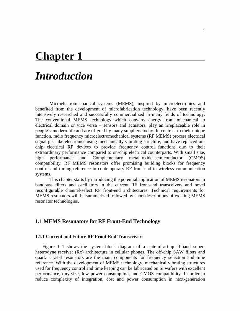
Figure 1–1 shows the system block diagram of a state-of-art quad-band super-
heterodyne receiver (Rx) architecture in cellular phones. The off-chip SAW filters and
quartz crystal resonators are the main components for frequency selection and time
reference. With the development of MEMS technology, mechanical vibrating structures
used for frequency control and time keeping can be fabricated on Si wafers with excellent
performance, tiny size, low power consumption, and CMOS compatibility. In order to
reduce complexity of integration, cost and power consumption in next-generation
2
communication systems, CMOS compatible MEMS resonators are considered as direct
replacements of these discrete components. As is indicated in the shaded area in Figure 1-
1, the receiver front-end architecture can adapt MEMS resonator technology to realize a
highly integrated system.
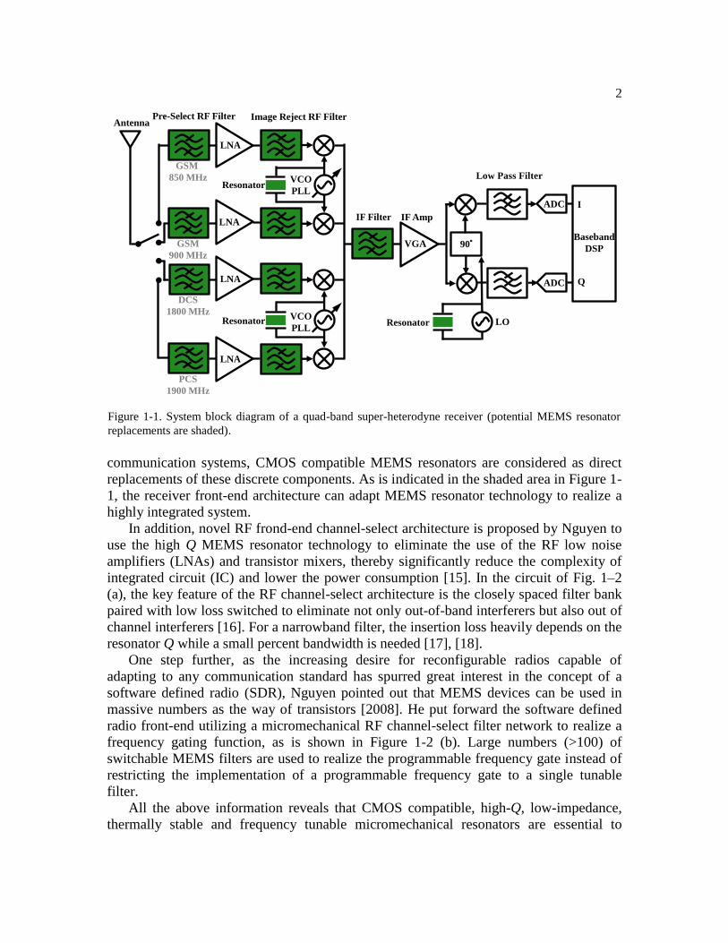
In addition, novel RF frond-end channel-select architecture is proposed by Nguyen to
use the high Q MEMS resonator technology to eliminate the use of the RF low noise
amplifiers (LNAs) and transistor mixers, thereby significantly reduce the complexity of
integrated circuit (IC) and lower the power consumption [15]. In the circuit of Fig. 1–2
(a), the key feature of the RF channel-select architecture is the closely spaced filter bank
paired with low loss switched to eliminate not only out-of-band interferers but also out of
channel interferers [16]. For a narrowband filter, the insertion loss heavily depends on the
resonator Q while a small percent bandwidth is needed [17], [18].
One step further, as the increasing desire for reconfigurable radios capable of
adapting to any communication standard has spurred great interest in the concept of a
software defined radio (SDR), Nguyen pointed out that MEMS devices can be used in
massive numbers as the way of transistors [2008]. He put forward the software defined
radio front-end utilizing a micromechanical RF channel-select filter network to realize a
frequency gating function, as is shown in Figure 1-2 (b). Large numbers (>100) of
switchable MEMS filters are used to realize the programmable frequency gate instead of
restricting the implementation of a programmable frequency gate to a single tunable
filter.
All the above information reveals that CMOS compatible, high-Q, low-impedance,
thermally stable and frequency tunable micromechanical resonators are essential to
Figure 1-1. System block diagram of a quad-band super-heterodyne receiver (potential MEMS resonator
replacements are shaded).
I
Q
VGA
Low Pass Filter
ADC
ADC
90°
LOResonator
IF Filter
Pre-Select RF FilterAntenna
GSM
850 MHz
GSM
900 MHz
DCS
1800 MHz
PCS
1900 MHz
VCO
PLLResonator
VCO
PLLResonator
LNA
LNA
LNA
LNA
Image Reject RF Filter
IF Amp
Baseband
DSP
3
construct single-chip transceiver in the near future and the highly configurable SDR
front-end in the long run.
Figure 1-2. System block diagrams for (a) a channel-select receiver architecture using integrated MEMS
filter bank and resonators, and (b) a highly-reconfigurable, low-power SDR front-end receiver utilizing a
network of large numbers of MEMS RF filters to realize a frequency gating function. (RF MEMS devices
are shaded in green).
Antenna
Multi-Band Programmable
Channel-Select Filter Network
LO
LNA Sub-Sampling
ADC
DC-bias
mode code
generator
MEMS
Resonator oscillator
Digital
Demodulation
Transistor
Switches
Digital
Output
(a)
(b)
Antenna
Multi-Band Programmable
Channel-Select MEMS RF
Filter Bank (Image Reject)
Switchable MEMS
Resonator Oscillator
VGA
ADC
Baseband
DSP
ADC
90°
LO
IF Filter
LNA
Tunable Pre-
Select Filter
I
Q
MEMS
Resonator
Oscillator
IF Amp
VCO
PLL
4
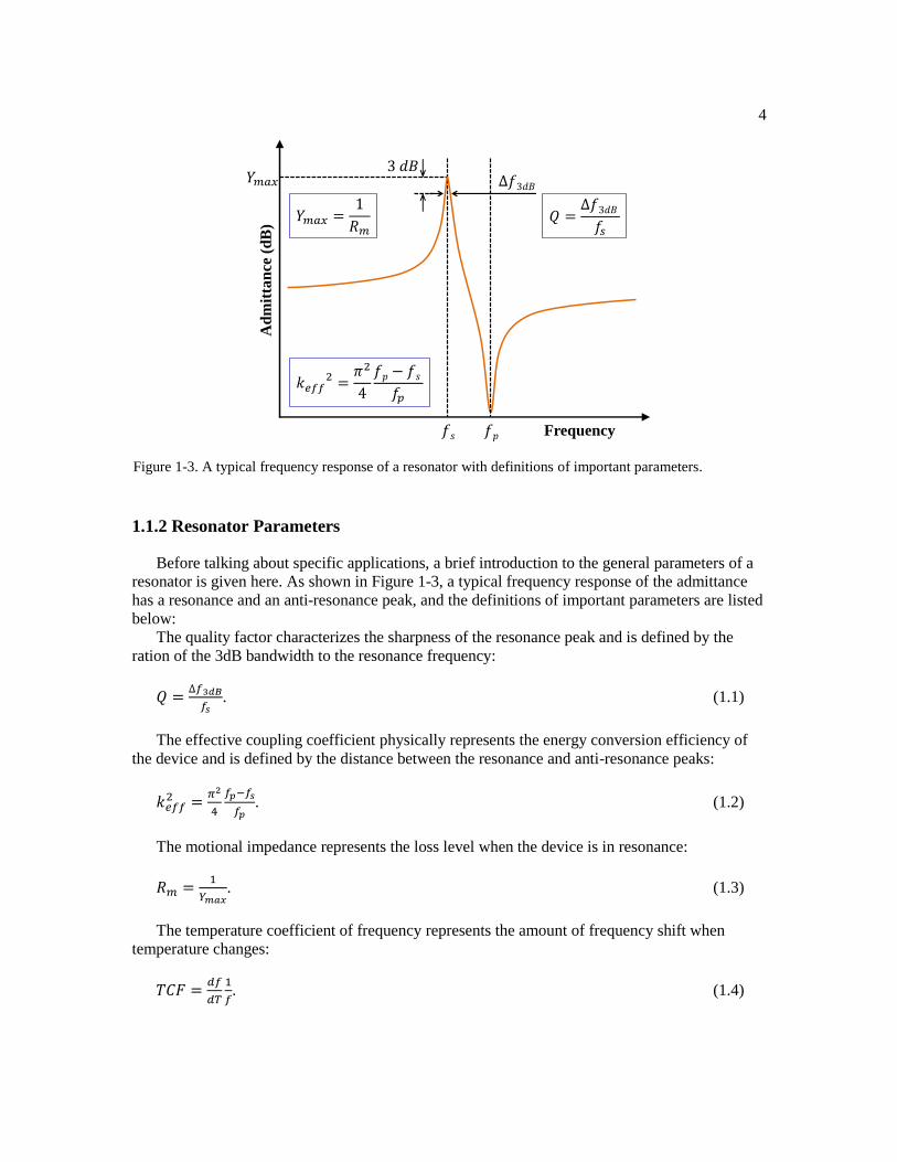
1.1.2 Resonator Parameters
Before talking about specific applications, a brief introduction to the general parameters of a
resonator is given here. As shown in Figure 1-3, a typical frequency response of the admittance
has a resonance and an anti-resonance peak, and the definitions of important parameters are listed
below:
The quality factor characterizes the sharpness of the resonance peak and is defined by the
ration of the 3dB bandwidth to the resonance frequency:
𝑄 =∆𝑓3𝑑𝐵
𝑓𝑠. (1.1)
The effective coupling coefficient physically represents the energy conversion efficiency of
the device and is defined by the distance between the resonance and anti-resonance peaks:
𝑘𝑒𝑓𝑓2 =
𝜋2
4
𝑓𝑝−𝑓𝑠
𝑓𝑝. (1.2)
The motional impedance represents the loss level when the device is in resonance:
𝑅𝑚 =1
𝑌𝑚𝑎𝑥. (1.3)
The temperature coefficient of frequency represents the amount of frequency shift when
temperature changes:
𝑇𝐶𝐹 =𝑑𝑓
𝑑𝑇
1
𝑓. (1.4)
Figure 1-3. A typical frequency response of a resonator with definitions of important parameters.
Frequency
Ad
mit
tan
ce (
dB
)
5
More introductions of these important parameters will be given in detail in the later chapters
when analyzing specific ones.
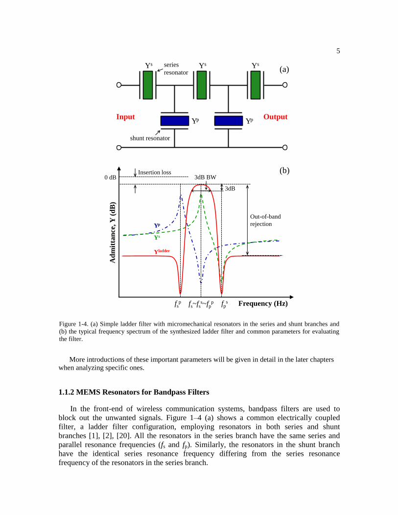
1.1.2 MEMS Resonators for Bandpass Filters
In the front-end of wireless communication systems, bandpass filters are used to
block out the unwanted signals. Figure 1–4 (a) shows a common electrically coupled
filter, a ladder filter configuration, employing resonators in both series and shunt
branches [1], [2], [20]. All the resonators in the series branch have the same series and
parallel resonance frequencies (fs and fp). Similarly, the resonators in the shunt branch
have the identical series resonance frequency differing from the series resonance
frequency of the resonators in the series branch.
Figure 1-4. (a) Simple ladder filter with micromechanical resonators in the series and shunt branches and
(b) the typical frequency spectrum of the synthesized ladder filter and common parameters for evaluating
the filter.
performanceonator replacements are shaded).
Input Output
Ys series
resonatorYs Ys
Yp Yp
shunt resonator
(a)
Frequency (Hz)
Ad
mit
tan
ce, Y
(d
B)
fs~fss~fp
pfsp fp
s
3dB
3dB BW0 dBInsertion loss
Out-of-band
rejection
Ys
Yp
Yladder
(b)
6
A typical frequency response of the ladder filter is shown in Fig. 1–4 (b). Of special
interest are the in-band insertion loss, 3dB bandwidth (BW), out-of-band rejection, the
skirts, and the shape factor. As is indicated in Figure 1-4 (b), the 3dB BW is usually set
by the effective coupling coefficient (keff2) of the series and shunt resonators. To
minimize the insertion loss of the ladder filter, the shunt resonators should have high Q
and large impedance at their parallel resonance frequency fpp and the series resonators
have high Q and low impedance (Rm) at their series resonance frequency fs.
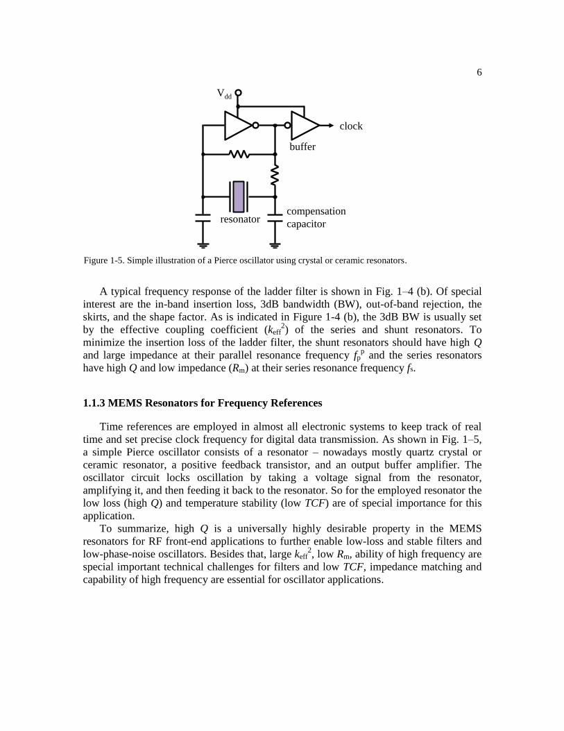
1.1.3 MEMS Resonators for Frequency References
Time references are employed in almost all electronic systems to keep track of real
time and set precise clock frequency for digital data transmission. As shown in Fig. 1–5,
a simple Pierce oscillator consists of a resonator – nowadays mostly quartz crystal or
ceramic resonator, a positive feedback transistor, and an output buffer amplifier. The
oscillator circuit locks oscillation by taking a voltage signal from the resonator,
amplifying it, and then feeding it back to the resonator. So for the employed resonator the
low loss (high Q) and temperature stability (low TCF) are of special importance for this
application.
To summarize, high Q is a universally highly desirable property in the MEMS
resonators for RF front-end applications to further enable low-loss and stable filters and
low-phase-noise oscillators. Besides that, large keff2, low Rm, ability of high frequency are
special important technical challenges for filters and low TCF, impedance matching and
capability of high frequency are essential for oscillator applications.
Figure 1-5. Simple illustration of a Pierce oscillator using crystal or ceramic resonators.
clock
resonator
buffer
compensation
capacitor
Vdd
7
1.3 MEMS Resonators
MEMS resonators can be sorted into piezoelectric and capacitive transduced ones.
Generally, the piezoelectric MEMS resonators tend to show a large coupling coefficient
and the capacitive resonators have a super high Q but a small coupling coefficient. We
will introduce the piezoelectric resonators in detail here (SAW, BAW, LWR) and then a
brief introduction to the capacitive resonators.
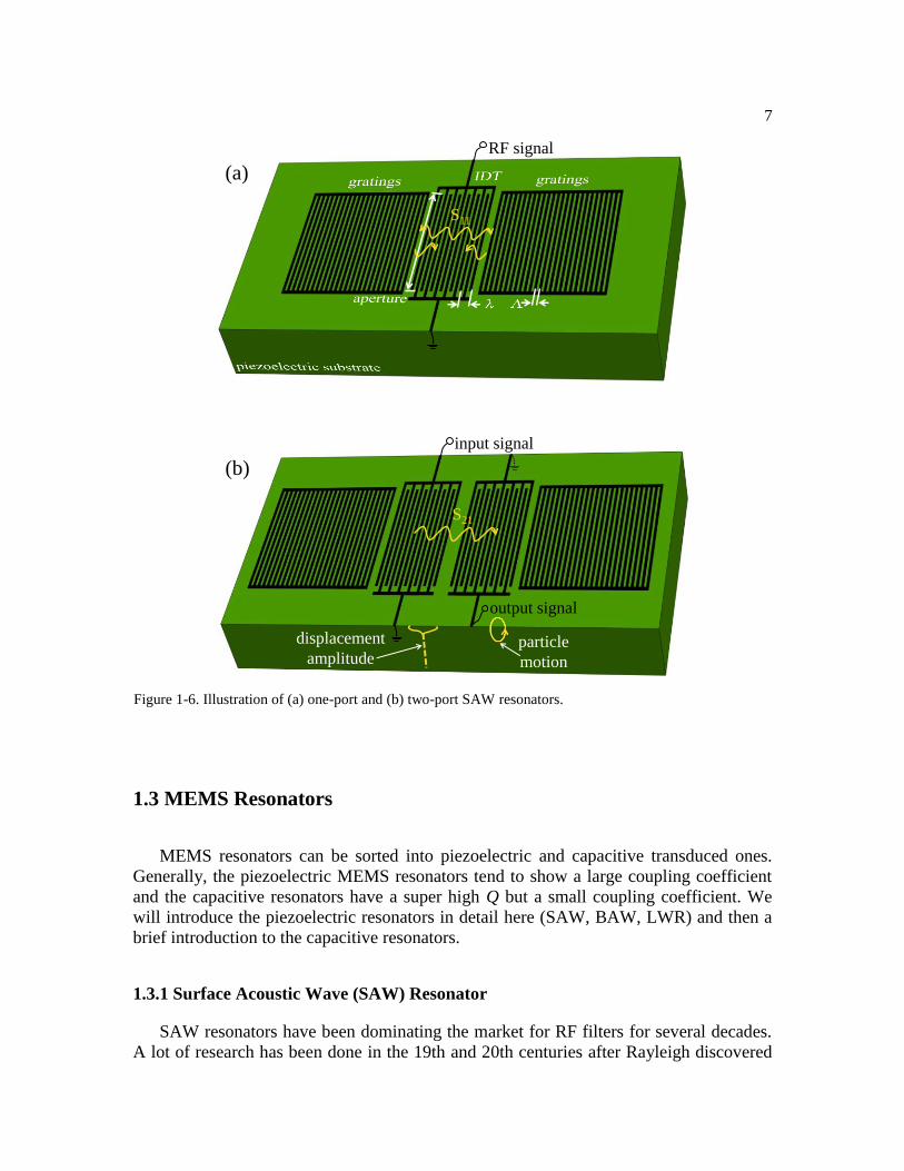
1.3.1 Surface Acoustic Wave (SAW) Resonator
SAW resonators have been dominating the market for RF filters for several decades.
A lot of research has been done in the 19th and 20th centuries after Rayleigh discovered
Figure 1-6. Illustration of (a) one-port and (b) two-port SAW resonators.
RF signal
S11
input signal
output signal
S21
displacement
amplitudeparticle
motion
(a)
(b)
8
surface acoustic waves propagating in solids in 1885 [28]. Although it remained a
scientific curiosity with very few applications for a long time, the direct generation and
detection of surface elastic waves through the piezoelectric effect led to a breakthrough in
SAW devices after the invention of an interdigital transducer (IDT) by White and
Voltmer in 1965 [29]. SAW devices have been widely used as IF and RF filters in
wireless transmission systems for several decades because of their small size, low cost,
and great performance.
Figure 1-6 shows the schematic of one-port and two-port SAW resonators composed
from piezoelectric substrate, IDT pairs, and gratings. The IDT finger width is usually
equal to quarter wavelength (λ/4) so the interdigital electrode pitch (Λ) as well as the
grating period equal half wavelength (λ/2). SAWs can be generated by applying RF
signals to the IDT and propagate on the surface of the substrate along the direction
perpendicular to the fingers. The generated SAWs would be reflected by the gratings at
both sides to reduce the energy loss.
The most severe limitation for SAW devices is that they can hardly achieve
frequencies above 2.5 GHz. SAW phase velocities of common piezoelectric substrates,
such as quartz, LiNbO3, and LiTaO3, are below 4,000 m/s, and the optical lithography
today can only achieve 0.25um line-width. Even when the frequency approaches 2G, the
shrinkage of the IDT comb-fingers makes SAW resonators vulnerable to electrostatic
discharge. Therefore, the Q factor is typically lower than 400. What’s more, the required
piezoelectric substrate is not compatible with standard microelectronic manufacturing.
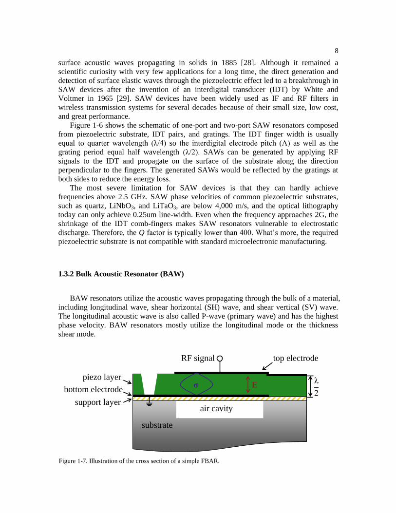
1.3.2 Bulk Acoustic Resonator (BAW)
BAW resonators utilize the acoustic waves propagating through the bulk of a material,
including longitudinal wave, shear horizontal (SH) wave, and shear vertical (SV) wave.
The longitudinal acoustic wave is also called P-wave (primary wave) and has the highest
phase velocity. BAW resonators mostly utilize the longitudinal mode or the thickness
shear mode.
Figure 1-7. Illustration of the cross section of a simple FBAR.
top electrode
bottom electrode
piezo layer
substrate
air cavity
E
RF signal
σ
support layer
9
A thin-film BAW resonator is a device composed mainly from a piezoelectric thin
film surrounded by two metal electrodes that generate the longitudinal wave propagating
according to a thickness extension mode (TE). There are mainly two ways for the wave to
be trapped in the resonator, which differentiates the two type of devices that have reached
volume manufacturing today: the FBAR and SMR.
1.3.2.1 Film Bulk Acoustic Resonator (FBAR)
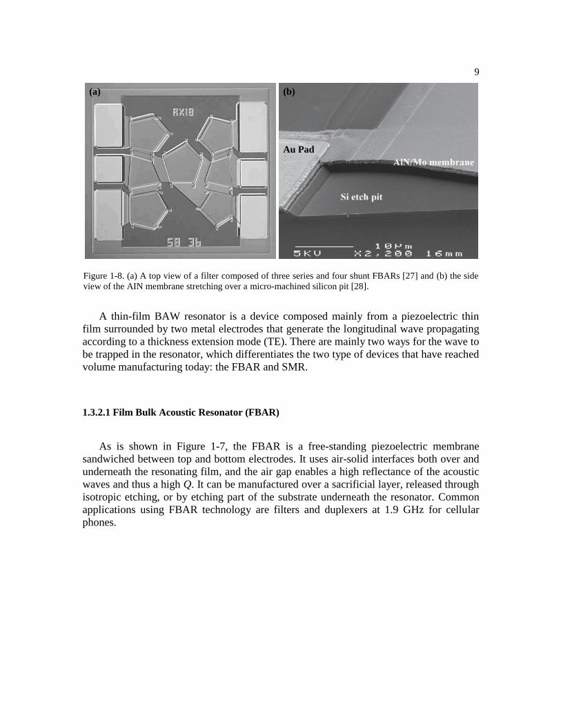
As is shown in Figure 1-7, the FBAR is a free-standing piezoelectric membrane
sandwiched between top and bottom electrodes. It uses air-solid interfaces both over and
underneath the resonating film, and the air gap enables a high reflectance of the acoustic
waves and thus a high Q. It can be manufactured over a sacrificial layer, released through
isotropic etching, or by etching part of the substrate underneath the resonator. Common
applications using FBAR technology are filters and duplexers at 1.9 GHz for cellular
phones.
Figure 1-8. (a) A top view of a filter composed of three series and four shunt FBARs [27] and (b) the side
view of the AIN membrane stretching over a micro-machined silicon pit [28].
Au Pad
(a) (b)
10
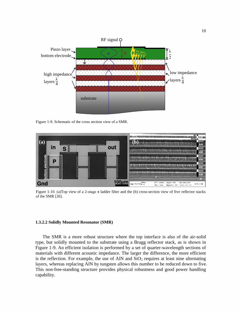
1.3.2.2 Solidly Mounted Resonator (SMR)
The SMR is a more robust structure where the top interface is also of the air-solid
type, but solidly mounted to the substrate using a Bragg reflector stack, as is shown in
Figure 1-9. An efficient isolation is performed by a set of quarter-wavelength sections of
materials with different acoustic impedance. The larger the difference, the more efficient
is the reflection. For example, the use of AlN and SiO2 requires at least nine alternating
layers, whereas replacing AlN by tungsten allows this number to be reduced down to five.
This non-free-standing structure provides physical robustness and good power handling
capability.
Figure 1-10. (a)Top view of a 2-stage π ladder filter and the (b) cross-section view of five reflector stacks
of the SMR [26].
Figure 1-9. Schematic of the cross section view of a SMR.
(a) (b)
high impedance
layers
low impedance
layers
substrate
bottom electrode
Piezo layerEσ
RF signal
11
1.3.3 Lamb Wave Resonator (LWR)
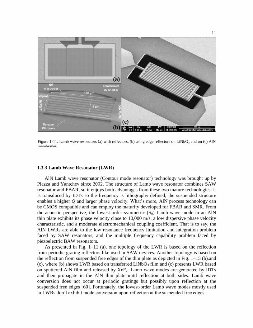
AlN Lamb wave resonator (Contour mode resonator) technology was brought up by
Piazza and Yantchev since 2002. The structure of Lamb wave resonator combines SAW
resonator and FBAR, so it enjoys both advantages from these two mature technologies: it
is transduced by IDTs so the frequency is lithography defined; the suspended structure
enables a higher Q and larger phase velocity. What’s more, AlN process technology can
be CMOS compatible and can employ the maturity developed for FBAR and SMR. From
the acoustic perspective, the lowest-order symmetric (S0) Lamb wave mode in an AlN
thin plate exhibits its phase velocity close to 10,000 m/s, a low dispersive phase velocity
characteristic, and a moderate electromechanical coupling coefficient. That is to say, the
AlN LWRs are able to the low resonance frequency limitation and integration problem
faced by SAW resonators, and the multiple frequency capability problem faced by
piezoelectric BAW resonators.
As presented in Fig. 1–11 (a), one topology of the LWR is based on the reflection
from periodic grating reflectors like used in SAW devices. Another topology is based on
the reflection from suspended free edges of the thin plate as depicted in Fig. 1–15 (b).and
(c), where (b) shows LWR based on transferred LiNbO3 film and (c) presents LWR based
on sputtered AlN film and released by XeF2. Lamb wave modes are generated by IDTs
and then propagate in the AlN thin plate until reflection at both sides. Lamb wave
conversion does not occur at periodic gratings but possibly upon reflection at the
suspended free edges [60]. Fortunately, the lowest-order Lamb wave modes mostly used
in LWRs don’t exhibit mode conversion upon reflection at the suspended free edges.
Figure 1-11. Lamb wave resonators (a) with reflectors, (b) using edge reflectors on LiNbO3 and on (c) AlN
membranes.
(a)
(b)(c)
12
1.3.4 Electrostatic Resonators
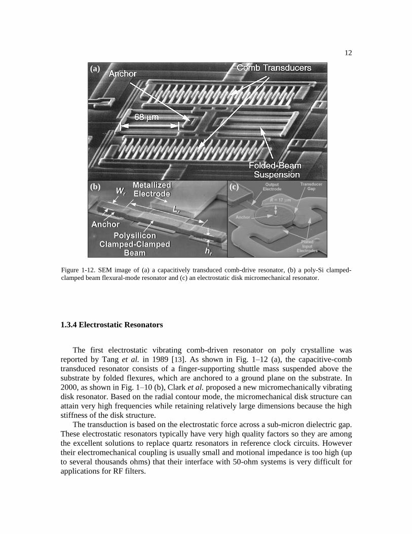
The first electrostatic vibrating comb-driven resonator on poly crystalline was
reported by Tang et al. in 1989 [13]. As shown in Fig. 1–12 (a), the capacitive-comb
transduced resonator consists of a finger-supporting shuttle mass suspended above the
substrate by folded flexures, which are anchored to a ground plane on the substrate. In
2000, as shown in Fig. 1–10 (b), Clark et al. proposed a new micromechanically vibrating
disk resonator. Based on the radial contour mode, the micromechanical disk structure can
attain very high frequencies while retaining relatively large dimensions because the high
stiffness of the disk structure.
The transduction is based on the electrostatic force across a sub-micron dielectric gap.
These electrostatic resonators typically have very high quality factors so they are among
the excellent solutions to replace quartz resonators in reference clock circuits. However
their electromechanical coupling is usually small and motional impedance is too high (up
to several thousands ohms) that their interface with 50-ohm systems is very difficult for
applications for RF filters.
Figure 1-12. SEM image of (a) a capacitively transduced comb-drive resonator, (b) a poly-Si clamped-
clamped beam flexural-mode resonator and (c) an electrostatic disk micromechanical resonator.
(a)
(b) (c)
13
1.4 Report Outline
This report is organized into five chapters about the AlN RF telemetry components.
Chapter 1 contains the research motivation, technical challenges, and existing solutions.
Chapter 2 provides the fundamentals of propagating characteristics of Lamb wave modes
in AlN membranes. Resonator basics, design, modeling, and fabrication process are
presented in Chapter 3. Chapter 4 focuses on the analysis, design, simulation and testing
result of high Q AlN LWRs using butterfly-shaped plates. Finally, Chapter 5 will
conclude this research work.
14
Chapter 2
Lamb Wave propagating in AlN film
Piezoelectric thin films have been utilized in SAW and BAW filters mainly because
of the efficient electromechanical transduction. Lamb wave in piezoelectric thin plates
has drawn great attentions due to its high phase velocity. In this chapter, a study of the
lowest-order Lamb wave modes (S0 modes) in an AlN plate is presented. Phase
velocities, electromechanical coupling coefficients, and dispersion characteristics of TCF
of Lamb waves will be included in the theoretical studies.
2.1 Aluminum Nitride (AlN)
AlN emerged as the most suitable technology for the transduction of acoustic waves
for RF applications because it is an excellent compromise between performance and
manufacturability. Although its coupling coefficient is not as high as that of ZnO, PZT or
LiNbO3, it has high acoustic velocity, high thermal conductivity, low acoustic loss,
Table 2-1. Physical properties of ZnO, AlN, and LiNbO3 [27].
ZnO AlN LiNbO3 Units
Density 5680 3260 4700 (kg/m3)
Longitudinal acoustic wave velocity ~6350 ~11300 ~6550 (m/s)
Shear acoustic wave velocity ~2720 ~6000 ~3590 (m/s)
Lattice constant, c 3.249 3.112 13.863 (Å)
Lattice constant, a 5.206 4.982 5.150 (Å)
Piezoelectric coefficient, e15 –0.48 –0.48 3.69 (C/m2)
Piezoelectric coefficient, e31 –0.57 –0.58 0.3 (C/m2)
Piezoelectric coefficient, e33 1.32 1.55 1.77 (C/m2)
Thermal expansion (300 K) 2.92 4.15 5~15 (10–6
/°C)
Thermal conductivity 60 280 5.6 (W/mK)
TCF –60 –25 –58~-90 (ppm/°C)
15
chemical stability and relatively low TCF, as is shown in Table 2-1. These properties
enable the MEMS resonators featuring the ability of high frequency, excellent power
handling capability, high Q, functionality in harsh environment, and limited drift with
temperature.
As illustrated in Fig. 2–1, AlN is wurtzite-structured material with c-axis, belonging
to hexagonal crystal system, with polarized direction along the c-axis (0001) which is
usually normal to the substrate.
Another advantage of AlN is the low process temperature and the fact that it does not
contain any contaminating elements harmful for semiconductor devices, unlike most
other piezoelectric materials. This is essential in the case of monolithic integration of
MEMS resonators with microelectronic integrated circuits. Reactive sputtering from a
pure Al target in a plasma containing nitrogen is the most suitable method to obtain
crystalline AlN films with sufficient quality for MEMS resonator applications at a
deposition temperature lower than 400. Figure 2-2 shows the cross section of such an
AlN film grown in pulsed DC mode. The microstructure is typical, with very densely
packed columnar grains. The parameters of the AlN deposition process have to be
optimized in order to ensure that a vast majority of grains are oriented along the c-axis
since the spontaneous polarization of AlN, and hence the maximum piezoelectric effect,
is parallel to that direction.
Figure 2-1. Hexagonal wurtzite crystal structure of AlN.
a-axis
c-axis
Al N
a = 3.11 Å
c = 4.98 Å(0001)
16
2.2 Piezoelectric Effect and its Constitutive Equations
“Piezoelectricity” is derived from the Greek word “piezein”, meaning “to press”,
meaning that crystal that acquire charge when being compressed, twisted, or distorted are
said to be piezoelectric. The physical origin of piezoelectricity comes from the charge
asymmetry within the primitive unit cell which results in the formation of a net electric
dipole. The polar axis is an imaginary line pointing through the center of the negative and
positive charge in the dipole. As is shown in Figure 2-3 is examples of how the
piezoelectricity (here the piezoelectric strain parameter d-coefficients are used) relates the
force and charge of a piezoelectric block.
In the mechanical domain of a linear elastic material the Hooke’s Law dominates:
𝑇 = 𝑐𝑆 or 𝑆 = 𝑠𝑇, (2.1)
where c is the elastic stiffness constant, s is the elastic compliance constant, T and stress
tensor and S is the strain tensor.
In the electrical domain, the dielectric constant relates the charge density
displacement vector D and electric field vector E,
𝐷 = 𝜀𝐸 or 𝐸 = 𝛽𝐷, (2.2)
Where 𝜀 is the dielectric permittivity constant and 𝛽 is the dielectric impermittivity
constant.
Figure 2-2. Hexagonal wurtzite crystal structure of AlN.
17
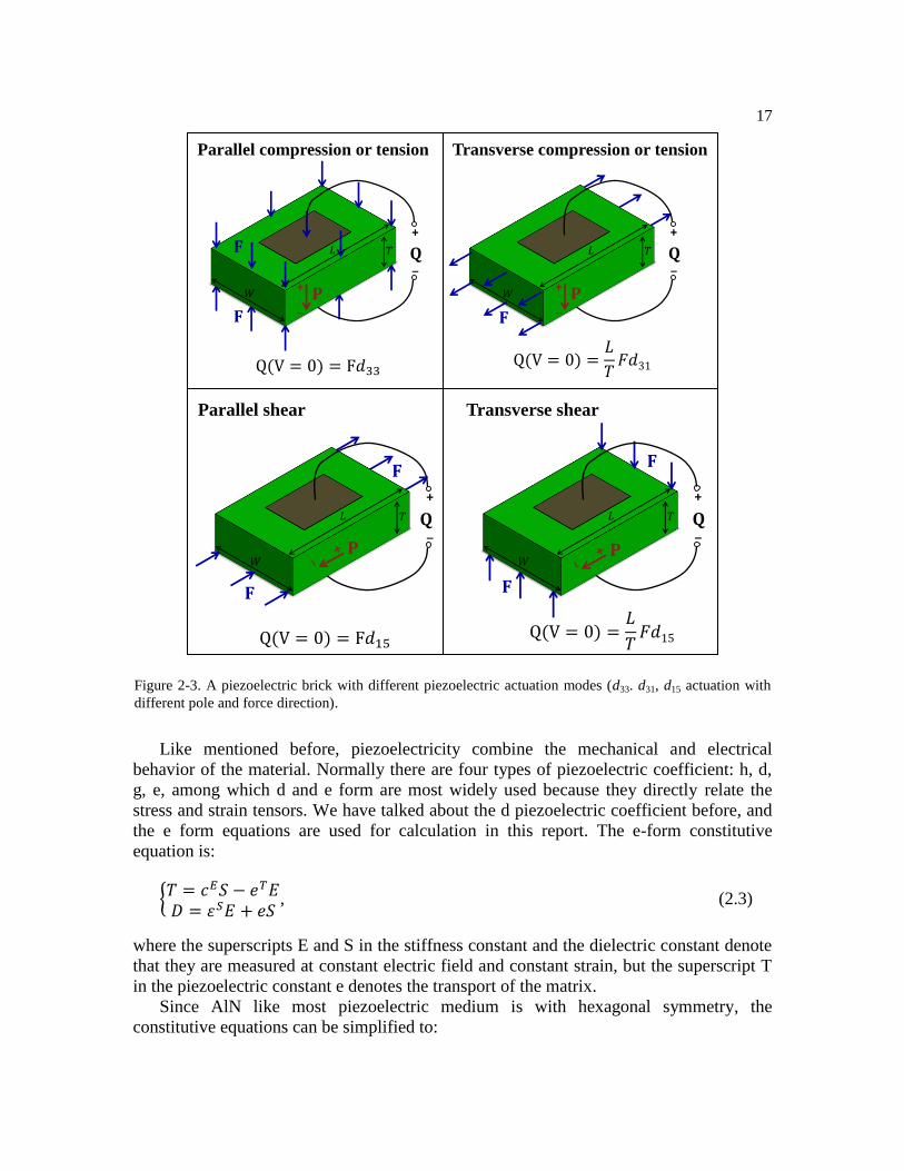
Like mentioned before, piezoelectricity combine the mechanical and electrical
behavior of the material. Normally there are four types of piezoelectric coefficient: h, d,
g, e, among which d and e form are most widely used because they directly relate the
stress and strain tensors. We have talked about the d piezoelectric coefficient before, and
the e form equations are used for calculation in this report. The e-form constitutive
equation is:
𝑇 = 𝑐𝐸𝑆 − 𝑒𝑇𝐸𝐷 = 𝜀𝑆𝐸 + 𝑒𝑆
, (2.3)
where the superscripts E and S in the stiffness constant and the dielectric constant denote
that they are measured at constant electric field and constant strain, but the superscript T
in the piezoelectric constant e denotes the transport of the matrix.
Since AlN like most piezoelectric medium is with hexagonal symmetry, the
constitutive equations can be simplified to:
Figure 2-3. A piezoelectric brick with different piezoelectric actuation modes (d33. d31, d15 actuation with
different pole and force direction).
+
_Q
+
_P
F
Parallel compression or tension
+
_Q
+
_P
F
Transverse compression or tension
F
+
_Q
P
F
Parallel shear
+
_Q
F
Transverse shear
P
FF
18
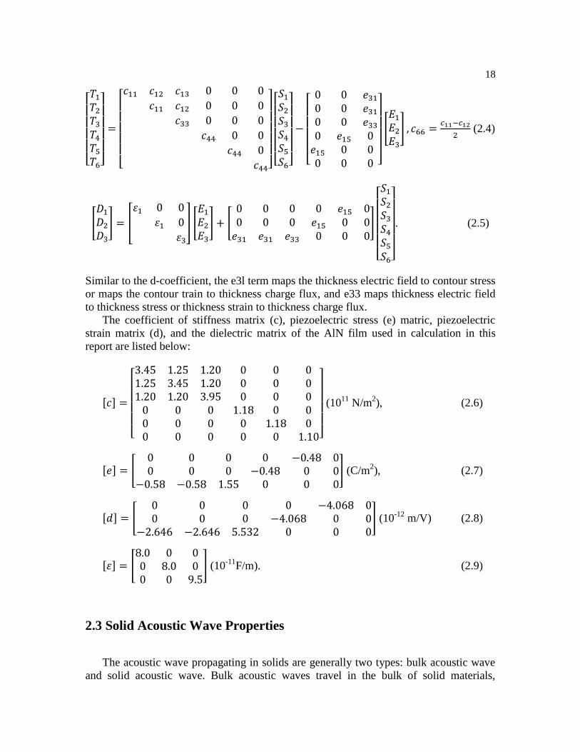
[ 𝑇1
𝑇2
𝑇3
𝑇4
𝑇5
𝑇6]
=
[ 𝑐11 𝑐12 𝑐13 0 0 0
𝑐11 𝑐12 0 0 0
𝑐33 0 0 0
𝑐44 0 0
𝑐44 0
𝑐44]
[ 𝑆1
𝑆2
𝑆3
𝑆4
𝑆5
𝑆6]
−
[
0 0 𝑒31
0 0 𝑒31
0 0 𝑒33
0 𝑒15 0𝑒15 0 00 0 0 ]
[𝐸1
𝐸2
𝐸3
] , 𝑐66 =𝑐11−𝑐12
2 (2.4)
[𝐷1
𝐷2
𝐷3
] = [
𝜀1 0 0
𝜀1 0
𝜀3
] [𝐸1
𝐸2
𝐸3
] + [
0 0 0 0 𝑒15 00 0 0 𝑒15 0 0
𝑒31 𝑒31 𝑒33 0 0 0]
[ 𝑆1
𝑆2
𝑆3
𝑆4
𝑆5
𝑆6]
. (2.5)
Similar to the d-coefficient, the e3l term maps the thickness electric field to contour stress
or maps the contour train to thickness charge flux, and e33 maps thickness electric field
to thickness stress or thickness strain to thickness charge flux.
The coefficient of stiffness matrix (c), piezoelectric stress (e) matric, piezoelectric
strain matrix (d), and the dielectric matrix of the AlN film used in calculation in this
report are listed below:
[𝑐] =
[ 3.45 1.25 1.20 0 0 01.25 3.45 1.20 0 0 01.20 1.20 3.95 0 0 00 0 0 1.18 0 00 0 0 0 1.18 00 0 0 0 0 1.10]
(1011
N/m2), (2.6)
[𝑒] = [0 0 0 0 −0.48 00 0 0 −0.48 0 0
−0.58 −0.58 1.55 0 0 0] (C/m
2), (2.7)
[𝑑] = [0 0 0 0 −4.068 00 0 0 −4.068 0 0
−2.646 −2.646 5.532 0 0 0] (10
-12 m/V) (2.8)
[𝜀] = [8.0 0 00 8.0 00 0 9.5
] (10-11
F/m). (2.9)
2.3 Solid Acoustic Wave Properties
The acoustic wave propagating in solids are generally two types: bulk acoustic wave
and solid acoustic wave. Bulk acoustic waves travel in the bulk of solid materials,
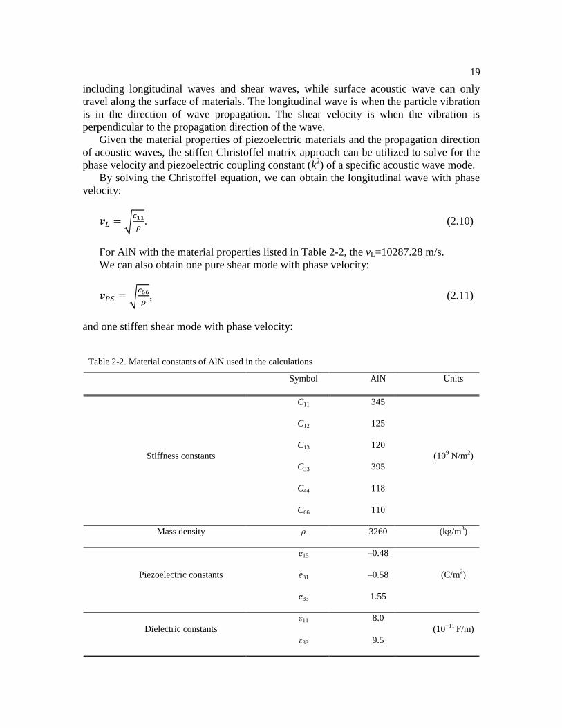
19
including longitudinal waves and shear waves, while surface acoustic wave can only
travel along the surface of materials. The longitudinal wave is when the particle vibration
is in the direction of wave propagation. The shear velocity is when the vibration is
perpendicular to the propagation direction of the wave.
Given the material properties of piezoelectric materials and the propagation direction
of acoustic waves, the stiffen Christoffel matrix approach can be utilized to solve for the
phase velocity and piezoelectric coupling constant (k2) of a specific acoustic wave mode.
By solving the Christoffel equation, we can obtain the longitudinal wave with phase
velocity:
𝑣𝐿 = √𝑐11
𝜌. (2.10)
For AlN with the material properties listed in Table 2-2, the vL=10287.28 m/s.
We can also obtain one pure shear mode with phase velocity:
𝑣𝑃𝑆 = √𝑐66
𝜌, (2.11)
and one stiffen shear mode with phase velocity:
Table 2-2. Material constants of AlN used in the calculations
Symbol AlN Units
Stiffness constants
C11 345
(109 N/m
2)
C12 125
C13 120
C33 395
C44 118
C66 110
Mass density ρ 3260 (kg/m3)
Piezoelectric constants
e15 –0.48
(C/m2) e31 –0.58
e33 1.55
Dielectric constants
ε11 8.0
(10−11
F/m)
ε33 9.5
20
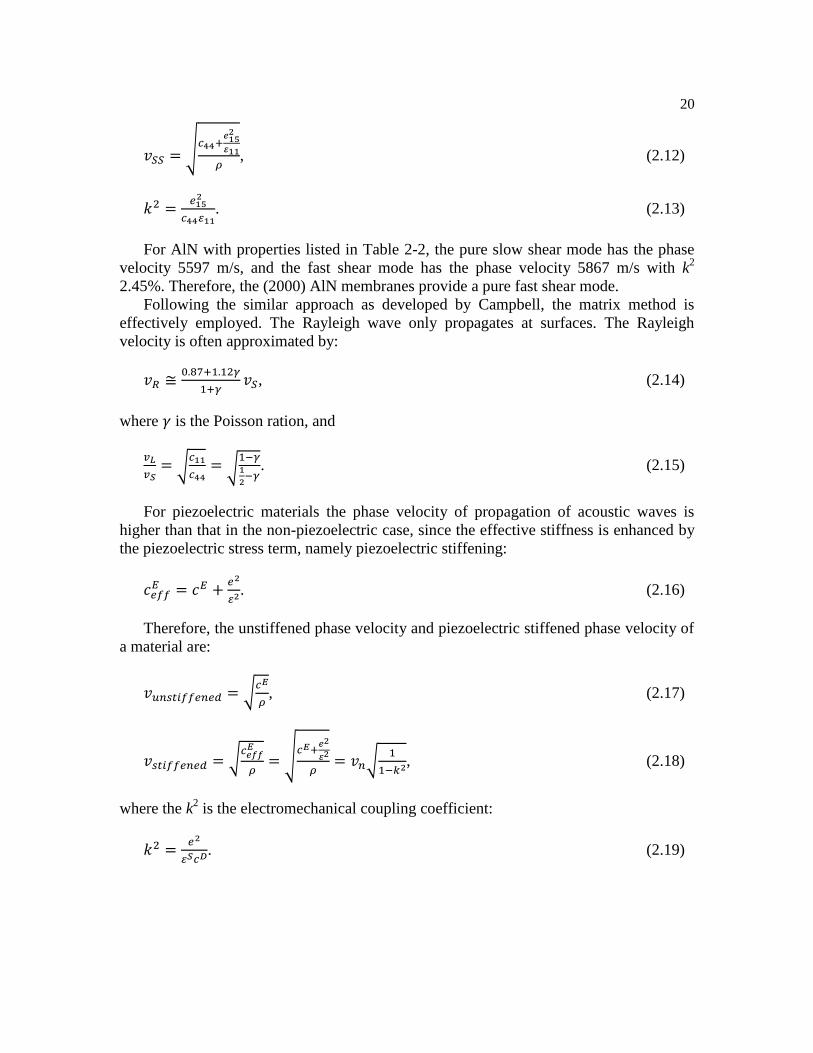
𝑣𝑆𝑆 = √𝑐44+𝑒152
𝜀11
𝜌, (2.12)
𝑘2 =𝑒15
2
𝑐44𝜀11. (2.13)
For AlN with properties listed in Table 2-2, the pure slow shear mode has the phase
velocity 5597 m/s, and the fast shear mode has the phase velocity 5867 m/s with k2
2.45%. Therefore, the (2000) AlN membranes provide a pure fast shear mode.
Following the similar approach as developed by Campbell, the matrix method is
effectively employed. The Rayleigh wave only propagates at surfaces. The Rayleigh
velocity is often approximated by:
𝑣𝑅 ≅0.87+1.12𝛾
1+𝛾𝑣𝑆, (2.14)
where 𝛾 is the Poisson ration, and
𝑣𝐿
𝑣𝑆= √
𝑐11
𝑐44= √
1−𝛾1
2−𝛾
. (2.15)
For piezoelectric materials the phase velocity of propagation of acoustic waves is
higher than that in the non-piezoelectric case, since the effective stiffness is enhanced by
the piezoelectric stress term, namely piezoelectric stiffening:
𝑐𝑒𝑓𝑓𝐸 = 𝑐𝐸 +
𝑒2
𝜀2. (2.16)
Therefore, the unstiffened phase velocity and piezoelectric stiffened phase velocity of
a material are:
𝑣𝑢𝑛𝑠𝑡𝑖𝑓𝑓𝑒𝑛𝑒𝑑 = √𝑐𝐸
𝜌, (2.17)
𝑣𝑠𝑡𝑖𝑓𝑓𝑒𝑛𝑒𝑑 = √𝑐𝑒𝑓𝑓𝐸
𝜌= √𝑐𝐸+
𝑒2
𝜀2
𝜌= 𝑣𝑛√
1
1−𝑘2, (2.18)
where the k2 is the electromechanical coupling coefficient:
𝑘2 =𝑒2
𝜀𝑆𝑐𝐷. (2.19)
21
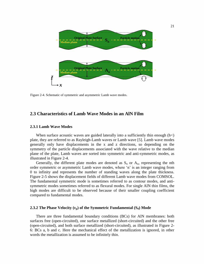
2.3 Characteristics of Lamb Wave Modes in an AlN Film
2.3.1 Lamb Wave Modes
When surface acoustic waves are guided laterally into a sufficiently thin enough (h<)
plate, they are referred to as Rayleigh-Lamb waves or Lamb wave [5]. Lamb wave modes
generally only have displacements in the x and z directions, so depending on the
symmetry of the particle displacements associated with the wave relative to the median
plane of the plate, Lamb waves are sorted into symmetric and anti-symmetric modes, as
illustrated in Figure 2-4.
Generally, the different plate modes are denoted as Sn or An, representing the nth
order symmetric or asymmetric Lamb wave modes, where ‘n’ is an integer ranging from
0 to infinity and represents the number of standing waves along the plate thickness.
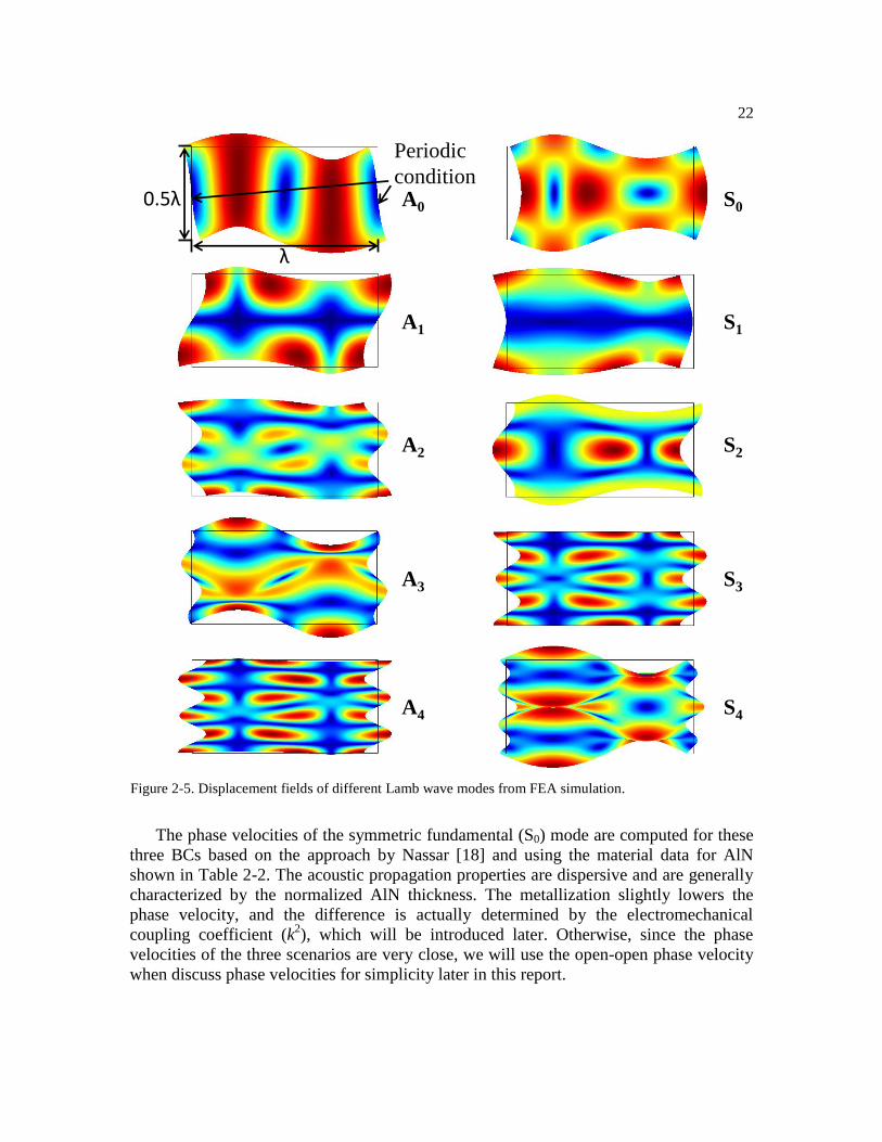
Figure 2-5 shows the displacement fields of different Lamb wave modes from COMSOL.
The fundamental symmetric mode is sometimes referred to as contour modes, and anti-
symmetric modes sometimes referred to as flexural modes. For single AlN thin films, the
high modes are difficult to be observed because of their smaller coupling coefficient
compared to fundamental modes.
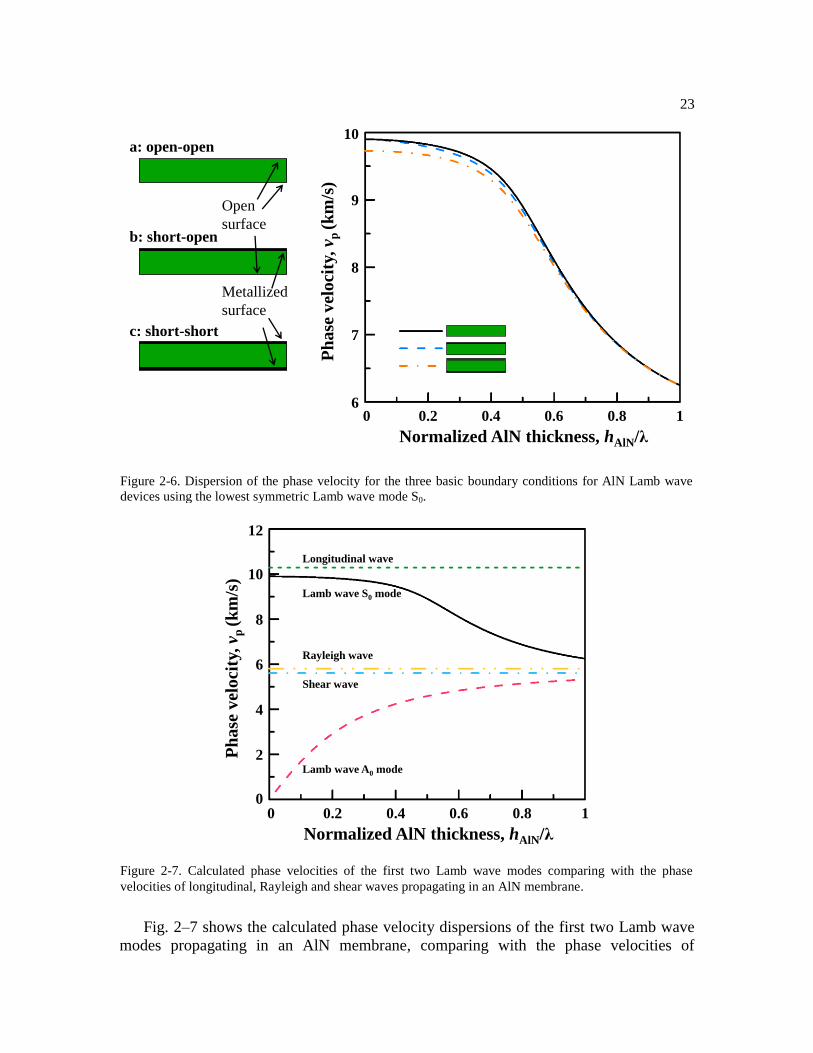
2.3.2 The Phase Velocity (vp) of the Symmetric Fundamental (S0) Mode
There are three fundamental boundary conditions (BCs) for AlN membranes: both
surfaces free (open-circuited), one surface metallized (short-circuited) and the other free
(open-circuited), and both surface metallized (short-circuited), as illustrated in Figure 2-
6: BCs a, b and c. Here the mechanical effect of the metallization is ignored, in other
words the metallization is assumed to be infinitely thin.
Figure 2-4. Schematic of symmetric and asymmetric Lamb wave modes.
Particle motionOriginal Plate SurfaceSnMedian plane
Particle motionOriginal Plate SurfaceAnMedian plane
x
z
22
The phase velocities of the symmetric fundamental (S0) mode are computed for these
three BCs based on the approach by Nassar [18] and using the material data for AlN
shown in Table 2-2. The acoustic propagation properties are dispersive and are generally
characterized by the normalized AlN thickness. The metallization slightly lowers the
phase velocity, and the difference is actually determined by the electromechanical
coupling coefficient (k2), which will be introduced later. Otherwise, since the phase
velocities of the three scenarios are very close, we will use the open-open phase velocity
when discuss phase velocities for simplicity later in this report.
Figure 2-5. Displacement fields of different Lamb wave modes from FEA simulation.
A0
A1
A2
A3
A4
S0
S1
S2
S3
S4
λ
0.5λ
Periodic
condition
23
Fig. 2–7 shows the calculated phase velocity dispersions of the first two Lamb wave
modes propagating in an AlN membrane, comparing with the phase velocities of
Figure 2-7. Calculated phase velocities of the first two Lamb wave modes comparing with the phase
velocities of longitudinal, Rayleigh and shear waves propagating in an AlN membrane.
Figure 2-6. Dispersion of the phase velocity for the three basic boundary conditions for AlN Lamb wave
devices using the lowest symmetric Lamb wave mode S0.
0
2
0.2 0.4 0.6 0.8 1
Normalized AlN thickness, hAlN/λ
8
6
4
12
10
0
Ph
ase
vel
oci
ty, v p
(km
/s)
Longitudinal wave
Lamb wave S0 mode
Lamb wave A0 mode
Rayleigh wave
Shear wave
Metallized
surface
Open
surface
a: open-open
b: short-open
c: short-short
06
0.2 0.4 0.6 0.8 1
Normalized AlN thickness, hAlN/λ
9
8
7
10
Ph
ase
vel
oci
ty, v p
(km
/s)
24
longitudinal, Rayleigh and shear waves in AlN. The S0 Lamb wave mode shows a phase
velocity near 10000 m/s which is close to the phase velocity of longitudinal wave
(BAW), and it exhibits much weaker phase velocity dispersion than the A0 Lamb wave
mode. The high phase velocity of the S0 mode in an AlN plate is suitable for high
frequency devices and the weak phase velocity dispersion is preferred for fabrication
robustness. When the plate is becoming thick, both the phase velocities of the A0 and S0
Lamb wave modes approaches that of Rayleigh mode.
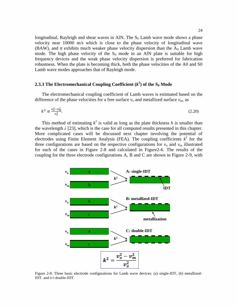
2.3.3 The Electromechanical Coupling Coefficient (k2) of the S0 Mode
The electromechanical coupling coefficient of Lamb waves is estimated based on the
difference of the phase velocities for a free surface vo and metallized surface vm, as
𝑘2 ≅𝑣𝑜
2−𝑣𝑚2
𝑣𝑜2 . (2.20)
This method of estimating k2 is valid as long as the plate thickness h is smaller than
the wavelength λ [23], which is the case for all computed results presented in this chapter.
More complicated cases will be discussed next chapter involving the potential of
electrodes using Finite Element Analysis (FEA). The coupling coefficients k2 for the
three configurations are based on the respective configurations for vo and vm illustrated
for each of the cases in Figure 2-8 and calculated in Figure2-6. The results of the
coupling for the three electrode configurations A, B and C are shown in Figure 2-9, with
Figure 2-8. Three basic electrode configurations for Lamb wave devices: (a) single-IDT, (b) metallized-
IDT, and (c) double-IDT.
vo
vm
vo
vm
vo
vm
IDT
metallization
A: single-IDT
B: metallized-IDT
C: double-IDT
k2
k2
k2
a
a
b
b
c
c
25
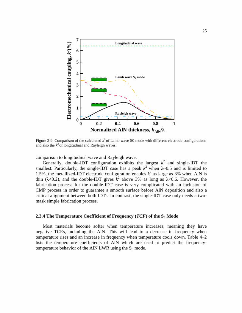
comparison to longitudinal wave and Rayleigh wave.
Generally, double-IDT configuration exhibits the largest k2 and single-IDT the
smallest. Particularly, the single-IDT case has a peak k2 when λ~0.5 and is limited to
1.5%, the metallized-IDT electrode configuration enables k2 as large as 3% when AlN is
thin (λ<0.2), and the double-IDT gives k2 above 3% as long as λ<0.6. However, the
fabrication process for the double-IDT case is very complicated with an inclusion of
CMP process in order to guarantee a smooth surface before AlN deposition and also a
critical alignment between both IDTs. In contrast, the single-IDT case only needs a two-
mask simple fabrication process.
2.3.4 The Temperature Coefficient of Frequency (TCF) of the S0 Mode
Most materials become softer when temperature increases, meaning they have
negative TCEs, including the AlN. This will lead to a decrease in frequency when
temperature rises and an increase in frequency when temperature cools down. Table 4–2
lists the temperature coefficients of AlN which are used to predict the frequency-
temperature behavior of the AlN LWR using the S0 mode.
Figure 2-9. Comparison of the calculated k2 of Lamb wave S0 mode with different electrode configurations
and also the k2
of longitudinal and Rayleigh waves.
00
1
3
0.2 0.4 0.6 0.8 1
Normalized AlN thickness, hAlN/λ
Ele
ctro
mec
ha
nic
al
cou
pli
ng
, k
2(%
)
6
7Longitudinal wave
Lamb wave S0 mode
Rayleigh wave
5
4
2
26
The frequency drift of the AlN LWR not only dependent on the changes in the
stiffness constants with temperature and but also the thermal expansion coefficients.
Under linear approximation of the temperature dependence of the stiffness constants, the
TCF of the AlN LWR is:
Table 2-3. Temperature coefficients of material constants of AlN used in the calculations. [50]
Symbol AlN Units
Temperature
coefficients of stiffness
constants
TC11 –37
(10–6
1/°C)
TC12 –1.8
TC13 –1.8
TC33 –65
TC44 –50
TC66 –57
Thermal expansion
coefficients
α11 5.27
(10–6
1/°C)
α33 4.15
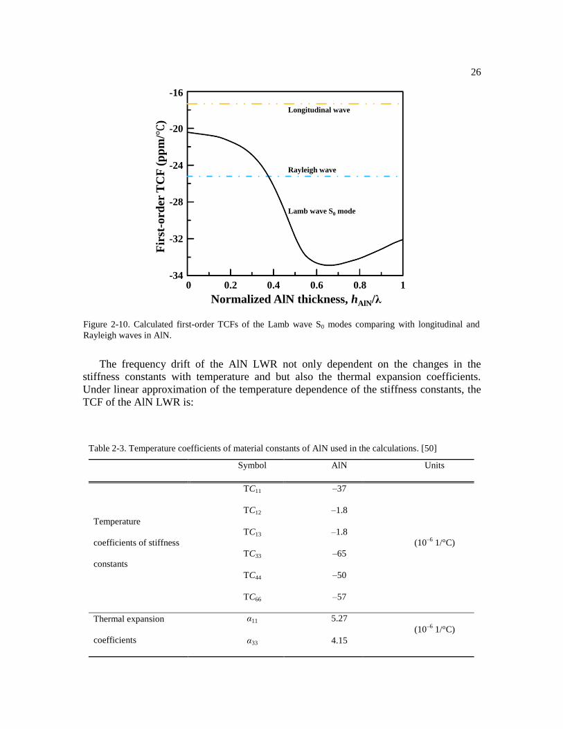
Figure 2-10. Calculated first-order TCFs of the Lamb wave S0 modes comparing with longitudinal and
Rayleigh waves in AlN.
0-34
-28
0.2 0.4 0.6 0.8 1
Normalized AlN thickness, hAlN/λ
-20
-16
Longitudinal wave
Lamb wave S0 mode
Rayleigh wave-24
-32
Fir
st-o
rder
TC
F (
pp
m/
)
27
𝑇𝐶𝐹1𝑠𝑡 =1
𝑣𝑝
𝜕𝑣𝑝
𝜕𝑇− 𝛼𝑥
=1
𝑣𝑝
𝑣𝑝(𝑇0+∆𝑇)−𝑣𝑝(𝑇0)
∆𝑇− 𝛼𝑥, (2.21)
where 𝑣𝑝(𝑇0) is calculated from the material constants in Table 2-3, and 𝑣𝑝(𝑇0 + ∆𝑇) is
calculated based on the new stiffness matrix 𝑐𝑖𝑗(𝑇0 + ∆𝑇):
𝑐𝑖𝑗(𝑇0 + ∆𝑇) = 𝑐𝑖𝑗(𝑇0)(1 + 𝑇𝐶𝐸𝑖𝑗). (2.22)
The TCF of the AlN LWR can be theoretically predicted using the above formulas and the
temperature dependence of material coefficients listed in Table 2–3. Since there are only first-
order temperature coefficients of stiffness constants available in the literature [66], all theoretical
calculations only considers the first-order effect on the TCF in this study. The calculated first-
order TCFs of the Lamb wave S0 modes comparing with longitudinal and Rayleigh waves in AlN
are shown in Fig. 2–10. The AlN LWR using the S0 mode shows a theoretical TCF range from -
33 to –22 ppm/°C which is close to the experimental results [58]. What’s more, it is interesting to
note that the first-order TCF shows a dispersive characteristic and reaches the worst case when
the AlN membrane thickness is around 0.62λ.
28
Chapter 3
Design of AlN Lamb Wave
Resonators Utilizing S0 Mode
3.1 Equivalent Circuit and Typical Frequency Response
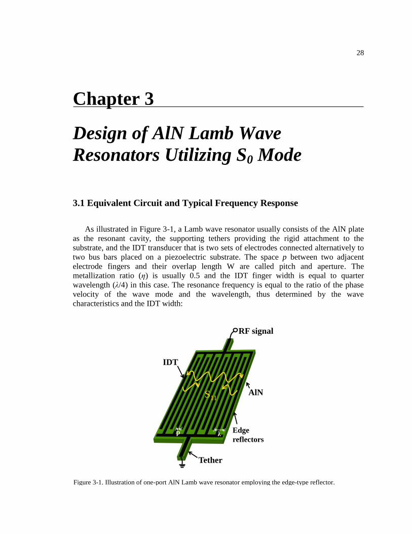
As illustrated in Figure 3-1, a Lamb wave resonator usually consists of the AlN plate
as the resonant cavity, the supporting tethers providing the rigid attachment to the
substrate, and the IDT transducer that is two sets of electrodes connected alternatively to
two bus bars placed on a piezoelectric substrate. The space p between two adjacent
electrode fingers and their overlap length W are called pitch and aperture. The
metallization ratio (η) is usually 0.5 and the IDT finger width is equal to quarter
wavelength (λ/4) in this case. The resonance frequency is equal to the ratio of the phase
velocity of the wave mode and the wavelength, thus determined by the wave
characteristics and the IDT width:
Figure 3-1. Illustration of one-port AlN Lamb wave resonator employing the edge-type reflector.
p λ
S11
IDT
Edge
reflectors
AlN
Tether
RF signal
29
𝑓𝑠 =𝑣𝑝
𝜆=
𝑣𝑝
2𝑝. (3.1)
A piezoelectric resonator usually can be described using the Butterworth-Van Dyke
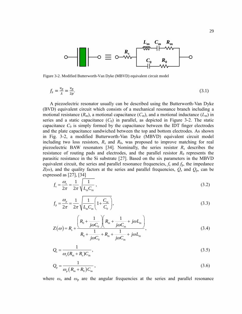
(BVD) equivalent circuit which consists of a mechanical resonance branch including a
motional resistance (Rm), a motional capacitance (Cm), and a motional inductance (Lm) in
series and a static capacitance (C0) in parallel, as depicted in Figure 3-2. The static
capacitance C0 is simply formed by the capacitance between the IDT finger electrodes
and the plate capacitance sandwiched between the top and bottom electrodes. As shown
in Fig. 3-2, a modified Butterworth-Van Dyke (MBVD) equivalent circuit model
including two loss resistors, Rs and R0, was proposed to improve matching for real
piezoelectric BAW resonators [34]. Nominally, the series resistor Rs describes the
resistance of routing pads and electrodes, and the parallel resistor R0 represents the
parasitic resistance in the Si substrate [27]. Based on the six parameters in the MBVD
equivalent circuit, the series and parallel resonance frequencies, fs and fp, the impedance
Z(ω), and the quality factors at the series and parallel frequencies, Qs and Qp, can be
expressed as [27], [34]
ss
m m
1 1
2 2f
L C
, (3.2)
p mp
m m 0
1 11
2 2
Cf
L C C
, (3.3)
0 m m
0 m
s
0 m m
0 m
1 1
1 1
R R j Lj C j C
Z R
R R j Lj C j C
, (3.4)
s
s m s m
1
( )Q
R R C
, (3.5)
p
p m 0 m
1Q
R R C
, (3.6)
where ωs and ωp are the angular frequencies at the series and parallel resonance
Figure 3-2. Modified Butterworth-Van Dyke (MBVD) equivalent circuit model
for the acoustic resonatorN.
RmCmLm
R0C0
Rs
30
frequencies, respectively. It should be noted that the expressions of the Qs and Qp are
loaded quality factors at fs and fp, respectively, since the parasitic Rs and R0 are included
and hence lower the intrinsic mechanical quality factors.
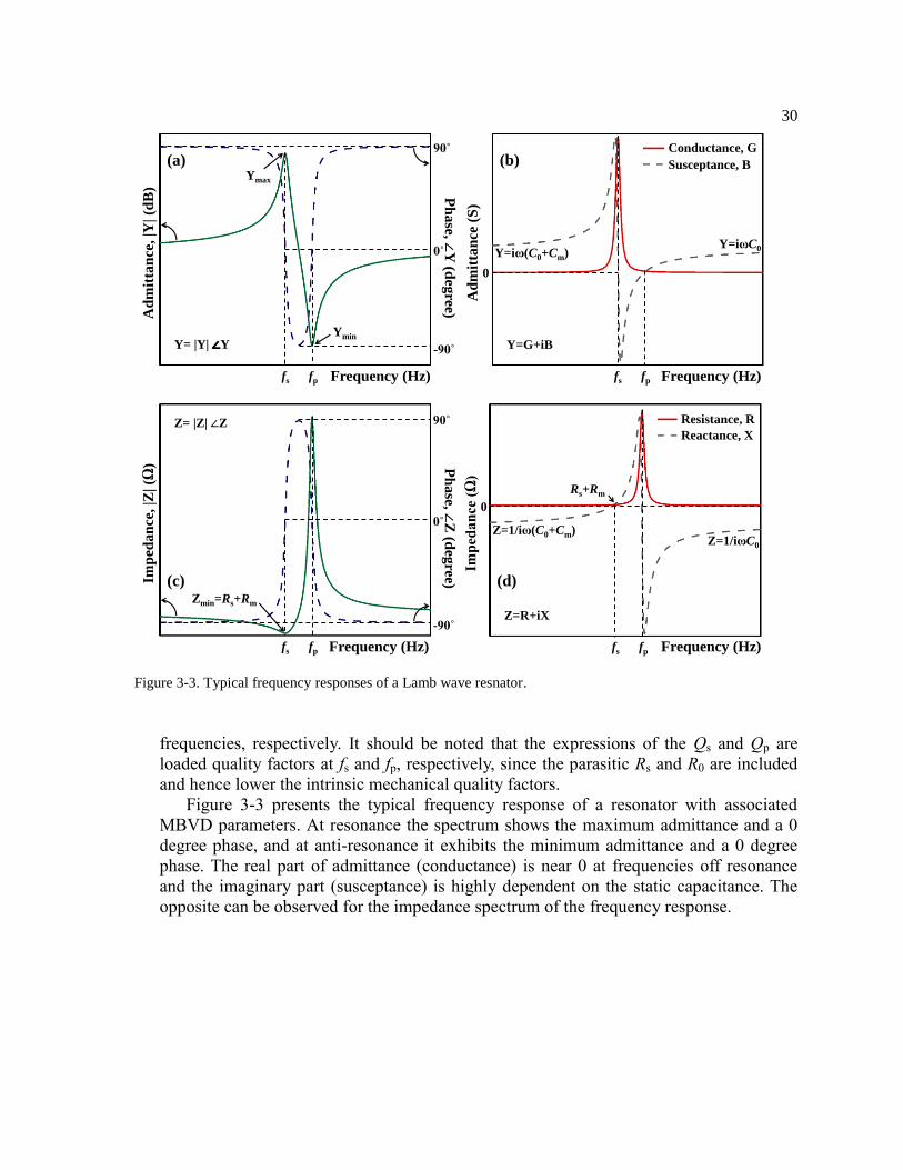
Figure 3-3 presents the typical frequency response of a resonator with associated
MBVD parameters. At resonance the spectrum shows the maximum admittance and a 0
degree phase, and at anti-resonance it exhibits the minimum admittance and a 0 degree
phase. The real part of admittance (conductance) is near 0 at frequencies off resonance
and the imaginary part (susceptance) is highly dependent on the static capacitance. The
opposite can be observed for the impedance spectrum of the frequency response.
Figure 3-3. Typical frequency responses of a Lamb wave resnator.
Frequency (Hz)
Ad
mit
tan
ce (
S)
fs fp
Conductance, G
0
Susceptance, B
Y=G+iB
Y=iω(C0+Cm)Y=iωC0
fs fp Frequency (Hz)
Imp
eda
nce
(Ω
)
Resistance, R
0
Reactance, X
Z=R+iX
Rs+Rm
Z=1/iω(C0+Cm)Z=1/iωC0
Frequency (Hz)
Imp
edan
ce,
|Z| (Ω
)
90˚
fs
-90˚
fp
0˚
Ph
ase,∠
Z (d
egree)
Zmin=Rs+Rm
Z= |Z| ∠Z
Frequency (Hz)
Ad
mit
tan
ce,
|Y| (d
B)
90˚
fs
-90˚
fp
0˚
Ph
ase,∠
Y (d
egree)
Y= |Y| ∠Y
Ymax
Ymin
(a) (b)
(c) (d)
31
3.2 The Effective Coupling Coefficient (k2
eff) Optimization
3.2.1 Electrode Configuration and AlN thicknesses
As introduced in the previous chapter, the intrinsic electromechanical coupling
coefficient k2 is a measure of the energy transduction efficiency between the electrical
and mechanical domains, and can be calculated by the velocity difference equation.
Nevertheless, the effective electromechanical coupling coefficient (keff2) for resonator
devices from the measured results can be evaluated in several ways, among which the
most often used definitions is IEEE standard definition.
𝑘𝑒𝑓𝑓2 =
𝜋
2
𝑓𝑠
𝑓𝑝[tan(
𝜋
2
𝑓𝑠
𝑓𝑝)]−1. (3.7)
The most used approximation for the effective coupling coefficient is
𝑘𝑒𝑓𝑓2 =
𝜋2
4(𝑓𝑝−𝑓𝑠
𝑓𝑝). (3.8)
The keff2 is in fully consistent with the k
2 for BAW resonators by this definition. But
for Lamb wave resonators there are small difference between these two measures. What’s
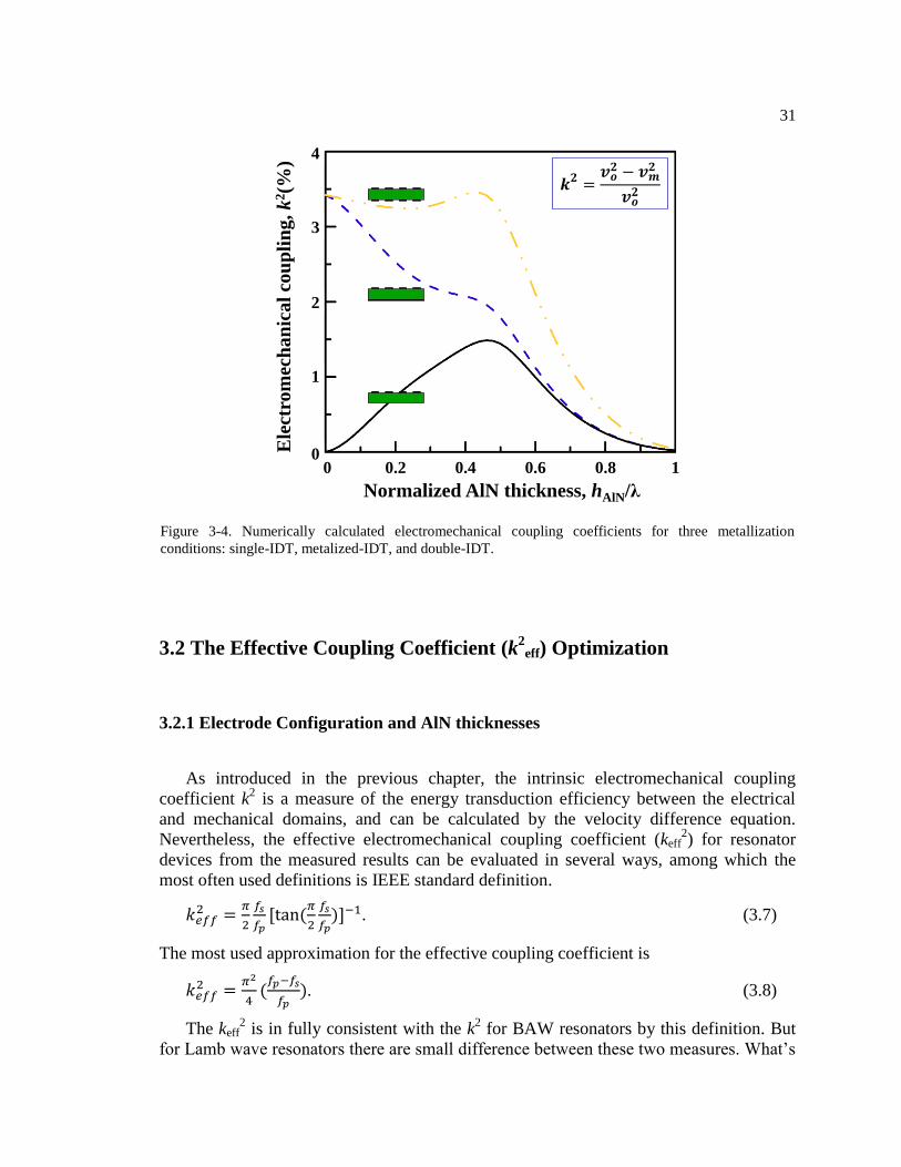
Figure 3-4. Numerically calculated electromechanical coupling coefficients for three metallization
conditions: single-IDT, metalized-IDT, and double-IDT.
00
2
0.2 0.4 0.6 0.8 1
Normalized AlN thickness, hAlN/λ
Ele
ctro
mec
han
ical
cou
pli
ng
, k
2(%
) 4
3
1
32
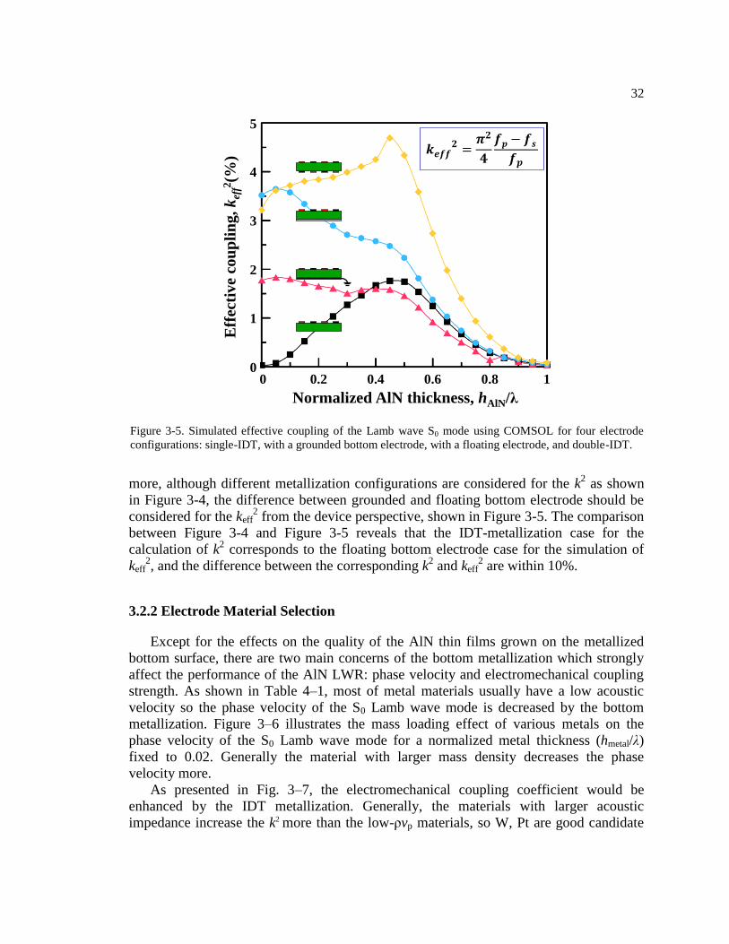
more, although different metallization configurations are considered for the k2 as shown
in Figure 3-4, the difference between grounded and floating bottom electrode should be
considered for the keff2 from the device perspective, shown in Figure 3-5. The comparison
between Figure 3-4 and Figure 3-5 reveals that the IDT-metallization case for the
calculation of k2 corresponds to the floating bottom electrode case for the simulation of
keff2, and the difference between the corresponding k
2 and keff
2 are within 10%.
3.2.2 Electrode Material Selection
Except for the effects on the quality of the AlN thin films grown on the metallized
bottom surface, there are two main concerns of the bottom metallization which strongly
affect the performance of the AlN LWR: phase velocity and electromechanical coupling
strength. As shown in Table 4–1, most of metal materials usually have a low acoustic
velocity so the phase velocity of the S0 Lamb wave mode is decreased by the bottom
metallization. Figure 3–6 illustrates the mass loading effect of various metals on the
phase velocity of the S0 Lamb wave mode for a normalized metal thickness (hmetal/λ)
fixed to 0.02. Generally the material with larger mass density decreases the phase
velocity more.
As presented in Fig. 3–7, the electromechanical coupling coefficient would be
enhanced by the IDT metallization. Generally, the materials with larger acoustic
impedance increase the k2 more than the low-ρvp materials, so W, Pt are good candidate
Figure 3-5. Simulated effective coupling of the Lamb wave S0 mode using COMSOL for four electrode
configurations: single-IDT, with a grounded bottom electrode, with a floating electrode, and double-IDT.
00
1
3
0.2 0.4 0.6 0.8 1
Normalized AlN thickness, hAlN/λ
Eff
ecti
ve
cou
pli
ng
, k
eff2
(%)
4
5
2
33
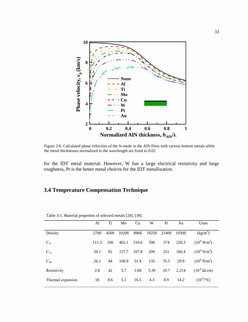
for the IDT metal material. However, W has a large electrical resistivity and large
roughness, Pt is the better metal choices for the IDT metallization.
3.4 Temperature Compensation Technique
Figure 3-6. Calculated phase velocities of the S0 mode in the AlN films with various bottom metals while
the metal thicknesses normalized to the wavelength are fixed to 0.02.
Table 3-1. Material properties of selected metals [28], [39].
Al Ti Mo Cu W Pt Au Units
Density 2700 4500 10200 8960 19250 21400 19300 (kg/m3)
C11 111.3 166 462.1 210.6 590 374 220.2 (109 N/m
2)
C12 59.1 92 157.7 107.8 200 251 160.4 (109 N/m
2)
C44 26.1 44 108.9 51.4 135 76.5 29.9 (109 N/m
2)
Resistivity 2.8 42 5.7 1.68 5.39 10.7 2.214 (10-6
Ω∙cm)
Thermal expansion 18 8.6 5.1 16.5 4.3 8.9 14.2 (10-6
/)
02
0.2 0.4 0.6 0.8 1
Normalized AlN thickness, hAlN/λ
8
6
4
10
Ph
ase
vel
oci
ty, v p
(km
/s)
Al
Mo
Ti
Cu
Pt
Au
W
None
34
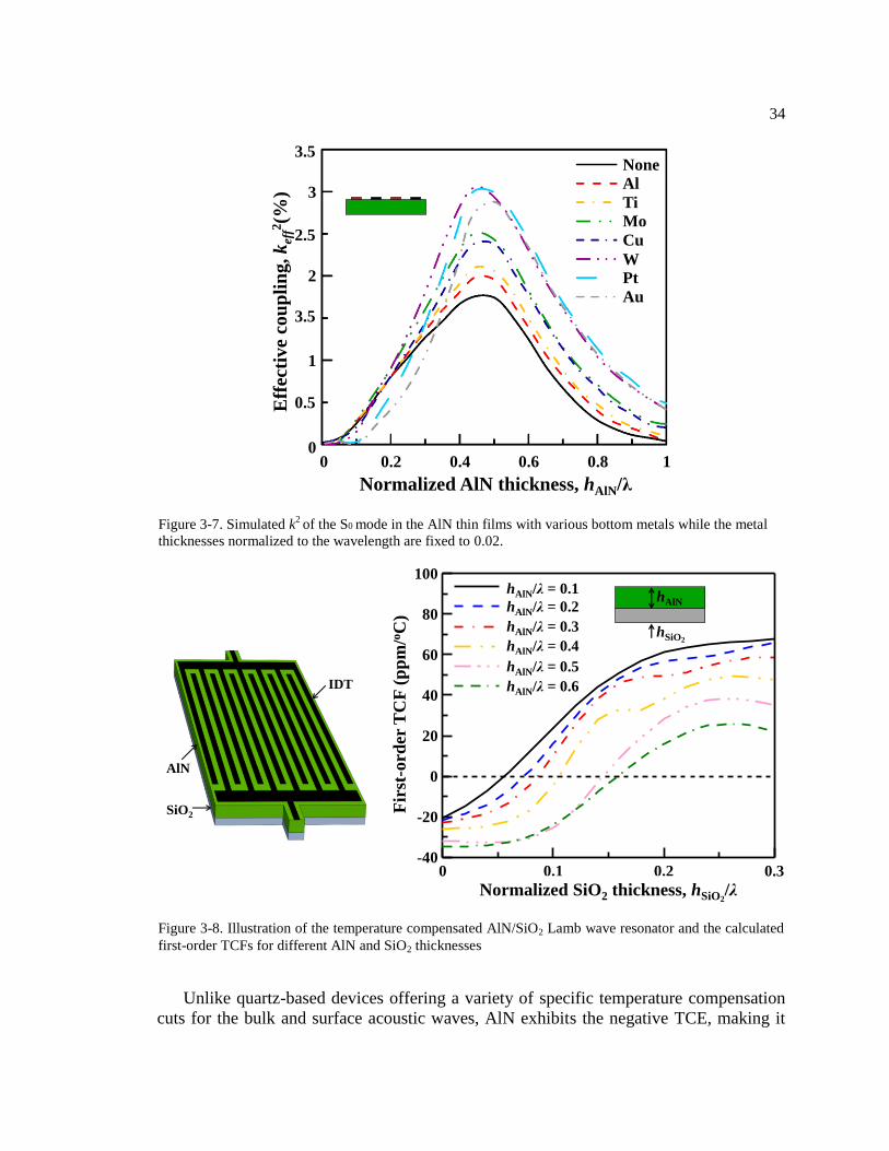
Unlike quartz-based devices offering a variety of specific temperature compensation
cuts for the bulk and surface acoustic waves, AlN exhibits the negative TCE, making it
Figure 3-8. Illustration of the temperature compensated AlN/SiO2 Lamb wave resonator and the calculated
first-order TCFs for different AlN and SiO2 thicknesses
Figure 3-7. Simulated k2 of the S0 mode in the AlN thin films with various bottom metals while the metal
thicknesses normalized to the wavelength are fixed to 0.02.
IDT
SiO2
AlN
0 0.1 0.2 0.3-40
-20
0
20
40
60
80
1000.1
0.2
0.3
0.4
0.5
0.6
hAlN/λ = 0.4
hAlN/λ = 0.6
hAlN/λ = 0.5
hAlN/λ = 0.3
hAlN/λ = 0.2
hAlN/λ = 0.1
Normalized SiO2 thickness, hSiO2/λ
Fir
st-o
rder
TC
F (
pp
m/o
C)
hAlN
hSiO2
00
1
0.2 0.4 0.6 0.8 1
Normalized AlN thickness, hAlN/λ
3
3.5
2
2.5
3.5
0.5Eff
ecti
ve
cou
pli
ng,
kef
f2(%
)
Al
Mo
Ti
Cu
Pt
Au
W
None
35
impossible to enable intrinsically temperature-compensated electroacoustic devices. The
temperature compensation of the AlN-based devices is therefore achieved by employing
thin film materials with opposite TCF. By adding a SiO2 layer with a TCF of 85 ppm/°C
onto the piezoelectric AlN layer, a robust temperature compensation approach for the
LWRs on an AlN/SiO2 bilayer plate has been successfully demonstrated at room
temperature and high temperatures.
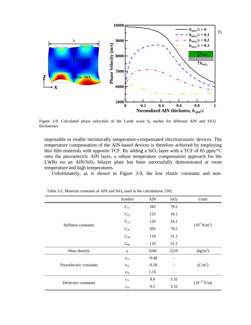
Unfortunately, as is shown in Figure 3-9, the low elastic constants and non-
Table 3-2. Material constants of AlN and SiO2 used in the calculations. [50]
Symbol AlN SiO2 Units
Stiffness constants
C11 345 78.5
(109 N/m
2)
C12 125 16.1
C13 120 16.1
C33 395 78.5
C44 118 31.2
C66 110 31.2
Mass density ρ 3260 2210 (kg/m3)
Piezoelectric constants
e15 –0.48 –
(C/m2) e31 –0.58 –
e33 1.55 –
Dielectric constants ε11 8.0 3.32
(10−11
F/m) ε33 9.5 3.32
Figure 3-9. Calculated phase velocities of the Lamb wave S0 modes for different AlN and SiO2
thicknesses.
x
z
0.5λ AlN
0.2λ SiO2
λ
0 0.2 0.4 0.6 0.8 15000
6000
7000
8000
9000
10000sio2=0
sio2=0.05
sio2=0.1
sio2=0.15
Normalized AlN thickness, hAlN/λP
ha
se V
elo
city
(m
/s)
hSiO2/λ = 0.3
hSiO2/λ = 0.2
hSiO2/λ = 0.1
hSiO2/λ = 0
hAlN
hSiO2
36
piezoelectricity of the SiO2 layer causes substantial reductions in the phase velocity and
electromechanical coupling coefficient. Furthermore, the asymmetrical composite plate
traps less acoustic waves in the AlN active layer so that the piezoelectric energy is
excited less efficiently to enable lower vp and smaller k2 for the S0 Lamb wave mode in
the AlN/SiO2 membrane. Figure 3-9 also shows the phase velocities for different AlN and
SiO2 thicknesses calculated using the material parameters listed in Figure 4-2. It is very
clear that the adding layer of SiO2 substantially lowers the phase velocity. When the
normalized SiO2 thickness reached 0.3, the phase velocity of the structure is almost
halved compared to the pure AlN membrane.
Because of the asymmetry in the z-axis direction, five different electrode
configurations should be considered for the analysis of electromechanical coupling, as is
listed in Figure 3-10, and the calculated electromechanical coupling from the material
properties in Table 3-2 for a mostly used SiO2 thickness - 0.2 - is also given in the figure.
It is obvious that the double-IDT configuration always exhibit the largest coupling, the
configurations when the IDTs are placed in the outer surface of AlN shows a larger
coupling when the normalized AlN thickness is around 0.55, and the configurations when
the IDTs are placed in the interface of AlN and SiO2 shows a larger coupling when the
normalized AlN thickness is around 0.05.
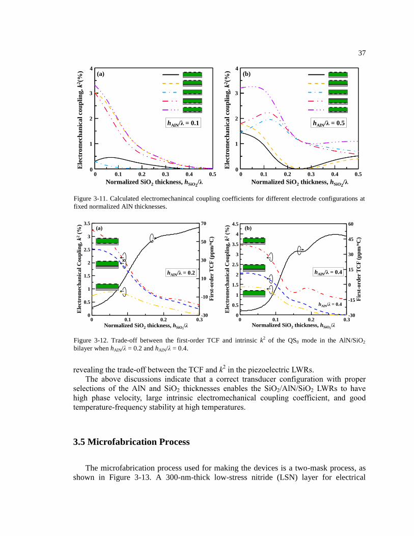
Figure 3-11 also compares the electromechanical coupling for different electrode
configurations but at fixed normalized AlN thicknesses, which indicate that for thin AlN
the bottom electrode is highly preferred and for thick AlN placing the IDT at the interface
can largely increase the k2.
Furthermore, the trade-off between the TCF and k2 can be observed in the same
propagation medium. As shown in Figure 3-12, when the k2 on the AlN/SiO2 composite
membrane achieve a locally minimum, it exhibits a locally maximal TCF, and vice versa,
Figure 3-10. Calculated electromechanical coupling coefficients of the QS0 mode for different electrode
configurations listed when hSiO2/λ=0.2.
hAlN
hSiO2
IDT
Configuration E
metallization
Configuration F
Configuration G Configuration H
Configuration I
00
0.8
0.2 0.4 0.6 0.8 1
Normalized AlN thickness, hAlN/λ
1.6
2
1.2
0.4
Ele
ctro
mec
ha
nic
al
cou
pli
ng
, k
2(%
)
hSiO2/λ = 0.2
37
revealing the trade-off between the TCF and k2 in the piezoelectric LWRs.
The above discussions indicate that a correct transducer configuration with proper
selections of the AlN and SiO2 thicknesses enables the SiO2/AlN/SiO2 LWRs to have
high phase velocity, large intrinsic electromechanical coupling coefficient, and good
temperature-frequency stability at high temperatures.
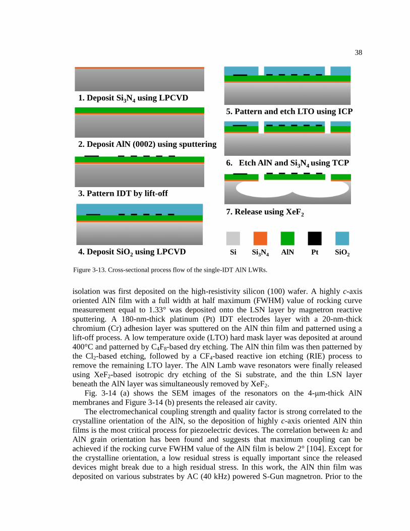
3.5 Microfabrication Process
The microfabrication process used for making the devices is a two-mask process, as
shown in Figure 3-13. A 300-nm-thick low-stress nitride (LSN) layer for electrical
Figure 3-11. Calculated electromechanincal coupling coefficients for different electrode configurations at
fixed normalized AlN thicknesses.
Figure 3-12. Trade-off between the first-order TCF and intrinsic k2 of the QS0 mode in the AlN/SiO2
bilayer when hAlN/λ = 0.2 and hAlN/λ = 0.4.
00
1
0.1 0.2 0.3 0.4 0.5
Normalized SiO2 thickness, hSiO2/λ
3
4
2
Ele
ctro
mec
ha
nic
al
cou
pli
ng
, k
2(%
)
hAlN/λ = 0.1
00
1
0.1 0.2 0.3 0.4 0.5
Normalized SiO2 thickness, hSiO2/λ
3
4
2
Ele
ctro
mec
ha
nic
al
cou
pli
ng
, k
2(%
)
hAlN/λ = 0.5
(a) (b)
hAlN/λ = 0.2
0 0.1 0.2 0.30
0.5
1
1.5
2
2.5
3
3.5
-30
-10
10
30
50
70
Normalized SiO2 thickness, hSiO2/λ
Ele
ctro
mec
han
ical
Cou
pli
ng
, k
2(%
)
Fir
st-o
rder
TC
F (
pp
m/o
C)
Ele
ctro
mec
han
ical
Cou
pli
ng
, k
2(%
)
Fir
st-o
rder
TC
F (
pp
m/o
C)
Normalized SiO2 thickness, hSiO2/λ
hAlN/λ = 0.4
0 0.1 0.2 0.30
0.5
1
1.5
2
2.5
3
3.5
4
4.5
-30
-15
0
15
30
45
60
hAlN/λ = 0.4
(a) (b)
38
isolation was first deposited on the high-resistivity silicon (100) wafer. A highly c-axis
oriented AlN film with a full width at half maximum (FWHM) value of rocking curve
measurement equal to 1.33° was deposited onto the LSN layer by magnetron reactive
sputtering. A 180-nm-thick platinum (Pt) IDT electrodes layer with a 20-nm-thick
chromium (Cr) adhesion layer was sputtered on the AlN thin film and patterned using a
lift-off process. A low temperature oxide (LTO) hard mask layer was deposited at around
400°C and patterned by C4F8-based dry etching. The AlN thin film was then patterned by
the Cl2-based etching, followed by a CF4-based reactive ion etching (RIE) process to
remove the remaining LTO layer. The AlN Lamb wave resonators were finally released
using XeF2-based isotropic dry etching of the Si substrate, and the thin LSN layer
beneath the AlN layer was simultaneously removed by XeF2.
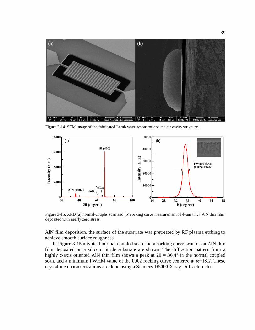
Fig. 3-14 (a) shows the SEM images of the resonators on the 4-μm-thick AlN
membranes and Figure 3-14 (b) presents the released air cavity.
The electromechanical coupling strength and quality factor is strong correlated to the
crystalline orientation of the AlN, so the deposition of highly c-axis oriented AlN thin
films is the most critical process for piezoelectric devices. The correlation between k2 and
AlN grain orientation has been found and suggests that maximum coupling can be
achieved if the rocking curve FWHM value of the AlN film is below 2° [104]. Except for
the crystalline orientation, a low residual stress is equally important since the released
devices might break due to a high residual stress. In this work, the AlN thin film was
deposited on various substrates by AC (40 kHz) powered S-Gun magnetron. Prior to the
Figure 3-13. Cross-sectional process flow of the single-IDT AlN LWRs.
1. Deposit Si3N4 using LPCVD
3. Pattern IDT by lift-off
4. Deposit SiO2 using LPCVD
2. Deposit AlN (0002) using sputtering
5. Pattern and etch LTO using ICP
7. Release using XeF2
6. Etch AlN and Si3N4 using TCP
SiO2Si Si3N4 AlN Pt
39
AlN film deposition, the surface of the substrate was pretreated by RF plasma etching to
achieve smooth surface roughness.
In Figure 3-15 a typical normal coupled scan and a rocking curve scan of an AlN thin
film deposited on a silicon nitride substrate are shown. The diffraction pattern from a
highly c-axis oriented AlN thin film shows a peak at 2θ = 36.4° in the normal coupled
scan, and a minimum FWHM value of the 0002 rocking curve centered at ω=18.2. These
crystalline characterizations are done using a Siemens D5000 X-ray Diffractometer.
Figure 3-14. SEM image of the fabricated Lamb wave resonator and the air cavity structure.
Figure 3-15. XRD (a) normal-couple scan and (b) rocking curve measurement of 4-μm thick AlN thin film
deposited with nearly zero stress.
(a) (b)
24 28 32 36 40 44 480
10000
20000
30000
40000
50000
θ (degree)
Inte
nsi
ty (
a. u
.)
FWHM of AlN
(0002)=0.9487°
Inte
nsi
ty (
a.
u.)
2θ (degree)
AlN (0002)
Si (400)
CuKβWLα
(a) (b)
40
Chapter 4
Q Enhancement of AlN Lamb Wave
Resonators Using Butterfly-shaped
Plates
The small-in-size and CMOS-compatible MEMS resonators are likely to be the
driving core of a new generation of electronic devices such as RF filters, sensors, and
timing references [51], [52]. Thanks to the high frequencies, low Rm, and capability of
multiple frequencies operation on a single chip, the AlN Lamb wave resonators utilizing
the S0 mode have attracted attention among various micromechanical resonator
technologies [53]–[57]. However, the AlN Lamb wave resonator usually shows a Q
below 2,000 due to complicated energy dissipation mechanisms, so an improvement in its
Q is highly desirable to further enable low-loss filters, high-sensitivity sensors, and low-
phase-noise oscillators.
3.1 Loss Mechanisms
Unlike the capacitive resonators that tend to show a very high Q but a huge Rm,
piezoelectric resonators usually exhibit a large coupling which leads a small Rm, but
unfortunately they show a medium Q [52], [58], [59]. Different loss mechanisms in
piezoelectric MEMS resonators have been investigated recently, and the interfacial loss,
causing from the stress jump at the material interface [62]–[64] as well as the anchor loss,
representing the acoustic energy leakage via the support tethers into the substrates [64]–
[71], are now suspected of the primary energy dissipation mechanisms. Fortunately, the
electrode-to-piezoelectric stress can be minimized with the optimized metal deposition
conditions [56] or separating the piezoelectric layer from its metal electrode [63] to
reduce the interfacial loss. By suppressing the acoustic wave leakage through the tethers,
the Q of the piezoelectric resonators can be improved [66]–[71].
Generally, the anchor loss of the MEMS resonators can be minimized by many
strategies, such as positioning the tethers at nodal locations of the resonance mode,
narrowing the width of the support tethers, using different materials for the support and
41
vibrating body to form an acoustic impedance mismatch, and designing the tether length
with an odd multiple of a quarter-wavelength (λ/4) [65]. Another effective way of
reducing the anchor loss is to reflect the acoustic waves leaky via the tethers back to the
resonant structure [67], [70], [71] or to concentrate the acoustic wave displacement far
from the supporting area [18]. Recently, the suspended biconvex edges were
demonstrated to efficiently concentrate the Lamb wave distributions in the resonance
plate and then boost the Q. However, some unwanted spurious vibration modes were also
introduced due to the curved reflecting edges [68].
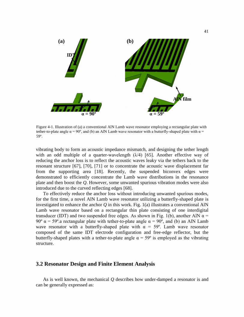
To effectively reduce the anchor loss without introducing unwanted spurious modes,
for the first time, a novel AlN Lamb wave resonator utilizing a butterfly-shaped plate is
investigated to enhance the anchor Q in this work. Fig. 1(a) illustrates a conventional AlN
Lamb wave resonator based on a rectangular thin plate consisting of one interdigital
transducer (IDT) and two suspended free edges. As shown in Fig. 1(b), another AlN α =
90º α = 59º.a rectangular plate with tether-to-plate angle α = 90º, and (b) an AlN Lamb
wave resonator with a butterfly-shaped plate with α = 59º. Lamb wave resonator
composed of the same IDT electrode configuration and free-edge reflector, but the
butterfly-shaped plates with a tether-to-plate angle α = 59º is employed as the vibrating
structure.
3.2 Resonator Design and Finite Element Analysis
As is well known, the mechanical Q describes how under-damped a resonator is and
can be generally expressed as:
Figure 4-1. Illustration of (a) a conventional AlN Lamb wave resonator employing a rectangular plate with
tether-to-plate angle α = 90º, and (b) an AlN Lamb wave resonator with a butterfly-shaped plate with α =
59º.
α = 90º α = 59º
AlN film
(a) (b)
IDT
42
stored
dissipated
2 ,E
QE
(4.1)
where Estored is the vibration energy stored in the resonator and Edissipated denotes the
energy dissipated per cycle of vibration, respectively. It is clear that to obtain a higher Q,
it requires more energy stored in the resonator and less energy dissipation, indicating that
the magnitude of Q ultimately depends on the energy loss in resonators. The most
relevant loss mechanisms in piezoelectric resonators are the anchor loss, interface loss,
thermoelastic damping (TED), material damping, and other unknown losses 60, 61. Then,
the total Q can be estimated by adding the impact of each specific energy loss
mechanism:
total anchor interface TED material unknown
1 1 1 1 1 1.
Q Q Q Q Q Q (4.2)
The interface loss, Qinterface, is caused by the plane stress jump at the material interface
and can be minimized by controlling the interfacial stresses during the deposition process.
The thermoelastic damping, QTED, means the energy dissipation during vibration which
produces a strain gradient, which leads to a temperature gradient, yielding the heat flow
as well as the energy loss. The material damping, Qmaterial, is related to the crystal defects
in the material, surface roughness, or grain size so it is difficult to estimate the Qmaterial. In
this work, we simply assume that the anchor loss, Qanchor, is the main energy dissipation
source in the resonator so we simplify the Qtotal is contributed by the Qanchor and other
losses, Qother, as following:
total anchor other
1 1 1.
Q Q Q
(4.3)
In this work, we propose a novel AlN plate geometry to reduce the tether vibration
caused by the resonant structure to increase the Qanchor. In order to study the effect of the
plate shape on Q, the Lamb wave resonators on AlN plates utilizing a rectangular plate
and a butterfly-shaped plate are designed and compared as summarized and listed in
Table 4-1: Geometric dimensions of the AlN Lamb wave resonators.
Conventional Butterfly-shaped
IDT finger electrode 13 13
IDT aperture 180 μm 180 μm
IDT electrode width 3 μm 3 μm
IDT electrode thickness 200 nm 200 nm
Tether-to-plate angle 90° 59°
Tether length 33 μm 33 μm
Tether width 8 μm 8 μm
AlN plate length 210 μm 252 μm
AlN plate width 78 μm 78 μm
AlN plate thickness 4.0 μm 4.0 μm
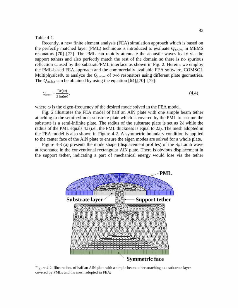
43
Table 4-1.
Recently, a new finite element analysis (FEA) simulation approach which is based on
the perfectly matched layer (PML) technique is introduced to evaluate Qanchor in MEMS
resonators [70]–[72]. The PML can rapidly attenuate the acoustic waves leaky via the
support tethers and also perfectly match the rest of the domain so there is no spurious
reflection caused by the substrate/PML interface as shown in Fig. 2. Herein, we employ
the PML-based FEA approach and the commercially available FEA software, COMSOL
Multiphysics®, to analyze the Qanchor of two resonators using different plate geometries.
The Qanchor can be obtained by using the equation [64],[70]–[72]:
anchor
Re( ),
2 Im( )Q
(4.4)
where ω is the eigen-frequency of the desired mode solved in the FEA model.
Fig. 2 illustrates the FEA model of half an AlN plate with one simple beam tether
attaching to the semi-cylinder substrate plate which is covered by the PML to assume the
substrate is a semi-infinite plate. The radius of the substrate plate is set as 2λ while the
radius of the PML equals 4λ (i.e., the PML thickness is equal to 2λ). The mesh adopted in
the FEA model is also shown in Figure 4-2. A symmetric boundary condition is applied
to the center face of the AlN plate to ensure the eigen modes are solved for a whole plate.
Figure 4-3 (a) presents the mode shape (displacement profiles) of the S0 Lamb wave
at resonance in the conventional rectangular AlN plate. There is obvious displacement in
the support tether, indicating a part of mechanical energy would lose via the tether
Figure 4-2. Illustrations of half an AlN plate with a simple beam tether attaching to a substrate layer
covered by PMLs and the mesh adopted in FEA.
PML
Symmetric face
Support tetherSubstrate layer
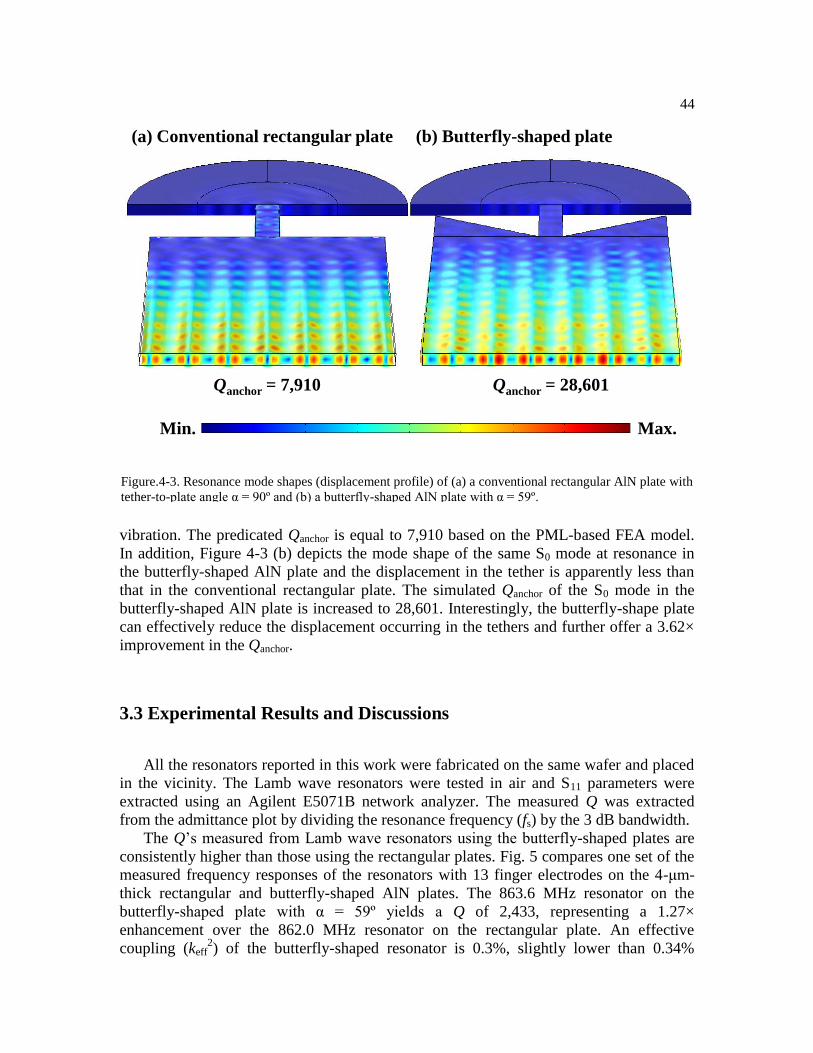
44
vibration. The predicated Qanchor is equal to 7,910 based on the PML-based FEA model.
In addition, Figure 4-3 (b) depicts the mode shape of the same S0 mode at resonance in
the butterfly-shaped AlN plate and the displacement in the tether is apparently less than
that in the conventional rectangular plate. The simulated Qanchor of the S0 mode in the
butterfly-shaped AlN plate is increased to 28,601. Interestingly, the butterfly-shape plate
can effectively reduce the displacement occurring in the tethers and further offer a 3.62×
improvement in the Qanchor.
3.3 Experimental Results and Discussions
All the resonators reported in this work were fabricated on the same wafer and placed
in the vicinity. The Lamb wave resonators were tested in air and S11 parameters were
extracted using an Agilent E5071B network analyzer. The measured Q was extracted
from the admittance plot by dividing the resonance frequency (fs) by the 3 dB bandwidth.
The Q’s measured from Lamb wave resonators using the butterfly-shaped plates are
consistently higher than those using the rectangular plates. Fig. 5 compares one set of the
measured frequency responses of the resonators with 13 finger electrodes on the 4-μm-
thick rectangular and butterfly-shaped AlN plates. The 863.6 MHz resonator on the
butterfly-shaped plate with α = 59º yields a Q of 2,433, representing a 1.27×
enhancement over the 862.0 MHz resonator on the rectangular plate. An effective
coupling (keff2) of the butterfly-shaped resonator is 0.3%, slightly lower than 0.34%
Figure.4-3. Resonance mode shapes (displacement profile) of (a) a conventional rectangular AlN plate with
tether-to-plate angle α = 90º and (b) a butterfly-shaped AlN plate with α = 59º.
Max.Min.
(a) Conventional rectangular plate (b) Butterfly-shaped plate
Qanchor = 7,910 Qanchor = 28,601
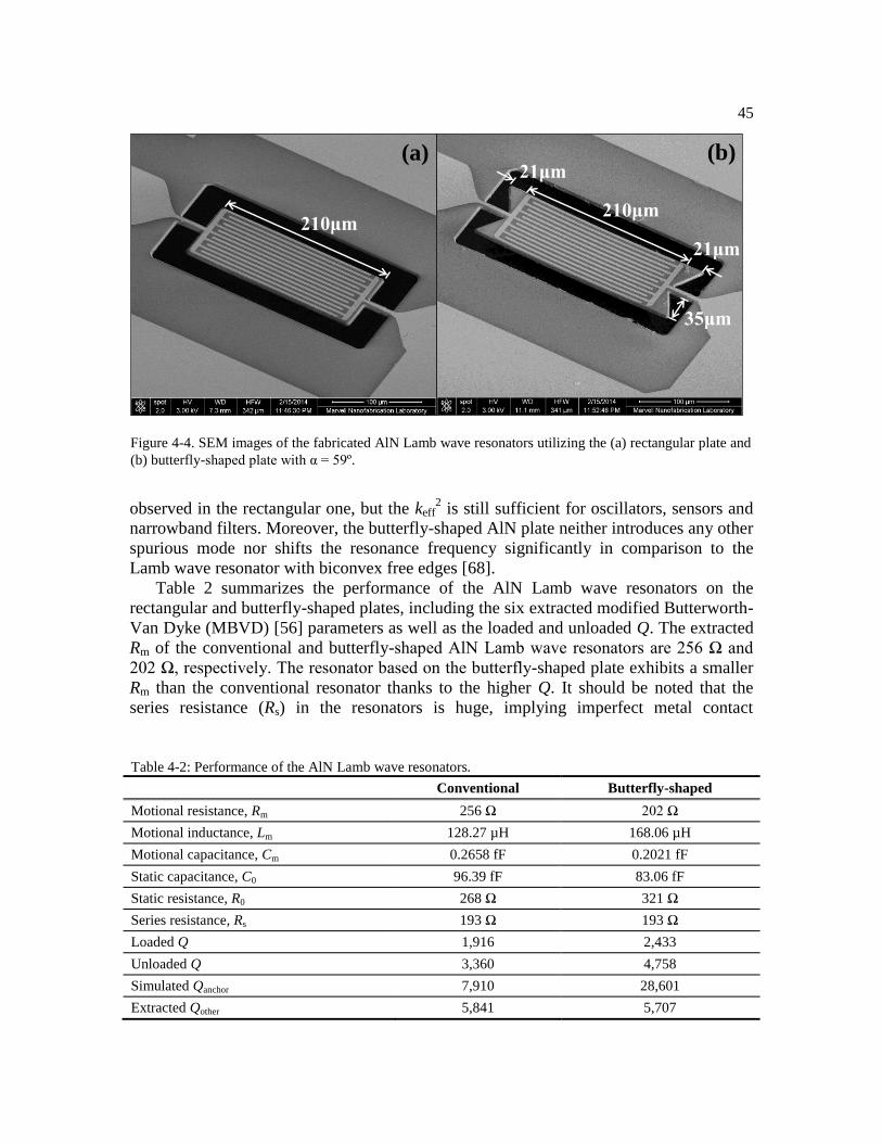
45
observed in the rectangular one, but the keff2 is still sufficient for oscillators, sensors and
narrowband filters. Moreover, the butterfly-shaped AlN plate neither introduces any other
spurious mode nor shifts the resonance frequency significantly in comparison to the
Lamb wave resonator with biconvex free edges [68].
Table 2 summarizes the performance of the AlN Lamb wave resonators on the
rectangular and butterfly-shaped plates, including the six extracted modified Butterworth-
Van Dyke (MBVD) [56] parameters as well as the loaded and unloaded Q. The extracted
Rm of the conventional and butterfly-shaped AlN Lamb wave resonators are 256 Ω and
202 Ω, respectively. The resonator based on the butterfly-shaped plate exhibits a smaller
Rm than the conventional resonator thanks to the higher Q. It should be noted that the
series resistance (Rs) in the resonators is huge, implying imperfect metal contact
Figure 4-4. SEM images of the fabricated AlN Lamb wave resonators utilizing the (a) rectangular plate and
(b) butterfly-shaped plate with α = 59º.
Table 4-2: Performance of the AlN Lamb wave resonators.
Conventional Butterfly-shaped
Motional resistance, Rm 256 Ω 202 Ω
Motional inductance, Lm 128.27 µH 168.06 µH
Motional capacitance, Cm 0.2658 fF 0.2021 fF
Static capacitance, C0 96.39 fF 83.06 fF
Static resistance, R0 268 Ω 321 Ω
Series resistance, Rs 193 Ω 193 Ω
Loaded Q 1,916 2,433
Unloaded Q 3,360 4,758
Simulated Qanchor 7,910 28,601
Extracted Qother 5,841 5,707
210μm210μm
21μm
21μm
35μm
(a) (b)
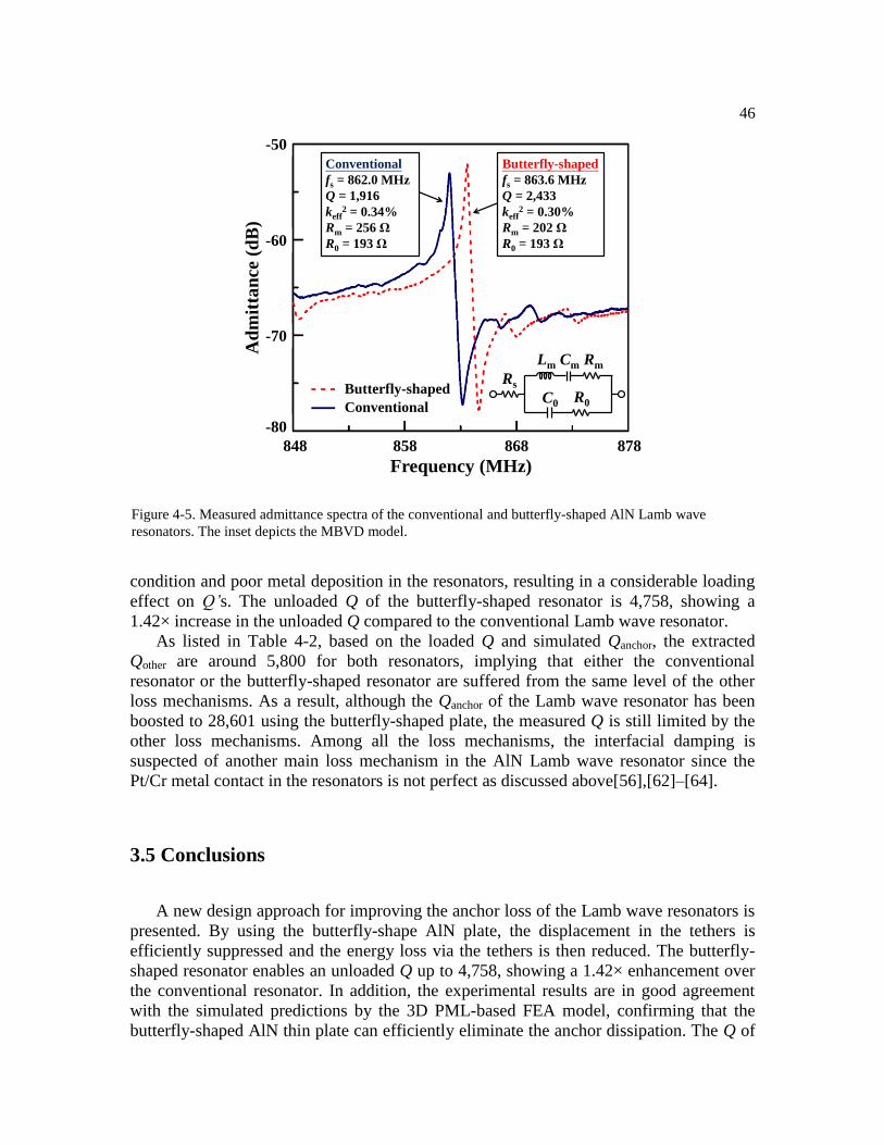
46
condition and poor metal deposition in the resonators, resulting in a considerable loading
effect on Q’s. The unloaded Q of the butterfly-shaped resonator is 4,758, showing a
1.42× increase in the unloaded Q compared to the conventional Lamb wave resonator.
As listed in Table 4-2, based on the loaded Q and simulated Qanchor, the extracted
Qother are around 5,800 for both resonators, implying that either the conventional
resonator or the butterfly-shaped resonator are suffered from the same level of the other
loss mechanisms. As a result, although the Qanchor of the Lamb wave resonator has been
boosted to 28,601 using the butterfly-shaped plate, the measured Q is still limited by the
other loss mechanisms. Among all the loss mechanisms, the interfacial damping is
suspected of another main loss mechanism in the AlN Lamb wave resonator since the
Pt/Cr metal contact in the resonators is not perfect as discussed above[56],[62]–[64].
3.5 Conclusions
A new design approach for improving the anchor loss of the Lamb wave resonators is
presented. By using the butterfly-shape AlN plate, the displacement in the tethers is
efficiently suppressed and the energy loss via the tethers is then reduced. The butterfly-
shaped resonator enables an unloaded Q up to 4,758, showing a 1.42× enhancement over
the conventional resonator. In addition, the experimental results are in good agreement
with the simulated predictions by the 3D PML-based FEA model, confirming that the
butterfly-shaped AlN thin plate can efficiently eliminate the anchor dissipation. The Q of
Figure 4-5. Measured admittance spectra of the conventional and butterfly-shaped AlN Lamb wave
resonators. The inset depicts the MBVD model.
Frequency (MHz)
Conventional
Butterfly-shaped
Butterfly-shaped
fs = 863.6 MHz
Q = 2,433
keff2 = 0.30%
Rm = 202 Ω
R0 = 193 Ω
Conventional
fs = 862.0 MHz
Q = 1,916
keff2 = 0.34%
Rm = 256 Ω
R0 = 193 Ω
-80
-70
-60
-50
848 858 868 878
RmCmLm
R0C0
Rs
Ad
mit
tan
ce (
dB
)
47
the Lamb wave resonators is expected to be significantly increased using the butterfly-
shaped plate if the interfacial loss can be minimized by well-controlled interface stresses
under optimized metal deposition conditions.
48
Chapter 5
Conclusions
The piezoelectric AlN LWRs present a promising resonator technology which offers
post-CMOS compatibility, multiple frequencies on a single chip, small size, low motional
impedance, medium keff2 and medium Q. The AlN LWRs show prospects to revolutionize
the current wireless communication systems, such as the application in the frequency
references or bandpass filters. Enjoying the merits of both SAW resonator and FBAR, the
low deposition temperature of the AlN thin film and the Si-based fabrication processes of
the LWRs show potential integration with the CMOS circuits, and the AlN LWRs can
offer multiple frequencies on one die for future realization of a single chip RF front-end.
Moreover, the LWRs present a superior in low motional resistances to the electrostatic
resonators, allowing interfacing with the standard 50 Ω RF systems. In order to enhance
the performance of the electronic system, the integration of micromechanical resonators
directly onto the circuitry is an excellent approach to avoid unnecessary energy loss.
However, the AlN Lamb wave resonator usually shows a Q below 2,000 due to
complicated energy dissipation mechanisms, so an improvement in its Q is highly
desirable to further enable low-loss filters, and low-phase-noise oscillators.
Different loss mechanisms in piezoelectric MEMS resonators have been investigated,
and the anchor loss, representing the acoustic energy leakage via the support tethers into
the substrates [14]–[21], are now suspected of the primary energy dissipation
mechanisms. By suppressing the acoustic wave leakage through the tethers, the Q of the
piezoelectric resonators can be improved. A new design approach for improving the
anchor loss of the Lamb wave resonators has been presented in this report. By using the
butterfly-shape AlN plate, the displacement in the tethers is efficiently suppressed and the
energy loss via the tethers is then reduced. The butterfly-shaped resonator enables an
unloaded Q up to 4,758, showing a 1.42× enhancement over the conventional resonator.
In addition, the experimental results are in good agreement with the simulated predictions
by the 3D PML-based FEA model.
49
Bibliography
1. C. T.-C. Nguyen, “MEMS technology for timing and frequency control,” IEEE
Trans. Ultrason. Ferroelectr. Freq. Control, vol. 54, pp. 251–270, Feb. 2007.
2. J. Wang, Z. Ren, and C. T.-C. Nguyen, “1.156-GHz self-aligned vibrating
micromechanical disk resonator,” IEEE Trans. Ultrason. Ferroelectr. Freq. Control,
vol. 51, pp. 1607–1628, Dec. 2004.
3. V. Yantchev and I. Katardjiev, “Micromachined thin film plate acoustic resonators
utilizing the lowest order symmetric Lamb wave mode,” IEEE Trans. Ultrason.
Ferroelectr. Freq. Control, vol. 54, pp. 87–95, Jan. 2007.
4. S. Gong, N.-K. Kuo, and G. Piazza, “GHz high-Q lateral overmoded bulk acoustic-
wave resonators using epitaxial SiC thin film,” J. Microelectromech. Syst., vol. 21,
pp. 253–255, Apr. 2012.
5. C.-M. Lin, Y.-Y. Chen, V. V. Felmetsger, D. G. Senesky, and A. P. Pisano,
“AlN/3C–SiC composite plate enabling high-frequency and high-Q micro-
mechanical resonators,” Adv. Mater., vol. 24, pp.2722–2727, May 2012.
6. V. Kaajakari, T. Mattila, A. Oja, J. Kiihamäki, and H. Seppä, “Square-extensional
mode single-crystal silicon micromechanical resonator for low-phase-noise
oscillator applications,” IEEE Electron Device Lett., vol. 25, pp.173–175, Apr. 2004.
7. Y.-W. Lin, S. Lee, S.-S. Li, Y. Xie, Z. Ren, and C. T.-C. Nguyen, “Series-resonant
VHF micromechanical resonator reference oscillators,” IEEE J. Solid-State Circuits,
vol. 39, pp.2477–2491, Dec. 2004.
8. C. Zuo, J. Van der Spiegel, and G. Piazza, “1.05-GHz CMOS oscillator based on
lateral-field-excited piezoelectric AlN contour-mode MEMS resonators,” IEEE
Trans. Ultrason. Ferroelectr. Freq. Control, vol. 57, pp. 82–87, Jan. 2010.
9. M. Rinaldi, C. Zuo, J. Van der Spiegel, and G. Piazza, “Reconfigurable CMOS
oscillator based on multi-frequency AlN contour-mode resonators,” IEEE Trans.
Electron Devices, vol. 58, pp. 1281–1286, May 2010.
10. W. Pang, R. C. Ruby, R. Parker, P. W. Fisher, M. A. Unkrich, and J. D. Larson, III,
“A temperature-stable film bulk acoustic wave oscillator,” IEEE Electron Device
Lett., vol. 20, pp.315–318, Apr. 2008.
11. R. C. Ruby, M. Small, F. Bi, D. Lee, L. Callaghan, R. Parker, and S. Ortiz,
“Positioning FBAR technology in the frequency and timing domain,” IEEE Trans.
Ultrason. Ferroelectr. Freq. Control, vol. 59, pp. 334–345, Mar. 2012.
12. M. A. Schmidt and R. T. Howe, “Silicon resonant microsensors,” Ceram. Eng. Sci.
Proc., vol. 8, pp. 1019–1034, Oct. 1987.
50
13. W. C. Tang, T.-C. H. Nguyen, and R. T. Howe, “Laterally driven polysilicon
resonant microstructures,” Sens. Actuators, vol. 20, pp. 25–32, Nov. 1989.
14. C. T.-C. Nguyen and R. T. Howe, “An integrated CMOS micromechanical resonator
high-Q oscillator,” IEEE J. Solid-State Circuits, vol. 34, pp.440–455, Apr. 1999.
15. J. R. Clark, W.-T. Hsu, and C. T.-C. Nguyen, “High-Q VHF micromechanical
contour-mode disk resonators,” in Tech. Dig. IEEE Intl. Electron Devices Mtg.,
2000, pp. 493–496.
16. J. R. Clark, W.-T. Hsu, M. A. Abdelmoneum, and C. T.-C. Nguyen, “High-Q UHF
micromechanical radial-contour mode disk resonators,” J. Microelectromech. Syst.,
vol. 14, pp. 1298–1310, Dec. 2005.
17. A. Ballato, “Piezoelectricity: history and new thrusts,” in Proc. IEEE Intl. Ultrason.
Symp., 1996, pp. 575–583.
18. B. Drafts, “Acoustic wave technology sensors,” IEEE Trans. Microw. Theory Tech.,
vol. 49, pp. 795–802, Apr. 2001.
19. L. Rayleigh, “On waves propagated along the plane surface on an elastic solid,”
Proc. London Math. Soc., vol. 17, pp. 4–11, Nov. 1885.
20. R. M. White and F. W. Voltmer, “Direct piezoelectric coupling to surface elastic
waves,” Appl. Phys. Lett., vol. 7, pp. 314–316, Dec. 1965.
21. R. Weigel, D. P. Morgan, J. M. Owens, A. Ballato, K. M. Lakin, K. Hashimoto, and
C. C. W. Ruppel, “Microwave acoustic materials, devices, and applications,” IEEE
Trans. Microw. Theory Tech., vol. 50, pp. 738–749, Mar. 2002.
22. M. Werner, S. Klose, F. Szücs, Ch. Moelle, H. J. Fecht, C. Johnston, P. R. Chalker,
and I. M. Buckley-Golder “High temperature Young's modulus of polycrystalline
diamond,” Diam. Relat. Mater., vol. 6, pp. 344–347, Mar. 1997.
23. T.-T. Wu and Y.-Y. Chen, “Exact analysis of dispersive SAW devices on
ZnO/diamond/Si layered structures,” IEEE Trans. Ultrason. Ferroelect. Freq.
Control, vol. 49, pp. 142–149, Jan. 2002.
24. M. El Hakiki, O. Elmazria, M. B. Assouar, V. Mortet, L. Le Brizoual, M. Vanecek,
and P. Alnot “ZnO/AlN/diamond layered structure for SAW devices combining high
velocity and high electromechanical coupling coefficient,” Diam. Relat. Mater., vol.
14, pp. 1175–1178, Mar.–Jul. 2005.
25. M. Benetti, D. Cannata, F. Di Pietrantonio, and E. Verona, “Growth of AlN
piezoelectric film on diamond for high-frequency surface acoustic wave devices,”
IEEE Trans. Ultrason. Ferroelectr. Freq. Control, vol. 52, pp. 1806–1811, Oct. 2005.
26. C.-M. Lin, T.-T. Wu, Y.-Y. Chen, and T.-T. Chou, “Improved frequency responses
of SAW filters with interdigitated interdigital transducers on ZnO/Diamond/Si
layered structure,” J. Mech. vol. 23, pp. 253–259, Sept. 2007.
27. K. Hashimoto, Ed., RF Bulk Acoustic Wave Filters for Communications, Norwood:
Artech House, 2009.
51
28. W. H. Horton and R. C. Smythe, “On the trapped-wave criterion for AT-cut quartz
resonators with coated electrodes,” Proc. IEEE, pp. 598–599, Apr. 1967.
29. K. M. Lakin, G. R. Kline and K. T. McCarron, “High-Q microwave acoustic
resonators and filters,” IEEE Trans. Microw. Theory Tech., vol. 41, pp. 2139–2146,
Dec. 1993.
30. W. E. Newell, “Face-mounted piezoelectric resonators,” Proc. IEEE, pp. 575–581,
Jun. 1965.
31. E. Klier, “Fundamental extensional mode of circular quartz plates,” Czech. J. Phys.,
vol. 3, pp. 72–82, Mar. 1953.
32. J. Hermann and C. Bourgeois, “A new quartz crystal cut for contour mode
resonators,” in Proc. IEEE Intl. Freq. Control Symp., 1979, pp. 255–262.
33. S. C. Hight and G. W. Willard, “A simplified circuit for frequency substandards
employing a new type of low-frequency zero-temperature-coefficient quartz crystal,”
Proc. Inst. Radio Eng., vol. 25, pp. 549–563, May 1937.
34. J.D. Larson, P. D. Bradley, S. Wartenberg, and R. C. Ruby,” Modified Butterworth-
Van Dyke circuit model for FBAR resonators and automated measurement system,”
n Proc. IEEE Int. Ultrason. Symp., Oct. 2000, pp. 863–868.
35. G. Piazza and A. P. Pisano, “Dry-released post-CMOS compatible contour-mode
aluminum nitride micromechanical resonators for VHF applications,” in Tech. Dig.
Solid-State Sens. Actuators Microsyst. Workshop, 2004, pp. 37–40.
36. G. Piazza, P. J. Stephanou, and A. P. Pisano, “Piezoelectric aluminum nitride
vibrating contour-mode MEMS resonators,” J. Microelectromech. Syst., vol. 15, pp.
1406–1418, Dec. 2006.
37. G. Piazza, P. J. Stephanou, and A. P. Pisano, “Single-chip multiple-frequency AlN
MEMS filters based on contour-mode piezoelectric resonators,” J. Microelectromech.
Syst., vol. 16, pp. 319–328, Apr. 2007.
38. K. Toda, “Lamb-wave delay lines with interdigital electrodes,” J. Appl. Phys., vol.
44, pp. 56–62, Jan. 1973.
39. A. J. Slobodnik Jr., E. D. Conway1 and R. T. Delmonico, “Microwave Acoustics
Handbook,” J. Acoust. Soc. Am., vol. 56, 1307, 1974.
40. R. M. White and S. W. Wenzel, “Fluid loading of a Lamb wave sensor,” Appl. Phys.
Lett., vol. 52, pp. 1653–1655, May 1988.
41. J. Bjurström, I. Katardjiev, and V. Yantchev, “Lateral-field-excited thin-film Lamb
wave resonator,” Appl. Phys. Lett., vol. 86, 154103, Apr. 2005.
42. J. Bjurström, I. Katardjiev, and V. Yantchev, “Thin film Lamb wave resonant
structure – the first approach,” Solid-State Electron., vol. 50, pp. 322–326, Mar. 2006.
43. V. Yantchev, and I. Katardjiev, “Micromachined thin film plate acoustic resonators
utilizing the lowest order symmetric Lamb wave mode,” IEEE Trans. Ultrason.
Ferroelect. Freq. Control, vol. 54, pp. 87–95, Jan. 2007.
52
44. V. Yantchev, L. Arapan, and I. Katardjiev, “Micromachined thin film plate acoustic
resonators (FPAR): Part II,” IEEE Trans. Ultrason. Ferroelect. Freq. Control, vol.
56, pp. 2701–2710, Dec. 2009.
45. P. J. Stephanou and A. P. Pisano, “800 MHz low motional resistance contour-
extensional aluminum nitride micromechanical resonators,” in Tech. Dig. Solid-State
Sens. Actuators Microsyst. Workshop, 2006, pp. 60–61.
46. G. Piazza, P. J. Stephanou, and A. P. Pisano, “One and two port piezoelectric higher
order contour-mode MEMS resonators for mechanical signal processing,” Solid-
State Electron., vol. 51, pp. 1596–1608, 2007.
47. M. Rinaldi, C. Zuniga, C. Zuo, and G. Piazza, “Super-high-frequency two-port AlN
contour-mode resonators for RF applications,” IEEE Trans. Ultrason. Ferroelect.
Freq. Control, vol. 57, pp. 38–45, Jan. 2010.
48. C. Zuo, N. Sinha, J. Van der Spiegel, and G. Piazza, “Multifrequency Pierce
oscillator based on piezoelectric AlN contour-mode MEMS technology,” J.
Microelectromech. Syst., vol. 19, pp. 570–580, Jun. 2010.
49. C.-M. Lin, Y.-J. Lai, T.-T. Yen, J.-C. Hsu, Y.-Y. Chen, D. G. Senesky, and A. P.
Pisano, “Quality factor enhancement in Lamb wave resonators utilizing AlN plates
with convex edges,” in Tech. Dig. Intl. Conf. Solid-State Sens. Actuators Microsyst.,
2011, pp. 1512–1515.
50. J. Bjurström, G. Wingqvist, V. Yantchev and I. Katardjiev, J. Micromech. Microeng,
17, 651 (2007).
51. C. T.-C. Nguyen, “MEMS technology for timing and frequency con- trol,” IEEE
Trans. Ultrason. Ferroelect. Freq. Control, vol. 54, pp. 251–270, Feb. 2007.
52. V. Yantchev and I. Katardjiev, “Thin film Lamb wave resonators in frequency
control and sensing applications: a review,” J. Micromech. Microeng., vol. 23,
043001, Apr. 2013.
53. G. Piazza, P.J. Stephanou, A.P. Pisano, “Piezoelectric Aluminum nitride vibrating
contour-mode MEMS resonators,” J. Microelectromech. Syst., vol. 15, pp. 1406–
1418, Dec. 2006.
54. C.-M. Lin, T.-T. Yen, Y.-J. Lai, V. V. Felmetsger, M. A. Hopcroft, J. H. Kuypers,
and A. P. Pisano, “Temperature-compensated aluminum nitride Lamb wave
resonators,” IEEE Trans. Ultrason. Ferroelectr. Freq. Control, vol. 57, pp. 524–
532, Mar. 2010
55. C.-M. Lin, T.-T. Yen, V. V. Felmetsger, M. A. Hopcroft, J. H. Kuypers, and A. P.
Pisano, “Thermally compensated aluminum nitride Lamb wave resonators for high
temperature applications,” Appl. Phys. Lett., vol. 97, 083501, Aug. 2010.
56. C.-M. Lin, V. Yantchev, J. Zou, Y.-Y. Chen, and A. P. Pisano, “Micromachined
one-port aluminum nitride Lamb wave resonators utilizing the lowest-order
symmetric mode,” J. Microelectromech. Syst., vol. 23, pp. 78–91, Feb. 2014.
57. J. Zou, C.-M. Lin, Y.-Y. Chen, and A. P. Pisano, “Theoretical study of thermally
stable SiO2/AlN/SiO2 Lamb wave resonators at high temperatures,” J. Appl. Phys.,
vol. 115, 094510, Mar. 2014.
53
58. C.-M. Lin , Y.-Y. Chen , V. V. Felmetsger, D. G. Senesky, and A. P. Pisano,
“AlN/3C–SiC composite plate enabling high-frequency and high-Q
micromechanical esonators,” Adv. Mater., vol. 24, pp. 2722–2727, May 2012.
59. C.-M. Lin, Y.-Y. Chen, and A. P. Pisano, “Theoretical investigation of Lamb wave
characteristics in AlN/3C–SiC composite membranes,” Appl. Phys. Lett., vol. 97,
193506, Nov. 2010.
60. W.-C. Li, Y. Lin, B. Kim, Z. Ren, and C. T.-C. Nguyen, “Quality factor
enhancement in micromechanical resonators at cryogenic temperatures,” in Proc.
Int. Conf. Solid-State Sens. Actuators Microsyst., Denvor, CO, Jun. 2009, pp. 1445–
1448.
61. S. Ghaffari, S. A. Chandorkar, S. Wang, E. J. Ng, C. H. Ahn, V. Hong, Y. Yang, and
T. W. Kenny, “Quantum limit of quality factor in silicon micro and nano mechanical
resonators,” Sci. Rep., vol. 3, 3244, Nov. 2013.
62. Z. Hao and B. Liao, “An analytical study on interfacial dissipation in piezoelectric
rectangular block resonators with in-plane longitudinal-mode vibrations,” Sens.
Actuators A: Phys., vol. 163, pp.401–409, Sept. 2010.
63. T.-T. Yen, A. P. Pisano, and C. T.-C. Nguyen, “High-Q capacitive-piezoelectric AlN
Lamb wave resonators,” in Proc. IEEE Int. Conf. Micro Electro Mech. Syst., Taipei,
Taiwan, Jan. 2013, pp. 114–117.
64. A. Frangia, M. Cremonesia, A. Jaakkolab, and T. Pensala, “Analysis of anchor and
interface losses in piezoelectric MEMS resonators,” Sens. Actuators A: Phys., vol.
190, pp.127–135, Feb. 2013.
65. L. Wu, M. Akgul, Z. Ren, Y. Lin, W.-C. Li, and C. T.-C. Nguyen, “Hollow stems
for higher micromechanical disk resonator quality factor”, in Proc. IEEE Intl.
Ultrason. Symp., Orlando, FL, Oct. 2011, pp. 1964–1967.
66. W. Pang, H. Zhang, S. Whangbo, and E.S. Kim, “High Q film bulk acoustic
resonator from 2.4 to 5.1 GHz,” in Proc. IEEE Int. Conf. Micro Electro Mech. Syst.,
Maastricht, Netherlands, Jan. 2004, pp. 805–808.
67. B. P. Harrington and R. Abdolvand, “In-plane acoustic reflectors for reducing
effective anchor loss in lateral-extensional MEMS resonators,” J. Micromech.
Microeng., vol. 21, 085021, Aug. 2011.
68. C.-M. Lin, Y.-J. Lai, J.-C. Hsu, Y.-Y. Chen, D. G. Senesky, and A. P. Pisano,
“High-Q aluminum nitride Lamb wave resonators with biconvex edges,” Appl. Phys.
Lett., vol. 99, 143501, Oct. 2011.
69. Y.-Y. Chen, Y.-T. Lai, and C.-M. Lin, “Finite element analysis of anchor loss in
AlN Lamb wave resonators,” in Proc. IEEE Int. Freq. Contr. Symp., Taipei, Taiwan,
2014, pp. 132–136.
70. C. Cassella, J. S. Fernandez, M. Cremonesi, A. Frangi, and G. Piazza, “Reduction of
anchor losses by etched slots in aluminum nitride contour mode resonators,” in Proc.
Eur. Freq. Time Forum & IEEE Int. Freq. Contr. Symp., Prague, Czech, 2013, pp.
926–929.
71. C.-M. Lin, J.-C. Hsu, D. G. Senesky, and A. P. Pisano, “Anchor loss reduction in
AlN Lamb wave resonators using phononic crystal strip tethers”, in Proc. IEEE Int.
Freq. Contr. Symp., Taipei, Taiwan, 2014, pp. 371–375.
54
72. D. S. Bindel and S. Govindjee, “Elastic PMLs for resonator anchor loss simulation,”
Int. J. Numer. Meth. Engng., vol. 64, pp. 798–818, Oct. 2005.