Embed Size (px)
Citation preview

High Sensitivity Signatures for Test and Diagnosis of Analog, Mixed-Signal andRadio-Frequency Circuits
by
Suraj Sindia
A dissertation submitted to the Graduate Faculty ofAuburn University
in partial fulfillment of therequirements for the Degree of
Doctor of Philosophy
Auburn, AlabamaAugust 3, 2013
Keywords: Analog Circuit, Test, Diagnosis, Mixed-Signal Test, Radio-Frequency Test,Signature-Based Test
Copyright 2013 by Suraj Sindia
Approved by
Vishwani D. Agrawal, Chair, James J. Danaher Professor of Electrical & Computer Eng.Foster F. Dai, Professor of Electrical & Computer Engineering
Adit D. Singh, James B. Davis Professor of Electrical & Computer EngineeringAlvin Lim, Professor of Computer Science & Software Engineering

Abstract
The conventional approach, widely practiced in the industry today, for testing analog
circuits is to ensure that the circuit conforms to data-sheet limits on all its specifications.
However, such a specification based test methodology suffers from high levels of test cost
stemming from long test-times on expensive test equipment. In recent years the situation
has only worsened with the advent of mixed signal systems on chip (SoC), to a point where
analog circuit test cost is often found to be as much as 50% of the total test cost in spite of
analog portions occupying less than 5% of the chip area.
To alleviate the analog circuit test cost problem, a number of techniques exist in the
literature that can be broadly classified as (a) fault-model based test or (b) alternate test.
Fault model based test techniques direct their tests to identify faults in circuit components
much like their digital circuit test counterparts resulting in a test approach that can be
easily automated and relies on readily available output measurements on inexpensive test
equipment. On the other hand, alternate test techniques test a circuit by building a regression
model relating a few easily observable output parameters as signatures of the circuit to the
actual circuit specification.
Both these test paradigms for analog circuit test, however, have limited industry accep-
tance due to a lack of confidence in the defect level and yield loss that the test procedures
can guarantee in the face of high manufacturing process variation and low signal levels that
are characteristic of modern analog circuits. An important reason for the (typically) high
defect level and yield loss resulting from the use of either of these two test paradigms is the
unavailability of easily obtainable circuit outputs that are (a) sufficiently sensitive to circuit
component values and (b) have a high degree of correlation with circuit specifications.
ii

The main objective of this thesis is to design analog test signatures (and associated
test procedures) that are (i) sensitive enough to capture even small variations in circuit
components, and (ii) sufficiently correlated to circuit specifications and yet obtainable at
limited or no additional hardware and input signal design effort. Additional objectives of this
thesis are to: 1) Extend the use of the new signatures to diagnose faulty circuit components
in analog circuits. 2) Use the test signatures to distinguish faults resulting from defects
caused by manufacturing process related variations. 3) Evaluate the theoretical bounds on
the achievable defect level and the resulting yield loss of fault model based test procedures
relying on these signatures.
The sensitivity of the proposed test signatures is enhanced by an exponential transforma-
tion, called V-Transform. The new test signatures and associated procedures are evaluated
using three metrics test time, defect level (test escapes), and yield loss. We analyze the
proposed signatures theoretically in addition to extensive computer simulations and hard-
ware measurements on common RF/analog circuits such as filters and low noise amplifiers.
A representative result of one of our experiments is as follows: For 400 low noise amplifier
circuits that were tested, we find that the proposed V-transform based signatures resulted
in smaller test escape (≈ 2%) and yield loss (≈ 3%) when compared to other prevailing
alternate test or fault-model based test methods, while significantly reducing test time (by
as much as 50%) compared to the traditional specification based test methods.
iii

Acknowledgments
First and foremost, I would like to thank my advisor Prof. Vishwani D. Agrawal for
encouraging me to start on this doctoral program and constantly challenging me to push the
limits and seek out bold, new ideas. His enthusiasm for research and learning is infectious,
which is something I hope I have picked up and would like to embody in my own life.
Big thanks goes out to Prof. Adit Singh and Prof. Foster Dai for serving on my thesis
committee, and in each of whose classes, I learned significant material that helped me get a
good grounding in the broad areas of VLSI Design and Test. Thanks are due to Prof. Alvin
Lim for serving as the external reader on my committee. I owe a debt of gratitude to Prof.
Virendra Singh (IIT Bombay, India), whose early interest in my work spurred me to pursue
it further, which has eventually come to be my PhD thesis. I should thank members of the
analog test community, particularly Haralampos Stratigopoulos (TIMA labs, France), whose
comments at various points in time have benefited this work.
Some other professors who I have interacted with closely and learned from are: Prof.
Prathima Agrawal through the Wireless Networking seminar series in which I presented at
least once and was educated on numerous emerging topics in wireless communication; Prof.
Stan Reeves, whose course on digital image processing helped spawn several of my papers
in the area of fault tolerant image processing; Prof. Stu Wentworth who offered the Radar
Engineering course where he helped us build a radar target model, but in him I saw first-hand
how to be a great teacher with a keen interest in the student success.
A word of thanks goes to all my present and past lab colleagues and office mates at
Auburn University for making it a fun place to spend long hours each day. Office staff in ECE,
namely Mary Lloyd, Shelia Collis and Linda Allgood were particularly helpful throughout
iv

my stay in Auburn. Linda Barresi and Joe Haggerty were helpful in procuring components
for my experiments in a timely fashion.
I acknowledge the Department of ECE at Auburn University for supporting my studies
with generous teaching fellowships; Auburn University Wireless Engineering Research and
Education Center (WEREC) for funding several conference travels. I would like to acknowl-
edge Intel Corporation, and my colleagues there, for being particularly supportive of my
thesis-writing effort during the last semester of my graduate school that I spent in practical
training.
Finally, I would like to thank my extended family for being supportive of all my endeav-
ors. This thesis is dedicated to them.
v

Poem by the Author
Working is tricky,
If you choose to be picky!
Research is sucky,
When you try to be finicky!
I knew this already,
But I chose to be heady.
After a while,
I’ve realized, it was all worthwhile!
I pushed myself to publish many papers,
Even as I wonder if they’ll end up in diapers!
I hope many other folks will cite my paper,
Lest I be labeled an academic pauper!
I’m finishing this dissertation,
Without much adoration;
Oh God, my Committee,
Will they approve my Ph.D.?
vi
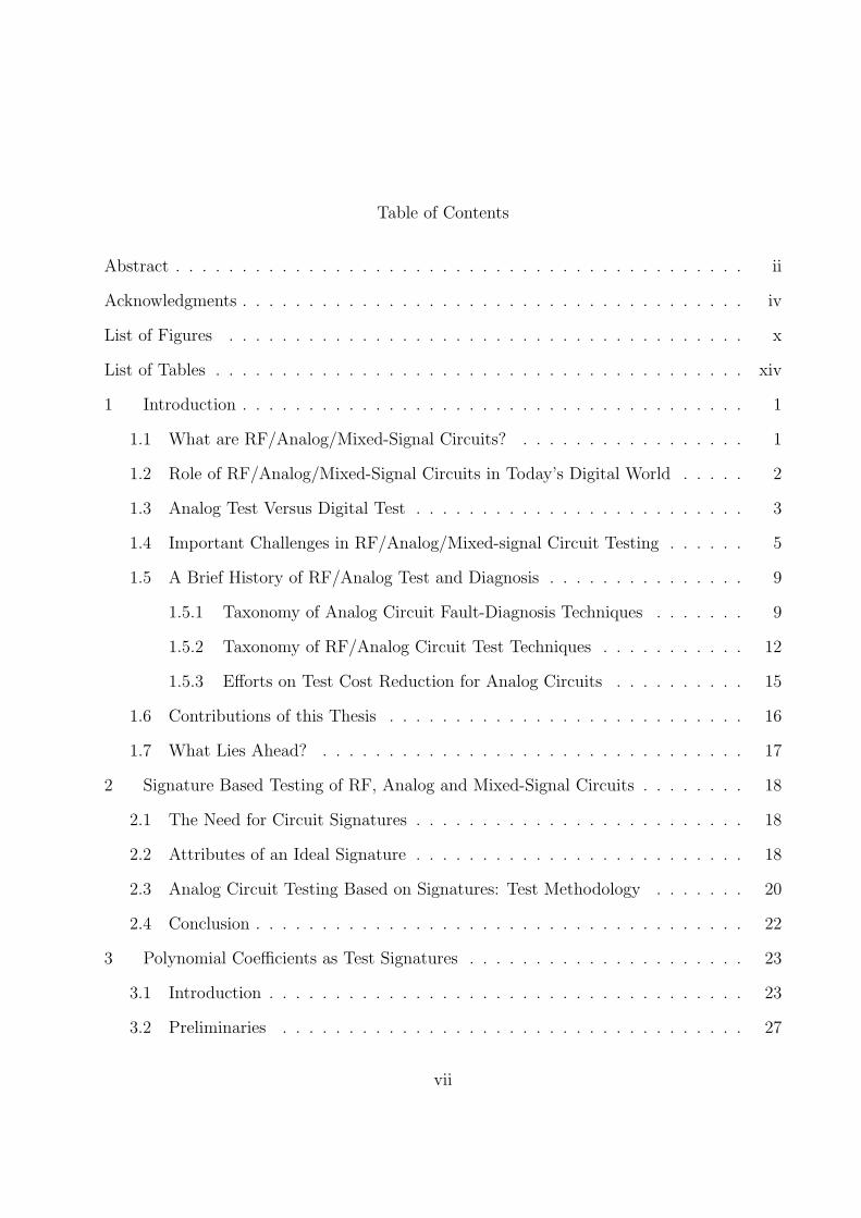
Table of Contents
Abstract . . . . . . . . . . . . . . . . . . . . . . . . . . . . . . . . . . . . . . . . . . . ii
Acknowledgments . . . . . . . . . . . . . . . . . . . . . . . . . . . . . . . . . . . . . . iv
List of Figures . . . . . . . . . . . . . . . . . . . . . . . . . . . . . . . . . . . . . . . x
List of Tables . . . . . . . . . . . . . . . . . . . . . . . . . . . . . . . . . . . . . . . . xiv
1 Introduction . . . . . . . . . . . . . . . . . . . . . . . . . . . . . . . . . . . . . . 1
1.1 What are RF/Analog/Mixed-Signal Circuits? . . . . . . . . . . . . . . . . . 1
1.2 Role of RF/Analog/Mixed-Signal Circuits in Today’s Digital World . . . . . 2
1.3 Analog Test Versus Digital Test . . . . . . . . . . . . . . . . . . . . . . . . . 3
1.4 Important Challenges in RF/Analog/Mixed-signal Circuit Testing . . . . . . 5
1.5 A Brief History of RF/Analog Test and Diagnosis . . . . . . . . . . . . . . . 9
1.5.1 Taxonomy of Analog Circuit Fault-Diagnosis Techniques . . . . . . . 9
1.5.2 Taxonomy of RF/Analog Circuit Test Techniques . . . . . . . . . . . 12
1.5.3 Efforts on Test Cost Reduction for Analog Circuits . . . . . . . . . . 15
1.6 Contributions of this Thesis . . . . . . . . . . . . . . . . . . . . . . . . . . . 16
1.7 What Lies Ahead? . . . . . . . . . . . . . . . . . . . . . . . . . . . . . . . . 17
2 Signature Based Testing of RF, Analog and Mixed-Signal Circuits . . . . . . . . 18
2.1 The Need for Circuit Signatures . . . . . . . . . . . . . . . . . . . . . . . . . 18
2.2 Attributes of an Ideal Signature . . . . . . . . . . . . . . . . . . . . . . . . . 18
2.3 Analog Circuit Testing Based on Signatures: Test Methodology . . . . . . . 20
2.4 Conclusion . . . . . . . . . . . . . . . . . . . . . . . . . . . . . . . . . . . . . 22
3 Polynomial Coefficients as Test Signatures . . . . . . . . . . . . . . . . . . . . . 23
3.1 Introduction . . . . . . . . . . . . . . . . . . . . . . . . . . . . . . . . . . . . 23
3.2 Preliminaries . . . . . . . . . . . . . . . . . . . . . . . . . . . . . . . . . . . 27
vii

3.2.1 Analysis of Polynomial Coefficients . . . . . . . . . . . . . . . . . . . 27
3.2.2 Definitions . . . . . . . . . . . . . . . . . . . . . . . . . . . . . . . . . 29
3.3 Problem Description and Sketch of Solution . . . . . . . . . . . . . . . . . . 29
3.4 Generalization . . . . . . . . . . . . . . . . . . . . . . . . . . . . . . . . . . . 32
3.5 Experimental Results . . . . . . . . . . . . . . . . . . . . . . . . . . . . . . . 33
3.6 Fault Diagnosis . . . . . . . . . . . . . . . . . . . . . . . . . . . . . . . . . . 42
3.6.1 Computation of Sensitivities . . . . . . . . . . . . . . . . . . . . . . . 43
3.6.2 Diagnosing Parametric Faults . . . . . . . . . . . . . . . . . . . . . . 43
3.6.3 Deducing Faults . . . . . . . . . . . . . . . . . . . . . . . . . . . . . . 44
3.7 Conclusion . . . . . . . . . . . . . . . . . . . . . . . . . . . . . . . . . . . . . 44
4 V-Transform Coefficients as Test Signatures . . . . . . . . . . . . . . . . . . . . 48
4.1 Introduction . . . . . . . . . . . . . . . . . . . . . . . . . . . . . . . . . . . . 48
4.2 Background . . . . . . . . . . . . . . . . . . . . . . . . . . . . . . . . . . . . 51
4.3 The V-Transform . . . . . . . . . . . . . . . . . . . . . . . . . . . . . . . . . 53
4.4 A Problem and an Approach . . . . . . . . . . . . . . . . . . . . . . . . . . . 53
4.5 Generalization . . . . . . . . . . . . . . . . . . . . . . . . . . . . . . . . . . . 56
4.6 Fault Diagnosis . . . . . . . . . . . . . . . . . . . . . . . . . . . . . . . . . . 58
4.7 Simulation Results . . . . . . . . . . . . . . . . . . . . . . . . . . . . . . . . 59
4.8 Experimental Verification . . . . . . . . . . . . . . . . . . . . . . . . . . . . 62
4.8.1 Test Setup . . . . . . . . . . . . . . . . . . . . . . . . . . . . . . . . . 63
4.8.2 Measured Results . . . . . . . . . . . . . . . . . . . . . . . . . . . . . 64
4.9 Sumamrizing V-Transform . . . . . . . . . . . . . . . . . . . . . . . . . . . . 66
5 Probability Moments as Test Signatures . . . . . . . . . . . . . . . . . . . . . . 67
5.1 Introduction . . . . . . . . . . . . . . . . . . . . . . . . . . . . . . . . . . . . 67
5.2 Background . . . . . . . . . . . . . . . . . . . . . . . . . . . . . . . . . . . . 69
5.2.1 Moment Generating Functions . . . . . . . . . . . . . . . . . . . . . . 69
5.2.2 Random Variable Transformation . . . . . . . . . . . . . . . . . . . . 70
viii
5.2.3 Minimum Size Detectable Fault . . . . . . . . . . . . . . . . . . . . . 72
5.3 Problem and Approach . . . . . . . . . . . . . . . . . . . . . . . . . . . . . . 72
5.4 Generalization . . . . . . . . . . . . . . . . . . . . . . . . . . . . . . . . . . . 75
5.5 Fault Detection in Elliptic Filter . . . . . . . . . . . . . . . . . . . . . . . . . 76
5.6 Fault Diagnosis . . . . . . . . . . . . . . . . . . . . . . . . . . . . . . . . . . 78
5.7 Fault Diagnosis in Low Noise Amplifier . . . . . . . . . . . . . . . . . . . . . 80
5.8 Conclusion . . . . . . . . . . . . . . . . . . . . . . . . . . . . . . . . . . . . . 81
6 Bounds on Fault Coverage and Defect Level in Signature Based Testing . . . . . 85
6.1 Introduction . . . . . . . . . . . . . . . . . . . . . . . . . . . . . . . . . . . . 85
6.2 Problem Formulation . . . . . . . . . . . . . . . . . . . . . . . . . . . . . . . 87
6.3 Our Approach . . . . . . . . . . . . . . . . . . . . . . . . . . . . . . . . . . . 89
6.3.1 Bounding Defect level . . . . . . . . . . . . . . . . . . . . . . . . . . 89
6.3.2 Bounding Fault Coverage . . . . . . . . . . . . . . . . . . . . . . . . 92
6.4 Simulation and Computation . . . . . . . . . . . . . . . . . . . . . . . . . . . 94
6.5 Simulation Versus Optimization: A Trade-off . . . . . . . . . . . . . . . . . . 97
6.6 Conclusion . . . . . . . . . . . . . . . . . . . . . . . . . . . . . . . . . . . . . 99
7 Conclusion . . . . . . . . . . . . . . . . . . . . . . . . . . . . . . . . . . . . . . . 101
7.1 Thoughts on Future Work . . . . . . . . . . . . . . . . . . . . . . . . . . . . 101
7.1.1 Adaptive Test With Signatures . . . . . . . . . . . . . . . . . . . . . 102
7.1.2 Preliminary Experiments . . . . . . . . . . . . . . . . . . . . . . . . . 102
7.1.3 Estimating Defect Level in Analog and Radio-Frequency Circuit Testing104
Bibliography . . . . . . . . . . . . . . . . . . . . . . . . . . . . . . . . . . . . . . . . 106
A Some Theorems on Nonlinear Systems . . . . . . . . . . . . . . . . . . . . . . . 116
B Output Variance of RC Filter . . . . . . . . . . . . . . . . . . . . . . . . . . . . 119
ix

List of Figures
1.1 Distribution of input/output functions of different types of circuits. . . . . . . . 2
1.2 Hypothetical picture illustrating different blocks that make use of analog/RF
modules in a typical RF-SoC (for mobile devices). . . . . . . . . . . . . . . . . . 3
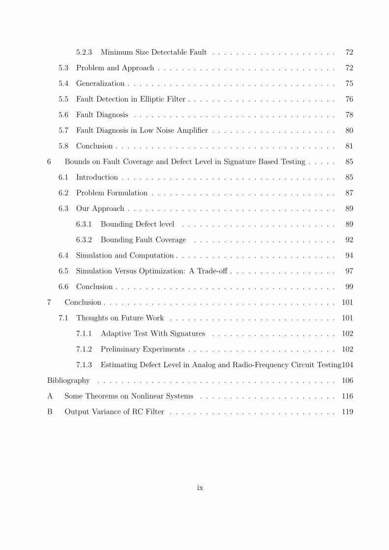
1.3 Mixed-signal System-on-Chip (SoC) showing size of analog block as a fraction of
total die area. Analog interface contributes to about 30% of the total die area.
Chip micrograph courtesy of Neolinear [107]. . . . . . . . . . . . . . . . . . . . . 5
1.4 Mixed-signal System-on-Chip (SoC) showing size of analog block as a fraction of
total die area. Analog interface contributes to about 12% of the total die area.
Chip micrograph courtesy of Frank Op’t Eynde, Alcatel [107]. . . . . . . . . . . 6
1.5 Manufacturing cost per transistor on a die has steadily decreased, while test cost
per transistor has remained almost constant [1, 2]. Around 2014, it is expected
that testing a transistor will cost more than manufacturing one. Also of note is
that the analog/mixed-signal test cost per transistor is almost 10 times that of
the digital test cost per transistor. . . . . . . . . . . . . . . . . . . . . . . . . . 7
1.6 A possible classification of analog circuit fault-diagnosis techniques [17]. . . . . . 10
1.7 A possible classification of analog circuit test techniques. . . . . . . . . . . . . . 12
1.8 Specification testing of analog/mixed-signal circuits in a production test setting. 13
x

2.1 Scatter plot of measurements showing the signature on the X-axis and the circuit
specification on the Y-axis. An ideal signature will have all points lined up along
a straight line such that there is perfect correlation between the signature and
the specification. . . . . . . . . . . . . . . . . . . . . . . . . . . . . . . . . . . . 19
3.1 A second order low pass filter. . . . . . . . . . . . . . . . . . . . . . . . . . . . . 24
3.2 Cascade amplifier . . . . . . . . . . . . . . . . . . . . . . . . . . . . . . . . . . . 25
3.3 Flow chart showing fault simulation process and bounding of coefficients. . . . . 34
3.4 Flow chart outlining test procedure for CUT. . . . . . . . . . . . . . . . . . . . 35
3.5 Elliptic filter. . . . . . . . . . . . . . . . . . . . . . . . . . . . . . . . . . . . . . 36
3.6 DC response of elliptic filter with curve fitting polynomial. . . . . . . . . . . . . 37
3.7 Curve-fit polynomial with coefficients at frequency = 100Hz. . . . . . . . . . . . 37
3.8 Curve-fitting polynomial with coefficients at frequency = 900Hz. . . . . . . . . . 38
3.9 Curve-fitting polynomial with coefficients at frequency = 1000Hz. . . . . . . . . 38
3.10 Curve-fitting polynomial with coefficients at frequency = 1100Hz. . . . . . . . . 39
3.11 Mapping showing one possible relation between various parameters and coefficients. 39
3.12 Low noise amplifier (LNA) schematic. . . . . . . . . . . . . . . . . . . . . . . . 40
3.13 I/O response of LNA at four frequencies. . . . . . . . . . . . . . . . . . . . . . . 41
3.14 Comparison of I/O plots of LNA at 3 different values of load resistance RL =
95kΩ, 100kΩ (nominal), and 105kΩ. . . . . . . . . . . . . . . . . . . . . . . . . 41
4.1 Cascade amplifier. . . . . . . . . . . . . . . . . . . . . . . . . . . . . . . . . . . 54
xi

4.2 Fault simulation process and bounding of coefficients (Flowchart I), and complete
test procedure (Flowchart II). . . . . . . . . . . . . . . . . . . . . . . . . . . . . 57
4.3 Probability distribution of polynomial coefficient C under a parametric fault (bro-
ken line) as opposed to that with only process variation (solid line). . . . . . . . 59
4.4 Elliptic filter. . . . . . . . . . . . . . . . . . . . . . . . . . . . . . . . . . . . . . 60
4.5 DC response of elliptic filter with curve fitting polynomial and V-transform plot. 61
4.6 Test setup with elliptic filter built on the prototyping board, which is in turn
mounted on the NI ELVISII+ bench-top module. Voltage and frequency control
of the applied signal is handled through the PC which is connected through USB
port to the bench-top module. Output from the circuit is sampled and transferred
through the same USB connection to the PC (where it can be post-processed).
Also, circuit output can be displayed on the PC using a virtual oscilloscope utility
available in the ELVIS software (see Figure 4.7). . . . . . . . . . . . . . . . . . . 63
4.7 Input/output, to/from the elliptic filter displayed on the PC based virtual oscil-
loscope at a frequency f = 100Hz. . . . . . . . . . . . . . . . . . . . . . . . . . 64
5.1 Moments of different orders as functions of input noise power (standard deviation
of input RV) with (in red/dashed) and without (in blue/solid) RV transformation
for first order RC filter. See Figure 5.2. . . . . . . . . . . . . . . . . . . . . . . . 71
5.2 First-order RC filter. . . . . . . . . . . . . . . . . . . . . . . . . . . . . . . . . . 72
5.3 A cascade amplifier. . . . . . . . . . . . . . . . . . . . . . . . . . . . . . . . . . 73
5.4 Block diagram of a system with CUT using white noise excitation. . . . . . . . 76
5.5 Fault simulation process and bounding of moments (Flowchart I), and the com-
plete test procedure (Flowchart II). . . . . . . . . . . . . . . . . . . . . . . . . . 77
xii

5.6 Elliptic filter. . . . . . . . . . . . . . . . . . . . . . . . . . . . . . . . . . . . . . 78
5.7 Fault simulation (Flowchart I) and Fault diagnosis (Flowchart II) procedures
summarized. . . . . . . . . . . . . . . . . . . . . . . . . . . . . . . . . . . . . . 79
5.8 Schematic of low noise amplifier. . . . . . . . . . . . . . . . . . . . . . . . . . . 82
6.1 Hypercube around coefficient Ck and associated regions. . . . . . . . . . . . . . 88
6.2 Defect level (DL) as a function of number of components (N). . . . . . . . . . . 95
6.3 Defect level (DL) plotted against ratio of coefficient of uncertainty to tolerance
of components ( ϵσ). . . . . . . . . . . . . . . . . . . . . . . . . . . . . . . . . . . 96
6.4 RC ladder filter network of n stages. . . . . . . . . . . . . . . . . . . . . . . . . 97
6.5 Comparison of defect level bounds with simulated value ( ϵσ= 0.1) for RC ladder
filter network. . . . . . . . . . . . . . . . . . . . . . . . . . . . . . . . . . . . . . 98
6.6 CPU time (in seconds) to compute NMSDF by simulation versus coefficient of
uncertainty, ϵ. . . . . . . . . . . . . . . . . . . . . . . . . . . . . . . . . . . . . . 100
7.1 Block diagram of the adaptive test system based on circuit signatures. . . . . . 103
7.2 Scatter plot of tested devices showing defect level and yield loss for the open loop
signature test, where the input stimulus is not tuned adaptively. . . . . . . . . . 104
7.3 Scatter plot of tested devices showing defect level and yield loss for the closed
loop signature test, where the input stimulus is tuned adaptively. . . . . . . . . 105
A.1 A possible system model for a non-linear circuit. . . . . . . . . . . . . . . . . . 117
A.2 Non-linear, non-monotonic function decomposed into piecewise monotonic func-
tions. . . . . . . . . . . . . . . . . . . . . . . . . . . . . . . . . . . . . . . . . . 118
B.1 First order RC low-pass filter. . . . . . . . . . . . . . . . . . . . . . . . . . . . . 119
xiii

List of Tables
3.1 MSDF for cascade amplifier of Figure 3.2 with α = 0.05. . . . . . . . . . . . . . 32
3.2 LNA specification. . . . . . . . . . . . . . . . . . . . . . . . . . . . . . . . . . . 40
3.3 Parameter combinations leading to maximum values of coefficients with α = 0.05for the LNA. . . . . . . . . . . . . . . . . . . . . . . . . . . . . . . . . . . . . . 42
3.4 Parameter combinations leading to Min values of coefficients with α = 0.05 forthe LNA. . . . . . . . . . . . . . . . . . . . . . . . . . . . . . . . . . . . . . . . 43
3.5 Parameter combinations leading to Max and Min Values of coefficients with α =0.05 at 1000Hz for the elliptic filter. . . . . . . . . . . . . . . . . . . . . . . . . . 45
3.6 Results of some injected faults at different frequencies for the elliptic filter. . . . 46
3.7 Parametric fault fiagnosis with confidence levels of ≈ 98.9% for the elliptic filter. 47
3.8 Results of test and diagnosis of some injected faults for LNA. . . . . . . . . . . 47
4.1 MSDF for cascade amplifier of Figure 4.1 with α = 0.05. . . . . . . . . . . . . . 56
4.2 Parameter combinations leading to maximum values of V-transform coefficientswith α = 0.05 for the elliptic filter. . . . . . . . . . . . . . . . . . . . . . . . . . 60
4.3 Parameter combinations leading to minimum values of V-transform coefficientswith α = 0.05 for the elliptic filter. . . . . . . . . . . . . . . . . . . . . . . . . . 61
4.4 Results for some injected faults in the elliptic filter. . . . . . . . . . . . . . . . . 62
4.5 Parametric fault diagnosis with confidence levels of ≈ 88% for the elliptic filter. 62
4.6 Measured results for some injected faults in elliptic filter. . . . . . . . . . . . . . 65
5.1 MSDF for cascade amplifier of Figure 5.3 with µ0 = 0.05. . . . . . . . . . . . . . 75
5.2 Parameter combinations leading to maximum values of moments with devicetolerance γ = 0.05 in elliptic filter. . . . . . . . . . . . . . . . . . . . . . . . . . 80
xiv

5.3 Parameter combinations leading to minimum values of moments with device tol-erance γ = 0.05 in elliptic filter. . . . . . . . . . . . . . . . . . . . . . . . . . . . 83
5.4 Fault detection of some injected faults in elliptic filter. . . . . . . . . . . . . . . 83
5.5 Fault dictionary for catastrophic faults in low noise amplifier. . . . . . . . . . . 84
6.1 Defect level and fault coverage of benchmark circuits obtained from computationand simulation. For brevity in the table, T: Transistor, O: Opamp, R: Resistor,C: Capacitor, N : Total number of components. . . . . . . . . . . . . . . . . . . 98
7.1 Comparison of defect level, yield loss, and test time for actual specification test,signature test in open loop, and signature test in closed loop. . . . . . . . . . . 103
xv
Chapter 1
Introduction
1.1 What are RF/Analog/Mixed-Signal Circuits?
“RF/Analog/Mixed-signal” is a label associated with circuits that have a portion of
their operating input, or output, or both input and output, consisting of continuous-time,
continuous-amplitude signals, as opposed to digital circuits that have both their operating
input and output consisting of discrete-time, quantized-amplitude (Boolean) signals.
RF circuits can be broadly classified as circuits that process signals in the high-frequency
(ranging from a low of 20 kHz all the way up to 60 GHz or higher) domain. Examples include
low noise amplifier (LNA), mixer, filter, and voltage controlled oscillator among others.
Analog circuits are a bigger class of circuits, in that, they encompass all continuous-
time, continuous-amplitude signal processing circuits. As such RF circuits can be thought of
as a subset of analog circuits operating in the high-frequency range [103]. Examples include
dc power supply circuits such as regulators, op-amps, and signals conditioning circuits.
Mixed-signal circuits are those that function as a bridge between the digital and the
analog worlds, in that one of their operating input (output) is continuous-time, continuous-
amplitude (known as analog) signal, while the output (input) is discrete-time, discrete-
amplitude (known as digital) signal. Examples include analog-to-digital converters (in-
put = analog, output = digital), and digital-to-analog converters (input = digital, out-
put = analog). Digital circuits have both their inputs and outputs in the discrete-time
discrete-amplitude domain. Figure 1.1 illustrates the input/output domain distribution of
RF/analog/mixed-signal and digital circuits with example circuits for each type.
1

Figure 1.1: Distribution of input/output functions of different types of circuits.
1.2 Role of RF/Analog/Mixed-Signal Circuits in Today’s Digital World
The nature of information produced in the world around us is analog, that is, the
myriad information sources–such as sensors, be it video, audio, heat, light, or radio frequency
(RF)–generate signals in a continuous-amplitude, continuous-time fashion. On the other
hand, today’s computing is leveraging the digital microprocessor revolution where most
computation happens digitally in a large monolithic piece of silicon. Consequently, any
processing of these signals calls for a bridge between the analog and digital worlds. Analog-
to-digital converter (fittingly named) is a typical circuit that functions as a bridge. There
are many other analog circuits needed before the signal becomes bridgeable like signal-
conditioning circuits that make use of amplifiers, filters and so on.
Similarly, the radio waves transmitted in free air by today’s ubiquitous cell-phones are
relayed by virtue of those waves being high-frequency analog signals [74]. At the trans-
mitting as well as the receiving end of such a wireless communication system, processing
2

Figure 1.2: Hypothetical picture illustrating different blocks that make use of analog/RFmodules in a typical RF-SoC (for mobile devices).
(coding/decoding) of radio signals is accomplished by several RF or analog circuit blocks
such as low noise amplifiers, phase-locked loops, mixers, and filters [104].
Analog amplifiers are also used at the digital chip boundaries acting as buffers to drive
the pins with adequate amounts of current [50]. Direct-current (dc) power-supply required
to power digital or analog circuits are composed of analog circuitry. Virtually any system-
on-chip (SoC) or custom integrated circuit conceivable ends up having a portion of analog
circuitry for accomplishing one or more of the tasks noted above. In other words, analog is
everywhere in todays digital world. Figure 1.2 shows the RF/analog circuit portions in a
typical RF-SoC of today. Notice that RF/analog circuits contribute to roles from powering
up the chip to enabling communication with the external world.
1.3 Analog Test Versus Digital Test
Digital circuits have succinct fault models (like the stuck-at fault) allowing the use of
“structural” tests that target specific faults instead of testing for the entire functionality
of the circuit. They serve as effective replacements of functional tests, thereby obviating
long test times that would have otherwise been necessary for running functional tests even
on a moderately-sized digital circuit. Consider for example an n-input, m-output, g-gate
3

digital circuit (without memory elements like flip-flops); testing such a circuit exhaustively
for functionality can take 2n vectors in the worst-case [33]. Clearly the number of vectors
needed to test the circuit is exponential in the number of inputs in the circuit. On the other
hand by targeting faults individually (based on a fault model), the number of test vectors
needed to test the complete circuit is bounded by the number of faults to be targeted.
For this example, it is of the order of m + n + g. Consequently, fault model based tests
considerably reduce the number of test vectors needed when compared to functional tests
for large digital circuits. Common structural defects (e.g., signal line short to power and/or
ground rails or other signal lines) in integrated circuits are easier to model as faults in digital
circuits due to the fact that the deviant behavior in the presence of a fault can be defined
concisely (for example, as an incorrect logic value, of which there are only two possibilities–1
or 0) at any node in the digital circuit. This simplicity in fault-modeling is an important
factor contributing to the prevalence of structural testing in digital circuits.
In contrast, analog circuits propagate signals through them in a continuum of signal
values, requiring a large number of test signals to test the circuit. The deviant behavior in
a faulty analog circuit can take a whole spectrum of incorrect values. For example, if the
acceptable range of voltage at some node in an analog circuit is [Vnom − Vtol, Vnom + Vtol],
then the faulty behavior can take a whole spectrum of values outside this nominal range.
One possible fault model for this situation could be to have a resistor tied to the supply rail
and changing the value of that resistor to emulate the incorrect spectrum of voltage values.
Unfortunately, there is no one resistance value (or fault-size) that can change the voltage at
the node to all incorrect values in the spectrum.
A number of resistor values have to be used to sample the faulty voltage spectra suf-
ficiently. So a large number of fault-injections may be necessary to model a fault even at
a single node of an analog circuit. This complexity of fault models makes the model-based
testing of analog circuits an unsuitable proposition. The prevalent practice in the industry
is to use a large set of signals to functionally qualify or test the circuit. Applying these test
4
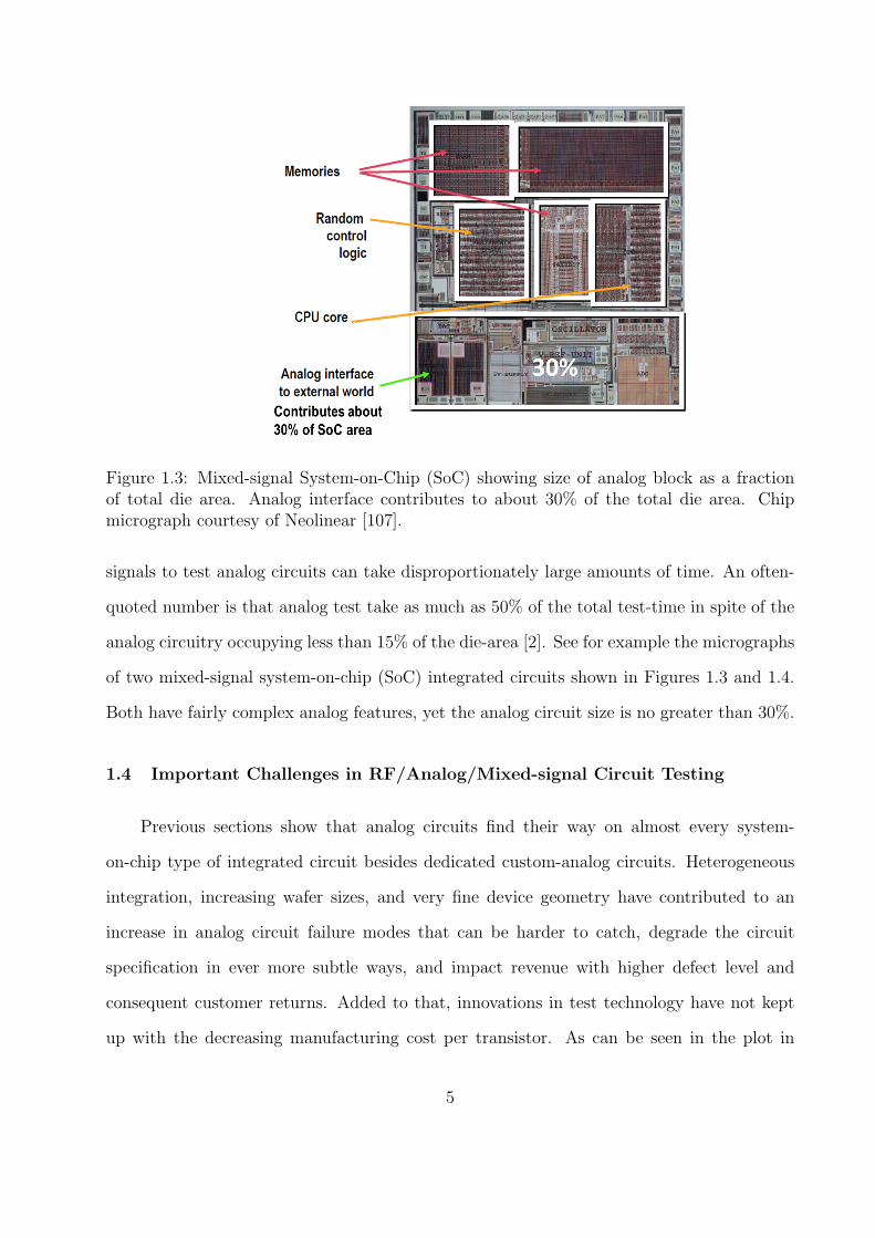
Figure 1.3: Mixed-signal System-on-Chip (SoC) showing size of analog block as a fractionof total die area. Analog interface contributes to about 30% of the total die area. Chipmicrograph courtesy of Neolinear [107].
signals to test analog circuits can take disproportionately large amounts of time. An often-
quoted number is that analog test take as much as 50% of the total test-time in spite of the
analog circuitry occupying less than 15% of the die-area [2]. See for example the micrographs
of two mixed-signal system-on-chip (SoC) integrated circuits shown in Figures 1.3 and 1.4.
Both have fairly complex analog features, yet the analog circuit size is no greater than 30%.
1.4 Important Challenges in RF/Analog/Mixed-signal Circuit Testing
Previous sections show that analog circuits find their way on almost every system-
on-chip type of integrated circuit besides dedicated custom-analog circuits. Heterogeneous
integration, increasing wafer sizes, and very fine device geometry have contributed to an
increase in analog circuit failure modes that can be harder to catch, degrade the circuit
specification in ever more subtle ways, and impact revenue with higher defect level and
consequent customer returns. Added to that, innovations in test technology have not kept
up with the decreasing manufacturing cost per transistor. As can be seen in the plot in
5

Figure 1.4: Mixed-signal System-on-Chip (SoC) showing size of analog block as a fractionof total die area. Analog interface contributes to about 12% of the total die area. Chipmicrograph courtesy of Frank Op’t Eynde, Alcatel [107].
Figure 1.5, test cost has remained fairly constant with the passing of years, while the cost
of manufacturing a transistor has dropped steadily [1]. Furthermore, though analog circuits
contribute less than 10-20% of the chip area, they account for over 50% of the test cost [2].
This can also be noticed in from the plot in Figure 1.5 where the analog test cost per
transistor is almost an order of magnitude higher than digital test cost per transistor.
Test cost stemming from long test-times on expensive ATE is the underlying theme of
important test problems in analog/mixed signal circuits.
1. Non-linear, continuous-time, continuous-amplitude nature of analog circuits:
Most analog circuits are non-linear, continuous-time, and continuous amplitude in
nature and that makes it a computational challenge to both implement automatic test
generation algorithms, and store the large amounts of waveform data that is to be
applied to the circuit-under-test in a production test environment.
6

1980 1985 1990 1995 2000 2005 2010 201510
−2
10−1
100
101
102
103
104
Cos
t: C
ents
/10,
000
tran
sist
ors
Manufacturing costAnalog/Mixed−signal test costDigital test cost
Figure 1.5: Manufacturing cost per transistor on a die has steadily decreased, while test costper transistor has remained almost constant [1, 2]. Around 2014, it is expected that testinga transistor will cost more than manufacturing one. Also of note is that the analog/mixed-signal test cost per transistor is almost 10 times that of the digital test cost per transistor.
2. “Functionally-good-enough” testing does not cut the deal:
Testing if a circuit is good-enough (or functional) for some specifications can be rel-
atively easy, but extracting the absolute value of that specification can involve sig-
nificantly higher effort. For example, in specification testing an RF transceiver, the
circuit can be qualified as good if it passes a simple loop-back test. In a loop-back test,
the transmitter is tied back to the receiver and the transceiver is considered “pass,”
if it meets all the receiver specifications, but to make sure that its specifications meet
all the regulatory compliance requirements and binning it within a performance bin
can be more difficult. Further not all wireless standards permit concurrent operation
of transmit and receive modes in a transceiver (which is a prerequisite for loop-back
test), and designing the circuit enable this capability can involve major design effort
and consequent cost.
7

3. Inadequate signal visibility at the circuit output:
Analog circuits for specific functions can be small and deeply embedded within a larger
circuit. Bringing out these signals to the pads without degrading the signal quality can
be a challenge. Further the measurement inaccuracies due to noise (and consequent
lack of repeatability) may call for longer measurement times to average out any noise
induced errors. Such measurement errors due to noise is uncommon in digital circuits
due to the inherent noise margins.
4. Process variation has made life difficult not only for designers, but also for test engi-
neers:
Random manufacturing process variation can have significant impact on analog perfor-
mance parameters. This is because analog circuits are designed with stringent match-
ing requirements (for example, transistors in both the legs of a current-mirror cir-
cuit [50, 51] should be a replica of each other lest we risk a high offset current in one
branch and the resulting non-linearity if the circuit were to be used in an amplifier).
Traditionally testing for sizable manufacturing defects has been the primary concern
during test. With process variation induced local variation of circuit parameters, distin-
guishing between random process variations and recurring small manufacturing defects
can be difficult if the deviation in nominal functional performance and defective cir-
cuits is small. This is an important concern in analog circuits much like the problem
encountered in distinguishing small-delay faults from process variation induced delay
faults in digital circuits.
In the next section, we review the efforts spent on RF/Analog circuit testing and diag-
nosis since the early second-half of the twentieth century.
8
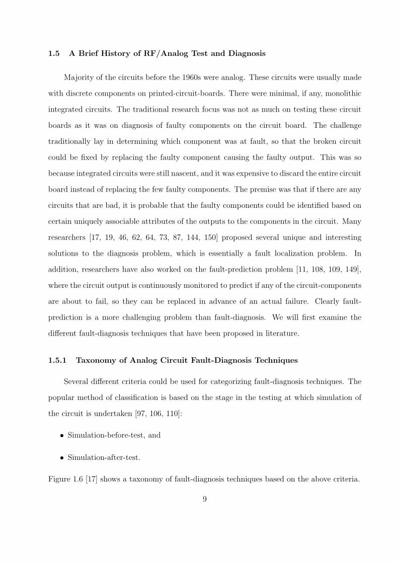
1.5 A Brief History of RF/Analog Test and Diagnosis
Majority of the circuits before the 1960s were analog. These circuits were usually made
with discrete components on printed-circuit-boards. There were minimal, if any, monolithic
integrated circuits. The traditional research focus was not as much on testing these circuit
boards as it was on diagnosis of faulty components on the circuit board. The challenge
traditionally lay in determining which component was at fault, so that the broken circuit
could be fixed by replacing the faulty component causing the faulty output. This was so
because integrated circuits were still nascent, and it was expensive to discard the entire circuit
board instead of replacing the few faulty components. The premise was that if there are any
circuits that are bad, it is probable that the faulty components could be identified based on
certain uniquely associable attributes of the outputs to the components in the circuit. Many
researchers [17, 19, 46, 62, 64, 73, 87, 144, 150] proposed several unique and interesting
solutions to the diagnosis problem, which is essentially a fault localization problem. In
addition, researchers have also worked on the fault-prediction problem [11, 108, 109, 149],
where the circuit output is continuously monitored to predict if any of the circuit-components
are about to fail, so they can be replaced in advance of an actual failure. Clearly fault-
prediction is a more challenging problem than fault-diagnosis. We will first examine the
different fault-diagnosis techniques that have been proposed in literature.
1.5.1 Taxonomy of Analog Circuit Fault-Diagnosis Techniques
Several different criteria could be used for categorizing fault-diagnosis techniques. The
popular method of classification is based on the stage in the testing at which simulation of
the circuit is undertaken [97, 106, 110]:
• Simulation-before-test, and
• Simulation-after-test.
Figure 1.6 [17] shows a taxonomy of fault-diagnosis techniques based on the above criteria.
9

Figure 1.6: A possible classification of analog circuit fault-diagnosis techniques [17].
Fault Dictionary Based Diagnosis
Fault-dictionary techniques classified under simulation-before-test techniques in Fig-
ure 1.6 are similar to the widely used fault-dictionary based diagnosis approaches for digital
circuits [7, 33]. The first step is to define the most likely faults that can be expected in
a given circuit. Defining faults is an important step as the dictionary-size is limited by
number of faults defined. An appropriate number of test responses are then captured by
simulating the circuit-under-test (CUT) by injecting the defined faults one-by-one, such
that unique identification of each fault can be possible by deductive reasoning based on the
captured responses for all the applied tests before actually subjecting the circuit in question
to test. At the time of test, the captured responses are used to identify the fault or local-
ize it to a small ‘ambiguity-set’ of faults. The test responses can be captured in frequency
domain [31, 88, 89, 133, 148] or in the time domain [113, 132, 147], or as a combination of
both [78, 114].
10

Diagnosis Based on Parameter Identification Techniques
Parameter identification techniques, grouped under simulation-after-test approach in
Figure 1.6 involves estimating the deviation in nominal values of circuit components based
on voltage/current measurements made at specific nodes in the circuit-under-test for a known
input response. The nominal component values and topology of circuit-under-test is known
a priori. The deviations in the component values from their nominal values is uniquely
determined by solving the set of linear or non-linear equations of the circuit (as determined
by the circuit topology). Such circuits for which component values are uniquely determinable
based on a few measurements are said to be element-value-solvable [20, 21, 22] circuits and
are amenable to parameter identification techniques.
Diagnosis Based on Fault Verification Techniques
Fault verification techniques are based on the premise that for a circuit of nc components,
with nm measurements taken at test, all the faulty elements (nf in number) can be uniquely
identifiable if nf is very small, such that the inequality nf << nm < nc is satisfied. The
faulty elements are identified by checking the consistency of certain equations which are
invariant on the changes in the faulty component values [49, 69, 105, 146].
Approximation Techniques for Diagnosis
Approximation techniques are able to localize faults with limited number of measure-
ments. Two prominent types of approximation techniques are probabilistic [30, 71] and
optimization-based [60, 81, 102]. In probabilistic diagnosis techniques all the circuit fault-
simulation is done before test and can be classified under simulation-before-test. Their work-
ing principles are very similar to the dictionary based approach. Optimization techniques,
on the other hand, optimize some pre-determined criterion to find the most likely faulty
element. For example, the L2 approximation technique [81, 102] uses weighted least squares
11

Figure 1.7: A possible classification of analog circuit test techniques.
criterion in identifying the–most-likely faulty element–the element that has undergone the
largest deviation from its nominal value.
However, with the advent of integrated circuits, things began to change. Cost of man-
ufacturing even complex circuits, with fairly large component counts, was cheaper than
building the bulky boards. The focus slowly shifted from finding the faulty component, or
diagnosis, to finding out if the overall circuit behaved as it was designed to behave. We will
now examine taxonomy of efforts in analog circuit testing that are geared towards different
aspects of the test problem, all of which can be either categorized as aiming to reduce the
analog test cost, or increase the testability of the circuit and test-quality.
1.5.2 Taxonomy of RF/Analog Circuit Test Techniques
Figure 1.7 shows the taxonomy of test techniques for analog/RF circuits. The different
analog test techniques that are proposed in literature can be classified under three broad
categories: functional, structural, and alternate (combination of functional and structural)
testing. We shall now review each of the categories and sampling of different test techniques
that have been proposed under each of those categories.
12
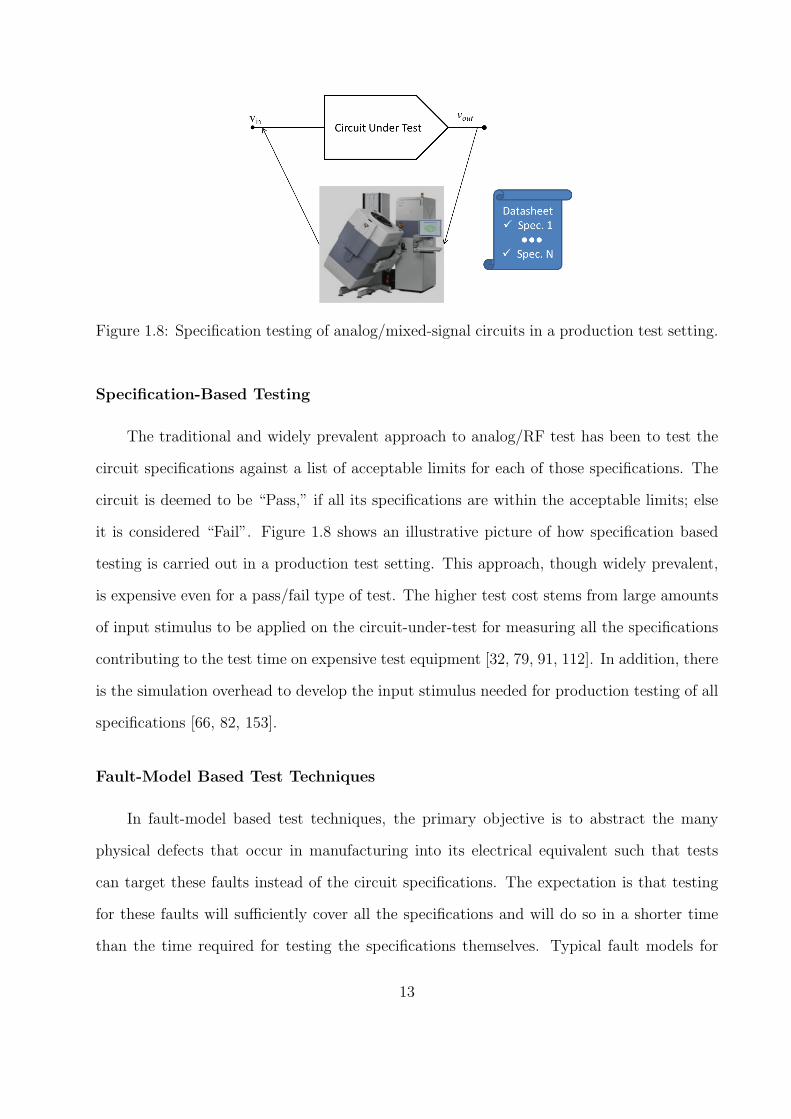
Figure 1.8: Specification testing of analog/mixed-signal circuits in a production test setting.
Specification-Based Testing
The traditional and widely prevalent approach to analog/RF test has been to test the
circuit specifications against a list of acceptable limits for each of those specifications. The
circuit is deemed to be “Pass,” if all its specifications are within the acceptable limits; else
it is considered “Fail”. Figure 1.8 shows an illustrative picture of how specification based
testing is carried out in a production test setting. This approach, though widely prevalent,
is expensive even for a pass/fail type of test. The higher test cost stems from large amounts
of input stimulus to be applied on the circuit-under-test for measuring all the specifications
contributing to the test time on expensive test equipment [32, 79, 91, 112]. In addition, there
is the simulation overhead to develop the input stimulus needed for production testing of all
specifications [66, 82, 153].
Fault-Model Based Test Techniques
In fault-model based test techniques, the primary objective is to abstract the many
physical defects that occur in manufacturing into its electrical equivalent such that tests
can target these faults instead of the circuit specifications. The expectation is that testing
for these faults will sufficiently cover all the specifications and will do so in a shorter time
than the time required for testing the specifications themselves. Typical fault models for
13

analog circuits are component opens and shorts that mimic large defects that can signifi-
cantly deviate the behavior of the component. Such faults are known as catastrophic faults.
Examples of catastrophic faults can be resistor open or short. Defects that lead to small
deviations in functionality of the circuit components are modeled as fractional drifts from
the nominal values of the circuit element (usually beyond the component tolerance limit),
and are called parametric faults or soft faults. Examples of parametric faults can be ±10%
deviation in the nominal value of the resistor. Number of such fault models have been de-
veloped for different components in analog circuits [141]. Different fault-model based test
schemes [29, 36, 53, 55, 57, 58, 80, 90, 100, 101, 130, 131] have been proposed in literature.
We briefly discuss a representative set of these techniques.
Sensitivity based test and diagnosis techniques [57, 58, 129] constitute testing circuit
specifications using the sensitivity of the specifications to components in the circuit. The
sensitivity, SCp , of a circuit-specification, C, to a circuit-component, p, is defined as:
SCp =
δCCδpp
(1.1)
This sensitivity of specifications to the circuit components is leveraged to both test
and diagnose the circuit for component faults. Whenever a circuit component undergoes
deviation from its nominal, fault-free value, multiple circuit specifications can be tracked,
and along with the sensitivity matrix relating the specifications to the circuit components,
the most likely circuit component at fault can be determined.
Transfer function based testing [53] proposes the use of modeling the circuit in the
frequency domain through the transfer function of the circuit’s output with respect to its
input. By using a frequency rich input signal, the transfer function of the circuit-under-test
is estimated. This transfer function is then compared with the ideal circuit transfer function
and any deviation in the coefficients of transfer function beyond an acceptable threshold
is treated as a “fail,” and a full conformance of all coefficients to pre-determined limits on
14

the coefficient values is treated as a “pass.” The acceptable limits on the coefficients are
determined by evaluating the coefficients at different fault sizes of the circuit components.
Alternate Test Techniques
Alternate test techniques [56, 151, 156, 154] combine the prowess of fault-model based
testing with specification-based testing, in that, they target certain key circuit variables such
as currents and voltages (commonly referred to as circuit-signatures) at critical nodes instead
of the actual specification, yet they deliver a go/no-go judgment on the circuit-under-test
based on whether or not the CUT meets all the specification limits set in the data-sheet.
Chapter 2 discusses this approach in detail and we reserve this discussion until then.
1.5.3 Efforts on Test Cost Reduction for Analog Circuits
Test Re-ordering
Test re-ordering involves changing the sequence of specification tests in order to optimize
the test sequence for some predetermined objective. Test sequence can be optimized to reveal
the failure modes of the devices, which may be helpful early in the production test setting
for yield ramp up by identifying the most common causes of failure and fixing them [83, 85].
As the process flow matures, an objective to be optimized for is the test-time since test-time
(the time spent by DUT on an expensive ATE) is an important contributor to the overall
production test cost [25].
Redundant Test Elimination
Production test cost is primarily due to the long test-times (stemming from the long-
input stimuli) needed for RF/analog devices. With specification tests, where different spec-
ifications are tested for in sequence, there is a possibility of dropping certain specifications
that may subsume other specifications. For example in case of an ADC testing if the integral
15

non-linearity (INL) specification is ±0.5 LSB and differential non-linearity (DNL) specifi-
cation is ±1 LSB, then there is no need for a separate code sweep measurement for DNL
specification testing. Eliminating tests for such redundant specifications has been proposed
in [84]. Similarly, depending on the chip fall out data from the failed chip statistics, one may
be able to leverage the tests that uncover the most defects or fail the most chips. Keeping
such tests in the test flow helps retain the quality of the shipped parts while cutting out
unnecessary tests that do not add value to the test flow. Techniques based on statistical
analysis to eliminate redundant tests for analog and mixed-signal circuits have been proposed
in [24, 25].
DfT Efforts in the Analog/Mixed-Signal Test Domain
As predicted in the test/manufacturing cost curve shown in Figure 1.5, over the years,
the cost of putting a transistor on the die has gone down exponentially and is converging
with the cost of testing one. It is predicted that the future cost of circuits will be limited by
its test cost. This has led to the explosion of techniques to drive the test cost lower by adding
extra hardware on the chip such that the manufacturing cost incurred in the process is offset
by the test cost savings. Several researchers have developed design-for-test (DfT) techniques
needed to address this problem. The most prominent industry-wide DfT for analog portions
in a mixed-signal SoC is the IEEE standard analog bus for test access to analog blocks in
a DUT. Literature on DfT other than test access for analog and mixed signal circuits has
primarily been on built-in self test schemes for ADC/DAC [14, 145].
1.6 Contributions of this Thesis
The principal problem addressed in this thesis is that of designing high-sensitivity
circuit-test signatures that are capable of uncovering both parametric and catastrophic faults
in RF/analog/mixed-signal circuits. In addition, the proposed signatures have high corre-
lation with specifications of the circuit so that these circuit-signatures can replace actual
16
circuit specifications as is the practice in alternate test framework for RF/analog and mixed-
signal circuits. Further, these signatures have been demonstrated to work well for diagnosis
of faulty circuit elements. Finally, bounds on the defect level and fault coverage achievable
while using these signatures is theoretically evaluated and validated through simulations on
a number of benchmark RF/analog circuits.
1.7 What Lies Ahead?
Chapter-wise summary of the thesis is as follows. First chapter provided an introduction
to the analog test problem, important challenges today in this area, and the existing methods
in the literature. In the second chapter, entitled “Signature Based Testing of RF, Analog
and Mixed-Signal Circuits,” we take a closer look at the use of signatures in lieu of actual
specifications. This chapter forms the basis of the remaining chapters in the thesis which
builds on the notion of signatures, thereby proposing stronger and better ones as we go try
to increase their sensitivity and correlation to specification measurements. In Chapter 3, we
introduce polynomial coefficients of the circuit function which are used as signatures in a
closed-form sense to build a model that can accurately detect parametric faults (also known
as soft faults). Chapter 4 describes an enhanced sensitivity transformation on polynomial
coefficients called V-transform that can deliver almost confidence levels of up to 98% in the
detected parametric faults. Chapter 5 discusses an alternate signature that needs little or
no input signal design effort. It leverages moments of the probability distribution at the
output to uncover faults that are otherwise hidden. It uses a simple distribution function
of the input. Chapter 6 provides a formulation, with examples to compute upper bound
on the defect level and lower bound on the fault coverage achievable in signature-based test
methods. We draw conclusions in Chapter 7, with some thoughts forward-looking ideas that
can further enhance the correlation of circuit-signatures to specification through adaptive
testing.
17

Chapter 2
Signature Based Testing of RF, Analog and Mixed-Signal Circuits
2.1 The Need for Circuit Signatures
In a conventional specification based test methodology, as we saw in the previous chap-
ter, the circuit is classified as “good”or “bad” depending on whether it conforms to the de-
signed specifications listed on the data-sheet. To make the measurements on these circuits,
expensive instrumentation is needed and devices end up spending considerable amounts of
time on these expensive instruments. Circuit signatures circumvent this problem by elimi-
nating the need for measuring the circuit specifications themselves. Instead, signature based
testing seeks to replace expensive specification measurement with a direct measurement that
is low-cost, in that, it either does not need expensive instrumentation or can be measured
in a fraction of the time required to make a full-specification measurement on an expensive
tester. Examples of circuit signatures include the supply current drawn by the circuit for a
pre-determined input [10], the temperature at specific neighborhoods of the circuit [5], out-
put voltage envelope [155, 156], the spectral coefficients of the supply current and voltage,
and a combination of one or more of these [18].
2.2 Attributes of an Ideal Signature
Good signatures are required to be able to replace specification measurements. But the
buyer of an integrated circuit is interested in the specification of the part being purchased.
So an indirect measurement or signature that seeks to replace specification should be a very
good replacement of the circuit-specification. This means, the correlation of the circuits
chosen signature to the actual specification should be very good. Further, for signatures to
18

Figure 2.1: Scatter plot of measurements showing the signature on the X-axis and the circuitspecification on the Y-axis. An ideal signature will have all points lined up along a straightline such that there is perfect correlation between the signature and the specification.
be practically useful, it should be possible to extract them in a production test setting within
a fraction of the time required to extract the actual specification measurements themselves.
We now briefly go over each of these attributes:
1. High sensitivity signatures detect sufficiently small parametric faults, thus augmenting
existing fault model based test schemes. Signatures should be sensitive to changes
in component values beyond their tolerance range. This will ensure they signatures
are capable of detecting small parametric faults that are the result of local process
variations.
2. High correlation with circuit specifications augmenting alternate circuit test schemes.
Signatures are expected to replace actual circuit specifications, so they should be as
accurate as possible in predicting the specifications. The more accurate the capability
of the signature, the smaller is the yield loss and defect level. Figure 2.1 shows the
19

scatter plot where the points lined up together (resulting from good correlation between
specification and signature) will lead to fewer parts misclassified.
3. Small area overhead requires little additional hardware on chip for production testing.
4. Large number observables handy in diagnosis.
5. Suitable for large class of circuits – there are a variety of classes of analog circuits and
the concerned test scheme should be amenable to all of them.
6. Aids distinction of small defects from process variation (PV) induced faults – current
need in advanced technology nodes.
7. Amenable to self-test building structures on the circuit, and using signatures that aid
in testing the circuits themselves can speed-up the test process as all the fabricated
dies can be tested in parallel.
2.3 Analog Circuit Testing Based on Signatures: Test Methodology
1. Selecting good signatures
The choice of test signatures can be a significant factor in the efficacy of the signature
test scheme for testing any circuit. A signature that is capable of capturing most
specifications over a wide range of values will ensure high test quality, i.e., a test that
results in low defect level and yield loss.
2. Designing good input signals
Input signals that bring out all the circuit characteristics are important for ensuring
that the signatures serve as a good replacement to the circuit specification. In fact,
the combination of input signal and output signature works in tandem to provide
the needed robustness for replacing an actual circuit specification with the circuits
signature.
20
3. Monte-Carlo circuit simulation
Circuit components can vary about their nominal values; it is important that the
signature chosen have good correlation to the specification over the variation range of
the component. Heuristically chosen limits for the component variation is from −3σ
to +3σ. Numbers for σ range from a low of 2% (for thin film resistors) to a high of
15% (advanced technology node transistors) for different components.
4. Defect filtering
This step involves choosing the simulation output by weeding out the outliers to build
a good regression model. While it is important the signatures correlate well to the
specification over the nominal component range, it is important that there is no cor-
relation between the circuit specification and signature for the outlying component
values. Defect filtering is a step that ensures any outliers in the circuit simulation are
weeded out so that only the ideal circuit response is available for regression modeling
between signature and the circuit specification. Popular defect filters use techniques
from machine-learning for distinguishing the circuit-output [137, 139, 140] of a nom-
inally good circuit (whose specification is within some predefined range) from a bad
one.
5. Building a regression model or a neural network classifier
Regression modeling is a step where a relational model relating the circuit signatures
to the circuit specification that the signature seeks to replace is formulated. Multi-
variate Adaptive Regression Splines (MARS) [47] is a method that efficiently builds
a regression model with only a small number of training samples - essentially pairs of
specification and signature for different inputs applied to the circuit in question [59].
6. Predicting specification from indirect measurements
Once an adequate regression model is available, the device-under-test (DUT) is applied
with a stimulus to elicit a response, which is then used to predict the specification of
21

the circuit. If the regression model predicts a specification that is significantly deviant
from the nominal range of acceptable specifications, then the DUT is classified as
faulty; whereas if the deviation of the predicted specification is close to the boundary
of the acceptable specification range, then the DUT can be either retested with actual
specification measurements to minimize misclassification or the test procedure can rely
solely on the indirect measurement (or signature), in which case there can be a defect
level/yield loss penalty.
7. Improving the models in closed loop
The regression model built in the previous step can be continuously tuned to improve
the correlation between test signature and specification. This is typically done by
having an online training method that updates the regression model based on the actual
specification measured on a small sample of training devices right off the production
line.
2.4 Conclusion
This chapter introduced the signature based test scheme and described the important
constituent steps in this test methodology. In the next chapter we will examine polynomial
coefficients as a circuit-test signature. We will demonstrate its use for fault detection and
diagnosis on common analog circuits such as elliptic filter and low noise amplifier.
22

Chapter 3
Polynomial Coefficients as Test Signatures
3.1 Introduction
An analog circuit is called either linear or non-linear based on the type of input-output
behavior it displays [38, 68]. Linear circuits preserve linearity and homogeneity of output
with the input, and can be described by a linear constant coefficient differential equation [27].
Typically, in the time domain, the output y(t) may be expressed as a function of input x(t),
as follows:M∑
m=1
amdmy
dtm+ a0y =
N∑n=1
bndnx
dtn+ b0x (M > N) (3.1)
where am, bn ∈ ℜ ∀ m,n ∈ Z. The general solution for (3.1) is of the form (3.2), where
H(t) ∈ ℜ is a real function of time t.
y(t) = H(t)x(t) (3.2)
Linear circuits are mainly composed of passive components [38]. Typical examples include
RC and LC ladder filters and resistive attenuators among others.
In case of non-linear circuits, coefficients am, bn ∀m, n in (3.1) are functions of x and a
general solution in time domain for such circuits can be expressed as in (3.3), where Hn ∀n
are real functions of t.
y(t) =n=N∑n=1
Hn(t)xn(t) (3.3)
Testing of linear circuits is well studied and several methods can be found in the litera-
ture [53, 85, 90, 93]. Savir and Guo [53] describe a method in which the circuit is modeled
as a linear time-invariant (LTI) system. They obtain the transfer function of the circuit in
23

Vin Vout
R1 R2
C1 C2
Figure 3.1: A second order low pass filter.
the frequency domain, which is of the following form:
H(s) =
M∑i=0
aisi
N∑i=0
bisi(M < N) (3.4)
The coefficients of the transfer function, i.e., ai and bi, are all functions of circuit parameters
and these are tracked to monitor drift in circuit parameters. The CUT is subjected to
frequency rich input signals and the output voltage alone is observed. With these input-
output pairs they estimate the transfer function coefficients of CUT. Next they compare these
transfer function coefficient estimates with the ideal circuit transfer function coefficients,
which are known a priori. The CUT is classified faulty if any of the estimated coefficients is
beyond the tolerable range. For example, the circuit shown in Figure 3.1 is a second order
low pass filter and has a transfer function given below:
H(s) =1
(R1R2C1C2) s2 + (R1C1 + (R1 +R2)C2) s+ 1(3.5)
Clearly the coefficients of the transfer function, b0 = 1, b1 = (R1C1 + (R1 +R2)C2) , b2 =
R1R2C1C2, are functions of circuit parameters R1, R2, C1, C2. Assuming single parametric
faults, they find the minimum drift in any of the circuit component values that will cause the
coefficients b1 or b2 (b0 here is a constant) to drift outside a tolerance range. However, this
method [53] necessarily needs the CUT to be linear, as a frequency domain transfer function
is possible only for a LTI system.
24

Vdd
R2R1 IM1 IM2
M1 M2
Vin
Vout
Figure 3.2: Cascade amplifier
Several methods have been proposed for parametric fault testing of non-linear circuits [6,
35, 37, 40, 44, 52, 75, 99]. A prominent method in the industry is the IDDQ testing where
quiescent current from the supply rail is monitored and sizable deviations from its expected
value are monitored. However, this requires augmentation of the CUT. For example, in
the simplest case a regulator supplying power to any sizable circuit has to be augmented
with a current sensing resistor and an ADC (for digital output). Subsequently, analysis
is performed on the sensed current. IDDQ is found suitable only for catastrophic faults
as the current drawn from the supply may be distinguishable when there is some “large
enough” fault to change the quiescent current by a distinguishable amount. For example,
with resistor R2 being open in Figure 3.2, the current drawn from supply can change by 50%
of its nominal quiescent value. Such faults can typically be found by monitoring IDDQ using a
current sensor. However, parametric deviations, say, less than 10% from their nominal value
cannot be observed using this scheme. This is especially so for the very deep submicron
circuits where the leakage currents can be comparable to the defect induced current [45]. It
is therefore useful to develop a method to detect parametric faults while testing with less
circuit augmentation.
To address the issue of parametric deviation, we would typically need more observables
to have an idea about the parametric drift in circuit parameters. This would mean an increase
in the complexity of the sensing circuit. However, we would also want minimal augmentation
to tap any of the internal circuit nodes or currents. To overcome these seemingly contrasting
25
requirements the method intended should have some way of “seeing through” the circuit
with only the outputs and inputs at its disposal. References [53, 93] give such strategies for
linear circuits as described earlier.
To extend this idea to general non-linear circuits we adopt a strategy where we express
the function of the circuit as a polynomial using a Taylor series expansion [72] in terms of
input voltage vin, about the point vin = 0 as follows:
vout = f(vin) = f(0) + f ′(0)1!vin +
f ′′(0)2!v2in +
f ′′′(0)3!
v3in+
· · ·+ f (n)(0)n!
vnin + · · ·(3.6)
where f(x) is a real function of x.
This method is very general as any analog circuit can be tested using this model. The
technique applies equally well to linear circuits, which are a subclass of the general non-
linear circuits considered in this paper. The accuracy, resolution and observability of faults
uncovered depends on the degree of expansion of the coefficients in (3.7). Ignoring the
higher order terms in (3.6), we can expand vout up to the nth power of vin, which gives us the
approximation in (3.7). In order to increase the available observables to better track down
parametric faults we can expand vout at multiple frequencies. Thus, we will have m× (n+1)
observables where m is the number of tones (frequencies) including DC at which vout is
expanded and n is the degree of expansion [55]:
vout = a0 + a1vin + a2v2in + · · ·+ anv
nin (3.7)
where a0, a1, a2, . . . , an are all real functions of circuit parameters pk∀ k.
A special case of DC test, that detects a subset of faults, was given in a recent paper [125].
Further, we assume that normal parameter variations (normal drift) in a good circuit are
within a fraction α of their nominal value, where α << 1. That is, every parameter pi
26
is allowed to vary within the range pk,nom(1 − α) < pk < pk,nom(1 + α) ∀k, where pk,nom
is the nominal value of parameter pk. Whenever one or more of the coefficient values slip
outside its individual hypercube we get a different set of coefficients reflecting a detectable
fault. Therefore, equation (3.8) describes the hypercube for all parameters that correspond
to either good machine values or undetectable parametric faults [35, 53, 99]:
ai,min < ai < ai,max ∀ i, 0 ≤ i ≤ n (3.8)
The experimental results and ideas presented in this chapter are taken from the pa-
pers [117, 125, 126, 128] by the author. This chapter is organized as follows. Section 2
analyzes the coefficients of the polynomial expansion of the function f(vin) and determines
the detectable fault sizes of parameters. In Section 3, we describe the problem at hand and
discuss the proposed solution with an example. In Section 4, we generalize the solution to an
arbitrarily large circuit. Section 5 presents the simulation results for some standard circuits.
Section 6 outlines the method of fault diagnosis using the proposed method and we conclude
in Section 7.
3.2 Preliminaries
The coefficients ai ∀i 0 ≤ i ≤ n are, in general, non-linear functions of circuit parameters
pk ∀k. The rationale behind using these coefficients as metrics in classifying CUT as faulty
or fault free is based on the dependence of the coefficients on circuit parameters.
3.2.1 Analysis of Polynomial Coefficients
We derive several significant results that are relevant to the subsequent analysis.
Theorem 3.1 If coefficient ai is a monotonic function of all parameters, then ai takes its
limiting (maximum and minimum) values when at least one or more of the parameters are
at the boundaries of their individual hypercube.
27

Lemma 1 If coefficient ai is a non-monotonic function of one or more circuit parameters pi,
then ai can take its limiting values anywhere inside the hypercube enclosing the parameters.
From Theorem 3.1 and Lemma 1 it is clear that by exhaustively searching the space in the
hypercube of each parameter we can get the maximum and minimum values of the polynomial
coefficient. Typically this can be formulated as a non-linear optimization problem to find
the maximum and minimum values of coefficient with constraints on parameters allowing
only a normal drift.
Theorem 3.2 In polynomial expansion of non-linear analog circuit there exists at least one
coefficient that is a monotonic function of all circuit parameters.
From Lemma 1 and Theorem 3.2 we find that circuit parameter deviations have a bearing
on coefficients and monotonically varying coefficients can be used to detect parametric faults
of the circuit parameters.
Theorem 3.3 A continuous non-monotonic function f : ℜ → ℜ can be decomposed into
piecewise monotonic functions as follows:
f(x) = f(x)u(x0 − x) + f(x) (u(x− x0)− u(x− x1))+
f(x) (u(x− x1)− u(x− x2)) + · · ·
+f(x) (u(x− xn−1)− u(x− xn))
(3.9)
where x0, x1, · · · xn are all stationary points of f(x) and
u(x) =
1 ∀ x ≥ 0
0 ∀ x < 0
Using Theorem 3.3, we can express every polynomial coefficient as a monotonic function
of circuit parameters and thus we can use every coefficient to track the drifts in circuit
parameters.
28
3.2.2 Definitions
Definition 1 Minimum size detectable fault (MSDF), (ρ) of a parameter is defined as the
minimum fractional deviation of a circuit parameter from its nominal value for it to be
detectable with all other parameters being held at their nominal values. The fractional devi-
ation can be positive or negative and is named upside-MSDF (UMSDF) or downside-MSDF
(DMSDF), accordingly.
Definition 2 Nearly-minimum size detectable fault (NMSDF), (ρ∗) of a parameter is defined
as some fractional deviation of the circuit parameter from its nominal value with all the
other parameters being held at their nominal values that is close to its MSDF with an error,
ϵ (infinitesimally small). That is,
ϵ = |ρ− ρ∗| ϵ << 1 (3.10)
NMSDF also has notions of upside and downside as in the case of MSDF. In equation (3.10),
ϵ can be perceived as a coefficient of uncertainty about the MSDF of a parameter. Let ψ be
the set of all coefficient values spanned by the parameters while varying within their normal
drifts, i.e.,
ψ = υ0, υ1, · · · , υn |υ0 ∈ A0, υ1 ∈ A1, · · · , υn ∈ An
∀k pk,nom(1− α) < pk < pk,nom(1 + α)
Note that by Definitions 1 and 2, ψ includes all possible values of coefficients that are not
detectable. Any parametric fault inducing coefficient value outside this set ψ will result in
a detectable fault.
3.3 Problem Description and Sketch of Solution
We shall first give an illustrative example of calculation of limits for polynomial coeffi-
cients for a simple circuit using MOS transistors. We shall follow this up with MSDF values
for the circuit parameters.
29
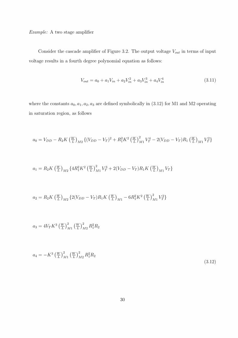
Example: A two stage amplifier
Consider the cascade amplifier of Figure 3.2. The output voltage Vout in terms of input
voltage results in a fourth degree polynomial equation as follows:
Vout = a0 + a1Vin + a2V2in + a3V
3in + a4V
4in (3.11)
where the constants a0, a1, a2, a3 are defined symbolically in (3.12) for M1 and M2 operating
in saturation region, as follows
a0 = VDD −R2K(WL
)M2
(VDD − VT )2 +R2
1K2(WL
)2M1
V 4T − 2(VDD − VT )R1
(WL
)M1
V 2T
a1 = R2K(WL
)M2
4R21K
2(WL
)2M1
V 3T + 2(VDD − VT )R1K
(WL
)M1
VT
a2 = R2K(WL
)M2
2(VDD − VT )R1K(WL
)M1
− 6R21K
2(WL
)2M1
V 2T
a3 = 4VTK3(WL
)2M1
(WL
)2M2
R21R2
a4 = −K3(WL
)2M1
(WL
)2M2
R21R2
(3.12)
30

Nominal values of VDD = 1.2V, VT = 400mV,(WL
)M1
= 12
(WL
)M2
= 20, andK = 100µA/V 2
are substituted to get coefficients in terms of parameters R1 and R2 as given by,
a0 = 1.2−R2(2.56× 10⁻³ + 1.024× 10⁻⁷R21 − 5.12× 10⁻⁴R1
a1 = 4.096× 10⁻⁹R21R2 + 5.12× 10⁻⁶R1R2
a2 = 1.28 × 10⁻⁵R1R2 − 1.536× 10⁻⁸R21R2
a3 = 2.56 × 10⁻⁸R21R2
a4 = 1.6 × 10⁻⁸R21R2
(3.13)
To find the limiting values of the coefficient a0 we assume the parameters R1 and R2
deviate by fractions x and y from their nominal values, respectively. Maximizing a0 we have
the objective function as given by (3.14), subject to constraints 3.15 through 3.19. Note that
here we have set out to find MSDF of R1. Similar approach can be used to find the MSDF
of R2:
1.2−R2,nom(1 + y)2.56× 10⁻³ + 1.024× 10⁻⁷R21,nom(1 + x)2 − 5.12× 10⁻⁴R1,nom(1 + x)
(3.14)
4.096 × 10⁻⁹R21,nom(1 + x)2R2,nom (1 + y)
+5.12 × 10⁻⁶R1,nom(1 + x)R2,nom(1 + y)
= 4.096 × 10⁻⁹R21,nom(1 + ρ)2R2,nom
+ 5.12 × 10⁻⁶R1,nom(1 + ρ)R2,nom
(3.15)
31

Table 3.1: MSDF for cascade amplifier of Figure 3.2 with α = 0.05.
Circuit %upside %downsideparameter MSDF MSDF
Resistor R1 10.3 7.4Resistor R2 12.3 8.5
1.28 × 10⁻⁵R1,nom(1 + x)R2,nom(1 + y)
−1.536× 10⁻⁸R21,nom(1 + x)2R2,nom (1 + y)
= 1.28 × 10⁻⁵R1,nom(1 + ρ)R2,nom
− 1.536 × 10⁻⁸R21,nom(1 + ρ)2R2,nom
(3.16)
2.56× 10⁻⁸R21,nom(1 + x)2R2,nom(1 + y)
= 2.56× 10⁻⁸R21,nom(1 + ρ)2R2,nom
(3.17)
1.6× 10⁻⁸R21,nom(1 + x)2R2,nom(1 + y)
= 1.6× 10⁻⁸R21,nom(1 + ρ)2R2,nom
(3.18)
−α ≤ x, y ≤ α (3.19)
The extreme values for x and y on solving the set of equations 3.15 through 3.19 are obtained
as, x = −α and y = −α, and this gives us the MSDF value for R1, as ρ,
ρ = (1− α)1.5 − 1 ≈ 1.5α− 0.375α2 (3.20)
Table 3.1 gives the MSDF for R1 and R2 based on above calculation.
3.4 Generalization
In general, the calculation as described above cannot be done for an arbitrarily large
circuit. Such circuits are handled by obtaining a nominal numeric polynomial expansion of
the fault free circuit. This is done by sweeping the input voltage across all possible values and
32
noting the corresponding output voltages using any of the standard circuit simulators like
SPICE [4, 98]. Now, the output voltage is plotted against the input voltage. A polynomial
is fitted to this curve and the coefficients of this polynomial are taken to be the nominal
coefficients of the desired polynomial. The circuit is simulated for different drifts in the
parameter values at equally spaced points from inside the hypercube enclosing each circuit
parameter, spaced at a suitably chosen resolution (ϵ). Polynomial coefficients are obtained
for each of these simulations. The maximum and the minimum values of a coefficient in
this search are taken as the limiting values on that coefficient. This process of modeling the
circuit as a polynomial expansion and obtaining limit values on coefficients is repeated at
“key” frequencies of interest. For example, the cut-off frequency in case of a non-linear filter
can be a good candidate for such characterization. Once the limit values on all coefficients
have been determined the CUT is subjected to full range of input at DC and each of the
“key” frequencies. Its response to input sweep is curve fitted to a polynomial of order same
as the fault free circuit. If there are any coefficients that lay outside the limit values of
corresponding coefficients of the fault free circuit, we can conclude the CUT is faulty. The
converse is also true with a high probability that is inversely proportional to coefficient of
uncertainty ϵ. Flow chart in Figure 3.3 summarizes the process of numerically finding the
polynomial and finding the bounds on coefficients. Flow chart in Figure 3.4 outlines the
procedure to test CUT using the described method.
3.5 Experimental Results
Example 1: An Elliptic Filter. We subjected an elliptic filter shown in Figure 3.5 to
Polynomial Coefficient based test. The circuit parameter values are as in the benchmark
circuit maintained by Stroud et al. [70]. We simulated the circuit at four different frequencies.
Two of them were chosen close to its 3dB cut-off frequency (fc), which is 1000Hz. The
estimated polynomial expansions obtained by curve fitting the I/O plots at DC and the
frequencies f = 100Hz, 900Hz, 1000Hz and 1100Hz are given in 3.21 through 3.25 and
33
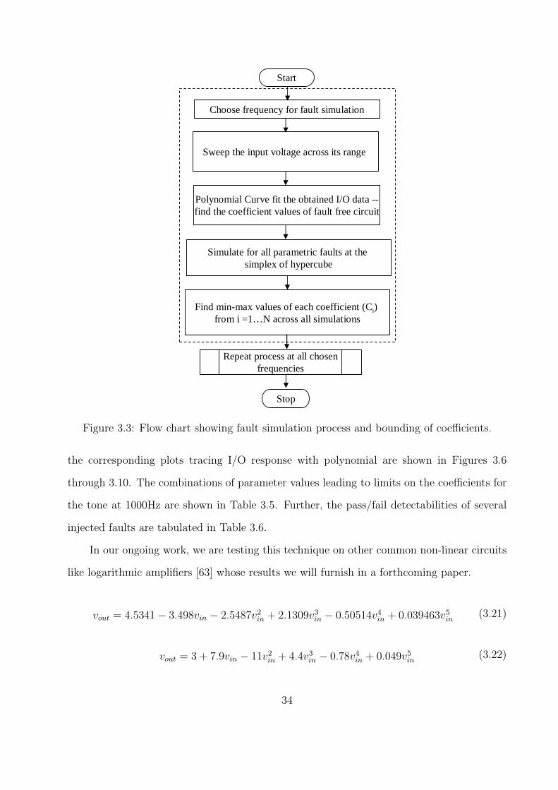
Start
Stop
Find min-max values of each coefficient (Ci) from i =1…N across all simulations
Simulate for all parametric faults at the simplex of hypercube
Choose frequency for fault simulation
Polynomial Curve fit the obtained I/O data --find the coefficient values of fault free circuit
Sweep the input voltage across its range
Repeat process at all chosen frequencies
Figure 3.3: Flow chart showing fault simulation process and bounding of coefficients.
the corresponding plots tracing I/O response with polynomial are shown in Figures 3.6
through 3.10. The combinations of parameter values leading to limits on the coefficients for
the tone at 1000Hz are shown in Table 3.5. Further, the pass/fail detectabilities of several
injected faults are tabulated in Table 3.6.
In our ongoing work, we are testing this technique on other common non-linear circuits
like logarithmic amplifiers [63] whose results we will furnish in a forthcoming paper.
vout = 4.5341− 3.498vin − 2.5487v2in + 2.1309v3in − 0.50514v4in + 0.039463v5in (3.21)
vout = 3 + 7.9vin − 11v2in + 4.4v3in − 0.78v4in + 0.049v5in (3.22)
34
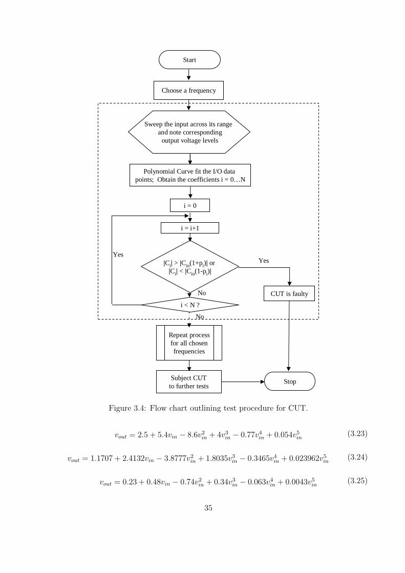
Start
Sweep the input across its range and note correspondingoutput voltage levels
|Ci| > |Cin(1+pi)| or |Ci| < |Cin(1-pi)|
i = 0
i = i+1
i < N ?
Subject CUTto further tests
CUT is faulty
No
Yes
No
Yes
Stop
Repeat process for all chosen frequencies
Choose a frequency
Polynomial Curve fit the I/O data points; Obtain the coefficients i = 0…N
Figure 3.4: Flow chart outlining test procedure for CUT.
vout = 2.5 + 5.4vin − 8.6v2in + 4v3in − 0.77v4in + 0.054v5in (3.23)
vout = 1.1707 + 2.4132vin − 3.8777v2in + 1.8035v3in − 0.3465v4in + 0.023962v5in (3.24)
vout = 0.23 + 0.48vin − 0.74v2in + 0.34v3in − 0.063v4in + 0.0043v5in (3.25)
35

−
+−
+−
+Vout
VinR1
R2
R4
R5
R3 R7
R6
R8
R9
R10
R11 R12
R13
R14
R15
C1
C3
C4
C5
C6 C7
C2
Figure 3.5: Elliptic filter.
Example 2: Low Noise Amplifier (LNA). We simulated a Low noise amplifier shown in
Figure 3.12 for polynomial coefficient based test. Notice that the bias current Ibias shown
in the figure is derived from a current mirror powered by band-gap reference circuitry (not
shown). The circuit parameter values were chosen to meet performance specifications tab-
ulated in Table 3.2. We used parametric faults of sizes α = 5% from their nominal value
to find min-max values of coefficients. Figure 3.13 shows the simulated response at four
different frequencies, namely, f = 1GHz, 10GHz, 15GHz, and 35GHz and the estimated
polynomials obtained by curve fitting a fifth order polynomial are given by equations (3.26)
through (3.29), respectively. To obtain these curves, input offset voltage is varied from 0
through 5V as shown (on X-axis), while measuring the output voltage magnitude at each
of these input voltage points. As we can see in the figure (on the far right), the output
magnitude at 35GHz, drops to about 72% its value at preceding three frequencies, which
36

0 1 2 3 4 5−3
−2
−1
0
1
2
3
4
5
Input DC voltage (Vin)
Out
put V
olta
ge(V
out)
Simulated
5th degree polynomial
a5 = 0.039463a4 = −0.50514a3 = 2.1309a2 = −2.5487a1 = −3.498a0 = 4.5341
Figure 3.6: DC response of elliptic filter with curve fitting polynomial.
0 0.5 1 1.5 2 2.5 3 3.5 4 4.5 5−1
0
1
2
3
4
5
Input Voltage, Vin(v)
Out
put V
olta
ge, V
out(
v)
a5 = 0.049 a4 = − 0.78 a3 = 4.4 a2 = − 11 a1 = 7.9 a0 = 3
Simulated
5th degree Polynomial
Figure 3.7: Curve-fit polynomial with coefficients at frequency = 100Hz.
37

0 1 2 3 4 5−2
−1
0
1
2
3
4
5
Input Voltage, Vin(v)
Out
put V
olta
ge, V
out(
v)
a5 = 0.054 a4 = − 0.77 a3 = 4 a2 = − 8.6 a1 = 5.4 a0 = 2.5
Simulated 5th degree Polynomial
Figure 3.8: Curve-fitting polynomial with coefficients at frequency = 900Hz.
0 0.5 1 1.5 2 2.5 3 3.5 4 4.5 5−0.2
0
0.2
0.4
0.6
0.8
1
1.2
1.4
1.6
1.8
Input Voltage, Vin(v)
Out
put V
olag
e, V
out(
v)
Simulated
5th degree Polynomial
a5 = 0.024a4 = −0.35a3 = 1.8a2 = −3.9a1 = 2.4a0 = 1.2
Figure 3.9: Curve-fitting polynomial with coefficients at frequency = 1000Hz.
38

0 0.5 1 1.5 2 2.5 3 3.5 4 4.5 5−0.2
0
0.2
0.4
0.6
0.8
1
1.2
1.4
Input Voltage, Vin(v)
Out
put V
olta
ge, V
out(
v)
a5 = 0.0043 a4 = − 0.063 a3 = 0.34 a2 = − 0.74 a1 = 0.48 a0 = 0.23
Simulated
5th degree Polynomial
Figure 3.10: Curve-fitting polynomial with coefficients at frequency = 1100Hz.
p1
p2
p3
...
pk
C1
C2
C3
.
.
Ci
.
Cn
1
1
CpS
1
k
CpS
n
k
CpS
2
2
CpS
3
k
CpS
Parameter space
Coefficient space
Figure 3.11: Mapping showing one possible relation between various parameters and coeffi-cients.
39

Figure 3.12: Low noise amplifier (LNA) schematic.
Table 3.2: LNA specification.Performance Parameter Nominal Value
Gain (dB) 16IIP3 (dBm) -18
Noise figure (dB) 9.1S11 (dB) -16.5
confirms (in close neighborhood of) 35GHz as the 3dB cut-off, and thereby the ultra-wide
bandwidth LNA designed and tested in this example.
Figure 3.14 compares the I/O response of the LNA for three different value of the load
resistance RL.
vout =(2.5− 1.498vin − 1.2688v2in + 1.139v3in − 0.88514v4in + 0.039463v5in
)× 10−3 (3.26)
vout =(2.36− 1.348vin − 1.3268v2in + 1.049v3in − 0.63614v4in + 0.04443v5in
)× 10−3 (3.27)
vout =(2.12− 1.267vin − 1.1285v2in − 1.016v3in + 0.88516v4in − 0.052876v5in
)× 10−3 (3.28)
vout =(1.95− 1.068vin + .9268v2in + .786v3in − 0.77324v4in + 0.042v5in
)× 10−3 (3.29)
40
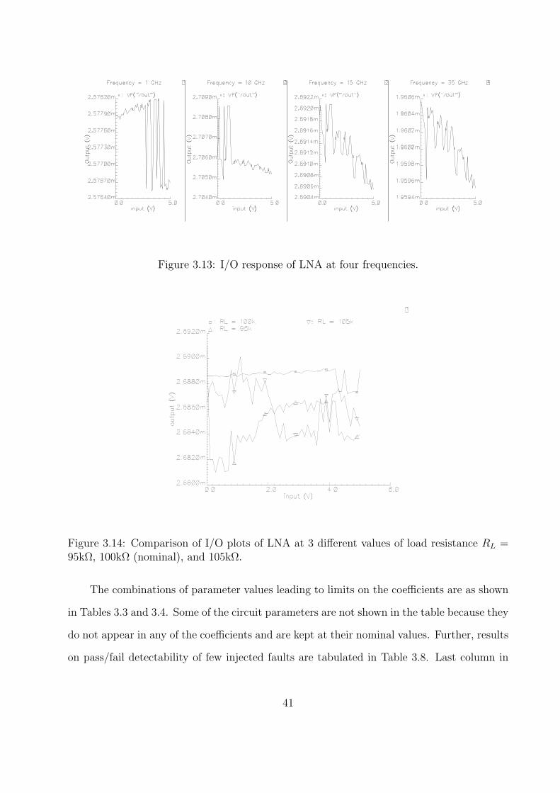
Figure 3.13: I/O response of LNA at four frequencies.
Figure 3.14: Comparison of I/O plots of LNA at 3 different values of load resistance RL =95kΩ, 100kΩ (nominal), and 105kΩ.
The combinations of parameter values leading to limits on the coefficients are as shown
in Tables 3.3 and 3.4. Some of the circuit parameters are not shown in the table because they
do not appear in any of the coefficients and are kept at their nominal values. Further, results
on pass/fail detectability of few injected faults are tabulated in Table 3.8. Last column in
41
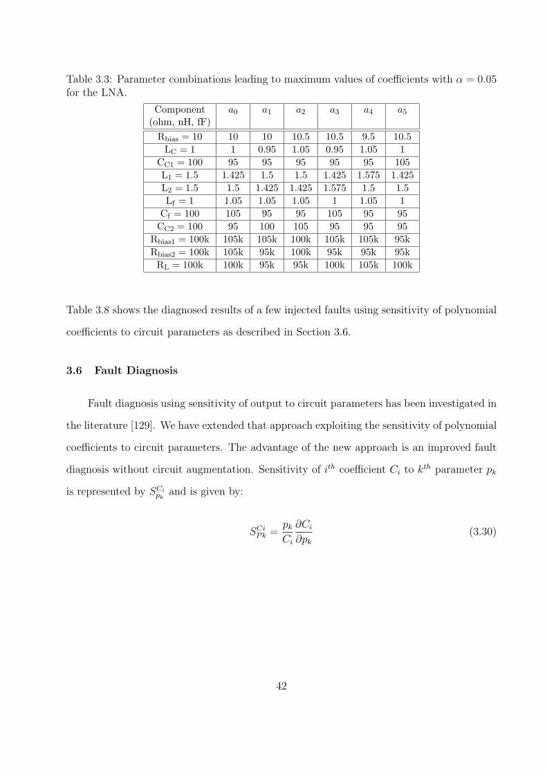
Table 3.3: Parameter combinations leading to maximum values of coefficients with α = 0.05for the LNA.
Component a0 a1 a2 a3 a4 a5(ohm, nH, fF)
Rbias = 10 10 10 10.5 10.5 9.5 10.5
LC = 1 1 0.95 1.05 0.95 1.05 1
CC1 = 100 95 95 95 95 95 105
L1 = 1.5 1.425 1.5 1.5 1.425 1.575 1.425
L2 = 1.5 1.5 1.425 1.425 1.575 1.5 1.5
Lf = 1 1.05 1.05 1.05 1 1.05 1
Cf = 100 105 95 95 105 95 95
CC2 = 100 95 100 105 95 95 95
Rbias1 = 100k 105k 105k 100k 105k 105k 95k
Rbias2 = 100k 105k 95k 100k 95k 95k 95k
RL = 100k 100k 95k 95k 100k 105k 100k
Table 3.8 shows the diagnosed results of a few injected faults using sensitivity of polynomial
coefficients to circuit parameters as described in Section 3.6.
3.6 Fault Diagnosis
Fault diagnosis using sensitivity of output to circuit parameters has been investigated in
the literature [129]. We have extended that approach exploiting the sensitivity of polynomial
coefficients to circuit parameters. The advantage of the new approach is an improved fault
diagnosis without circuit augmentation. Sensitivity of ith coefficient Ci to kth parameter pk
is represented by SCipk
and is given by:
SCiPk =
pkCi
∂Ci
∂pk(3.30)
42

Table 3.4: Parameter combinations leading to Min values of coefficients with α = 0.05 forthe LNA.
Component a0 a1 a2 a3 a4 a5(ohm, nH, fF)
Rbias = 10 10 9.5 9.5 10 10 10
LC = 1 1.05 0.95 0.95 1 1 0.95
CC1 = 100 100 105 95 100 95 105
L1 = 1.5 1.425 1.5 1.575 1.575 1.575 1.575
L2 = 1.5 1.5 1.575 1.5 1.425 1.425 1.5
Lf = 1 1.05 1.05 0.95 0.95 1 0.95
Cf = 100 105 95 95 105 105 105
CC2 = 100 95 105 100 105 95 105
Rbias1 = 100k 100k 95k 105k 105k 95k 100k
Rbias2 = 100k 100k 105k 95k 95k 105k 95k
RL = 100k 95k 100k 95k 100k 105k 95k
3.6.1 Computation of Sensitivities
Numerical computation of sensitivities given by (3.30) is accomplished by introducing
fractional drifts (=α) in each component (pk ∀k); simulating the circuit and measuring the
fractional drift in each coefficient of the polynomial resulting from curve fitting operation.
This way the numerical sensitivities are computed and a dictionary is maintained for sensi-
tivities. The complexity in computation of sensitivities is linear in the number N of circuit
parameters, i.e., O(N).
3.6.2 Diagnosing Parametric Faults
Restricting ourselves to single parametric faults, we find the descending order of sensi-
tivities of coefficients (with respect to circuit parameter) that have exceeded their limiting
values. The parameter with highest sensitivity is said to be at fault with a probability
P(δpk|δCi) (which can be interpreted as the confidence in diagnosing fault), given by (3.31),
where δpk is the suspected drift in parameter pk and δCi is the measured drift in coefficient.
P(δpk|δCi) =SCiPkδpkδCi
(3.31)
43
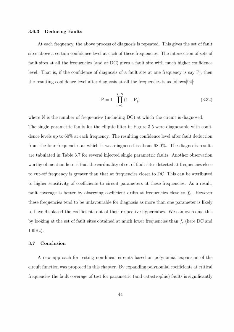
3.6.3 Deducing Faults
At each frequency, the above process of diagnosis is repeated. This gives the set of fault
sites above a certain confidence level at each of these frequencies. The intersection of sets of
fault sites at all the frequencies (and at DC) gives a fault site with much higher confidence
level. That is, if the confidence of diagnosis of a fault site at one frequency is say Pi, then
the resulting confidence level after diagnosis at all the frequencies is as follows[94]:
P = 1−i=N∏i=1
(1− Pi) (3.32)
where N is the number of frequencies (including DC) at which the circuit is diagnosed.
The single parametric faults for the elliptic filter in Figure 3.5 were diagnosable with confi-
dence levels up to 60% at each frequency. The resulting confidence level after fault deduction
from the four frequencies at which it was diagnosed is about 98.9%. The diagnosis results
are tabulated in Table 3.7 for several injected single parametric faults. Another observation
worthy of mention here is that the cardinality of set of fault sites detected at frequencies close
to cut-off frequency is greater than that at frequencies closer to DC. This can be attributed
to higher sensitivity of coefficients to circuit parameters at these frequencies. As a result,
fault coverage is better by observing coefficient drifts at frequencies close to fc. However
these frequencies tend to be unfavourable for diagnosis as more than one parameter is likely
to have displaced the coefficients out of their respective hypercubes. We can overcome this
by looking at the set of fault sites obtained at much lower frequencies than fc (here DC and
100Hz).
3.7 Conclusion
A new approach for testing non-linear circuits based on polynomial expansion of the
circuit function was proposed in this chapter. By expanding polynomial coefficients at critical
frequencies the fault coverage of test for parametric (and catastrophic) faults is significantly
44

Table 3.5: Parameter combinations leading to Max and Min Values of coefficients withα = 0.05 at 1000Hz for the elliptic filter.
Circuit Parameters (Resistance in Ω,Capacitance in Farad)Nominal Maximum values Minimum valuesValues a0 a1 a2 a3 a4 a5 a0 a1 a2 a3 a4 a5
R1 = 19.6k 18.6k 18.6k 20.5k 20.5k 20.5k 18.6k 18.6k 18.6k 18.6k 18.6k 20.5k 20.5kR2 = 196k 205k 205k 205k 205k 186k 186k 205k 186k 186k 205k 205k 205kR3 = 147k 139k 139k 154k 139k 139k 139k 139k 139k 154k 139k 139k 139kR4 = 1k 950 950 1.05k 1.05k 1.05k 1.05k 1.05k 950 1.05k 950 950 1.05kR5 = 71.5 75 67 75 67 67 75 75 75 67 67 75 67R6 = 37.4k 35k 39k 39k 35k 35k 39k 39k 39k 35k 35k 35k 35kR7 = 154k 146k 146k 161k 161k 146k 146k 146k 146k 161k 161k 146k 146kR8 = 260 247 273 273 247 247 273 273 247 273 247 273 247R9 = 740 703 777 703 703 777 703 703 703 777 703 703 703R10 = 500 475 525 525 475 525 525 475 525 475 475 525 475R11 = 110k 115k 115k 115k 104k 104k 104k 115k 115k 104k 115k 104k 104kR12 = 110k 104k 104k 115k 115k 115k 115k 115k 115k 104k 104k 115k 104kR13 = 27.4k 28.7k 26k 26k 26k 28.7k 28.7k 26k 26k 28.7k 26k 28.7k 26kR14 = 40 42 38 42 38 38 42 42 38 42 42 38 42R15 = 960 912 912 912 912 912 1k 1k 1k 912 1k 912 912C1 = 2.67n 2.5n 2.5n 2.5n 2.5n 2.5n 2.5n 2.8n 2.5n 2.8n 2.8n 2.8n 2.5nC2 = 2.67n 2.5n 2.8n 2.8n 2.5n 2.8n 2.8n 2.8n 2.8n 2.5n 2.8n 2.5n 2.8nC3 = 2.67n 2.8n 2.8n 2.8n 2.5n 2.8n 2.8n 2.8n 2.8n 2.8n 2.5n 2.8n 2.8nC4 = 2.67n 2.5n 2.8n 2.5n 2.5n 2.5n 2.5n 2.5n 2.5n 2.8n 2.5n 2.5n 2.8nC5 = 2.67n 2.5n 2.5n 2.5n 2.5n 2.5n 2.8n 2.8n 2.8n 2.8n 2.8n 2.8n 2.8nC6 = 2.67n 2.5n 2.8n 2.5n 2.8n 2.5n 2.8n 2.5n 2.5n 2.8n 2.8n 2.8n 2.5nC7 = 2.67n 2.5n 2.8n 2.8n 2.8n 2.8n 2.5n 2.8n 2.5n 2.5n 2.5n 2.5n 2.8n
improved, yielding a minimum size of detectable faults in some circuit components as low as
5%. The method has been extended to sensitivity based fault diagnosis with probabilistic
confidence levels in parameter drifts. Further the expansion at multiple tones leads to a
higher confidence level (up to 98.9%) in diagnosing single parametric fault sites. In the next
chapter, we shall discuss the use of V-transform for further enhancing the fault detection
capabilities of the polynomial coefficients.
45
Table 3.6: Results of some injected faults at different frequencies for the elliptic filter.
Injected Coefficients out of Bounds at Detectedfault DC f1=100Hz f2=900Hz f3=1000Hz f4=1100Hz
R1 down 15% a0 − a4 a1 − a4 a3, a5 a2, a4 a1, a2 Yes
R2 down 5% a2, a5 a1, a3 a1, a5 a1, a2, a5 a1, a2 Yes
R3 up 10% a1, a2, a3 a3, a5 a0, a3, a4 a1, a3, a4 a1, a5 Yes
R4 down 20% a0 − a3 a1 − a2 a2, a3 a1, a2, a3 a2, a3 Yes
R5 up 15% a0, a5 a1 a0, a2 a0, a2, a3 a3 Yes
R6 up 5% − a1, a2 a2, a3, a5 a1, a3 a1 Yes
R7 down 10% a2, a4 a3, a5 a0, a1, a2 a1, a4, a5 a2, a3 Yes
R8 up 10% − a2 a0, a4 a0, a2, a5 a3, a4 Yes
R9 down 5% − a3, a2 a1, a2, a4 a2, a3, a5 a1, a3 Yes
R10 up 15% − a1, a4 a1, a3, a4 a0, a1, a4 a1, a2 Yes
R11 down 10% a0, a2 a3, a4 a0, a1 a1, a2, a4 a1, a2 Yes
R12 down 15% a0, a4 a1, a3 a1, a2, a3 a1, a2 a2, a5 Yes
R13 up 5% − a3, a5 a1, a2 a1, a2, a4 a0, a2 Yes
R14 up 20% − a1, a3 a0, a3, a4 a0, a1, a2 a3, a4 Yes
R15 up 5% − a4 a3, a5 a0, a1, a3 a0, a5 Yes
C1 down 10% − a4, a5 a4, a5 a1, a2, a3 a1, a4 Yes
C2 up 10% − a2, a3 a1, a2 a2, a3, a4 a0, a4 Yes
C3 down 15% − a1, a3 a0, a1, a2 a4, a5 a0, a1 Yes
C4 down 10% − a0, a1 a1, a2 a2, a3 a2, a5 Yes
C5 up 5% − a0, a1 a1, a5 a1, a2 a3, a4 Yes
C6 up 15% − a3, a4 a1, a2, a4 a3, a4, a5 a1, a2 Yes
C7 up 15% − a1, a4 a1, a3, a4 a1, a3, a5 a3, a4 Yes
46

Table 3.7: Parametric fault fiagnosis with confidence levels of ≈ 98.9% for the elliptic filter.
Injected fault Diagnosed fault sites at DeducedDC 100Hz 900Hz 1000Hz 1100Hz fault site
R1 down 15% R1,R4 R1 R1,R2 R1,R2,C1 R1,C1 R1
R2 down 5% R2 R2,C1 R2,R3,C1 R2,R3 R2,C1 R2
R3 up 10% R1,R3 R3,C3 R3,R4,C3 R3 R3,C3 R3
R4 down 20% R1,R4 R1,R4 R2,R4,C1 R1,R2,R4 R1,R2,R4 R4
R5 up 15% R5 R5,C2 R4,R5 R4,R5,C2 R5,R6,C3 R5
R6 up 5% − R6,C2 R6,R7 R6,C2,C4 R6,C2,C3 R6
R7 down 10% R3,R7 R7,C3 R3,R7 R3,R6,R7 R3,R7,C3 R7
R8 up 10% − R6,R8 R8,R9 R6,R8 R8,R9 R8
R9 down 5% − R8,R9 R8,R9 R9,R10 R8,R9 R9
R10 up 15% − R10 R10,C6 R10 R10,C6 R10
R11 down 10% R11,R12 R11 R11,C5 R11,R12 R11,R12,C5 R11
R12 down 15% R11,R12 R11,R12 R12,C5 R12,C5 R12,C5,C7 R12
R13 up 5% − R13,C5 R13,C7 R13,C5,C6 R13,C5 R13
R14 up 20% − R14 R14,R15 R14,R15 R14,R15 R14
R15 up 5% − R13,R15 R14,R15 R14,R15,C5 R14,R15 R15
C1 down 10% − R2,C1 R2,C1 R2,C1 R2,C1 C1
C2 up 10% − R5,C2 C2,C4 C2 C2 C2
C3 down 15% − C3 R3,C3 C3 C3 C3
C4 down 10% − R6,C4 C2,C4 C2,C4 C2,C4 C4
C5 up 5% − C5 R12,C5 C5 C5 C5
C6 up 15% − R10,C6 C6,C7 C6,C7 C6,C7 C6
C7 up 15% − C6,C7 C7 C6,C7 C6,C7 C7
Table 3.8: Results of test and diagnosis of some injected faults for LNA.
Circuit Parameter Coefficients that are Detected Diagnosedout of bounds fault sites
Rbias down 25% a0 − a4 Yes Rbias
LC down 15% a2, a5 Yes LC or CC1
CC1 up 10% a1, a2, a3 Yes CC1 or LC
L1 down 25% a0 − a4 Yes L1
L2 up 15% a0, a4 Yes L2
Lf up 10% a1, a2 Yes Lf or Cf
Cf up 10% a4, a5 Yes Lf
CC2 down 10% a4, a5 Yes CC2
47

Chapter 4
V-Transform Coefficients as Test Signatures
4.1 Introduction
Non-linear circuit testing has been well studied and different methods have been pro-
posed for finding parametric faults [6, 35, 37, 40, 44, 52, 75, 99]. Prominent among them in
the industry is the IDDQ based testing where current from the supply rail is monitored and
sizable deviation from its quiescent value is reported. However, this requires augmentation
of the CUT. For example, in the simplest case a regulator supplying power to any sizable
circuit has to be augmented with a current sensing resistor and an ADC (for digital output)
and then there is subsequent analysis to be performed on sensed current. Further IDDQ is
suitable only for catastrophic faults as the current drawn from the supply is distinguishable
only when there is some “big enough” fault so as to change the current drawn from the
supply from its quiescent value to a region where it is distinguishable. For example with
resistor R2 being open in Figure 4.1, the current drawn from supply can change by 50% of
its quiescent value. Such faults can typically be found by monitoring IDDQ using a current
sensor. However parametric deviations say lesser than 10% from its nominal value cannot
be observed using this scheme, specially so in the deep submicron era where the leakage
currents can be comparable with defect induced current [45]. The other approach for testing
parametric faults that can be found in literature [65, 67, 134, 135, 137] is based on the use of
neural networks. Neural network based approaches propose the use of circuit observer blocks
to track the output for a set of input signals which is used for training the neurons. The
trained set of neurons is then used to estimate variations in the output for a standard input
stimulus. This method, however, suffers from large amounts of training required and the
consequent increase in test application time that the scheme is prohibitive for even medium
48
sized analog circuits at production. More recently, the use of Volterra series coefficients was
proposed to estimate non-linear characteristics of the system. These coefficients are then
used for testing the circuit with a pseudo random input stimulus [95, 96]. This method
however suffers from the high computational requirement of estimation of Volterra series
coeffcients for every circuit at production which can increase the test cost significantly. It
is therefore interesting to develop a method to detect parametric faults with little circuit
augmentation while keeping the test access mechanism simple and the test application time
to a minimum.
To address the issue of parametric deviation, we would typically need more observables
to have an idea about the parametric drift in circuit parameters. This would mean an increase
in complexity of the sensing circuit. However, we would also want only little augmentation
to tap any of the internal circuit nodes or currents. To overcome these seemingly contrasting
requirements the method intended should have some way of “seeing through” the circuit
with only the outputs and inputs at its disposal. References [53, 93] have accomplished this
sort of a strategy for linear circuits in a different context as described next.
Guo and Savir [53] describe a method based on transfer function of a circuit under test
(CUT). The transfer function, H(s), of the CUT is expressed as:
H(s) =
M∑i=0
aisi
N∑i=0
bisi(M < N) (4.1)
Here, ai and bi are referred to as transfer function coefficients (TFCs). The CUT is subjected
to frequency rich input signals and the output at these frequencies is observed. With these
input-output pairs they estimate the TFCs of CUT. These coefficients are now compared
with the ideal circuit TFCs, which are known a priori. The CUT is classified faulty if any
of the estimated coefficients are beyond the tolerable range. This method necessarily needs
the CUT to be linear, as transfer functions are possible only for LTI systems.
49
To extend the above idea to more general non-linear circuits we adopted a strategy
in [122, 125, 126] where we expand the function of the circuit as a polynomial by the Taylor’s
series expansion about the input voltage mangitude vin at a given frequency, as follows:
vout = f(vin) = f(0) + f ′(0)1!vin +
f ′′(0)2!v2in +
f ′′′(0)3!
v3in+
· · ·+ f (n)(0)n!
vnin + · · ·(4.2)
where f(vin) is a real function of vin. Ignoring the higher order terms in (4.2), we can expand
vout up to the nth power of vin, which gives us the approximation in (4.3):
vout = a0 + a1vin + a2v2in + · · ·+ anv
nin (4.3)
where a0, a1, a2, . . . , an are all real-valued functions of circuit parameters pk, ∀k. Further
assume that normal parameter variations (normal drift) in a good circuit are within a frac-
tion α of their nominal value, where α << 1. This means that every parameter pi is allowed
to vary within the range pk,nom(1 − α) < pk < pk,nom(1 + α), ∀k, where pk,nom is the nom-
inal value of parameter pk. Whenever one or more of the coefficient values slip outside its
individual hypercube we get a different set of coefficients that reflects a detectable fault.
Therefore, equation (4.4) describes a hypercube for all parameters that correspond to either
good machine values or undetectable parameter faults [35, 53, 99]:
ai,min < ai < ai,max ∀ai, 0 ≤ i ≤ n (4.4)
In the latter portion of this chapter we address an important problem that has kept
analog circuit test cost high [86], namely, distinguishing between faults induced due to process
variation. For example, we would like to distinguish random drifts in tox, W , L, and doping
densities of devices in an integrated circuits from those resulting from manufacturing defect
induced (parametric) faults (e.g., Lithographic errors, etching errors, etc.) that lead to a
substantial deviation of a circuit from its nominal behavior but are not large enough to render
the circuit dysfunctional. We quantify an error distance measure between faults induced due
50

to process variation with those induced due to manufacturing defects. We can then estimate
the probabilities of a detected fault being caused by process variation or by a manufacturing
defect. We make this estimation based on maximizing a posteriori probabilities of the two
kinds of errors conditioned on the event that a fault is detected.
Most of the material in this chapter is taken from recently published papers [118, 119]
by the author. This chapter is organized as follows. Section 4.2 we state previously pub-
lished results [124] on the polynomial expansion of function f(vin) and notions of detectable
fault sizes. Section 4.3 outlines V-transform and the resulting sensitivity improvement. In
Section 4.4 we describe the problem at hand and discuss the proposed solution with an
example. In Section 4.5 we generalize the test solution to an arbitrarily large circuit. Sec-
tion 4.6 establishes, 1) a method to distinguish between process variation induced faults and
those induced due to manufacturing defects and 2) identify the fault site if it is of the latter
kind. Section 4.7 presents the simulation results for a standard elliptic filter. We conclude
in Section 4.9.
4.2 Background
The coefficients ai, ∀0 ≤ i ≤ n, are in general non-linear functions of circuit parameters
pk, ∀k. The rationale in using these coefficients as metrics in classifying CUT as faulty or
fault free is based on the premise of dependence of coefficients on circuit parameters.
Theorem 4.1 If coefficient ai is a monotonic function of all parameters, then ai takes its
limit (maximum and minimum) values when at least one or more of the parameters are at
the boundaries of their individual hypercube.
Lemma 2 If coefficient ai is a non-monotonic function of one or more circuit parameters
pi, then ai can take its limit values anywhere inside the hypercube enclosing the parameters.
By Theorem 4.1 and Lemma 2 it is clear that by exhaustively searching the space in the
hypercube of each parameter we can get the maximum and minimum values of the polynomial
51
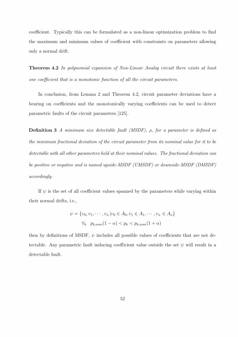
coefficient. Typically this can be formulated as a non-linear optimization problem to find
the maximum and minimum values of coefficient with constraints on parameters allowing
only a normal drift.
Theorem 4.2 In polynomial expansion of Non-Linear Analog circuit there exists at least
one coefficient that is a monotonic function of all the circuit parameters.
In conclusion, from Lemma 2 and Theorem 4.2, circuit parameter deviations have a
bearing on coefficients and the monotonically varying coefficients can be used to detect
parametric faults of the circuit parameters [125].
Definition 3 A minimum size detectable fault (MSDF), ρ, for a parameter is defined as
the minimum fractional deviation of the circuit parameter from its nominal value for it to be
detectable with all other parameters held at their nominal values. The fractional deviation can
be positive or negative and is named upside-MSDF (UMSDF) or downside-MSDF (DMSDF)
accordingly.
If ψ is the set of all coefficient values spanned by the parameters while varying within
their normal drifts, i.e.,
ψ = υ0, υ1, · · · , υn |υ0 ∈ A0, υ1 ∈ A1, · · · , υn ∈ An
∀k pk,nom(1− α) < pk < pk,nom(1 + α)
then by definitions of MSDF, ψ includes all possible values of coefficients that are not de-
tectable. Any parametric fault inducing coefficient value outside the set ψ will result in a
detectable fault.
52

4.3 The V-Transform
We define V-transform coefficients as follows: if C1, C2 · · ·Cn are polynomial coefficients
of CUT then their V-transform coefficients, VC1 , VC2 · · ·VCn , are
VCi= eγC
′i ∀ 0 ≤ i ≤ n (4.5)
where C ′i are the modified polynomial coefficients defined indirectly as follows
dC ′i
dpj=
∣∣∣∣dCi
dpj
∣∣∣∣ ∀ 0 ≤ i ≤ n (4.6)
The modification C ′i according to (4.6) ensures that the modified polynomial coefficients are
monotonic with the polynomial coefficients. Further, the V-transform coefficients (VTC) are
exponential functions of the modified polynomial coefficients and γ is a sensitivity parameter
chosen according to the desired sensitivity. The gain in sensitivity of V-transform coefficients
to circuit parameters over the sensitivity of ordinary polynomial coefficients is given by
SVCipi
SCipi
=
∣∣∣dCi
dpi
∣∣∣ γeγC′i × pi
eγC′i
dCi
dpi× pi
Ci
= γCi (4.7)
Choices of γ = 3, for instance, results in a 3 times more sensitive coefficient to circuit
parameters.
4.4 A Problem and an Approach
We shall first illustrate with an example the calculation of limits of the polynomial
coefficients for a simple circuit using MOS transistors. We shall follow this up with MSDF
values for the circuit parameters.
Example. Two stage amplifier: Consider the cascade amplifier shown in Figure 4.1. The
output voltage Vout in terms of input voltage results in a fourth degree polynomial:
Vout = a0 + a1Vin + a2V2in + a3V
3in + a4V
4in (4.8)
53
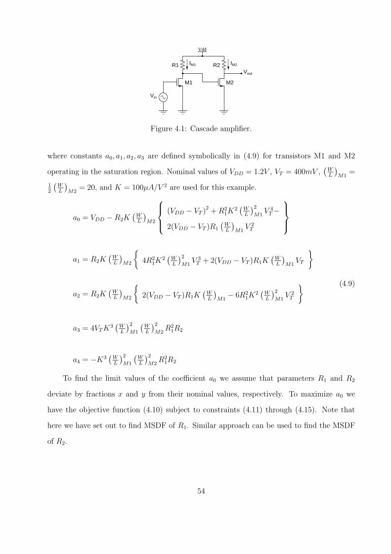
Vdd
R2R1 IM1 IM2
M1 M2
Vin
Vout
Figure 4.1: Cascade amplifier.
where constants a0, a1, a2, a3 are defined symbolically in (4.9) for transistors M1 and M2
operating in the saturation region. Nominal values of VDD = 1.2V , VT = 400mV ,(WL
)M1
=
12
(WL
)M2
= 20, and K = 100µA/V 2 are used for this example.
a0 = VDD −R2K(WL
)M2
(VDD − VT )2 +R2
1K2(WL
)2M1
V 4T−
2(VDD − VT )R1
(WL
)M1
V 2T
a1 = R2K
(WL
)M2
4R2
1K2(WL
)2M1
V 3T + 2(VDD − VT )R1K
(WL
)M1
VT
a2 = R2K(WL
)M2
2(VDD − VT )R1K
(WL
)M1
− 6R21K
2(WL
)2M1
V 2T
a3 = 4VTK3(WL
)2M1
(WL
)2M2
R21R2
a4 = −K3(WL
)2M1
(WL
)2M2
R21R2
(4.9)
To find the limit values of the coefficient a0 we assume that parameters R1 and R2
deviate by fractions x and y from their nominal values, respectively. To maximize a0 we
have the objective function (4.10) subject to constraints (4.11) through (4.15). Note that
here we have set out to find MSDF of R1. Similar approach can be used to find the MSDF
of R2.
54

1.2−R2,nom(1 + y)
2.56× 10⁻³+
1.024 × 10⁻⁷R21,nom(1 + x)2
−5.12 × 10⁻⁴R1,nom(1 + x)
(4.10)
4.096 × 10⁻⁹R21,nom(1 + x)2R2,nom (1 + y)
+5.12 × 10⁻⁶R1,nom(1 + x)R2,nom(1 + y)
= 4.096 × 10⁻⁹R21,nom(1 + ρ)2R2,nom
+ 5.12 × 10⁻⁶R1,nom(1 + ρ)R2,nom
(4.11)
1.28 × 10⁻⁵R1,nom(1 + x)R2,nom(1 + y)
−1.536× 10⁻⁸R21,nom(1 + x)2R2,nom (1 + y)
= 1.28 × 10⁻⁵R1,nom(1 + ρ)R2,nom
− 1.536 × 10⁻⁸R21,nom(1 + ρ)2R2,nom
(4.12)
2.56× 10⁻⁸R21,nom(1 + x)2R2,nom(1 + y)
= 2.56× 10⁻⁸R21,nom(1 + ρ)2R2,nom
(4.13)
1.6× 10⁻⁸R21,nom(1 + x)2R2,nom(1 + y)
= 1.6× 10⁻⁸R21,nom(1 + ρ)2R2,nom
(4.14)
−α ≤ x, y ≤ α (4.15)
The extreme values for x and y are obained by solving the set of equations 4.10 through 4.15.
We get x = −α and y = −α and this gives the MSDF for R1, as
ρ = (1− α)1.5 − 1 ≈ 1.5α− 0.375α2 (4.16)
Table 4.1 gives the MSDF for R1 and R2 based on the above calculation.
55

Table 4.1: MSDF for cascade amplifier of Figure 4.1 with α = 0.05.
Circuit %upside %downsideparameter MSDF MSDF
Resistor R1 10.3 7.4Resistor R2 12.3 8.5
4.5 Generalization
The computation of the previous section is too complex for arbitrarily large circuits.
Such circuits are handled by first obtaining a nominal numeric polynomial expansion for
them. This is done by sweeping the input voltage across all possible values and noting the
corresponding output voltages. The output voltage is plotted against the input voltage. A
polynomial is fitted to this curve and the coefficients of this polynomial are taken to be the
nominal coefficients for the desired polynomial. A V-transform curve is now obtained based
on the polynomial curve using the transformation in equation (4.5).
The circuit is simulated for different drifts in the parameter values at equally spaced
points from inside the hypercube enclosing each circuit parameter, spaced ϵ apart. Polyno-
mial coefficients and hence V-transform coefficients are obtained for each of these simulations.
The maximum and minimum values of coefficient in this search are taken as the limiting val-
ues for that coefficient. Once the limiting values for all coefficients have been determined
the CUT is subjected to a DC sweep at the input and the output response is curve-fitted
using a polynomial of the same order as that used for the fault free circuit. The V-transform
coefficients for CUT are now obtained. If there are any coefficients that lay outside the
limiting values of the corresponding coefficients of the fault free circuit, we conclude that
CUT is faulty. The converse need not be true as there could be other specifications, the
circuit needs to meet, which are not captured by polynomial based test. Flowchart I in Fig-
ure 4.2 summarizes the process of numerically finding the V-transform coefficients and their
bounds. Flowchart II in Figure 4.2 outlines a procedure to test CUT using the V-transform
56
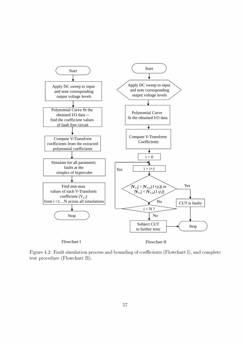
Start
Apply DC sweep to inputand note correspondingoutput voltage levels
Polynomial Curve fit the obtained I/O data --
find the coefficient values of fault free circuit
Compute V-Transform coefficients from the extracted
polynomial coefficients
Start
Compute V-Transform Coefficients
Polynomial Curve fit the obtained I/O data
Apply DC sweep to inputand note correspondingoutput voltage levels
i = 0
Stop
Find min-max values of each V-Transform
coefficient (VCi) from i =1…N across all simulations
Simulate for all parametric faults at the
simplex of hypercube
|VCi| > |VCin(1+ρi)| or |VCi| < |VCin(1-ρi)|
i = 0
i = i+1
i < N ?
Subject CUTto further tests
CUT is faulty
No
Yes
No
Yes
Stop
Flowchart I Flowchart II
Figure 4.2: Fault simulation process and bounding of coefficients (Flowchart I), and completetest procedure (Flowchart II).
57

coefficients. The bounds on coefficients of fault free circuit are found a priori as shown in
Flowchart I of Figure 4.2.
4.6 Fault Diagnosis
Fault diagnosis involves the location of likely fault sites in a CUT given that the CUT has
failed an applied test giving a particular response. We use V-transform coefficients (VTC) to
characterize the response of the circuit at different frequencies (about 4 or 5 frequencies are
sufficient for most circuits with less than 100 circuit elements), by obtaining its input-output
response over the entire input range. Process variation induces a fault-free variation of say σ,
about the mean value of every VTC. Any value beyond σ from the mean µ of VTC indicates
a circuit failure. Assuming a normal distribution for circuit parameter variation, we can
find the probability distribution of the coefficients by Monte-Carlo simulation for process
variation of all circuit parameters. Once the Monte-Carlo distributions for the coefficients of
fault free circuit are obtained we can inject desired sizes of parametric faults (those that are
induced due to manufacturing defects) and obtain the new probability distribution of faulty
circuit under process variation.
As an illustration, Figure 4.3 shows the probability density distributions obtained with
(broken line) and without (solid line) parametric fault. There are three distinct regions in the
probability space of any coefficient Ck. Region R is the fault-free space because coefficients
at all frequencies are within the desired limits. Region 1 where dominant mechanism of faults
are due to PV of circuit parameters and Region 2 where dominant mechanism of faults is due
to manufacturing defects (also called parametric fault). The cross-over point of these two
distributions gives the equiprobable region of faults, where we can have faults due to either
of the mechanism with the same likelihood. We denote this point on the coefficient axis as
Cth. Measuring the value of coefficient C of CUT, we can now determine the likelihood of the
nature of fault mechanism. That is, C ∈ [µ,Cth] =⇒ failures due to PV are more in number
and C ∈ [Cth, µ′] =⇒ failures due to parametric faults are more in number. The confidence
58
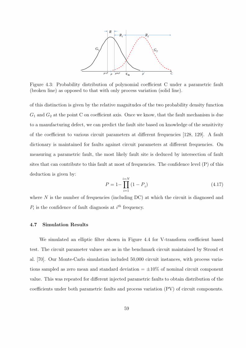
R1
m m’m+sm-s CCth
R2
R
G1 G2
Figure 4.3: Probability distribution of polynomial coefficient C under a parametric fault(broken line) as opposed to that with only process variation (solid line).
of this distinction is given by the relative magnitudes of the two probability density function
G1 and G2 at the point C on coefficient axis. Once we know, that the fault mechanism is due
to a manufacturing defect, we can predict the fault site based on knowledge of the sensitivity
of the coefficient to various circuit parameters at different frequencies [128, 129]. A fault
dictionary is maintained for faults against circuit parameters at different frequencies. On
measuring a parametric fault, the most likely fault site is deduced by intersection of fault
sites that can contribute to this fault at most of frequencies. The confidence level (P) of this
deduction is given by:
P = 1−i=N∏i=1
(1− P i) (4.17)
where N is the number of frequencies (including DC) at which the circuit is diagnosed and
Pi is the confidence of fault diagnosis at ith frequency.
4.7 Simulation Results
We simulated an elliptic filter shown in Figure 4.4 for V-transform coefficient based
test. The circuit parameter values are as in the benchmark circuit maintained by Stroud et
al. [70]. Our Monte-Carlo simulation included 50,000 circuit instances, with process varia-
tions sampled as zero mean and standard deviation = ±10% of nominal circuit component
value. This was repeated for different injected parametric faults to obtain distribution of the
coefficients under both parametric faults and process variation (PV) of circuit components.
59
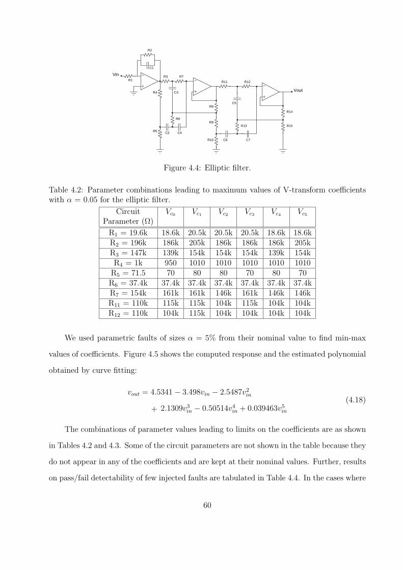
−
+−
+−
+Vout
VinR1
R2
R4
R5
R3 R7
R6
R8
R9
R10
R11 R12
R13
R14
R15
C1
C3
C4
C5
C6 C7
C2
Figure 4.4: Elliptic filter.
Table 4.2: Parameter combinations leading to maximum values of V-transform coefficientswith α = 0.05 for the elliptic filter.
Circuit Vc0 Vc1 Vc2 Vc3 Vc4 Vc5Parameter (Ω)
R1 = 19.6k 18.6k 20.5k 20.5k 20.5k 18.6k 18.6kR2 = 196k 186k 205k 186k 186k 186k 205kR3 = 147k 139k 154k 154k 154k 139k 154kR4 = 1k 950 1010 1010 1010 1010 1010R5 = 71.5 70 80 80 70 80 70R6 = 37.4k 37.4k 37.4k 37.4k 37.4k 37.4k 37.4kR7 = 154k 161k 161k 146k 161k 146k 146kR11 = 110k 115k 115k 104k 115k 104k 104kR12 = 110k 104k 115k 104k 104k 104k 104k
We used parametric faults of sizes α = 5% from their nominal value to find min-max
values of coefficients. Figure 4.5 shows the computed response and the estimated polynomial
obtained by curve fitting:
vout = 4.5341− 3.498vin − 2.5487v2in
+ 2.1309v3in − 0.50514v4in + 0.039463v5in
(4.18)
The combinations of parameter values leading to limits on the coefficients are as shown
in Tables 4.2 and 4.3. Some of the circuit parameters are not shown in the table because they
do not appear in any of the coefficients and are kept at their nominal values. Further, results
on pass/fail detectability of few injected faults are tabulated in Table 4.4. In the cases where
60
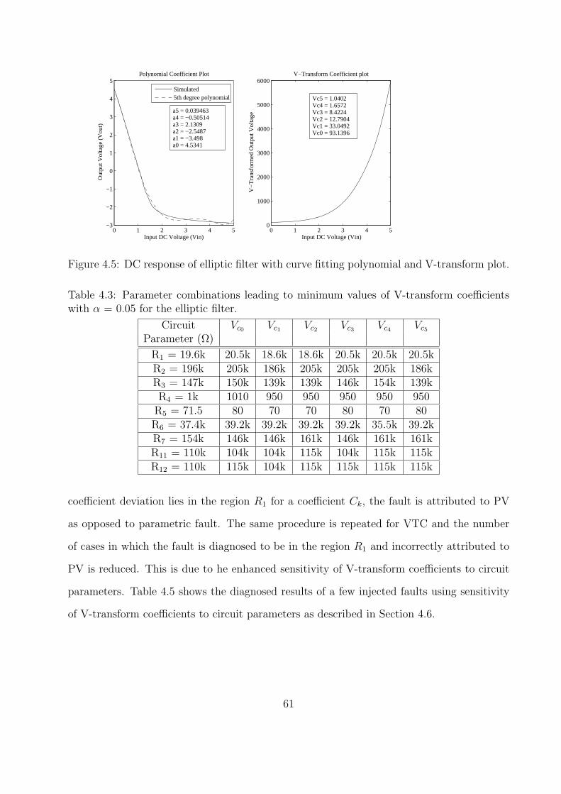
0 1 2 3 4 50
1000
2000
3000
4000
5000
6000V−Transform Coefficient plot
Input DC Voltage (Vin)
V−
Tra
nsfo
rmed
Out
put V
olta
ge
0 1 2 3 4 5−3
−2
−1
0
1
2
3
4
5
Out
put V
olta
ge (
Vou
t)
Polynomial Coefficient Plot
Input DC Voltage (Vin)
Simulated5th degree polynomial
a5 = 0.039463a4 = −0.50514a3 = 2.1309a2 = −2.5487a1 = −3.498a0 = 4.5341
Vc5 = 1.0402Vc4 = 1.6572Vc3 = 8.4224Vc2 = 12.7904Vc1 = 33.0492Vc0 = 93.1396
Figure 4.5: DC response of elliptic filter with curve fitting polynomial and V-transform plot.
Table 4.3: Parameter combinations leading to minimum values of V-transform coefficientswith α = 0.05 for the elliptic filter.
Circuit Vc0 Vc1 Vc2 Vc3 Vc4 Vc5Parameter (Ω)
R1 = 19.6k 20.5k 18.6k 18.6k 20.5k 20.5k 20.5kR2 = 196k 205k 186k 205k 205k 205k 186kR3 = 147k 150k 139k 139k 146k 154k 139kR4 = 1k 1010 950 950 950 950 950R5 = 71.5 80 70 70 80 70 80R6 = 37.4k 39.2k 39.2k 39.2k 39.2k 35.5k 39.2kR7 = 154k 146k 146k 161k 146k 161k 161kR11 = 110k 104k 104k 115k 104k 115k 115kR12 = 110k 115k 104k 115k 115k 115k 115k
coefficient deviation lies in the region R1 for a coefficient Ck, the fault is attributed to PV
as opposed to parametric fault. The same procedure is repeated for VTC and the number
of cases in which the fault is diagnosed to be in the region R1 and incorrectly attributed to
PV is reduced. This is due to he enhanced sensitivity of V-transform coefficients to circuit
parameters. Table 4.5 shows the diagnosed results of a few injected faults using sensitivity
of V-transform coefficients to circuit parameters as described in Section 4.6.
61
Table 4.4: Results for some injected faults in the elliptic filter.
Circuit Out of bound Fault Out of bound FaultParameter polynomial coefficient detected? V-transform coefficient detected?
R1 down 5% a3, a4 Yes Vc0 − Vc4 Yes
R2 down 10% a2 Yes Vc2 , Vc5 Yes
R3 up 5% a3 Yes Vc1 , Vc2 , Vc3 Yes
R4 down 10% a0 Yes Vc0 − Vc4 Yes
R5 up 10% a4 Yes Vc0 , Vc4 Yes
R7 up 5% None PV Vc1 , Vc2 Yes
R11 up 5% None PV Vc4 , Vc5 Yes
R12 down 5% None PV Vc4 , Vc5 Yes
Table 4.5: Parametric fault diagnosis with confidence levels of ≈ 88% for the elliptic filter.Injected Diagnosed fault sites Deducedfault DC 100Hz 900Hz 1000Hz 1100Hz fault
R1 R1 R1 R1, R2 R1, R2 R1 R1
dn 15% R4 C1 C1
R2 R2 R2 R2, R3 R2, R3 R2 R2
dn 10% C1 C1 C1
R3 R1 R3 R3, R4 R3 R3,C3 R3
up 5% R3 C3 C3 C3
R4 R1 R1 R2, R4 R1, R2 R1, R2 R4
dn 20% R4 R4 C1 R4 R4
R5 R5 R5 R4, R5 R4, R5 R5, R6 R5
up 15% C2 C2 C3
R7 R3 R7 R3, R7 R3, R6 R3, R7 R7
dn 10% R7 C3 R7 C3
4.8 Experimental Verification
Besides the simulation results presented in the previous section, we carried out an ex-
perimental validation of polynomial and V-transform coefficient based scheme for test and
diagnosis of parametric faults in the fifth-order elliptic filter that was analyzed in the previous
section. For all stimulus application and measurement, we used the National Instruments
Educational Laboratory Virtual Instrumentation Suite ELVIS-II+ [3] bench-top module. In
the sequel, we will briefly outline the details of the ELVIS II+ bench-top module and our
test setup. In Section 4.8.2, we present the measured results.
62

Figure 4.6: Test setup with elliptic filter built on the prototyping board, which is in turnmounted on the NI ELVISII+ bench-top module. Voltage and frequency control of theapplied signal is handled through the PC which is connected through USB port to thebench-top module. Output from the circuit is sampled and transferred through the sameUSB connection to the PC (where it can be post-processed). Also, circuit output can bedisplayed on the PC using a virtual oscilloscope utility available in the ELVIS software (seeFigure 4.7).
4.8.1 Test Setup
The NI ELVIS-II+ system consists of two modules. A hardware module comprises of
a bench-top module that houses a detachable prototyping board, several power supplies, a
function generator, multiple channel digital to analog and analog to digital converters and
terminals for oscilloscope and digital multimeter (DMM), all in one portable unit. The
second module, a computer interface referred to as ELVIS instrument launcher, provides a
software interface to control various utilities available on the hardware module.
The experimental set-up for our test scheme is shown in Figure 4.6. The test circuit
under test (CUT), a fifth-order elliptic filter, was realized using discrete, off-the-shelf com-
ponents such as three µA-741 type op-amps, seven electrolytic capacitors, and fifteen carbon
coated resistors. These components were mounted on the prototyping board that is housed in
63
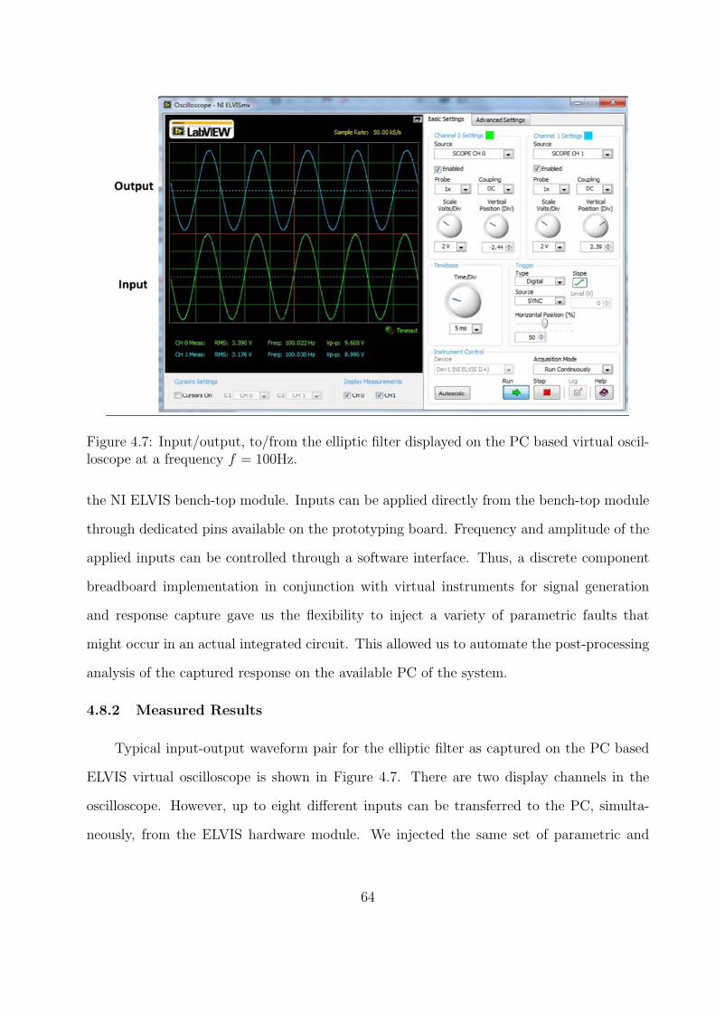
Figure 4.7: Input/output, to/from the elliptic filter displayed on the PC based virtual oscil-loscope at a frequency f = 100Hz.
the NI ELVIS bench-top module. Inputs can be applied directly from the bench-top module
through dedicated pins available on the prototyping board. Frequency and amplitude of the
applied inputs can be controlled through a software interface. Thus, a discrete component
breadboard implementation in conjunction with virtual instruments for signal generation
and response capture gave us the flexibility to inject a variety of parametric faults that
might occur in an actual integrated circuit. This allowed us to automate the post-processing
analysis of the captured response on the available PC of the system.
4.8.2 Measured Results
Typical input-output waveform pair for the elliptic filter as captured on the PC based
ELVIS virtual oscilloscope is shown in Figure 4.7. There are two display channels in the
oscilloscope. However, up to eight different inputs can be transferred to the PC, simulta-
neously, from the ELVIS hardware module. We injected the same set of parametric and
64
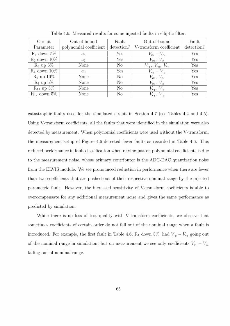
Table 4.6: Measured results for some injected faults in elliptic filter.
Circuit Out of bound Fault Out of bound FaultParameter polynomial coefficient detection? V-transform coefficient detection?
R1 down 5% a3 Yes Vc1 − Vc4 YesR2 down 10% a2 Yes Vc2 , Vc5 YesR3 up 5% None No Vc1 , Vc2 , Vc3 Yes
R4 down 10% a0 Yes Vc0 − Vc3 YesR5 up 10% None No Vc0 , Vc4 YesR7 up 5% None No Vc1 , Vc2 YesR11 up 5% None No Vc4 , Vc5 Yes
R12 down 5% None No Vc4 , Vc5 Yes
catastrophic faults used for the simulated circuit in Section 4.7 (see Tables 4.4 and 4.5).
Using V-transform coefficients, all the faults that were identified in the simulation were also
detected by measurement. When polynomial coefficients were used without the V-transform,
the measurement setup of Figure 4.6 detected fewer faults as recorded in Table 4.6. This
reduced performance in fault classification when relying just on polynomial coefficients is due
to the measurement noise, whose primary contributor is the ADC-DAC quantization noise
from the ELVIS module. We see pronounced reduction in performance when there are fewer
than two coefficients that are pushed out of their respective nominal range by the injected
parametric fault. However, the increased sensitivity of V-transform coefficients is able to
overcompensate for any additional measurement noise and gives the same performance as
predicted by simulation.
While there is no loss of test quality with V-transform coefficients, we observe that
sometimes coefficients of certain order do not fall out of the nominal range when a fault is
introduced. For example, the first fault in Table 4.6, R1 down 5%, had Vc0 − Vc4 going out
of the nominal range in simulation, but on measurement we see only coefficients Vc1 − Vc4
falling out of nominal range.
65

4.9 Sumamrizing V-Transform
In this chapter, a new approach for test and diagnosis of non-linear circuits based
on a transformation of polynomial expansion of the circuit was demonstrated. The V-
transform renders the polynomial coefficients monotonicity and enhances their sensitivity.
The minimum sizes of detectable faults in some of the circuit parameters are as low as 5%
which implies that impressive fault coverage can be achieved with V-transform coefficients.
The use of V-transform coefficients shows a reduction in masking of parametric faults due
to process variation. The method is then extended to sensitivity based fault diagnosis by
evaluating V-transform coefficients at different frequencies. The next chapter will examine
probability moments of the circuit output as a circuit-test signature, with circuit input as
noise (or random variable).
66

Chapter 5
Probability Moments as Test Signatures
5.1 Introduction
Defects in analog integrated circuits can be classified into two important categories,
namely, catastrophic faults (open or shorted components) and parametric faults (fractional
deviations of circuit components from their nominal values). While extensive literature [8,
15, 28, 41, 48, 76, 85, 143] exists on test schemes for detecting catastrophic (open/short)
faults, testing of parametric faults has not received similar attention [33, 45, 54, 157]. The
main reason for this disparity is that catastrophic faults tend to upset the supply current
drawn by the circuit or the output voltage by a reasonably large factor and any test scheme
based on their observation can conveniently uncover them. Some parametric faults have
little impact on supply current and are easily masked by measurement noise or general
insensitivity of the output to circuit parameter unless they are tested by careful designed
input signal targeting their excitation [111]. Different methods have been proposed to test
parametric faults in analog circuits including the use of neural networks [13, 34, 39, 130, 142],
spectral analysis [12, 158], transfer function coefficient based testing [53] or, more recently,
polynomial coefficient based testing [124, 125]. IDDQ measurement needs a sizable deviation
in a circuit component value from its nominal value to be useful [99]. Some test methods
require extra die area for testing or call for specific input signal excitation and increased
test time [77] (as is the case in neural networks based test methods). While some of these
problems are addressed in polynomial based test [124, 125], it is still in its early stages and
the correct choices of order and frequency of test points are critical for good fault coverage
Thus, we have a need for a production test, that has little additional hardware, reduced
test application time and minimized complexity of input signal design. To respond to the
67

last question we ask, ‘What is the easiest available signal that needs little or no design
effort?’ Without doubt, it is white noise, always available as random voltage fluctuations
across an R Ω resistor due to thermally agitated electrons. Power spectral density of this
white noise is given by SN (f) = 4kTR volt2/Hz, where k is the Boltzmann constant and T
is temperature in Kelvin. Previously [65] white noise has been used as an excitation signal
for testing circuits, and the output Fourier spectrum is used for ensuring the circuit conforms
to specification. However, in this work, to leverage a random signal like white noise which is
characterized only by its statistics such as mean, variance, third and higher order moments,
we compute probability moments at the output to be able to derive information on deviation
in circuit parameters. Reference [96] proposes the use of a pseudo random noise source as
the input and higher order statistics with Volterra kernel at the output as a signature for
characterizing the CUT as good or faulty. The work presented in this chapter differs on
three counts from previous work, 1) we use a truly random noise source as input, namely,
thermal noise from a resistor; though pseudo random noise source will work equally well,
2) higher order moments with an exponentially sensitive random variable transformation
is used at the output instead of Volterra kernel. Such a transformation gives better fault
resolution for parametric faults than Volterra kernel as shown by our simulation of the
elliptic filter example, those results are not included here, 3) we demonstrate fault diagnosis
in addition to testing while the earlier work discussed only testing. We view the circuit as a
communication channel [9, 115, 116] that transforms the probability density function of the
input signal as it propagates through the channel (circuit). The output, which is now the
transformed random variable (RV) has its signature moments that are used for testing the
CUT for both catastrophic and parametric faults. We show that probability moments can
be made exponentially sensitive [119, 127] to circuit parameters, so that parametric faults
of 10% and over result in sufficient excursions of the output probability moments to uncover
these faults. In the sequel, we describe our scheme on a cascaded amplifier and a low pass
filter. We then evaluate the performance of probability moments in conjunction with an
68
exponential RV transformation to enhance sensitivity for fault detection on a benchmark
elliptic filter.
Section 5.2 develops the background on moment theory and random variable transforma-
tion, and defines a minimum size detectable fault. The problem at hand and our approach is
described with examples in Section 5.3. In Section 5.4, we generalize the method to arbitrar-
ily large circuits. We report experimental results on benchmark elliptic filter in Section 5.5.
Section 5.6 introduces fault diagnosis procedure that leverages on unique relationships be-
tween moments and circuit components, and Section 5.7 reports results of a fault diagnosis
experiment using moments of output of a low noise amplifier. We conclude in Section 5.8.
5.2 Background
We briefly review the moment method to characterize a random variable (RV) (see [120]
for more details). We then give a transformation of RV to increase the sensitivity of moments
to circuit parameters.
5.2.1 Moment Generating Functions
The jth moment ∀j = 2 · · ·N of a continuous time RV X (t), sampled at time instants
t = kT , and denoted by Xk where k = 0, 1 · · ·∞ is given by
µj =∞∑k=0
(Xk − µ1)jp (Xk) (5.1)
Moment generating functionM (s) of such a discrete RVXk, serves as a convenient expression
from which different orders of moments µj may be computed using the following relation:
µj =djM (s)
dsj
∣∣∣∣s=0
(5.2)
where M (s) is given by
M (s) = E(esXk
)=
∞∑k=0
esXkp (Xk) (5.3)
69

5.2.2 Random Variable Transformation
We require a random variable transformation [94] that can narrowly track small changes.
We look for a transformation with following properties:
1. It increases the sensitivity of output function for small changes in the input.
2. It increases absolute values of the first and higher order moments of the output.
Let X be a RV whose domain is R. We define a transformation f (X) mapping X from
R =⇒ R as follows:
f (X) = XeαX− βX (5.4)
where α, β≥ 0 are parameters of the transformation. It can be shown that transformation
f (X) always gives second and higher order moments which are such that
loge |µj|f(X) ≥ loge |µj| ∀j = 2, 3, · · ·N (5.5)
We plot the first six moments of the transformed RV, with α = 0.01, β = 0.001 against
standard deviation of input RV in 5.1, which shows that the moments of the transformed
RV is always greater than that of the RV without transformation. At a few input standard
deviations, transformed RV can have significantly higher moments compared to moments
without transformation (Notice that the Y-axis in the plots are in the logarithmic scale).
This makes the transformation defined in equation 5.4 very amenable for use as a post
processing RV transformation at the output of the CUT. Even for small changes in the input,
the resulting moments can be significantly different. The sensitivity of the transformed RV
to the input RV is given by
SfX =
X
f
∂f
∂X= 1 + αX +
β
X(5.6)
By appropriate choice of α and β, based on dynamic range of X, we can increase the sensi-
tivity of f (X) for both small and large variations of X.
70

0 2 4 6 8 10−20
−10
0
10
20
Standard deviation of input RV
Mom
ent (
bel)
Order of moment = 1
0 2 4 6 8 10−50
0
50
100
150
200
Standard deviation of input RV
Mom
ent (
bel)
Order of moment = 2
0 2 4 6 8 10−50
0
50
100
150
Standard deviation of input RV
Mom
ent (
bel)
Order of moment = 3
0 2 4 6 8 10−50
0
50
100
150
Standard deviation of input RV
Mom
ent (
bel)
Order of moment = 4
0 2 4 6 8 10−50
0
50
100
150
200
Standard deviation of input RV
Mom
ent (
bel)
Order of moment = 5
0 2 4 6 8 10−50
0
50
100
150
200
250
Standard deviation of input RV
Mom
ent (
bel)
Order of moment = 6
Figure 5.1: Moments of different orders as functions of input noise power (standard deviationof input RV) with (in red/dashed) and without (in blue/solid) RV transformation for firstorder RC filter. See Figure 5.2.
71

R
C vovin
Figure 5.2: First-order RC filter.
5.2.3 Minimum Size Detectable Fault
Definition: Minimum size detectable fault (MSDF) of a circuit parameter is defined as
the minimum fractional deviation in the circuit parameter from its nominal value for it to
be detectable with all other circuit parameters held at their nominal values. The fractional
deviation ρ can be positive or negative and is named upside-MSDF (UMSDF) or downside-
MSDF (DMSDF) accordingly. This definition of minimum size detectable fault is general,
regardless of the test technique used to uncover faults. In the context of the test technique
described here, we define MSDF based on moments of the probability density function of the
circuit output. Suppose pi, where i = 1 · · ·K is the nominal value of ith circuit parameter
with a fault free tolerance range of pi (1± γ), and µj, where j = 1 · · ·N is the jth fault-free
probability moment of the circuit output. Then the UMSDF (DMSDF), ρi (ρi) of circuit
parameter pi is given by a minimum value x, such that pi (1± x) puts at least one of the
moments µj outside the fault free hypersphere |µj − µj| ≤ µ0, where µ0 is the permitted
deviation in moments when the circuit parameters are allowed excursions within their toler-
ance range. As specified earlier, this range is characterized by a tolerance factor γ.
5.3 Problem and Approach
We first illustrate with an example the calculation of limits of the probability moments
of a first order low pass filter. We follow this up with calculation of MSDF values of the
circuit parameters. We then consider a two stage cascade amplifier.
72

Vdd
R2R1 IM1 IM2
M1 M2
Vin
Vout
Figure 5.3: A cascade amplifier.
Example 1. First order RC filter: With white noise as the input, the discrete values are
sampled Gaussian RV of zero mean and variance, σ2in = No
2. The fault-free filtered response
has a variance (also the second order moment) µ2 =Noπ4RC
. Details of this calculation are shown
in the appendix. However, if there is a parametric fault of size x in the circuit parameter
R, then the new output variance is given by µ2 =Noπ
4R(1+x)C. If the circuit specifications can
tolerate a moment deviation of µ0, then the MSDF of R is given by the minimum value of x
that violates µ2 − µ2 ≤ µ0. For the example in question, since we consider only the second
order moment, the MSDF in R, denoted by ρR is given by
ρR =4µ0CR
Noπ − 4µ0CR(5.7)
Similarly MSDF of capacitor C, ρC can be found and by symmetry it is equal to ρR.
Example 2. Two stage amplifier: Consider the cascade amplifier shown in Figure 5.3.
The output voltage Vout in terms of input voltage results in a fourth degree polynomial:
vout = a0 + a1vin + a2v2in + a3v
3in + a4v
4in (5.8)
where constants a0, a1, a2, a3 are defined symbolically in (5.9) for transistors M1 and M2
operating in the saturation region.
73

a0 (R1, R2) = VDD −R2K(
WL
)2
(VDD − VT )2 +
R21K
2(
WL
)2
1V 4T−
2(VDD − VT )R1
(WL
)1V 2T
a1 (R1, R2) = R2K
(WL
)2
4R21K
2(
WL
)2
1V 3T
+2(VDD − VT )R1K(
WL
)1VT
a2 (R1, R2) = R2K
(WL
)2
2(VDD − VT )R1K(
WL
)1
−6R21K
2(
WL
)2
1V 2T
a3 (R1, R2) = 4VTK3
(WL
)2
1
(WL
)2
2R2
1R2
a4 (R1, R2) = −K3(
WL
)2
1
(WL
)2
2R2
1R2
(5.9)
If the cascade amplifier is excited with white noise at its input, the fault free output can be
a estimated as a random variable with its first order moment, namely, mean µ1 given by
µ1 = Ea0 + a1vin + a2v
2in + a3v
3in + a4v
4in
(5.10)
= a0 + a1µ1,in + a2µ2,in + a3µ3,in + a4µ4,in (5.11)
To find MSDF in R1, let us assume we have a fractional deviation x in R1 and the other
circuit parameters are at their fault free values. If µ0 is the tolerable fractional deviation in
the first order moment at the output, the minimum value of x that satisfies the following
inequality is the MSDF of parameter R1:
a0 (R1 (1 + x) , R2)
+a1 (R1 (1 + x) , R2)µ1,in
+a2 (R1 (1 + x) , R2)µ2,in
+a3 (R1 (1 + x) , R2)µ3,in
+a4 (R1 (1 + x) , R2)µ4,in
− µ1 ≥ µ0 (5.12)
Maximizing x, while meeting the constraint in equation 5.12 gives MSDF of R1 as
ρR1 =µ0
a0 + a1µ1,in + a2µ2,in + a3µ3,in + a4µ4,in
(5.13)
74

Table 5.1: MSDF for cascade amplifier of Figure 5.3 with µ0 = 0.05.
Circuit %upside %downsideparameter MSDF MSDF
Resistor R1 7 8Resistor R2 10.5 7.5
Similarly MSDF of R2 can be evaluated. Table 5.1 gives the MSDF for R1 and R2 based on
the above calculation. Nominal values of VDD = 1.2V , VT = 400mV ,(WL
)1= 1
2
(WL
)2= 20,
and K = 100µA/V 2 are used for this example.
5.4 Generalization
The computation of MSDF in the previous section is too complex for large circuits. As
shown in Figure 5.4 a complex circuit having more than 20 components is supplied the input
noise voltage (derived from a resistor maintained at desired temperature). The output of the
circuit is then passed through a suitable RV transformation function like the one given by
equation 5.4. Probability density function (PDF) of the output of this RV transformation is
estimated using the histogram spread of the output voltage values. Next, N th order moments
(orders up to N = 6 are sufficient for most analog circuits having component count of ≤ 40)
are found using the moment generating function defined in equation 5.3. The jth derivatives
w.r.t. s required for jth order moments are found as finite differences about s = 0. Once the
fault free values of all N moments are available, single parametric faults are injected into the
circuit and the corresponding deviation in one or more moments are noted. Based on the
moment deviations that can be tolerated, the fault size injected is steadily increased. The
minimum fault size of any circuit parameter that causes at least one of the moments to just
fall outside of its tolerance band (also called the fault-free hypersphere) gives the MSDF of
that circuit parameter. In Figure 5.5, Flowchart I summarizes the process of numerically
finding the probability moments and their bounds and Flowchart II in Figure 5.5 outlines
a procedure to test CUT using the PDF moments. The bounds on moments of fault free
circuit are found a priori in Flowchart I.
75

Vn2 = 4kTR
+
-
CUT
ADC
DSP
Pass/Fail
ATE
Compute
&
Compare
ROM
Golden
Moments
Figure 5.4: Block diagram of a system with CUT using white noise excitation.
5.5 Fault Detection in Elliptic Filter
We simulated an elliptic filter shown in Figure 5.6 according to the test scheme of
Figure 5.5. The circuit parameter values are as in the benchmark maintained by Stroud et
al. [70]. Thermal noise from resistors R = 40GΩ, 60GΩ, 80GΩ, 100GΩ was used at T =
300K. On application of RV transformation, signal levels (and so are moments) significantly
better resolved as compared to that without RV transformation. For example, the six fault
free moments of the elliptic filter before transformation (for R = 40GΩ) are as follows:
µ1 = 4.53453, µ2 = 0.03234, µ3 = 0.02345, µ4 = 0.01125, µ5 = 0.009325, µ6 = 0.00623125.
After RV transformation, the fault free moments are given by µ1 = 338.6453, µ2 = 1.8234,
µ3 = 0.9254, µ4 = 0.8812, µ5 = 0.6365, µ6 = 0.1638125.
Combinations of parameter values leading to limits on the coefficients are as shown in
Tables 5.2 and 5.3. Results on pass/fail detectability of few injected faults are tabulated in
Table 5.4.
76

Start
Stop
Simulate for all single parametric
faults to find respective MSDF
Apply noise excitation
and note corresponding
output voltage levels
Apply desired RV transformation
on circuit output
Estimate PDF and compute
moments using Moment
generating function
Start
Estimate
moments µµµµi∀ i=1…N
Apply desired
RV transformation
on circuit output
Apply noise excitation
and note corresponding
output voltage levels
| µµµµi| > | µµµµi(1+ µ0)| or | µµµµi | < | µµµµi(1- µ0)|
i = 1
i = i+1
i < N ?
Subject CUT
to further tests
CUT is faulty
No
Yes
No
Yes
Stop
Flowchart I Flowchart II
Figure 5.5: Fault simulation process and bounding of moments (Flowchart I), and the com-plete test procedure (Flowchart II).
77
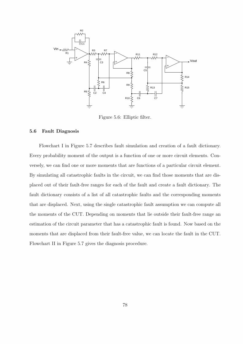
−
+−
+−
+Vout
VinR1
R2
R4
R5
R3 R7
R6
R8
R9
R10
R11 R12
R13
R14
R15
C1
C3
C4
C5
C6 C7
C2
Figure 5.6: Elliptic filter.
5.6 Fault Diagnosis
Flowchart I in Figure 5.7 describes fault simulation and creation of a fault dictionary.
Every probability moment of the output is a function of one or more circuit elements. Con-
versely, we can find one or more moments that are functions of a particular circuit element.
By simulating all catastrophic faults in the circuit, we can find those moments that are dis-
placed out of their fault-free ranges for each of the fault and create a fault dictionary. The
fault dictionary consists of a list of all catastrophic faults and the corresponding moments
that are displaced. Next, using the single catastrophic fault assumption we can compute all
the moments of the CUT. Depending on moments that lie outside their fault-free range an
estimation of the circuit parameter that has a catastrophic fault is found. Now based on the
moments that are displaced from their fault-free value, we can locate the fault in the CUT.
Flowchart II in Figure 5.7 gives the diagnosis procedure.
78

Start
Apply Noise excitation at the Inputand note corresponding
output voltage levels
Compute moments ofof the circuit outputto the desired order
Start
Apply Noise excitation at the Inputof CUT and note corresponding
output voltage levels
Compute moments ofof the CUT
Retain moments that lie outside of their tolerance band
Inject Catastrophic fault in the circuit netlist
Stop
Create fault dictionary noting moments that deviate beyond
tolerance for every fault simulated
Stop
Look up the fault dictionary for deducing possible fault sites that cause
similar deviations in moments
All faults simulated?
Record moments that deviate beyond
tolerance
YES
NO
Flowchart II
Flowchart I
Figure 5.7: Fault simulation (Flowchart I) and Fault diagnosis (Flowchart II) proceduressummarized.
79

Table 5.2: Parameter combinations leading to maximum values of moments with devicetolerance γ = 0.05 in elliptic filter.
Circuit µ1 µ2 µ3 µ4 µ5 µ6
Parameter (Ω, nF)
R1 = 19.6k 19.6k 20.58k 19.6k 20.58k 20.58k 18.62k
R2 = 196k 186.2k 205.8k 205.8k 205.8k 186.2k 186.2k
R3 = 147k 139.65k 147k 139.65k 139.65k 154.35k 147k
R4 = 1k 1050 1050 950 1000 1050 950
R5 = 71.5 75.075 67.925 75.075 71.5 75.075 67.925
R6 = 37.4k 37.4k 37.4k 37.4k 39.27k 39.27k 37.4k
R7 = 154k 154k 154k 154k 146.3k 154k 154k
R8 = 260 260 260 260 260 273 273
R9 = 740 703 777 777 703 777 777
R10 = 500 500 500 475 475 525 500
R11 = 110k 115.5k 104.5k 104.5k 104.5k 104.5k 110k
R12 = 110k 115.5k 104.5k 104.5k 110k 110k 115.5k
R13 = 27.4k 28.77k 26.03k 26.03k 26.03k 27.4k 26.03k
R14 = 40 40 40 38 40 40 40
R15 = 960 912 1008 912 960 912 960
C1 = 2.67 2.8035 2.5365 2.67 2.67 2.67 2.5365
C2 = 2.67 2.8035 2.67 2.8035 2.8035 2.5365 2.67
C3 = 2.67 2.8035 2.8035 2.67 2.5365 2.5365 2.5365
C4 = 2.67 2.8035 2.67 2.5365 2.67 2.5365 2.67
C5 = 2.67 2.8035 2.67 2.8035 2.5365 2.5365 2.67
C6 = 2.67 2.8035 2.5365 2.8035 2.5365 2.67 2.8035
C7 = 2.67 2.67 2.5365 2.8035 2.8035 2.67 2.5365
5.7 Fault Diagnosis in Low Noise Amplifier
We used the low noise amplifier of Figure 5.8 to evaluate our test procedure. The circuit
has 16 components. Thus, there are 32 single catastrophic faults corresponding to opens and
shorts of the passive R, L and C elements. For an open fault, the element was replaced
by a 1GΩ resistance. For a short fault, the element was replaced by a 0V voltage source.
For the MOS transistor, the drain and source terminals were short circuited for a short and
were left open for an open fault. For these 32 faults to be uniquely identified, we need at
least 5 moments. Each fault causes one or more moments to lie outside its tolerance band.
The total number of uniquely identifiable fault cases with N moments = ΣNn=1
(Nn
)= 2N − 1.
Two faults displacing the same set of moments will cause a diagnostic ambiguity. Evaluating
80
higher order moments, however, gives better diagnostic resolution, which comes at a price of
additional computation. Table 5.5 lists faults and the corresponding moments displaced by
each fault. We use up to the 6th order moment and observe that out of the 32 faults, only 5
are not uniquely diagnosed because they affect identical sets of moments. The number in the
last column identifies number of faults displacing the same set of moments. For example, two
faults (indicated in the last column) Rbias-short and Lc-short displace same set of moments
µ2–µ6.
5.8 Conclusion
This chapter discussed a new approach for test and diagnosis of non-linear circuits based
on probability density moments of the output was presented. We also showed the effective use
of RV transformation to sensitize the output moments to circuit parameters. The minimum
sizes of detectable faults in some of the circuit parameters are as low as 10% for an elliptic
filter, which implies impressive fault coverage can be achieved with moments as a test metric.
Further, the prudent choice of RV transformations can enhance the fault detection resolution.
We also proposed a method for localizing catastrophic faults and showed that good diagnostic
coverages can be obtained by choosing expansions of moments of the order O(ln(N)) for N
faults.
The next chapter examines the upper bound on defect level and lower bound on fault
coverage achievable in signature based test techniques proposed in this chapter and the
previous two chapters – namely polynomial coefficients and V-transform coefficients. The
approach taken is general enough that bounds derived can be easily extended to any other
coefficient-based signature-test schemes.
81
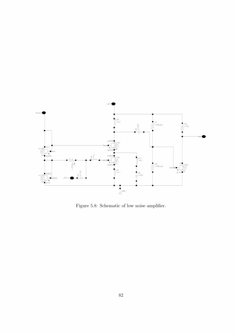
Figure 5.8: Schematic of low noise amplifier.
82

Table 5.3: Parameter combinations leading to minimum values of moments with devicetolerance γ = 0.05 in elliptic filter.
Circuit µ1 µ2 µ3 µ4 µ5 µ6
Parameter (Ω,nF)
R1 = 19.6k 19.6k 18.62k 19.6k 19.6k 19.6k 20.58k
R2 = 196k 205.8k 205.8k 205.8k 196k 186.2k 205.8k
R3 = 147k 147k 154.35k 154.35k 139.65k 154.35k 154.35k
R4 = 1k 950 1000 1050 950 1050 950
R5 = 71.5 67.925 71.5 75.075 75.075 67.925 71.5
R6 = 37.4k 39.27k 37.4k 35.53k 39.27k 35.53k 35.53k
R7 = 154k 146.3k 161.7k 154k 161.7k 154k 154k
R8 = 260 247 273 247 273 260 247
R9 = 740 703 777 740 777 777 740
R10 = 500 500 500 475 475 525 475
R11 = 110k 104.5k 115.5k 115.5k 115.5k 110k 110k
R12 = 110k 115.5k 110k 115.5k 110k 104.5k 115.5k
R13 = 27.4k 27.4k 26.03k 27.4k 28.77k 28.77k 26.03k
R14 = 40 42 40 40 38 40 38
R15 = 960 1008 960 1008 1008 912 960
C1 = 2.67 2.67 2.5365 2.5365 2.67 2.5365 2.67
C2 = 2.67 2.67 2.67 2.67 2.67 2.67 2.8035
C3 = 2.67 2.8035 2.8035 2.8035 2.8035 2.5365 2.8035
C4 = 2.67 2.8035 2.8035 2.8035 2.8035 2.8035 2.67
C5 = 2.67 2.67 2.8035 2.67 2.8035 2.8035 2.67
C6 = 2.67 2.8035 2.5365 2.8035 2.5365 2.67 2.8035
C7 = 2.67 2.67 2.5365 2.8035 2.67 2.67 2.8035
Table 5.4: Fault detection of some injected faults in elliptic filter.
Circuit Parameter Out of bound moment Fault detected?
R1 down 12% µ3, µ1 Yes
R2 down 10% µ4 Yes
R3 up 12% µ1, µ2 Yes
R4 down 10% µ2 Yes
R5 up 10% µ4 Yes
R7 up 15% µ5, µ6 Yes
R11 up 15% µ3 Yes
R12 down 15% µ2, µ6 Yes
C1 up 11% µ1, µ2 Yes
C4 up 12% µ4 Yes
C5 down 15% µ1, µ6 Yes
83

Table 5.5: Fault dictionary for catastrophic faults in low noise amplifier.
Component Nature µ1 µ2 µ3 µ4 µ5 µ6 Uniquely(ohm, nH, fF) of fault Diagnosable?
Rbias = 10 short X X X X X No (2)
LC = 1 short X X X X X No (2)
L1 = 1.5 short X X X X X X Yes
L2 = 1.5 short X X X X Yes
Lf = 1 short X X X X X X No (3)
Cf = 100 short X X X Yes
CC2 = 100 short X X X X X Yes
Rbias1 = 100k short X X X Yes
Rbias2 = 100k short X X Yes
RL = 100k short X X X No (3)
N0(D− S) short X X Yes
N1(D− S) short X X Yes
N2(D− S) short X X X X X Yes
N3(D− S) short X X X X X Yes
N4(D− S) short X X Yes
Rbias = 10 open X X X Yes
LC = 1 open X X Yes
L1 = 1.5 open X X X Yes
L2 = 1.5 open X X X X Yes
Lf = 1 open X X X Yes
Cf = 100 open X X X Yes
CC2 = 100 open X Yes
Rbias1 = 100k open X X X Yes
Rbias2 = 100k open X X X X Yes
RL = 100k open X X X X X X No (3)
N0(D− S) open X X X Yes
N1(D− S) open X X X X Yes
N2(D− S) open X Yes
N3(D− S) open X X X Yes
N4(D− S) open X X Yes
84

Chapter 6
Bounds on Fault Coverage and Defect Level in Signature Based Testing
6.1 Introduction
Faults in analog circuits can be fundamentally divided into two categories, namely,
catastrophic and parametric [33]. Catastrophic faults are those in which a circuit component
displays extreme deviant behavior from its nominal value. For example, in a resistor such
a fault could either be an electrical open or short. Such faults are easy to uncover because
they manifest themselves as a sizable deviation in circuit output or performance. On the
other hand, component faults are fractional deviations in circuit components from their
nominal values. They manifest themselves as subtle deviations in output or performance of
the circuit. It is therefore a non-trivial problem to uncover component faults.
Component-based testing of analog circuits has been widely discussed in the litera-
ture [16, 37, 53, 92, 93, 100, 111]. Typical methods of characterizing input-output relation-
ship is based on coefficients of transfer function [53], polynomial expansion [124], wavelet
transform [23], V-transform [119] or Volterra series [96].
A popular and elegant method was proposed by Savir and Guo [53], in which, analog
circuit under test is treated as a linear time invariant (LTI) system. The transfer function
(TF) of this LTI system is computed based on the circuit netlist. Note that the coefficients in
the numerator and denominator of TF, referred to as transfer function coefficients (TFC), are
functions of circuit components. Therefore, any drift in circuit components from their fault
free (nominal) values will also result in drifts of the coefficients, as they are linear functions
of circuit components. As a result min-max bounds for the coefficients of a healthy circuit
are found and these are used to classify the circuit under test (CUT) as good or faulty.
Reference [111] shows some limitations of component based analog testing by treating CUT
85

this way. However, there has been no effort to quantify the achievable fault coverage (FC)
and defect level (DL) in TFC based testing of analog circuits. In this work we have derived
closed form expressions for upper bound on DL and lower bound on FC.
An approach proposed by Savir and Guo [53] finds component faults by measuring the
TFC estimates of the CUT. Minimum size detectable fault (MSDF) in their method is de-
fined as the minimum fault size or minimum fractional drift of the circuit component that will
cause the circuit characteristic (in this case the TFC) to lie beyond its permissible limits [53].
In general, computation of MSDF for a circuit component is a non-linear optimization prob-
lem and it is computationally expensive to evaluate MSDF for all the circuit components.
However, we have some respite in TFCs of linear analog circuit being a linear functions of
the circuit components. This implies that TFCs of the circuit take min-max values when
at least one of the circuit component is at the edge of its tolerance band (fault free drift
range) [53]. This fact is used to avoid solving the non-linear optimization problem. Instead,
the circuit is simulated for all combinations of extreme values taken by circuit components
in its fault free drift range. The minimum deviation in circuit components causing the coef-
ficients to move out of their min-max bands is thus obtained and is called nearly minimum
size detectable fault (NMSDF). The price paid for this simplification is the non-zero differ-
ence between NMSDF and MSDF. We quantify this difference and thereby derive bounds
for the defect level and Fault coverage achievable through TFC based test methods. Main
results of this work have appeared recently [123]. In addition, we present a trade-off between
computational overheads of simulation vis-a-vis the effort required to solve the non-linear
optimization problem based on the defect level desired.
Most of the ideas in this chapter have been published in a paper [121]. This chapter is
organized as follows. In Section 6.2 we formulate the problem. Section 6.3 describes our ap-
proach and present analytical proofs for the bounds on DL and FC. Section 6.4 comprises the
86
simulation results for some well-known circuits. Section 6.5 is a discussion on “simulation–
optimization” trade-off based on bounds of defect level and fault coverage. Section 6.6
concludes the chapter.
6.2 Problem Formulation
A linear analog circuit [38, 61, 68] can be represented as a LTI system whose transfer
function is given by,
H(s) = K
sλ +λ−1∑k=0
aksk
sµ +µ−1∑k=0
bksk(λ < µ) (6.1)
Consider a linear analog circuit made up of N circuit components. In the literature, com-
ponents are often referred to as circuit parameters. However, we will consistently refer
to the circuit elements as components. We assume that components have nominal values,
pni, ∀i = 1 . . . N . In (1), coefficients K, ak and bk are functions of the circuit com-
ponents. Let the specified fractional tolerance range for each component be ±α centered
around its nominal value. Thus, the range of values for component pi is,
pni(1− α) ≤ pi ≤ pni(1 + α) ∀i = 1 · · ·N (6.2)
The set of all fault free or undetectable fault values taken by any coefficient ai in (1)
is contained in [ai,min, ai,max]. Let Ck be one of the coefficients of the LTI system transfer
function in (1). Clearly, Ck is a function of at least one or more circuit components pi ∀i =
1 . . . N . Each coefficient Ck ∀k = 0, . . . , (λ+µ+1) is enclosed in an N -dimensional hypercube
spanned by the circuit components. The volume of this hypercube depends on the fault
free tolerance range of the circuit components that determine Ck. The extremities of any
coefficient Ck of the transfer function occur when at least one component is outside its
tolerance range. The circuit is simulated only at the edges of the hypercube. The maximum
and minimum values of a coefficient Ck are thus obtained form its bounds.
87

Figure 6.1: Hypercube around coefficient Ck and associated regions.
We formally define the following terms as they are used here.
Definition 1 : Minimum size detectable fault (MSDF) of a component pi is the smallest
fractional change ρi in its value that makes the circuit faulty when all the other components
retain their nominal values.
Definition 2 : Nearly minimum size detectable fault (NMSDF) of a component pi is any
small fractional change ρ∗i in its value that makes the circuit faulty when all other compo-
nents retain their nominal values. Note that ρ∗i ≥ ρi, ∀i = 1 . . . N .
Definition 3 : Coefficient of uncertainty (ϵi) is the assumed difference between the
NMSDF and MSDF for the ith circuit component. That is,
ϵi= ρ∗i−ρi (6.3)
88
Definition 4 : Defect level (DL) of a test procedure is the probability of a faulty circuit
passing the test as a fault free circuit.
Definition 5 : Fault coverage (FC) of a test procedure is the fraction of all detectable
faults that can be detected in CUT by the test procedure.
Consider a TFC Ck being a function of components p1 and p2. The hypercube enclosing
Ck is shown in Figure 6.1. MSDF values of p1 and p2 are found by solving a non-linear
optimization problem [53]. The objective for the solution is to maximize (or minimize) Ck
with constraint on p1 and p2, allowing a drift of ±α about its nominal value. An example
of MSDF calculation has been illustrated by Savir and Guo [53]. NMSDF for p1 and p2
are obtained by simulating the circuit at the vertices of the hypercube and measuring the
fractional changes in the value of Ck. In general, the MSDF (ρ) and NMSDF (ρ∗) values of
a component for drifts above and below its nominal values are not the same. However, for
the sake of developing a conservative bound and ease of calculation we consider ρ = Min
(ρ↑, ρ↓) and ρ∗= Max (ρ∗↑, ρ
∗↓). Where ρ↑ and ρ↓ denote positive and negative MSDF and ρ∗↑
and ρ∗↓ denote positive and negative NMSDF.
Shaded region Λ in Figure 6.1 is the region of uncertainty and any component drift
leading to coefficient lying in this region goes undetected. This region contributes to the
defect level DLCkwhen the test is based on observing the coefficient Ck.
6.3 Our Approach
6.3.1 Bounding Defect level
The values taken by circuit components can be modeled as independent and identically
distributed random variables whose means are the nominal fault-free values and standard
deviations (σ) are the tolerance values of circuit components [70].
Two component case
We assume a normal distribution of the components p1 and p2 with mean values same
as their nominal values (p1n and p2n) and variance σ2. The defect level from measurement
89
of coefficient Ck alone is obtained by integrating the joint probability density function of
components p1 and p2 over the shaded area Λk shown in Figure 6.1 and is given by,
DLCk=
∫Λk
fp1,p2(x, y) dx dy (6.4)
where fp1,p2(x, y) is the joint probability density function (p.d.f.) of p1 and p2 as given by,
fp1,p2(x, y) =1
2πσ2exp
(−(x− p1n)
2
2σ2+
−(y − p2n)2
2σ2
)(6.5)
We define Q(x) as the integral over the interval [x, ∞) of a zero mean and unity variance
normal distribution [94]. Similarly, two more integrals, S1 and S2, are defined as follows:
Q(x) =1√2π
∞∫x
exp
(−u2
2
)du (6.6)
S1 =
p1n(1+α)∫p1n(1−α)
p2n(1+α)∫p2n(1−α)
fp1,p2(x, y) dx dy (6.7)
S2 =
p1n(1+α)∫p1n(1−α)
p2n(1+α−ϵ)∫p2n(1−α+ϵ)
fp1,p2 (x, y) dx dy (6.8)
S1 and S2 are evaluated by integrating over the areas shown in Figure 6.1. The Defect Level
obtained on observing only a single coefficient Ck is given by,
S1 =
Q
(−ασ
)−Q
(ασ
)2
S2 =
Q
(−ασ
)−Q
(ασ
)Q
(−α+ ε
σ
)−Q
(α− ε
σ
)
DLCk= S1 − S2 (6.9)
90
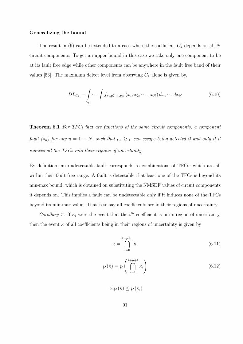
Generalizing the bound
The result in (9) can be extended to a case where the coefficient Ck depends on all N
circuit components. To get an upper bound in this case we take only one component to be
at its fault free edge while other components can be anywhere in the fault free band of their
values [53]. The maximum defect level from observing Ck alone is given by,
DLCk=
∫Λk
· · ·∫fp1,p2,··· ,pN (x1, x2, · · · , xN) dx1 · · · dxN (6.10)
Theorem 6.1 For TFCs that are functions of the same circuit components, a component
fault (ρn) for any n = 1 . . . N , such that ρn ≥ ρ can escape being detected if and only if it
induces all the TFCs into their regions of uncertainty.
By definition, an undetectable fault corresponds to combinations of TFCs, which are all
within their fault free range. A fault is detectable if at least one of the TFCs is beyond its
min-max bound, which is obtained on substituting the NMSDF values of circuit components
it depends on. This implies a fault can be undetectable only if it induces none of the TFCs
beyond its min-max value. That is to say all coefficients are in their regions of uncertainty.
Corollary 1 : If κi were the event that the ith coefficient is in its region of uncertainty,
then the event κ of all coefficients being in their regions of uncertainty is given by
κ =
λ+µ+1∩i=0
κi (6.11)
℘ (κ) = ℘
(λ+µ+1∩i=1
κi
)(6.12)
⇒ ℘ (κ) ≤ ℘ (κi)
91

where ℘ (κ) denotes probability of event κ. Equation (12) follows from the fact that κi ⊇ κ.
From (12) and the definition of defect level (DL) as stated in Definition 4, we get
DLCk≥ DL (6.13)
From (10), upper bounds on DLCkand DL are obtained for N circuit components, assuming
that each component has an identical coefficient of uncertainty ϵ. We get the following result:
DL ≤ DLCk≤Q(−α
σ
)−Q
(ασ
)N−Q(−α
σ
)−Q
(ασ
) Q(−α+ϵ
σ
)−Q
(α−ϵσ
)N−1(6.14)
An analog circuit is typically designed anticipating ±σ variation in its component values [70],
where σ is the standard deviation or tolerance of a component about its nominal value and
is usually known a priori as a specification of the device. We can therefore assume fault free
drifts of ±α about the nominal value of the circuit component to be equal to ±σ variation
in the value of component. Substituting ±α = ±σ in (14), we get a conservative bound on
defect level as,
DL ≤ 0.8427N − 0.8427
Q(−1 +
ϵ
σ
)−Q
(1 +
−ϵσ
)N−1
(6.15)
6.3.2 Bounding Fault Coverage
Just as we dealt with the problem of bounding the defect level, we shall first consider
the two component case and then generalize the result for N components.
Two component case
We assume a normal distribution for each of the components p1 and p2 with mean as
the nominal value, p1n or p2n, and variance σ2. We also regard their probability distributions
being independent of each other. The Fault coverage achievable by observing coefficient Ck
alone is obtained by integrating the joint probability density function of p1 and p2 over the
92

shaded area Γk in Figure 6.1. Thus,
FCCk=
∫Γk
fp1,p2(x, y) dx dy (6.16)
where region Γk is the complement of union of region of uncertainty Λk and fault free space
Ξk of coefficient Ck in quadrant-I in which p1, p2 ∈ (0,∞). This is the entire region in the
quadrant-I denoted as Ω. We can write,
Γk= Ω\ (Λk ∪ Ξk) (6.17)
SΩ =
Q
(−p1nσ
)Q
(−p2nσ
)(6.18)
SΩ in (18) gives probability of the region under Ω. From (17) and (18), we have FCCk
given by (19).
FCCk=Q(−p1n
σ
)Q(−p2n
σ
)−Q(−α
σ
)−Q
(ασ
)2 (6.19)
In general, nominal value of a component is much greater than its tolerance [70]. We
can therefore fairly assume pin = 5σ ∀ i = 1 . . . N and ±α = ±3σ in (19) to find FCCkfor
two components.
Generalizing the bound
Equation (16) can be extended to N components as in (20).
FCCk=
∫Γk
· · ·∫fp1,p2,··· ,pN (x1, x2, · · · , xN) dx1 · · · dxN (6.20)
Theorem 6.2 For TFCs that are functions of the same circuit components, a component
fault (ρn) for any n=1 . . .N such that ρn ≥ ρ∗ can be detected if and only if it induces at
least one of the TFCs beyond their regions of uncertainty.
93

By converse of the statement of Theorem 6.1 we have Theorem 6.2.
Corollary 2: If ηi were the event that the ith coefficient is in its region of detectability
(Γi), then the event η of at least one of the coefficients being in their region of detectability
is given by
η =
λ+µ+1∪i=0
ηi (6.21)
Equation (22) follows from (21) as we have ηi ⊆ η.
℘ (η) ≥ ℘ (ηi) (6.22)
By definition 5 we have FCCk= ℘ (ηi) and FC = ℘ (η) therefore on evaluating the
integral in (20) we get
FC ≥ FCCk=
N∏i=1
Q
(−pinσ
)−Q
(−ασ
)−Q
(ασ
)N
(6.23)
The result in (23) is a lower bound on fault coverage. On substituting typical values
for nominal component, (pin = 5σ and ±α = ±σ), we get the following result, which is
independent of ϵ:
FC ≥ FCCk= 1− 0.8427N (6.24)
6.4 Simulation and Computation
We present plots of defect level in (6.15) against the number of circuit components (N)
in Figure 6.2 and against the ratio of coefficient of uncertainty (ϵ) to standard deviation (σ)
in Figure 6.3. Figure 6.5 shows the plots of simulated and computed values (from (6.15)) of
defect level for different N and ϵ = 0.1 for an RC ladder filter which we will now discuss.
To gain insight, we examined RC ladder filter networks of varying number (n) of RC
sections as shown in Figure 6.4. The number of components is 2n. The transfer function
94
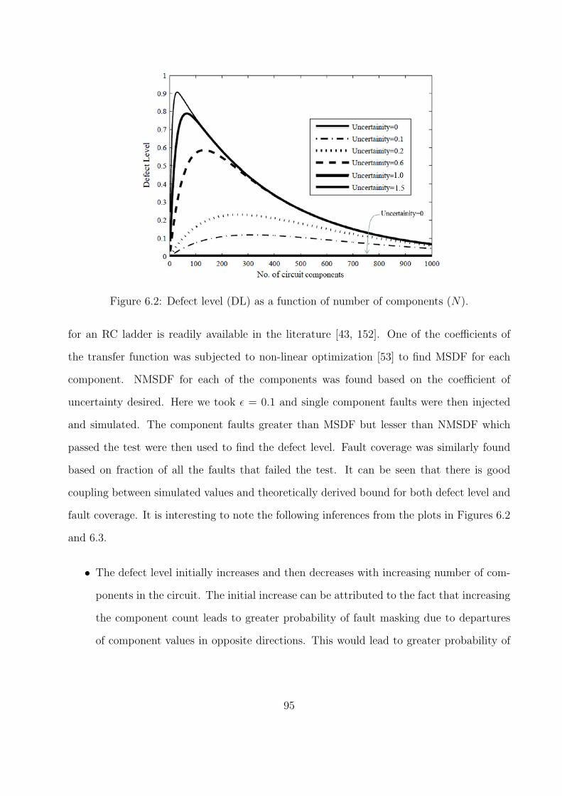
Figure 6.2: Defect level (DL) as a function of number of components (N).
for an RC ladder is readily available in the literature [43, 152]. One of the coefficients of
the transfer function was subjected to non-linear optimization [53] to find MSDF for each
component. NMSDF for each of the components was found based on the coefficient of
uncertainty desired. Here we took ϵ = 0.1 and single component faults were then injected
and simulated. The component faults greater than MSDF but lesser than NMSDF which
passed the test were then used to find the defect level. Fault coverage was similarly found
based on fraction of all the faults that failed the test. It can be seen that there is good
coupling between simulated values and theoretically derived bound for both defect level and
fault coverage. It is interesting to note the following inferences from the plots in Figures 6.2
and 6.3.
• The defect level initially increases and then decreases with increasing number of com-
ponents in the circuit. The initial increase can be attributed to the fact that increasing
the component count leads to greater probability of fault masking due to departures
of component values in opposite directions. This would lead to greater probability of
95

Figure 6.3: Defect level (DL) plotted against ratio of coefficient of uncertainty to toleranceof components ( ϵ
σ).
fault being masked. However, contrary to intuition, component values beyond a cer-
tain threshold result in decrease of defect level. This is a manifestation of stochastic
resonance, in that, a circuit with large number of components can aid those sections
of circuit that induce faults in opposite directions, thereby resulting in a lower defect
level.
• In Figure 6.2, we can see that for medium number of components, defect level is
relatively unchanged for larger coefficients of uncertainty. On the contrary ϵ has to be
made far smaller to gain in defect level.
• Fault coverage monotonically increases with the number of components as in Figure 6.3.
An increase in number of components implies a greater observability for each coefficient.
Increased observability is due to the fact that every added component need not increase
the count of number of coefficients. For example, a resistor added may not increase the
order of the circuit. This leads to more circuit components per coefficient and hence
96

Figure 6.4: RC ladder filter network of n stages.
an increased observability. This in turn increases fault coverage as more components
now have a bearing on circuit TFCs.
To further validate the bounds derived, we simulated and tested TFC based approach
on benchmark circuits proposed and maintained by Kondagunturi et al. [70]. These are
SPICE models from ITC’97 benchmark circuits and Statistical Fault Analyzer (SFA) based
models proposed by Epstein et al. [42]. The fault model chosen by us for component faults
(soft faults) is σ deviation from nominal value and for catastrophic faults we used open/short
faults. To obtain the fault coverage values, we used simulation. Each sample circuit contained
a single component fault of size ±σ,±2σ, · · · ,±10σ (without allowing negative component
values), and was simulated to determine whether the fault was uncovered by the TFC based
approach for the chosen value of coefficient of uncertainty. We chose ϵσ= 0.1. The computed
and simulated values of defect level and fault coverage for each of the benchmark circuits are
tabulated in Table 6.1. In the table, the benchmark with largest component count, ITC’97e,
has about 35 components. As a result, we could not verify the tightness of bounds on large
component count circuits. To circumvent this predicament, we relied on the RC ladder filter
network of Section 6.4. Computed bound and simulated values of defect level as a function
of component count are shown in Figure 6.5.
6.5 Simulation Versus Optimization: A Trade-off
We now introduce the “simulation-optimization” tradeoff that results in a typical TFC
based analog circuit test scenario. For circuits with more than ten components, the time
97
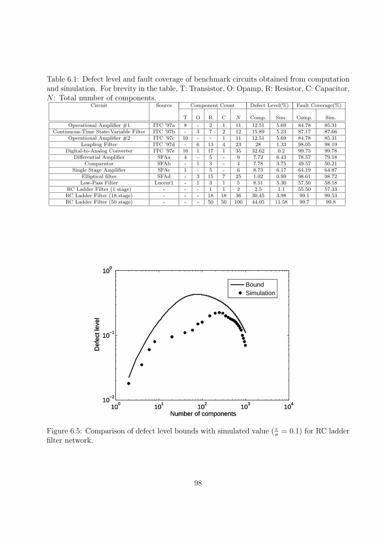
Table 6.1: Defect level and fault coverage of benchmark circuits obtained from computationand simulation. For brevity in the table, T: Transistor, O: Opamp, R: Resistor, C: Capacitor,N : Total number of components.
Circuit Source Component Count Defect Level(%) Fault Coverage(%)
T O R C N Comp. Sim. Comp. Sim.
Operational Amplifier #1 ITC ’97a 8 - 2 1 11 12.51 5.69 84.78 85.31Continuous-Time State-Variable Filter ITC ’97b - 3 7 2 12 15.89 5.23 87.17 87.66
Operational Amplifier #2 ITC ’97c 10 - - 1 11 12.51 5.69 84.78 85.31Leapfrog Filter ITC ’97d - 6 13 4 23 28 1.33 98.05 98.19
Digital-to-Analog Converter ITC ’97e 16 1 17 1 35 32.62 0.2 99.75 99.78Differential Amplifier SFAa 4 - 5 - 9 7.72 6.43 78.57 79.18
Comparator SFAb - 1 3 - 4 7.78 3.75 49.57 50.21Single Stage Amplifier SFAc 1 - 5 - 6 8.73 6.17 64.19 64.87
Elliptical filter SFAd - 3 15 7 25 1.02 0.99 98.61 98.72Low-Pass Filter Lucent1 - 1 3 1 5 8.51 5.30 57.50 58.18
RC Ladder Filter (1 stage) - - - 1 1 2 2.5 1.1 55.50 57.33RC Ladder Filter (18 stage) - - - 18 18 36 30.45 3.98 99.1 99.53RC Ladder Filter (50 stage) - - - 50 50 100 44.05 11.58 99.7 99.8
100
101
102
103
104
10−2
10−1
100
Number of components
Def
ect l
evel
BoundSimulation
100
101
102
103
104
10−2
10−1
100
Number of components
Def
ect l
evel
BoundSimulation
Figure 6.5: Comparison of defect level bounds with simulated value ( ϵσ= 0.1) for RC ladder
filter network.
98
required for simulation is much less compared to optimization of TFC with a coefficient of
uncertainty (ϵ > 0.1). However, for smaller component count (e.g., N = 12 resistors and
capacitors) and uncertainty coefficient (ϵ = 0.07) simulation has to be carried out at a large
number of points. The number of points where simulation must be carried out to realize
a lower ϵ increases steeply for values of ϵ ≤ 0.07 (e.g., points along edges and planes of
hypercube enclosing the coefficient instead of just the vertices are now to be simulated) and
optimization turns out to be computationally cheaper than simulation. The plot of CPU time
required in seconds against uncertainty for both optimization and simulation is plotted in
Figure 6.6. The CPU used for simulation in this plot was a Dell machine that has a 2.66 GHz
Pentium 4 processor, 1 GB RAM, and 250 GB hard disk space. Note that the time required
for optimization remains constant regardless of the value chosen for ϵ, as optimizing results
in actual MSDF where ϵ = 0. Time required for simulation decreases exponentially with
increasing ϵ. Thus there is a tradeoff between the number of circuit components, coefficient
of uncertainty (and in turn defect level) that has to be evaluated before choosing to simulate
or optimize a circuit as the computational overheads with wrong choice can be substantial.
6.6 Conclusion
We have derived the bounds for defect level and fault coverage possible in transfer
coefficient based analog circuit test. We observe that a higher component count yields lower
defect level and higher fault coverage in transfer function coefficient (TFC) based approach
for testing linear analog circuits. A possible strategy for deciding whether to use simulation
or non-linear optimization [53] to find the bounds on coefficient has been discussed. We find
that for lower defect levels it is computationally more expensive to simulate and instead we
may use non-linear optimization.
The proposed techniques can be applied to various forms of analog circuit test pro-
cedures. In recent publications, we have discussed polynomial coefficient based testing of
linear and non-linear circuits [119, 124, 125, 127, 128]. The output function of the circuit is
99
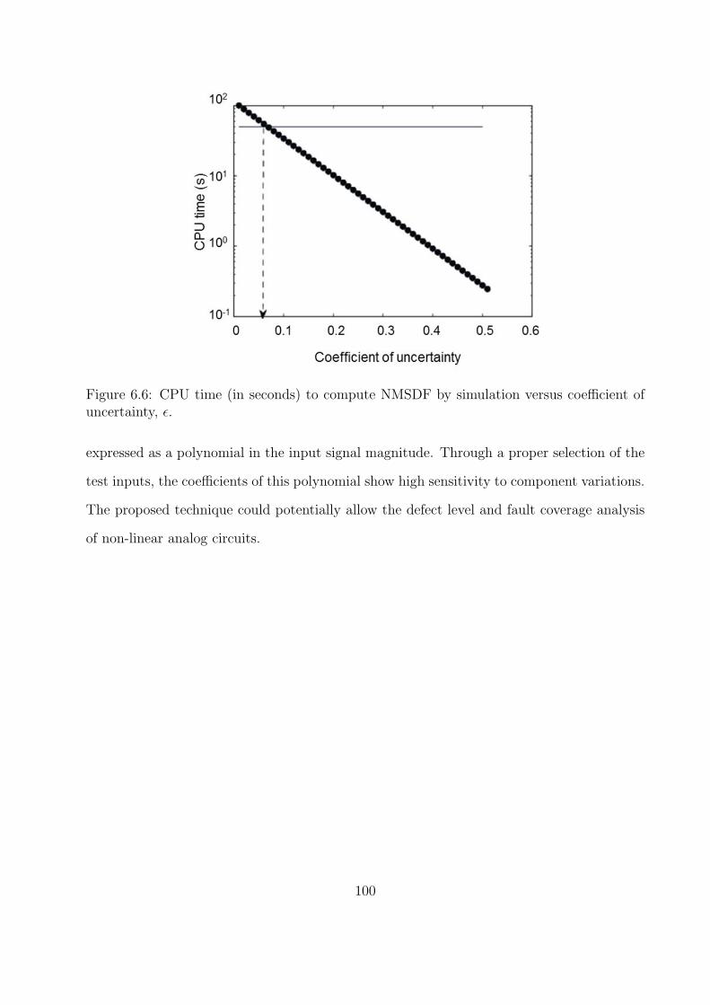
Figure 6.6: CPU time (in seconds) to compute NMSDF by simulation versus coefficient ofuncertainty, ϵ.
expressed as a polynomial in the input signal magnitude. Through a proper selection of the
test inputs, the coefficients of this polynomial show high sensitivity to component variations.
The proposed technique could potentially allow the defect level and fault coverage analysis
of non-linear analog circuits.
100

Chapter 7
Conclusion
Alternate test and fault-model based test methodologies leverage the dependence of out-
puts of the circuit to the variations in circuit components. In this thesis, we proposed circuit
signatures for bolstering both these test methodologies. In particular, we demonstrated para-
metric and catastrophic fault testing in analog circuits using the proposed signatures. The
signatures are based on output’s polynomial function approximation for an input stimulus
swept across the voltage and frequency range; an exponential transformation of coefficients
of the output’s polynomial function approximation; probabilistic moments of the output for
an random input signal (conforming to a known probability density function). Using the
proposed signatures sufficiently small parametric faults of sizes (≈ 5% or more) were un-
covered. The proposed signatures have also been used for diagnosis of both catastrophic
and parametric faults based on sensitivity analysis of the signatures to the circuit compo-
nents. Furthermore, the proposed high-sensitivity test signatures increase the correlation
of RF/analog circuit outputs to specification of the circuit as is desired in alternate test
methodology to minimize yield loss and defect level.
7.1 Thoughts on Future Work
Signatures proposed in this thesis can be used in a closed loop framework such that
the correlation of signatures to circuit specifications is further boosted up. Authors in [138]
propose an adaptive test methodology for analog circuits in the alternate/signature test
framework. Our preliminary studies on this approach have shown the feasibility of this
approach with in conjunction with the signatures such as polynomial coefficients and V-
transform coefficients proposed in the previous chapters.
101

7.1.1 Adaptive Test With Signatures
Block diagram in Figure 7.1 shows the high-level conceptual framework of the adaptive
test methodology using circuit signatures. The circuit-under-test (CUT) is applied with a
carefully crafted stimulus, whose output is then post-processed to generate the signatures
such as polynomial coefficients or V-transform coefficients (proposed in previous chapters).
The signatures are then used to compute correlation with the actual specification based on
actual specification measurement of a small sampling of CUT at run-time. Based on the
prevailing correlation, the input stimulus is tuned to achieve optimally sensitive signatures
that has the highest degree of correlation to the circuit specification.
7.1.2 Preliminary Experiments
To our knowledge, a run-time, closed-loop tuning of the input stimulus to increase
the correlation of the circuit signature to circuit specification for analog circuits has not
been attempted before. Our initial experiments on a sample of 400 LNA circuits show
promising results on the possibility of using such closed-loop tuning on circuit stimulus
to achieve high correlation with specification, which results in lower defect level and yield
loss. Figure 7.3 shows the improved correlation between the signature, in this case, V-
transform of supply current (Idd), as opposed to just Idd and the specification IIP3 (shown
in Figure 7.2). The penalty paid in this process is the extra test-time required to process
the signatures and compute the required adjustments to the input stimulus at run-time (for
example at production). However, it turns out that even minor adjustments in the input
stimulus parameters can give rich dividends in the amount of correlation achieved through
such closed-loop tuning. Furthermore, the computation time required for computing the
change in stimulus along with the time required to initiate the change in the input stimulus
amounts to about 10% increase in the total test-time when compared to test-flows that do
not use such closed form tuning. Table 7.1 shows a comparison of three techniques, namely:
testing for the specification “as is,” using V-transform coefficients in open-loop, and using
102

Figure 7.1: Block diagram of the adaptive test system based on circuit signatures.
Table 7.1: Comparison of defect level, yield loss, and test time for actual specification test,signature test in open loop, and signature test in closed loop.
Test Method Defect Level Yield Loss Test Time (per device)
Actual specification test 0% 0% 15s
Signature test in open loop 8% 12% 100ms
Signature test in closed loop 0.8% 1.8% 105ms
V-transform coefficients in closed-loop. Actual specification testing serves as the baseline
case (or ideal scenario) for defect level (DL) and yield loss (YL). Notice that signatures
taken in open-loop result in a DL and YL of 8% and 12% respectively. Having a closed-loop
tuning of the stimulus improves DL and YL to 0.8% and 1.8% with a 5% time-penalty over
the open-loop case. But both these techniques give close to a 100x improvement in test-time
over the baseline case (of measuring actual specification). More experiments are needed to
study how this procedure would scale when the number of CUT are large and any other
inadequacies of this approach.
103
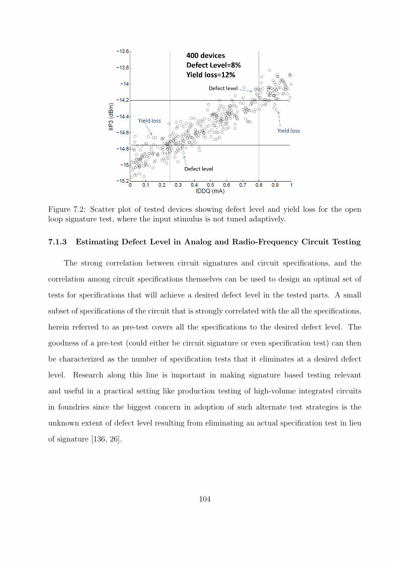
Figure 7.2: Scatter plot of tested devices showing defect level and yield loss for the openloop signature test, where the input stimulus is not tuned adaptively.
7.1.3 Estimating Defect Level in Analog and Radio-Frequency Circuit Testing
The strong correlation between circuit signatures and circuit specifications, and the
correlation among circuit specifications themselves can be used to design an optimal set of
tests for specifications that will achieve a desired defect level in the tested parts. A small
subset of specifications of the circuit that is strongly correlated with the all the specifications,
herein referred to as pre-test covers all the specifications to the desired defect level. The
goodness of a pre-test (could either be circuit signature or even specification test) can then
be characterized as the number of specification tests that it eliminates at a desired defect
level. Research along this line is important in making signature based testing relevant
and useful in a practical setting like production testing of high-volume integrated circuits
in foundries since the biggest concern in adoption of such alternate test strategies is the
unknown extent of defect level resulting from eliminating an actual specification test in lieu
of signature [136, 26].
104

Figure 7.3: Scatter plot of tested devices showing defect level and yield loss for the closedloop signature test, where the input stimulus is tuned adaptively.
105
Bibliography
[1] “International Technology Roadmap for Semiconductors (ITRS) 1999,” Accessed05/11/2013. http://www.itrs.net/Links/2001ITRS/Links/1999 SIA Roadmap/Test.pdf.
[2] “International Technology Roadmap for Semiconductors (ITRS) 2009,” Accessed05/11/2013. http://www.itrs.net/Links/2009ITRS/Home2009.htm.
[3] “NI ELVIS,” Accessed 05/28/2013. http://www.ni.com/ni-elvis/.
[4] “LTspice IV, Linear Technology,” accessed June 23, 2013. http://www.linear.com/designtools/software/.
[5] L. Abdallah, H.-G. Stratigopoulos, S. Mir, and J. Altet, “Testing RF Circuits with TrueNon-Intrusive Built-in Sensors,” in Proc. Design, Automation Test in Europe ConferenceExhibition, 2012, pp. 1090–1095.
[6] A. Abderrahman, E. Cerny, and B. Kaminska, “Optimization Based Multifrequency TestGeneration for Analog Circuits,” Journal of Electronic Testing: Theory and Applications,vol. 9, no. 1-2, pp. 59–73, Mar. 1996.
[7] M. Abramovici, M. A. Breuer, and A. D. Friedman, Digital Systems Testing and TestableDesign. New York, NY: Wiley-IEEE Press, 1994.
[8] E. Acar and S. Ozev, “Defect-Based RF Testing Using a New Catastrophic Fault Model,” inProc. International Test Conf., 2005.
[9] V. D. Agrawal, “An Information Theoretic Approach to Digital Fault Testing,” IEEE Trans.Comput., vol. C-30, no. 8, pp. 582–587, Aug. 1981.
[10] S. S. Akbay, S. Sen, and A. Chatterjee, “Testing RF Components with Supply CurrentSignatures,” in Proc. Asian Test Symposium, Nov. 2007, pp. 393–398.
[11] R. J. Allen, “Failure Prediction Employing Continuous Monitoring Techniques,” IEEE Trans-actions on Aerospace, vol. 1, no. 2, pp. 924–930, 1963.
[12] W. P. M. Allen, D. G. Bailey, S. N. Demidenko, and V. Piuri, “Analysis and Applicationof Digital Spectral Warping in Analog and Mixed-Signal Testing,” IEEE Transactions onReliability, vol. 52, no. 4, pp. 444–457, Dec. 2003.
[13] M. Aminian and F. Aminian, “A Comprehensive Examination of Neural Network Architec-tures for Analog Fault Diagnosis,” in Proc. Int. Joint Conf. Neural Networks, volume 3, 2001,pp. 2304–2309.
[14] K. Arabi, B. Kaminska, and J. Rzeszut, “A New Built-in Self-test Approach For Digital-to-analog And Analog-to-digital Converters,” in Proc. IEEE/ACM Int. Conf. on Computer-Aided Design, 1994, pp. 491–494.
106
[15] F. Azais, Y. Bertrand, M. Renovell, A. Ivanov, and S. Tabatabaei, “An All-Digital DFTScheme for Testing Catastrophic Faults in PLLs,” IEEE Design & Test of Computers, vol. 20,no. 1, pp. 60–67, 2003.
[16] A. Balivada, H. Zheng, N. Nagi, A. Chatterjee, and J. A. Abraham, “A Unified Approachto Fault Simulation of Linear Mixed-Signal Circuits,” Jour. Electronic Testing: Theory andApplications, vol. 9, no. 1, pp. 29–41, Aug. 1996.
[17] J. W. Bandler and A. E. Salama, “Fault Diagnosis of Analog Circuits,” Proceedings of theIEEE, vol. 73, no. 8, pp. 1279–1325, 1985.
[18] M. J. Barragan, R. Fiorelli, G. Leger, A. Rueda, and J. L. Huertas, “Improving the Accuracyof RF Alternate Test Using Multi-VDD Conditions: Application to Envelope-Based Test ofLNAs,” in Proc. 20th IEEE Asian Test Symposium, Nov. 2011, pp. 359–364.
[19] S. D. Bedrosian and D. W. C. Shen, “Adaptive Learning Model for Optimization of AnalogTests,” in Proc. 20th Mid-west Symp. Circuits and Systems, 1977, pp. 206–210.
[20] R. S. Berkowitz, “Conditions for Network-Element-Value Solvability,” IRE Transactions onCircuit Theory, vol. 9, no. 1, pp. 24–29, 1962.
[21] R. S. Berkowitz and P. B. Krishnaswamy, “Computer Techniques for Solving Electric Circuitsfor Fault Isolation,” IEEE Transactions on Aerospace, vol. 1, no. 2, pp. 1090–1099, 1963.
[22] R. S. Berkowitz and R. L. Wexelblat, “Statistical Considerations in Element Value Solutions,”IRE Transactions on Military Electronics, vol. MIL-6, no. 3, pp. 282–288, 1962.
[23] S. Bhunia and K. Roy, “Dynamic Supply Current Testing of Analog Circuits Using WaveletTransform,” in Proc. 20th IEEE VLSI Test Symp., Apr. 2002, pp. 302–307.
[24] S. Biswas and R. D. Blanton, “Statistical Test Compaction Using Binary Decision Trees,”IEEE Design & Test of Computers, vol. 23, no. 6, pp. 452–462, 2006.
[25] S. Biswas, P. Li, R. D. Blanton, and L. T. Pileggi, “Specification Test Compaction for AnalogCircuits and MEMS [Accelerometer and Opamp Examples],” in Proc. Design, Automationand Test in Europe, 2005, pp. 164–169.
[26] A. Bounceur, S. Mir, and H.-G. Stratigopoulos, “Estimation of Analog Parametric Test Met-rics Using Copulas,” IEEE Transactions on Computer-Aided Design of Integrated Circuitsand Systems, vol. 30, no. 9, pp. 1400–1410, 2011.
[27] R. N. Bracewell, The Fourier Transform and Its Applications. McGraw-Hill, 1986.
[28] S. Bracho, M. Martinez, and J. Arguelles, “Current Test Methods in Mixed Signal Circuits,”in Proc. 38th Midwest Symp. Circuits and Systems, volume 2, 1995, pp. 1162–1167.
[29] A. M. Brosa and J. Figueras, “On Maximizing the Coverage of Catastrophic and ParametricFaults,” in Proc. European Test Workshop 1999, 1999, pp. 123–128.
[30] F. D. Brown, N. F. McAllister, and R. P. Perry, “An Application of Inverse Probability toFault Isolation,” IRE Trans. Mil. Electron., vol. MIL-6, no. 1, pp. 260–267, 1962.
[31] J. M. Brown, D. R. Towill, and P. A. Payne, “Predicting Servomechanism Dynamic Errorsfrom Frequency Response Measurements,” Radio and Electronic Engineer, vol. 42, no. 1, pp.7–20, 1972.
[32] M. Burns and G. Roberts, Introduction to Mixed-Signal IC Test and Measurement. OxfordUniversity Press, 2000.
107

[33] M. L. Bushnell and V. D. Agrawal, Essentials of Electronic Testing for Digital, Memory andMixed-Signal VLSI Circuits. Boston: Springer, 2000.
[34] S. Chakrabarty, V. Rajan, J. Ying, M. Mansjur, K. Pattipati, and S. Deb, “A VirtualTest-Bench for Analog Circuit Testability Analysis and Fault Diagnosis,” in Proc. IEEEAUTOTESTCON, 1998, pp. 337–352.
[35] S. Chakravarty and P. J. Thadikaran, Introduction to IDDQ Testing. Springer, 1997.
[36] C.-Y. Chao, H.-J. Lin, and L. Milor, “Fault-Driven Testing of LSI Analog Circuits,” in Proc.35th Midwest Symp. Circuits and Systems, 1992, pp. 927–930.
[37] S. Cherubal and A. Chatterjee, “Test Generation Based Diagnosis of Device Parameters forAnalog Circuits,” in Proc. Design, Automation and Test in Europe Conf., 2001, pp. 596–602.
[38] L. O. Chua, Introduction to Nonlinear Network Theory. McGraw-Hill, 1967.
[39] Y. Deng, Y. He, and Y. Sun, “Fault Diagnosis of Analog Circuits with Tolerances UsingArtificial Neural Networks,” in Proc. IEEE Asia-Pacific Conf. Circuits and Systems, 2000,pp. 292–295.
[40] G. Devarayanadurg and M. Soma, “Analytical Fault Modeling and Static Test Generationfor Analog ICs,” in Proc. Int. Conf. on Computer-Aided Design, Nov. 1994, pp. 44–47.
[41] K. R. Eckersall, P. L. Wrighton, I. M. Bell, B. R. Bannister, and G. E. Taylor, “Testing MixedSignal ASICs Through the Use of Supply Current Monitoring,” in Proc. Third European TestConf., 1993, pp. 385–391.
[42] B. R. Epstein, M. H. Czigler, and S. R. Miller, “Fault Detection and Classification in LinearIntegrated Circuits: An Application of Discrimination Analysis and Hypothesis Testing,”IEEE Trans. Comp. Aided Design, vol. 12, no. 1, pp. 102–113, Jan. 1993.
[43] T.-C. Esteban and C.-M. Jaime, “Computing Symbolic Transfer Functions of Analog Circuitsby Applying Pure Nodal Analysis,” in Proc. 4th IEEE International Caracas Conf. Devices,Circuits and Systems, Apr. 2002, pp. C023 – C1–5.
[44] S. L. Farchy, E. D. Gadzheva, L. H. Raykovska, and T. G. Kouyoumdjiev, “Nullator-NoratorApproach to Analogue Circuit Diagnosis Using General-Purpose Analysis Programmes,” Int.Journal of Circuit Theory and Applications, vol. 23, no. 6, pp. 571–585, Dec. 1995.
[45] J. Figueras, “Possibilities and Limitations of IDDQ Testing in Submicron CMOS,” in Proc.Innovative Systems in Silicon Conf., Oct. 1997, pp. 174–185.
[46] S. Freeman, “Optimum Fault Isolation by Statistical Inference,” IEEE Transactions on Cir-cuits and Systems, vol. 26, no. 7, pp. 505–512, 1979.
[47] W. J. H. Friedman, “Multivariate Adaptive Regression Splines,” Annals Ststistics, vol. 19,pp. 1–141, 1991.
[48] D. D. Gaitonde and D. M. H. Walker, “Hierarchical Mapping of Spot Defects to Catas-trophic Faults-Design and Applications,” IEEE Transactions on Semiconductor Manufac-turing, vol. 8, no. 2, pp. 167–177, 1995.
[49] L. Gefferth, “Fault Identification in Resistive and Reactive Networks,” Int. J. Circuit TheoryAppl., vol. 2, no. 1, pp. 273–277, 1974.
[50] P. Gray, B. Wooley, and R. Brodersen, Analog MOS Integrated Circuits, II. New York, NY:Wiley-IEEE Press, 1989.
108

[51] P. R. Gray, P. Hurst, S. Lewis, and R. G. Meyer, Analysis and Design of Analog IntegratedCircuits. New York, NY: Wiley, 4th edition, 2001.
[52] R. K. Gulati and C. F. Hawkins, IDDQ Testing of VLSI Circuits. Springer, 1993.
[53] Z. Guo and J. Savir, “Analog Circuit Test Using Transfer Function Coefficient Estimates,”in Proc. Int. Test Conf., Oct. 2003, pp. 1155–1163.
[54] Z. Guo, X. M. Zhang, J. Savir, and Y.-Q. Shi, “On Test and Characterization of AnalogLinear Time-Invariant Circuits Using Neural Networks,” in Proc. 10th Asian Test Symp.,2001, pp. 338–343.
[55] A. Halder, S. Bhattacharya, and A. Chatterjee, “Automatic Multitone Alternate Test Gen-eration for RF Circuits Using Behavioral Models,” in Proc. Int. Test Conf., Nov. 2003, pp.665–673.
[56] A. Halder, S. Bhattacharya, and A. Chatterjee, “System-Level Specification Testing Of Wire-less Transceivers,” IEEE Trans. on Very Large Scale Integration (VLSI) Systems, vol. 16,no. 3, pp. 263–276, 2008.
[57] N. B. Hamida and B. Kaminska, “Analog Circuit Testing Based on Sensitivity Computationand New Circuit Modeling,” in Proc. Int. Test Conf., 1993, pp. 652–661.
[58] N. B. Hamida and B. Kaminska, “Multiple Fault Analog Circuit Testing by Sensitivity Anal-ysis,” Journal of Electronic Testing: Theory and Applications, vol. 4, no. 4, pp. 331–343,Nov. 1993.
[59] D. Han and A. Chatterjee, “Simulation-in-the-loop Analog Circuit Sizing Method usingAdaptive Model-based Simulated Annealing,” in Proc. 4th IEEE International Workshopon System-on-Chip for Real-Time Applications, July 2004, pp. 127–130.
[60] W. J. Hankley and H. M. Merrill, “A Pattern Recognition Technique for System ErrorAnalysis,” IEEE Transactions on Reliability, vol. R-20, no. 3, pp. 148–153, 1971.
[61] S. Haykin and B. V. Veen, Signals and Systems. Wiley, 2003.
[62] W. Hochwald and J. Bastian, “A Dc Approach for Analog Fault Dictionary Determination,”IEEE Transactions on Circuits and Systems, vol. 26, no. 7, pp. 523–529, 1979.
[63] C. Holdenried, J. Haslett, J. McRory, R. Beards, and A. Bergsma, “A DC-4 GHz TrueLogarithmic Amplifier: Theory and Implementation,” IEEE Journal of Solid-State Circuits,vol. 37, no. 10, pp. 1290–1299, Oct. 2002.
[64] J. Huanca and R. Spence, “New Statistical Algorithm for Fault Location in TolerancedAnalogue Circuits,” IEE Proceedings Electronic Circuits and Systems Pt. G., vol. 130, no. 6,pp. 243–251, 1983.
[65] P. Kabisatpathy, A. Barua, and S. Sinha, “A Pseudo-Random Testing Scheme for AnalogIntegrated Circuits Using Artificial Neural Network Model-Based Observers,” in Proc. 45thMidwest Symp. on Circuits and Systems, volume 2, 2002.
[66] P. Kabisatpathy, A. Barua, and S. Sinha, Fault Diagnosis of Analog Integrated Circuits.Springer, 2005.
[67] J. Kaderka, V. Musil, J. Povazanec, and P. Simek, “Neural Network Based System for Testingand Diagnostics of Analogue Integrated Circuits,” in Proc. Third IEEE Int. Electronics,Circuits, and Systems Conf., volume 2, 1996, pp. 1198–1201.
109
[68] T. Kailath, Linear Systems. Prentice Hall, 1980.
[69] S. Katz, R. M. H. Cheng, and V. Aula, “Fault Identification in Resistive and ReactiveNetworks,” Int. J. Circuit Theory Appl., vol. 7, no. 1, pp. 399–412, 1979.
[70] R. Kondagunturi, E. Bradley, K. Maggard, and C. Stroud, “Benchmark Circuits for Analogand Mixed-Signal Testing,” in Proc. 20th Int. Conf. on Microelectronics, Mar. 1999, pp.217–220.
[71] J. Kranton and A. Libenson, “A Pattern Recognition Approach to Fault Isolation,” IEEETransactions on Aerosp.-Support Conf. Procedures, vol. AS-1, no. 1, pp. 1320–1326, 1963.
[72] E. Kreyzig, Advanced Engineering Mathematics. Wiley, 2005.
[73] J. Lee and S. D. Bedrosian, “Fault Isolation Algorithm for Analog Electronic Systems usingthe Fuzzy Concept,” IEEE Transactions on Circuits and Systems, vol. 26, no. 7, pp. 518–522,1979.
[74] T. H. Lee, The Design of CMOS Radio-Frequency Integrated Circuits. Cambridge UniversityPress, 1998.
[75] W. L. Lindermeir, H. E. Graeb, and K. J. Antreich, “Analog Testing by CharacteristicObservation Inference,” IEEE Trans. Comp. Aided Design, vol. 23, no. 6, pp. 1353–1368,June 1999.
[76] W. M. Lindermeir, H. E. Graeb, and K. J. Antreich, “Analog Testing by CharacteristicObservation Inference,” IEEE Transactions on Computer-Aided Design of Integrated Circuitsand Systems, vol. 18, no. 9, pp. 1353–1368, 1999.
[77] W. M. Lindermeir, T. J. Vogels, and H. E. Graeb, “Analog Test Design with IDD Measure-ments for the Detection of Parametric and Catastrophic Faults,” in Proc. Design, Automationand Test in Europe, 1998, pp. 822–827.
[78] J. H. Maenpaa, C. J. Stehman, and W. J. Stahl, “Fault Isolation in Conventional LinearSystems: A Progress Report,” IEEE Transactions on Reliability, vol. R-18, no. 1, pp. 12–14,1969.
[79] M. Mahoney, DSP-Based Testing of Analog and Mixed-Signal Circuits. IEEE ComputerSociety Press, 1987.
[80] A. Meixner and W. Maly, “Fault Modeling for the Testing of Mixed Integrated Circuits,” inProc. Int. Test Conference, 1991, pp. 564–572.
[81] H. M. Merrill, “Failure Diagnosis Using Quadratic Programming,” IEEE Transactions onReliability, vol. R-22, no. 4, pp. 207–213, 1973.
[82] L. Milor, “A Tutorial Introduction to Research on Analog and Mixed-Signal Circuit Testing,”IEEE Transactions on Circuits and Systems II: Analog and Digital Signal Processing, vol. 45,no. 10, pp. 1389–1407, Oct. 1998.
[83] L. Milor and A. L. Sangiovanni-Vincentelli, “Optimal Test Set Design for Analog Circuits,”in Proc. IEEE Int. Conf. on Computer-Aided Design, 1990, pp. 294–297.
[84] L. Milor and A. L. Sangiovanni-Vincentelli, “Minimizing Production Test Time to DetectFaults in Analog Circuits,” IEEE Trans. on Computer-Aided Design of Integrated Circuitsand Systems, vol. 13, no. 6, pp. 796–813, 1994.
110

[85] L. Milor and V. Visvanathan, “Detection of Catastrophic Faults in Analog Integrated Cir-cuits,” IEEE Trans. Comp. Aided Design, vol. 8, no. 6, pp. 114–130, June 1989.
[86] S. Mir, H.-G. Stratigopoulos, and A. Bounceur, “Density Estimation for Analog/RF TestProblem Solving,” in Proc. 28th IEEE VLSI Test Symposium, Apr. 2010, p. 41.
[87] C. Morgan, V. Y. Tawfik, and D. R. Towill, “Fault Location in a Noisy Multiple-NonlinearityServosystem,” IEEE Transactions on Circuits and Systems, vol. 26, no. 7, pp. 586–589, 1979.
[88] C. Morgan and D. R. Towill, “Application of the Multiharmonic Fourier Filter to NonlinearSystem Fault Location,” IEEE Transactions on Instrumentation and Measurement, vol. 26,no. 2, pp. 164–169, 1977.
[89] K. Nadesalingam and D. R. Towill, “Frequency Domain Fault Detection and Diagnosis inHybrid Control Systems: A Feasibility Study,” IEEE Transactions on Instrumentation andMeasurement, vol. 27, no. 2, pp. 193–199, 1978.
[90] N. Nagi, A. Chatterjee, A. Balivada, and J. A. Abraham, “Fault-Based Automatic TestGenerator for Linear Analog Devices,” in Proc. Int. Conf. Computer Aided Design, May1993, pp. 88–91.
[91] T. Ozawa, Analog Methods for Computer-Aided Circuit Analysis and Diagnosis. MarcelDekker, 1988.
[92] C.-Y. Pan and K.-T. Cheng, “Test Generation for Linear Time-Invariant Analog Circuits,”IEEE Trans. Circuits and Systems II: Analog and Digital Signal Processing, vol. 46, no. 5,pp. 554–564, May 1999.
[93] V. Panic, D. Milovanovic, P. Petkovic, and V. Litovski, “Fault Location in Passive AnalogRC Circuits by measuring Impulse Response,” in Proc. 20th Int. Conf. on Microelectronics,Sept. 1995, pp. 12–14.
[94] A. Papoulis, Probability, Random Variables, and Stochastic Processes. McGraw-Hill, 1965.
[95] J. Park, J. Chung, and J. A. Abraham, “LFSR-Based Performance Characterization of Non-linear Analog and Mixed-Signal Circuits,” in Proc. IEEE Asian Test Symposium, Nov. 2009,pp. 373–378.
[96] J. Park, H. Shin, and J. A. Abraham, “Pseudorandom Test for Nonlinear Circuits Basedon a Simplified Volterra Series Model,” in Proc. 8th IEEE International Symp. on QualityElectronic Design, Mar. 2007, pp. 495–500.
[97] W. A. Plice, “Overview of Current Automated Analog Test Design,” in Proc. IEEE TestSemiconductor Conf., Nov. 1979, pp. 128–136.
[98] T. L. Quarles, D. O. Pederson, A. R. Newton, A. L. Sangiovanni-Vincentelli, C. Wayne,and J. M. Rabaey, “The Spice Page,” accessed June 23, 2013. http://bwrcs.eecs.berke-ley.edu/Classes/IcBook/SPICE/.
[99] R. Rajsuman, IDDQ Testing for CMOS VLSI. Artech House, 1995.
[100] R. Ramadoss and M. L. Bushnell, “Test Generation for Mixed-Signal Devices Using SignalFlow Graphs,” in Proc. 9th Int. Conf. on VLSI Design, Jan. 1996, pp. 242–248.
[101] R. Ramadoss and M. L. Bushnell, “Test Generation for Mixed-Signal Devices Using SignalFlow Graphs,” Journal of Electronic Testing: Theory and Applications, vol. 14, no. 3, pp.189–205, June 1999.
111

[102] M. Ransom and R. Saeks, “Fault Isolation with Insufficient Measurements,” IEEE Transac-tions on Circuit Theory, vol. 20, no. 4, pp. 416–417, 1973.
[103] B. Razavi, Design of Analog CMOS Integrated Circuits. McGraw-Hill, 2001.
[104] B. Razavi, RF Microelectronics. Prentice Hall, 2011.
[105] S. C. D. Roy, “Single Shunt Fault Diagnosis in a Resistive Ladder,” IEEE Transactions onInstrumentation and Measurement, vol. IM-30, no. 2, pp. 143–146, 1981.
[106] L. M. Roytman and M. N. S. Swamy, “Criteria for Analog Fault Diagnosis,” in Proc. EuropeanConf. Circuit Theory and Design, 1981, pp. 75–78.
[107] R. A. Rutenbar, “Design for Leading-Edged Mixed-Signal ICs Analog IntellectualProperty: Why, When, How,” Accessed 05/11/2013. http://www.hotchips.org/wp-content/uploads/hc archives/hc13/1 Sun/t2a-rutenbar.pdf.
[108] R. Saeks, “An Experiment in Fault Prediction–II,” in Proc. Int. Automatic Testing Conf.AUTOTESTCON, 1976, p. 53.
[109] R. Saeks, “An Approach to Built-In Testing,” IEEE Transactions on Aerospace and Elec-tronic Systems, vol. AES-14, no. 5, pp. 813–818, 1978.
[110] A. E. Salama, J. A. Starzyk, and J. W. Bandler, “A Review of Analog Automatic TestGeneration,” in Proc. Int. Automatic Testing Conf. AUTOTESTCON, 1978, pp. 1–8.
[111] J. Savir and Z. Guo, “Test Limitations of Parametric Faults in Analog Circuits,” inProc. IEEE 11th Asian Test Symp., 2002, pp. 39–44.
[112] K. B. Schaub and J. Kelly, Production Testing of RF and System-on-a-Chip Devices forWireless Communications. Artech House, 2004.
[113] H. H. Schreiber, “Fault Dictionary Based upon Stimulus Design,” IEEE Transactions onCircuits and Systems, vol. 26, no. 7, pp. 529–537, 1979.
[114] S. Seshu and R. Waxman, “Fault Isolation in Conventional Linear Systems–A FeasibilityStudy,” IEEE Transactions on Reliability, vol. R-15, no. 1, pp. 11–16, 1966.
[115] N. Shanbhag, K. Soumyanath, and S. Martin, “Reliable Low-Power Design in the Presenceof Deep Submicron Noise,” in Proc. Int. Symp. Low Power Electronics and Design, 2000, pp.295–302.
[116] N. R. Shanbhag, “A Fundamental Basis for Power-Reduction in VLSI Circuits,” in Proc.IEEE Int. Symp. Circuits and Systems, volume 4, 1996, pp. 9–12.
[117] S. Sindia, V. D. Agrawal, and F. F. Dai, “LNA Test: A Polynomial Coeffi-cient Approach,” in Proc. North Atlantic Test Workshop, 2011, Accessed 05/27/2013.http://www.eng.auburn.edu/∼agrawvd/TALKS/NATW11/LNA test.pdf.
[118] S. Sindia, V. D. Agrawal, and V. Singh, “Distinguishing Process Variation Induced Faultsfrom Manufacturing Defects in Analog Circuits using V-Transform Coefficients,” in Proc.43rd IEEE Southeastern Symposium on System Theory, Mar. 2011, pp. 231–236.
[119] S. Sindia, V. D. Agrawal, and V. Singh, “Non-linear Analog Circuit Test and Diagnosisunder Process Variation using V-Transform Coefficients,” in Proc. 29th IEEE VLSI TestSymposium, May 2011, pp. 64–69.
112
[120] S. Sindia, V. D. Agrawal, and V. Singh, “Testing Linear and Non-linear Analog Circuitsusing Moment Generating Functions,” in Proc. 12th IEEE Latin American Test Workshop,Mar. 2011, pp. 1–6.
[121] S. Sindia, V. D. Agrawal, and V. Singh, “Defect Level and Fault Coverage in CoefficientBased Analog Circuit Testing,” Journal of Electronic Testing: Theory and Applications,vol. 28, no. 4, pp. 541–549, Aug. 2012.
[122] S. Sindia, V. D. Agrawal, and V. Singh, “Parametric Fault Testing of Non-Linear AnalogCircuits Based on Polynomial and V-Transform Coefficients,” Journal of Electronic Testing:Theory and Applications, vol. 28, no. 5, pp. 757–771, Oct. 2012.
[123] S. Sindia, V. Singh, and V. D. Agrawal, “Bounds on Defect Level and Fault Coverage inLinear Analog Circuit Testing,” in Proc. 13th VLSI Design and Test Symp., July 2009, pp.410–421.
[124] S. Sindia, V. Singh, and V. D. Agrawal, “Multi-Tone Testing of Linear and Nonlinear AnalogCircuits Using Polynomial Coefficients,” in Proc. 18th IEEE Asian Test Symposium, Nov.2009, pp. 63–68.
[125] S. Sindia, V. Singh, and V. D. Agrawal, “Polynomial Coefficient Based DC Testing of Non-Linear Analog Circuits,” in Proc. 19th ACM Great Lakes Symp. on VLSI, May 2009, pp.69–74.
[126] S. Sindia, V. Singh, and V. D. Agrawal, “Polynomial Coefficient Based Multi-Tone Testingof Analog Circuits,” in Proc. North Atlantic Test Workshop, May 2009, pp. 9–18.
[127] S. Sindia, V. Singh, and V. D. Agrawal, “V-Transform: An Enhanced Polynomial CoefficientBased DC Test for Non-Linear Analog Circuits,” in Proc. of 8th IEEE East West Design &Test Symposium, Sept. 2009, pp. 283–286.
[128] S. Sindia, V. Singh, and V. D. Agrawal, “Parametric Fault Diagnosis of Nonlinear AnalogCircuits Using Polynomial Coefficients,” in Proc. 23rd International Conference on VLSIDesign, Jan. 2010, pp. 288–293.
[129] M. Slamani and B. Kaminska, “Analog Circuit Fault Diagnosis Based on Sensitivity Compu-tation and Functional Testing,” IEEE Design & Test of Computers, vol. 19, no. 1, pp. 30–39,1992.
[130] R. Spina and S. Upadhyaya, “Fault Diagnosis of Analog Circuits Using Artificial NeuralNetworks as Signature Analyzers,” in Proc. Fifth Annual IEEE Int. ASIC Conf. and Exhibit,1992, pp. 355–358.
[131] R. Spina and S. Upadhyaya, “Linear Circuit Fault Diagnosis using Neuromorphic Analyzers,”IEEE Transactions on Circuits and Systems II: Analog and Digital Signal Processing, vol. 44,no. 3, pp. 188–196, 1997.
[132] H. Sriyananda and D. R. Towill, “Fault Diagnosis Using Time Domain Measurements,” Radioand Electronic Engineer, vol. 43, no. 9, pp. 523–533, 1973.
[133] H. Sriyananda, D. R. Towill, and J. H. Williams, “Voting Techniques for Fault Diagnosisfrom Frequency-Domain Test-Data,” IEEE Transactions on Reliability, vol. R-24, no. 4, pp.260–267, 1975.
[134] V. Stopjakova, P. Malosek, M. Matej, V. Nagy, and M. Margala, “Defect Detection in Analogand Mixed Circuits by Neural Networks using Wavelet Analysis,” IEEE Transactions onReliability, vol. 54, no. 3, pp. 441–448, 2005.
113
[135] V. Stopjakova, D. Micusik, L. Benuskova, and M. Margala, “Neural Networks-Based Para-metric Testing of Analog IC,” in Proc. 17th IEEE Int. Symp. Defect and Fault Tolerance inVLSI Systems, 2002, pp. 408–416.
[136] H.-G. Stratigopoulos, “Test Metrics Model for Analog Test Development,” IEEE Trans-actions on Computer-Aided Design of Integrated Circuits and Systems, vol. 31, no. 7, pp.1116–1128, 2012.
[137] H.-G. Stratigopoulos and Y. Makris, “Error Moderation in Low-Cost Machine-Learning-Based Analog/RF Testing,” IEEE Transactions on Computer-Aided Design of IntegratedCircuits and Systems, vol. 27, no. 2, pp. 339–351, 2008.
[138] H.-G. Stratigopoulos and S. Mir, “Adaptive Alternate Analog Test,” IEEE Design & Test ofComputers, vol. 29, no. 4, pp. 71–79, 2012.
[139] H.-G. Stratigopoulos, S. Mir, E. Acar, and S. Ozev, “Defect Filter for Alternate RF Test,”in Proc. 14th IEEE European Test Symp., 2009, pp. 101–106.
[140] H.-G. Stratigopoulos, S. Mir, and A. Bounceur, “Evaluation of Analog/RF Test Measure-ments at the Design Stage,” IEEE Transactions on Computer-Aided Design of IntegratedCircuits and Systems, vol. 28, no. 4, pp. 582–590, 2009.
[141] S. Sunter and N. Nagi, “Test Metrics for Analog Parametric Faults,” in Proc. 17th IEEEVLSI Test Symposium, Apr. 1999, pp. 226–234.
[142] J. C. Sutton-III, “Identification of Electronic Component Faults Using Neural Networksand Fuzzy Systems,” in Proc. Int. Industrial Electronics, Control, Instrumentation, andAutomation Power Electronics and Motion Control Conf., 1992, pp. 1466–1471.
[143] M. Tadeusiewicz and S. Halgas, “An Efficient Method for Simulation of Multiple CatastrophicFaults,” in Proc. 15th IEEE Int. Conf. Electronics, Circuits and Systems, 2008, pp. 356–359.
[144] C. Tinaztepe and N. S. Prywes, “Generation of Software for Computer Controlled TestEquipment for Testing Analog Circuits,” IEEE Transactions on Circuits and Systems, vol. 26,no. 7, pp. 537–548, 1979.
[145] M. F. Toner and G. W. Roberts, “On the Practical Implementation of Mixed Analog-DigitalBIST,” in Proc. Custom Integrated Circuits Conference, May 1995, pp. 525–528.
[146] K. Y. Tong, “Single Fault Location in a Linear Analogue System with Variable SensitivityMatrix,” Electronics Letters, vol. 16, no. 6, pp. 221–222, 1980.
[147] D. R. Towill, “Dynamic Testing of Control Systems,” Radio and Electronic Engineer, vol. 47,no. 11, pp. 505–521, 1977.
[148] D. R. Towill and P. A. Payne, “Frequency Domain Approach to Automatic Testing of ControlSystems,” Radio and Electronic Engineer, vol. 41, no. 2, pp. 51–60, 1971.
[149] L. Tung and R. Saeks, “An Experiment in Fault Prediction,” in Proc. 4th Symp. Reliabilityin Electronics, 1977, pp. 249–257.
[150] K. C. Varghese, H. J. Williams, and D. R. Towill, “Simplified ATPG and Analog FaultLocation via a Clustering and Separability Technique,” IEEE Transactions on Circuits andSystems, vol. 26, no. 7, pp. 496–505, 1979.
[151] P. N. Variyam, S. Cherubal, and A. Chatterjee, “Prediction of Analog Performance Param-eters Using Fast Transient Testing,” IEEE Trans. on Computer-Aided Design of IntegratedCircuits and Systems, vol. 21, no. 3, pp. 349–361, 2002.
114

[152] W. Verhaegen and G. Gielen, “Efficient Symbolic Analysis of Analog Integrated CircuitsUsing Determinant Decision Diagrams,” in Proc. IEEE Int. Conf. Electronics, Circuits andSystems, Sept. 1998, pp. 89–92.
[153] B. Vinnakota, Introduction to Mixed-Signal IC Test and Measurement. Prentice-Hall PTR,1998.
[154] R. Voorakaranam, S. S. Akbay, S. Bhattacharya, S. Cherubal, and A. Chatterjee, “SignatureTesting of Analog and RF Circuits: Algorithms and Methodology,” IEEE Trans. on Circuitsand Systems I: Regular Papers, vol. 54, no. 5, pp. 1018–1031, 2007.
[155] R. Voorakaranam and A. Chatterjee, “Test Generation for Accurate Prediction of AnalogSpecifications,” in Proc. 18th IEEE VLSI Test Symposium, Apr. 2000, pp. 137–142.
[156] R. Voorakaranam, S. Cherubal, and A. Chatterjee, “A Signature Test Framework for RapidProduction Testing of RF Circuits,” in Proc. Design, Automation and Test in Europe Con-ference and Exhibition, 2002, pp. 186–191.
[157] Y. Xing, “Defect-Oriented Testing of Mixed-Signal ICs: Some Industrial Experience,” inProc. Int. Test Conference, Oct. 1998, pp. 678–687.
[158] V. Zagursky, N. Semyonova, and M. Sirovatkina, “A Histogram Method for Analog-DigitalConverters Testing in Time and Spectral Domain,” in Proc. European Design and Test Con-ference, Mar. 1995, p. 607.
115

Appendix A
Some Theorems on Nonlinear Systems
Theorem A.1 If coefficient ai is a monotonic function of all parameters, then ai takes its
limit (maximum and minimum) values when at least one or more of the parameters are at
the boundaries of their individual hypercube.
Proof. Let ai be a function of three parameters say x, y and z. Let ai reach its maximum
value for (x0, y0, z0). Further let x0, y0 = α. Now if we can show that the maximum value of
the coefficient ai occurs at z0 = α we have proved the theorem. From definition of monotonic
dependence of ai on circuit parameters, (A.1) follows.
ai(x0, y0, α) ≥ ai(x0, y0, z0) ∀z0 ≤ α (A.1)
As the maximum value taken by z = α, it follows that z0 = α. With similar arguments we
can show that the minimum value for coefficient occurs when z0 = −α. Hence the statement
of theorem follows.
Theorem A.2 In polynomial expansion of Non-Linear Analog circuit there exists at least
one coefficient that is a monotonic function of all the circuit parameters.
Proof. Consider the block diagram in Figure A.1 which models an 2nth order Non-
Linear analog circuit. x is applied input and y is the response, a1 · · · an are input summed
at each stage. The coefficient corresponding to input x raised to the 2nth power is given by
G in (A.2).
G =n∏
i=1
g2ii (A.2)
116

x
g1
(.)2
x+
a1
x
g2
(.)2+
a2
x
gn
(.)2+
an
y…
Figure A.1: A possible system model for a non-linear circuit.
where gi ∀i = 1 . . . n are the monotonic gains of individual stages in the cascaded blocks.
As the product of two or more monotonic functions is also monotonic we have G to be a
monotonic function. G constitutes the coefficient of the nth power of x in this expansion, as
it lies in the main signal flow path from input to output. Thus it is proved that there is at
least one monotonically varying coefficient in a polynomial expansion of a non-linear analog
circuit. Further, in general the coefficient of 2nth power of such a polynomial expansion is
monotonic.
Theorem A.3 A continuous non-monotonic function f : ℜ → ℜ can be decomposed into
piecewise monotonic functions of the form:
f(x) = f(x)u(x0 − x) + f(x) (u(x− x0)− u(x− x1))+
f(x) (u(x− x1)− u(x− x2)) + · · ·
+f(x) (u(x− xn−1)− u(x− xn))
(A.3)
where x0, x1, · · · xn are all stationary points of f(x) and
u(x) =
1 ∀ x ≥ 0
0 ∀ x < 0
Proof. By Rolle’s theorem [72], if f : ℜ → ℜ is any continuous and differentiable
function in the open interval (a, b) and f(a) = f(b), then there exists c ∈ (a, b) such that
f ′(c) = 0. To extend this result, suppose f(x) is increasing in the interval (a, c−), that is
f ′(x) > 0 ∀x ∈ (a, c−) and decreasing in the interval (c+, b) that is f ′(x) < 0 ∀x ∈ (c+, b)
then at point c, f ′(c) = 0. In general for a continuous function f over arbitrary interval
117
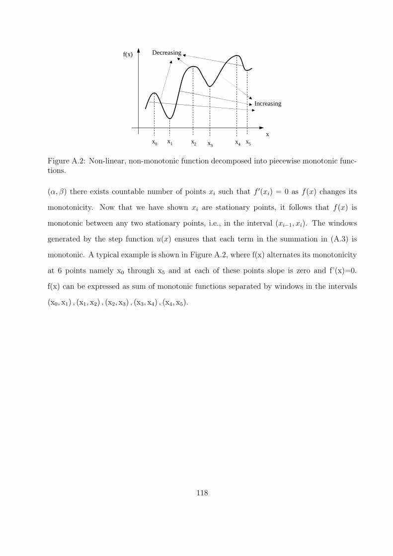
x0 x1 x2 x3x4 x5
x
f(x) Decreasing
Increasing
Figure A.2: Non-linear, non-monotonic function decomposed into piecewise monotonic func-tions.
(α, β) there exists countable number of points xi such that f ′(xi) = 0 as f(x) changes its
monotonicity. Now that we have shown xi are stationary points, it follows that f(x) is
monotonic between any two stationary points, i.e., in the interval (xi−1, xi). The windows
generated by the step function u(x) ensures that each term in the summation in (A.3) is
monotonic. A typical example is shown in Figure A.2, where f(x) alternates its monotonicity
at 6 points namely x0 through x5 and at each of these points slope is zero and f’(x)=0.
f(x) can be expressed as sum of monotonic functions separated by windows in the intervals
(x0, x1) , (x1, x2) , (x2, x3) , (x3, x4) , (x4, x5).
118

Appendix B
Output Variance of RC Filter
R
C vovin
Figure B.1: First order RC low-pass filter.
We use the frequency domain approach to find the transformed RV for Gaussian noise
input excitation of a first order RC filter of Figure B.1. The transfer function of that filter
is given by
H(s) =Vo(s)
Vi(s)=
1
sRC + 1=⇒ |H(jω)|2 =
1
(ωRC)2 + 1(B.1)
With white noise as the input, the discrete values are sampled Gaussian RV of zero mean
and variance = No
2. The output of this filter which is the filtered response is given by vo and
its frequency domain expression is given by
|Vo(jω)|2 =1
(ωRC)2 + 1|Vi(jω)|2 (B.2)
To compute the effective second order moment we integrate this output over all frequencies,
i.e., ω = (0,∞).
µ2 =
∫ ∞
0
(dω
(ωRC)2 + 1
)No
2
=1
RC
No
2arctan(ωRC)|∞0 =
Noπ
4RC(B.3)
119