Embed Size (px)
Citation preview
TJA1441High-speed CAN transceiverRev. 2 — 15 October 2021 Product data sheet
1 General description
The TJA1441 is a member of the TJA144x family of transceivers that provide an interfacebetween a Controller Area Network (CAN) or CAN FD (Flexible Data rate) protocolcontroller and the physical two-wire CAN bus. TJA144x transceivers implement the CANphysical layer as defined in ISO 11898-2:2016 and SAE J2284-1 to SAE J2284-5, andare fully interoperable with high-speed Classical CAN and CAN FD transceivers. AllTJA144x variants enable reliable communication in the CAN FD fast phase at data ratesup to 5 Mbit/s.
The TJA1441 is intended as a simple replacement for high-speed Classical CANand CAN FD transceivers, such as the TJA1051 or TJA1057 from NXP. It offers pincompatibility and is designed to avoid changes to hardware and software design,allowing the TJA1441 to be easily retrofitted to existing applications.
An AEC-Q100 Grade 0 variant, the TJR1441, is available for high temperatureapplications, supporting operation at 150 °C ambient temperature. A variant intended forindustrial applications, the TJF1441, is also available.
1.1 TJA1441 variantsThe TJA1441 comes in three variants, each available in an SO8 or HVSON8 package:
• The TJA1441A is a high-speed CAN transceiver with Normal and Silent modes and aVIO supply pin. The VIO pin allows for direct interfacing with 3.3 V and 5 V-suppliedmicrocontrollers.
• The TJA1441B is a high-speed CAN transceiver with Normal and Silent modes.• The TJA1441D is a high-speed CAN transceiver with Normal and Silent modes with a
transmitter/receiver On/Off input.
2 Features and benefits
2.1 General• ISO 11898-2:2016, SAE J2284-1 to SAE J2284-5 and SAE J1939-14 compliant• Standard CAN and CAN FD data bit rates up to 5 Mbit/s• Low Electromagnetic Emission (EME) and high Electromagnetic Immunity (EMI)• Qualified according to AEC-Q100 Grade 1• Silent mode for node diagnosis and failure containment• TJA1441A only: VIO input for interfacing with 3.3 V to 5 V microcontrollers• TJA1441D only: dedicated input for switching to very low-current Off mode and
disengaging from the bus• All variants are available in SO8 and leadless HVSON8 (3.0 mm x 3.0 mm) packages;
HVSON8 with improved Automated Optical Inspection (AOI) capability.
NXP Semiconductors TJA1441High-speed CAN transceiver
• Dark green product (halogen free and Restriction of Hazardous Substances (RoHS)compliant)
2.2 Predictable and fail-safe behavior• Undervoltage detection with defined handling on all supply pins• Full functionality guaranteed from the undervoltage detection thresholds up to the
maximum limiting voltage values• Defined behavior below the undervoltage detection thresholds• Transceiver disengages from the bus (high-ohmic) when the supply voltage drops
below the Off mode threshold• Internal biasing of TXD and mode selection input pins, to enable defined fail-safe
behavior
2.3 Protection• High ESD handling capability on the bus pins (8 kV IEC and HBM)• Bus pins protected against transients in automotive environments• Transmit Data (TXD) dominant time-out function• Thermally protected
TJA1441 All information provided in this document is subject to legal disclaimers. © NXP B.V. 2021. All rights reserved.
Product data sheet Rev. 2 — 15 October 20212 / 33
NXP Semiconductors TJA1441High-speed CAN transceiver
3 Quick reference data
Symbol Parameter Conditions Min Typ Max Unit
VCC supply voltage 4.5 - 5.5 V
Normal mode, dominant - 38 60 mA
Normal mode, recessive - 4 7 mA
Silent mode - 3 6 mA
ICC supply current
Off mode (TJA1441D only) - 90 250 μA
Vuvd(VCC) undervoltage detection voltageon pin VCC
4 - 4.5 V
Vuvhys(VCC) undervoltage hysteresis voltageon pin VCC
50 - - mV
Vuvd(swoff)(VCC) switch-off undervoltage detectionvoltage on pin VCC
TJA1441B/D 2.65 - 2.95 V
VIO supply voltage on pin VIO 2.95 - 5.5 V
Normal mode, dominant; VTXD = 0 V - 250 760 µA
Normal mode, recessive; VTXD = VIO - 150 460 µA
IIO supply current on pin VIO
Silent mode; VTXD = VIO - 70 200 µA
Vuvd(swoff)(VIO) switch-off undervoltage detectionvoltage on pin VIO
TJA1441A 2.65 - 2.95 V
VESD electrostatic discharge voltage IEC 61000-4-2 on pins CANH and CANL -8 - +8 kV
VCANH voltage on pin CANH limiting value according to IEC 60134 -36 - +40 V
VCANL voltage on pin CANL limiting value according to IEC 60134 -36 - +40 V
Tvj virtual junction temperature -40 - +150 °C
Table 1. Quick reference data
TJA1441 All information provided in this document is subject to legal disclaimers. © NXP B.V. 2021. All rights reserved.
Product data sheet Rev. 2 — 15 October 20213 / 33
NXP Semiconductors TJA1441High-speed CAN transceiver
4 Ordering information
PackageType number
Name Description Version
TJA1441AT
TJA1441BT
TJA1441DT
SO8 plastic small outline package; 8 leads; body width 3.9 mm SOT96-1
TJA1441ATK
TJA1441BTK
TJA1441DTK
HVSON8 plastic thermal enhanced very thin small outline package; noleads; 8 terminals; body 3 × 3 × 0.85 mm
SOT782-1
Table 2. Ordering information
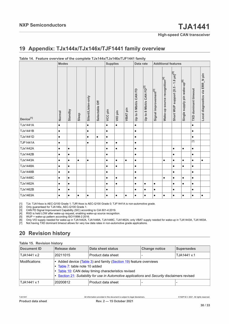
See Section 19 for a feature overview of the complete TJx144x/TJx146x/TJF1441 family.
Modes Supplies Data rate Additional features
Device[1]
Nor
mal
Stan
dby
Slee
p
Sile
nt/L
iste
n-on
ly
Sele
ctab
le O
ff
VCC
pin
VIO
pin
VBAT
pin
Up
to 5
Mbi
t/s C
AN
FD
Up
to 8
Mbi
t/s C
AN
FD
Sign
al im
prov
emen
t[2]
Wak
e-up
sou
rce
reco
gniti
on[3
]
Shor
t WU
P su
ppor
t [0.
5 - 1
.8 µ
s][4
]
Sing
le s
uppl
y pi
n w
ake-
up
TXD
dom
inan
t tim
eout
Loca
l dia
gnos
tics
via
ERR
_N p
inTJA1441A
TJA1441B
TJA1441D
Table 3. TJA1441 feature overview
[1] TJA1441 is AEC-Q100 Grade 1.[2] CAN FD Signal Improvement Capability (SIC) according to CiA 601-4:2019.[3] RXD is held LOW after wake-up request, enabling wake-up source recognition.[4] WUP = wake-up pattern according ISO11898-2:2016.
TJA1441 All information provided in this document is subject to legal disclaimers. © NXP B.V. 2021. All rights reserved.
Product data sheet Rev. 2 — 15 October 20214 / 33
NXP Semiconductors TJA1441High-speed CAN transceiver
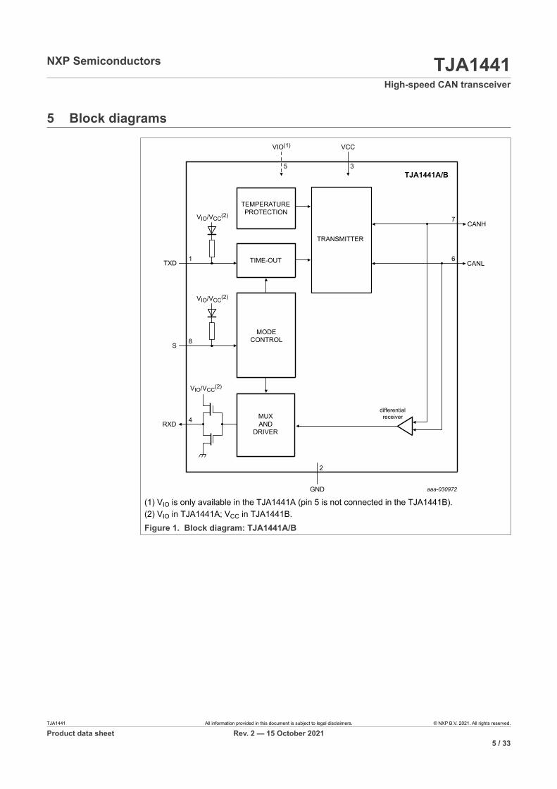
5 Block diagrams
TEMPERATUREPROTECTION
TIME-OUT
MODECONTROL
TXD 1
TRANSMITTER
7
6
2
GND
TJA1441A/B
S 8
aaa-030972
VIO/VCC(2)
VIO/VCC(2)
MUXAND
DRIVERRXD 4
VIO/VCC(2)
3
VCC
5
VIO(1)
CANL
CANH
differentialreceiver
(1) VIO is only available in the TJA1441A (pin 5 is not connected in the TJA1441B).(2) VIO in TJA1441A; VCC in TJA1441B.Figure 1. Block diagram: TJA1441A/B
TJA1441 All information provided in this document is subject to legal disclaimers. © NXP B.V. 2021. All rights reserved.
Product data sheet Rev. 2 — 15 October 20215 / 33
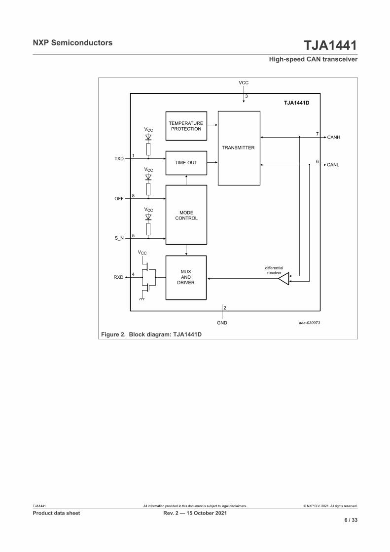
NXP Semiconductors TJA1441High-speed CAN transceiver
TEMPERATUREPROTECTION
TIME-OUT
MODECONTROL
TXD 1
TRANSMITTER
7
6
2
GND
TJA1441D
aaa-030973
VCC
OFF 8
VCC
MUXAND
DRIVERRXD 4
VCC
S_N 5
VCC
3
VCC
CANL
CANH
differentialreceiver
Figure 2. Block diagram: TJA1441D
TJA1441 All information provided in this document is subject to legal disclaimers. © NXP B.V. 2021. All rights reserved.
Product data sheet Rev. 2 — 15 October 20216 / 33
NXP Semiconductors TJA1441High-speed CAN transceiver
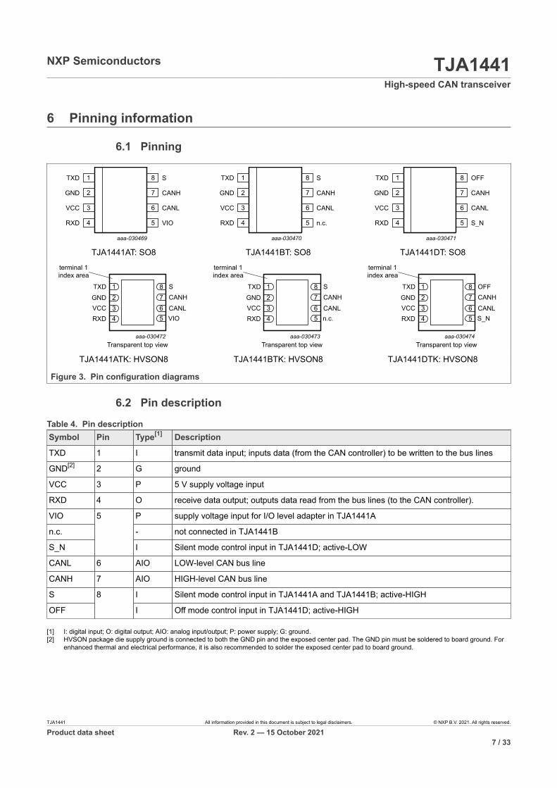
6 Pinning information
6.1 Pinning
TXD S
GND CANH
VCC CANL
RXD VIO
1
2
3
4
6
5
8
7
aaa-030469
TXD S
GND CANH
VCC CANL
RXD n.c.
1
2
3
4
6
5
8
7
aaa-030470
TXD OFF
GND CANH
VCC CANL
RXD S_N
1
2
3
4
6
5
8
7
aaa-030471
TJA1441AT: SO8 TJA1441BT: SO8 TJA1441DT: SO8
RXD 4VCC 3GND 2TXD 1
VIO5CANL6CANH7S8
aaa-030472
terminal 1index area
Transparent top view
RXD 4VCC 3GND 2TXD 1
n.c.5CANL6CANH7S8
aaa-030473
terminal 1index area
Transparent top view
RXD 4VCC 3GND 2TXD 1
S_N5CANL6CANH7OFF8
aaa-030474
terminal 1index area
Transparent top view
TJA1441ATK: HVSON8 TJA1441BTK: HVSON8 TJA1441DTK: HVSON8
Figure 3. Pin configuration diagrams
6.2 Pin description
Symbol Pin Type[1] Description
TXD 1 I transmit data input; inputs data (from the CAN controller) to be written to the bus lines
GND[2] 2 G ground
VCC 3 P 5 V supply voltage input
RXD 4 O receive data output; outputs data read from the bus lines (to the CAN controller).
VIO P supply voltage input for I/O level adapter in TJA1441A
n.c. - not connected in TJA1441B
S_N
5
I Silent mode control input in TJA1441D; active-LOW
CANL 6 AIO LOW-level CAN bus line
CANH 7 AIO HIGH-level CAN bus line
S I Silent mode control input in TJA1441A and TJA1441B; active-HIGH
OFF
8
I Off mode control input in TJA1441D; active-HIGH
Table 4. Pin description
[1] I: digital input; O: digital output; AIO: analog input/output; P: power supply; G: ground.[2] HVSON package die supply ground is connected to both the GND pin and the exposed center pad. The GND pin must be soldered to board ground. For
enhanced thermal and electrical performance, it is also recommended to solder the exposed center pad to board ground.
TJA1441 All information provided in this document is subject to legal disclaimers. © NXP B.V. 2021. All rights reserved.
Product data sheet Rev. 2 — 15 October 20217 / 33
NXP Semiconductors TJA1441High-speed CAN transceiver
7 Functional description
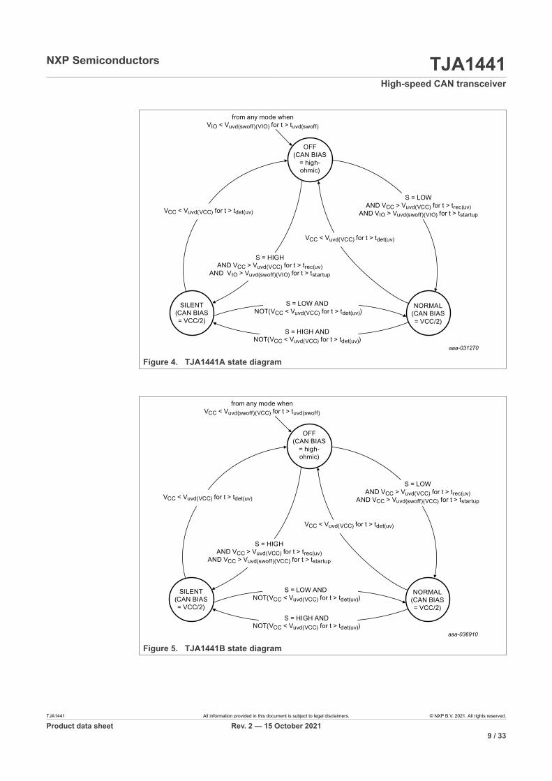
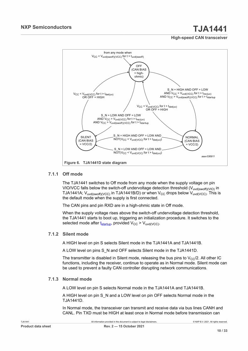
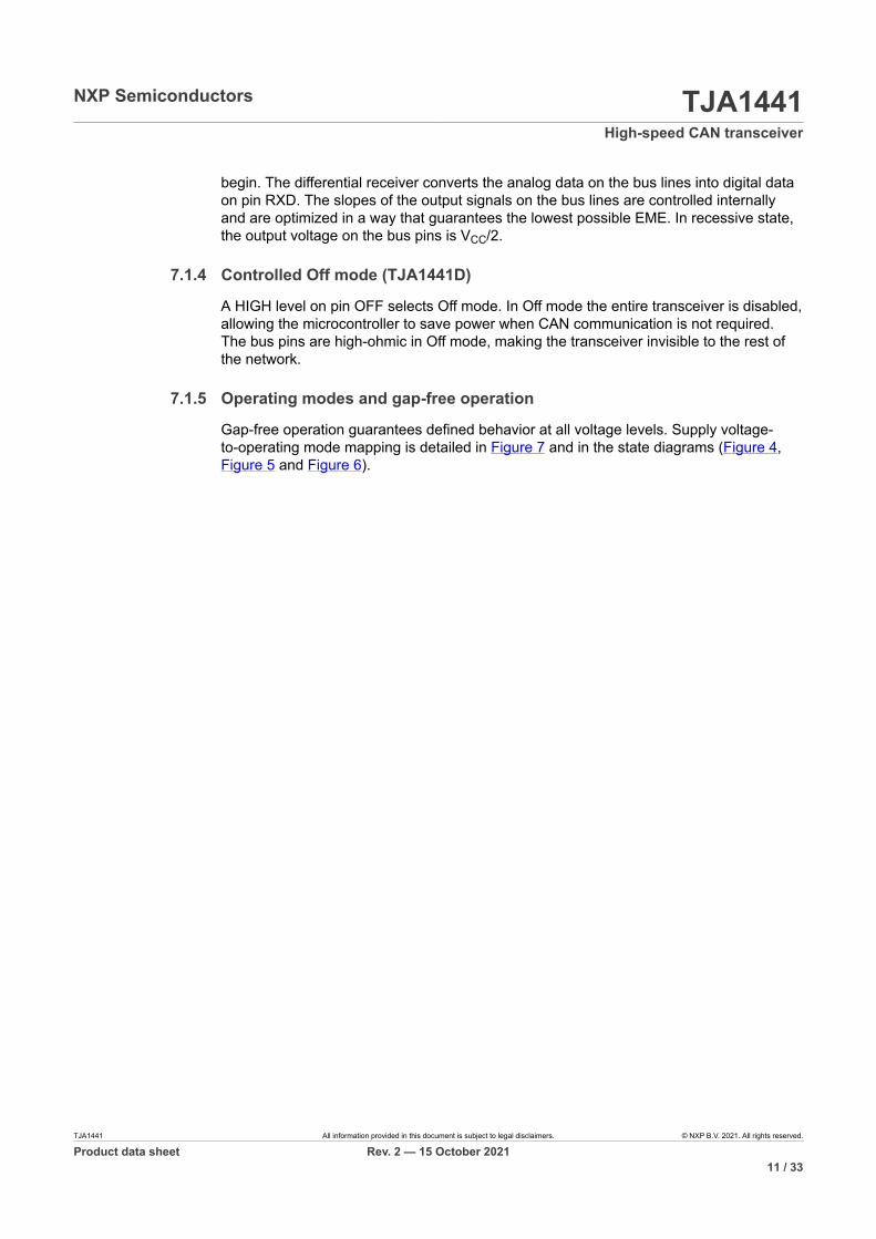
7.1 Operating modesThe TJA1441 supports three operating modes, Normal, Silent and Off. The operatingmode is selected via pin S in the TJA1441A/B and via pins S_N and OFF in theTJA1441D. See Table 5 and Table 6 for a description of the operating modes undernormal supply conditions. Mode changes are completed after transition time tt(moch).
Inputs OutputsMode
Pin S Pin TXD CAN driver Pin RXD
LOW dominant LOW
LOW when bus dominant
Normal LOW
HIGH recessive
HIGH when bus recessive
LOW when bus dominantSilent HIGH X biased to VCC/2
HIGH when bus recessive
Off[1] X X high-ohmic state high-ohmic state
Table 5. Operating modes: TJA1441A/B
[1] Off mode is only entered when the voltage on supply pin VCC or VIO (TJA1441A) is below any undervoltage detectionthreshold (see Figure 4 and Figure 5).
Inputs OutputsMode
Pin S_N Pin OFF Pin TXD CAN driver Pin RXD
LOW dominant LOW
LOW when bus dominant
Normal HIGH LOW
HIGH recessive
HIGH when bus recessive
LOW when bus dominantSilent LOW LOW X biased to VCC/2
HIGH when bus recessive
Off[1] X HIGH X high-ohmic state high-ohmic state
Table 6. Operating modes: TJA1441D
[1] Off mode is also entered when the voltage on supply pin VCC is below the undervoltage detection threshold (seeFigure 6).
TJA1441 All information provided in this document is subject to legal disclaimers. © NXP B.V. 2021. All rights reserved.
Product data sheet Rev. 2 — 15 October 20218 / 33
NXP Semiconductors TJA1441High-speed CAN transceiver
aaa-031270
OFF(CAN BIAS
= high-ohmic)
NORMAL(CAN BIAS= VCC/2)
SILENT(CAN BIAS= VCC/2)
S = HIGH ANDNOT(VCC < Vuvd(VCC) for t > tdet(uv))
VCC < Vuvd(VCC) for t > tdet(uv)
from any mode whenVIO < Vuvd(swoff)(VIO) for t > tuvd(swoff)
VCC < Vuvd(VCC) for t > tdet(uv)
S = LOW AND NOT(VCC < Vuvd(VCC) for t > tdet(uv))
S = LOWAND VCC > Vuvd(VCC) for t > trec(uv)
AND VIO > Vuvd(swoff)(VIO) for t > tstartup
S = HIGHAND VCC > Vuvd(VCC) for t > trec(uv)
AND VIO > Vuvd(swoff)(VIO) for t > tstartup
Figure 4. TJA1441A state diagram
aaa-036910
OFF(CAN BIAS
= high-ohmic)
NORMAL(CAN BIAS= VCC/2)
SILENT(CAN BIAS= VCC/2)
S = HIGH ANDNOT(VCC < Vuvd(VCC) for t > tdet(uv))
VCC < Vuvd(VCC) for t > tdet(uv)
VCC < Vuvd(VCC) for t > tdet(uv)
S = LOW AND NOT(VCC < Vuvd(VCC) for t > tdet(uv))
S = LOWAND VCC > Vuvd(VCC) for t > trec(uv)
AND VCC > Vuvd(swoff)(VCC) for t > tstartup
S = HIGHAND VCC > Vuvd(VCC) for t > trec(uv)
AND VCC > Vuvd(swoff)(VCC) for t > tstartup
from any mode whenVCC < Vuvd(swoff)(VCC) for t > tuvd(swoff)
Figure 5. TJA1441B state diagram
TJA1441 All information provided in this document is subject to legal disclaimers. © NXP B.V. 2021. All rights reserved.
Product data sheet Rev. 2 — 15 October 20219 / 33
NXP Semiconductors TJA1441High-speed CAN transceiver
aaa-036911
OFF(CAN BIAS
= high-ohmic)
NORMAL(CAN BIAS= VCC/2)
SILENT(CAN BIAS= VCC/2)
S_N = LOW AND OFF = LOW ANDNOT(VCC < Vuvd(VCC) for t > tdet(uv))
VCC < Vuvd(VCC) for t > tdet(uv)OR OFF = HIGH
VCC < Vuvd(VCC) for t > tdet(uv)OR OFF = HIGH
S_N = HIGH AND OFF = LOW AND NOT(VCC < Vuvd(VCC) for t > tdet(uv))
S_N = HIGH AND OFF = LOWAND VCC > Vuvd(VCC) for t > trec(uv)
AND VCC > Vuvd(swoff)(VCC) for t > tstartup
S_N = LOW AND OFF = LOWAND VCC > Vuvd(VCC) for t > trec(uv)
AND VCC > Vuvd(swoff)(VCC) for t > tstartup
from any mode whenVCC < Vuvd(swoff)(VCC) for t > tuvd(swoff)
Figure 6. TJA1441D state diagram
7.1.1 Off mode
The TJA1441 switches to Off mode from any mode when the supply voltage on pinVIO/VCC falls below the switch-off undervoltage detection threshold (Vuvd(swoff)(VIO) inTJA1441A; Vuvd(swoff)(VCC) in TJA1441B/D) or when VCC drops below Vuvd(VCC). This isthe default mode when the supply is first connected.
The CAN pins and pin RXD are in a high-ohmic state in Off mode.
When the supply voltage rises above the switch-off undervoltage detection threshold,the TJA1441 starts to boot up, triggering an initialization procedure. It switches to theselected mode after tstartup, provided VCC > Vuvd(VCC).
7.1.2 Silent mode
A HIGH level on pin S selects Silent mode in the TJA1441A and TJA1441B.
A LOW level on pins S_N and OFF selects Silent mode in the TJA1441D.
The transmitter is disabled in Silent mode, releasing the bus pins to VCC/2. All other ICfunctions, including the receiver, continue to operate as in Normal mode. Silent mode canbe used to prevent a faulty CAN controller disrupting network communications.
7.1.3 Normal mode
A LOW level on pin S selects Normal mode in the TJA1441A and TJA1441B.
A HIGH level on pin S_N and a LOW level on pin OFF selects Normal mode in theTJA1441D.
In Normal mode, the transceiver can transmit and receive data via bus lines CANH andCANL. Pin TXD must be HIGH at least once in Normal mode before transmission can
TJA1441 All information provided in this document is subject to legal disclaimers. © NXP B.V. 2021. All rights reserved.
Product data sheet Rev. 2 — 15 October 202110 / 33
NXP Semiconductors TJA1441High-speed CAN transceiver
begin. The differential receiver converts the analog data on the bus lines into digital dataon pin RXD. The slopes of the output signals on the bus lines are controlled internallyand are optimized in a way that guarantees the lowest possible EME. In recessive state,the output voltage on the bus pins is VCC/2.
7.1.4 Controlled Off mode (TJA1441D)
A HIGH level on pin OFF selects Off mode. In Off mode the entire transceiver is disabled,allowing the microcontroller to save power when CAN communication is not required.The bus pins are high-ohmic in Off mode, making the transceiver invisible to the rest ofthe network.
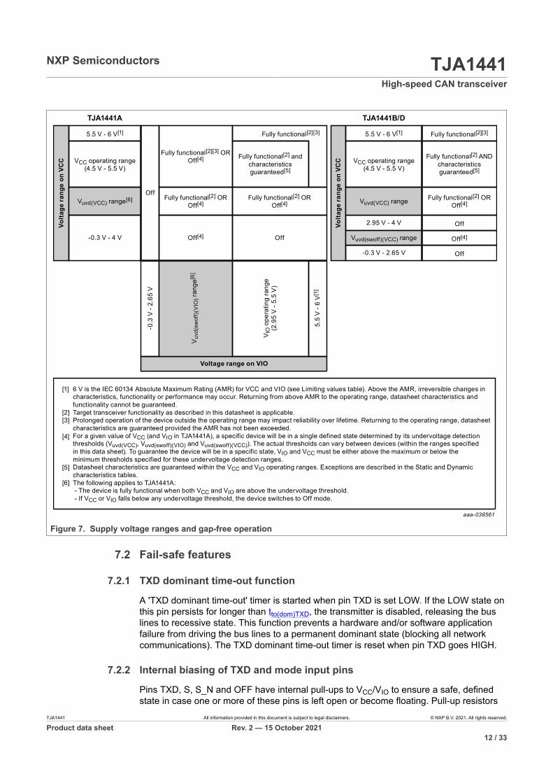
7.1.5 Operating modes and gap-free operation
Gap-free operation guarantees defined behavior at all voltage levels. Supply voltage-to-operating mode mapping is detailed in Figure 7 and in the state diagrams (Figure 4,Figure 5 and Figure 6).
TJA1441 All information provided in this document is subject to legal disclaimers. © NXP B.V. 2021. All rights reserved.
Product data sheet Rev. 2 — 15 October 202111 / 33
NXP Semiconductors TJA1441High-speed CAN transceiver
aaa-038561
6 V is the IEC 60134 Absolute Maximum Rating (AMR) for VCC and VIO (see Limiting values table). Above the AMR, irreversible changes incharacteristics, functionality or performance may occur. Returning from above AMR to the operating range, datasheet characteristics andfunctionality cannot be guaranteed.Target transceiver functionality as described in this datasheet is applicable.Prolonged operation of the device outside the operating range may impact reliability over lifetime. Returning to the operating range, datasheetcharacteristics are guaranteed provided the AMR has not been exceeded. For a given value of VCC (and VIO in TJA1441A), a specific device will be in a single defined state determined by its undervoltage detection thresholds (Vuvd(VCC), Vuvd(swoff)(VIO) and Vuvd(swoff)(VCC)). The actual thresholds can vary between devices (within the ranges specified in this data sheet). To guarantee the device will be in a specific state, VIO and VCC must be either above the maximum or below the minimum thresholds specified for these undervoltage detection ranges.Datasheet characteristics are guaranteed within the VCC and VIO operating ranges. Exceptions are described in the Static and Dynamiccharacteristics tables.The following applies to TJA1441A: - The device is fully functional when both VCC and VIO are above the undervoltage threshold. - If VCC or VIO falls below any undervoltage threshold, the device switches to Off mode.
Volta
ge ra
nge
on V
CC
Volta
ge ra
nge
on V
CC
Off
Fully functional[2][3] OROff[4]
Fully functional[2] OROff[4]
5.5 V - 6 V[1]
2.95 V - 4 V
-0.3
V -
2.65
V
V uvd
(sw
off)
(VIO
) ran
ge[6
]
V IO
ope
ratin
g ra
nge
(2.9
5 V
- 5.5
V)
5.5
V - 6
V[1
]
Vuvd(swoff)(VCC) range
-0.3 V - 2.65 V
Fully functional[2][3]
Off[4]
Fully functional[2] ANDcharacteristicsguaranteed[5]
Fully functional[2] OROff[4]
Off
Off[4]
Fully functional[2][3]
Off
Fully functional[2] andcharacteristicsguaranteed[5]
Fully functional[2] OROff[4]
Off
Vuvd(VCC) range[6]
-0.3 V - 4 V
VCC operating range(4.5 V - 5.5 V)
TJA1441A
Voltage range on VIO
5.5 V - 6 V[1]
Vuvd(VCC) range
VCC operating range(4.5 V - 5.5 V)
TJA1441B/D
[1]
[2][3]
[4]
[5]
[6]
Figure 7. Supply voltage ranges and gap-free operation
7.2 Fail-safe features
7.2.1 TXD dominant time-out function
A 'TXD dominant time-out' timer is started when pin TXD is set LOW. If the LOW state onthis pin persists for longer than tto(dom)TXD, the transmitter is disabled, releasing the buslines to recessive state. This function prevents a hardware and/or software applicationfailure from driving the bus lines to a permanent dominant state (blocking all networkcommunications). The TXD dominant time-out timer is reset when pin TXD goes HIGH.
7.2.2 Internal biasing of TXD and mode input pins
Pins TXD, S, S_N and OFF have internal pull-ups to VCC/VIO to ensure a safe, definedstate in case one or more of these pins is left open or become floating. Pull-up resistors
TJA1441 All information provided in this document is subject to legal disclaimers. © NXP B.V. 2021. All rights reserved.
Product data sheet Rev. 2 — 15 October 202112 / 33
NXP Semiconductors TJA1441High-speed CAN transceiver
are active on these pins in all states; they should be held at the VCC/VIO level in Silent (orOff in TJA1441D) mode to minimize supply current.
7.2.3 Undervoltage detection on pins VCC and VIO
If VCC or VIO drops below the undervoltage detection threshold (Vuvd(VCC) or Vuvd(swoff)VCCfor VCC; Vuvd(swoff)VIO for VIO) the transceiver switches to Off mode and disengages fromthe bus (zero load; bus pins high-ohmic) until the supply voltage has recovered. If Normalmode is selected, the output drivers are enabled once both VCC and VIO are again withintheir operating ranges and TXD has been reset to HIGH.
7.2.4 Overtemperature protection
The device is protected against overtemperature conditions. If the junction temperatureexceeds the shutdown junction temperature, Tj(sd), the CAN bus drivers are disabled.When the junction temperature drops below Tj(sd)rel, the CAN bus drivers recover onceTXD has been reset to HIGH and Normal mode is selected (waiting for TXD to go HIGHprevents output driver oscillation due to small variations in temperature).
7.2.5 I/O levels
Pin VIO of the TJA1441A should be connected to the microcontroller supply voltage (seeFigure 11). This adjusts the signal levels on pins TXD, RXD and S to the I/O levels of themicrocontroller, allowing for direct interfacing without additional glue logic.
All I/O levels are related to VCC in the TJA1441B/D and are, therefore, compatible with5 V microcontrollers. Spurious signals from the microcontroller on pins S, S_N and OFFare filtered out with a filter time of tfltr(IO).
TJA1441 All information provided in this document is subject to legal disclaimers. © NXP B.V. 2021. All rights reserved.
Product data sheet Rev. 2 — 15 October 202113 / 33
NXP Semiconductors TJA1441High-speed CAN transceiver
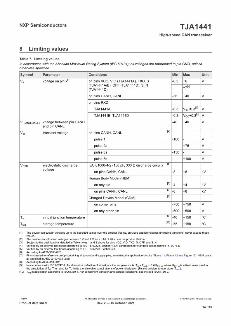
8 Limiting values
In accordance with the Absolute Maximum Rating System (IEC 60134); all voltages are referenced to pin GND, unlessotherwise specified.
Symbol Parameter Conditions Min Max Unit
-0.3 +6 Von pins VCC, VIO (TJA1441A), TXD, S(TJA1441A/B), OFF (TJA1441D), S_N(TJA1441D) - +7[2]
on pins CANH, CANL -36 +40 V
on pins RXD
TJA1441A -0.3 VIO+0.3[3] V
Vx voltage on pin x[1]
TJA1441B, TJA1441D -0.3 VCC+0.3[3] V
V(CANH-CANL) voltage between pin CANHand pin CANL
-40 +40 V
on pins CANH, CANL [4]
pulse 1 -100 - V
pulse 2a - +75 V
pulse 3a -150 - V
Vtrt transient voltage
pulse 3b - +100 V
IEC 61000-4-2 (150 pF, 330 Ω discharge circuit) [5]
on pins CANH, CANL -8 +8 kV
Human Body Model (HBM)
on any pin [6] -4 +4 kV
on pins CANH, CANL [7] -8 +8 kV
Charged Device Model (CDM) [8]
on corner pins -750 +750 V
VESD electrostatic dischargevoltage
on any other pin -500 +500 V
Tvj virtual junction temperature [9] -40 +150 °C
Tstg storage temperature [10] -55 +150 °C
Table 7. Limiting values
[1] The device can sustain voltages up to the specified values over the product lifetime, provided applied voltages (including transients) never exceed thesevalues.
[2] The device can withstand voltages between 6 V and 7 V for a total of 20 s over the product lifetime.[3] Subject to the qualifications detailed in Table notes 1 and 2 above for pins VCC, VIO, TXD, S, OFF, and S_N.[4] Verified by an external test house according to IEC TS 62228, Section 4.2.4; parameters for standard pulses defined in ISO7637.[5] Verified by an external test house according to IEC TS 62228, Section 4.3.[6] According to AEC-Q100-002.[7] Pins stressed to reference group containing all ground and supply pins, emulating the application circuits (Figure 11, Figure 12 and Figure 13). HBM pulse
as specified in AEC-Q100-002 used.[8] According to AEC-Q100-011.[9] In accordance with IEC 60747-1. An alternative definition of virtual junction temperature is: Tvj = Tamb + P # Rth(j-a), where Rth(j-a) is a fixed value used in
the calculation of Tvj. The rating for Tvj limits the allowable combinations of power dissipation (P) and ambient temperature (Tamb).[10] Tstg in application according to IEC61360-4. For component transport and storage conditions, see instead IEC61760-2.
TJA1441 All information provided in this document is subject to legal disclaimers. © NXP B.V. 2021. All rights reserved.
Product data sheet Rev. 2 — 15 October 202114 / 33
NXP Semiconductors TJA1441High-speed CAN transceiver
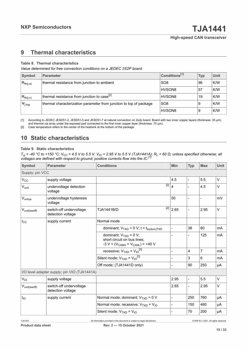
9 Thermal characteristics
Value determined for free convection conditions on a JEDEC 2S2P board.
Symbol Parameter Conditions[1] Typ Unit
SO8 96 K/WRth(j-a) thermal resistance from junction to ambient
HVSON8 57 K/W
Rth(j-c) thermal resistance from junction to case[2] HVSON8 19 K/W
SO8 9 K/WѰj-top thermal characterization parameter from junction to top of package
HVSON8 9 K/W
Table 8. Thermal characteristics
[1] According to JEDEC JESD51-2, JESD51-5 and JESD51-7 at natural convection on 2s2p board. Board with two inner copper layers (thickness: 35 μm)and thermal via array under the exposed pad connected to the first inner copper layer (thickness: 70 μm).
[2] Case temperature refers to the center of the heatsink at the bottom of the package.
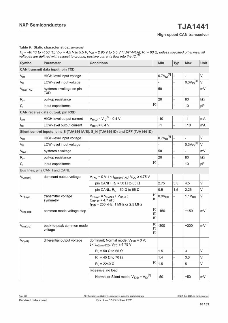
10 Static characteristics
Tvj = -40 °C to +150 °C; VCC = 4.5 V to 5.5 V; VIO = 2.95 V to 5.5 V (TJA1441A); RL = 60 Ω; unless specified otherwise; allvoltages are defined with respect to ground; positive currents flow into the IC.[1]
Symbol Parameter Conditions Min Typ Max Unit
Supply; pin VCC
VCC supply voltage 4.5 - 5.5 V
Vuvd undervoltage detectionvoltage
[2] 4 - 4.5 V
Vuvhys undervoltage hysteresisvoltage
50 - - mV
Vuvd(swoff) switch-off undervoltagedetection voltage
TJA1441B/D [2] 2.65 - 2.95 V
Normal mode
dominant; VTXD = 0 V; t < tto(dom)TXD - 38 60 mA
dominant; VTXD = 0 V;short circuit on bus lines;-3 V < (VCANH = VCANL) < +40 V
- - 125 mA
recessive; VTXD = VIO[3] - 4 7 mA
Silent mode; VTXD = VIO[3] - 3 6 mA
ICC supply current
Off mode; (TJA1441D only) - 90 250 μA
I/O level adapter supply; pin VIO (TJA1441A)
VIO supply voltage 2.95 - 5.5 V
Vuvd(swoff) switch-off undervoltagedetection voltage
2.65 - 2.95 V
Normal mode; dominant; VTXD = 0 V - 250 760 µA
Normal mode; recessive; VTXD = VIO - 150 460 µA
IIO supply current
Silent mode; VTXD = VIO - 70 200 µA
Table 9. Static characteristics
TJA1441 All information provided in this document is subject to legal disclaimers. © NXP B.V. 2021. All rights reserved.
Product data sheet Rev. 2 — 15 October 202115 / 33
NXP Semiconductors TJA1441High-speed CAN transceiver
Tvj = -40 °C to +150 °C; VCC = 4.5 V to 5.5 V; VIO = 2.95 V to 5.5 V (TJA1441A); RL = 60 Ω; unless specified otherwise; allvoltages are defined with respect to ground; positive currents flow into the IC.[1]
Symbol Parameter Conditions Min Typ Max Unit
CAN transmit data input; pin TXD
VIH HIGH-level input voltage 0.7VIO[3] - - V
VIL LOW-level input voltage - - 0.3VIO[3] V
Vhys(TXD) hysteresis voltage on pinTXD
50 - - mV
Rpu pull-up resistance 20 - 80 kΩ
Ci input capacitance [4] - - 10 pF
CAN receive data output; pin RXD
IOH HIGH-level output current VRXD = VIO[3] - 0.4 V -10 - -1 mA
IOL LOW-level output current VRXD = 0.4 V +1 - +10 mA
Silent control inputs; pins S (TJA1441A/B), S_N (TJA1441D) and OFF (TJA1441D)
VIH HIGH-level input voltage 0.7VIO[3] - - V
VIL LOW-level input voltage - - 0.3VIO[3] V
Vhys hysteresis voltage 50 - - mV
Rpu pull-up resistance 20 - 80 kΩ
Ci input capacitance [4] - - 10 pF
Bus lines; pins CANH and CANL
VTXD = 0 V; t < tto(dom)TXD; VCC ≥ 4.75 V
pin CANH; RL = 50 Ω to 65 Ω 2.75 3.5 4.5 V
VO(dom) dominant output voltage
pin CANL; RL = 50 Ω to 65 Ω 0.5 1.5 2.25 V
VTXsym transmitter voltagesymmetry
VTXsym = VCANH + VCANL;CSPLIT = 4.7 nF;fTXD = 250 kHz, 1 MHz or 2.5 MHz
[4][5]
0.9VCC - 1.1VCC V
Vcm(step) common mode voltage step [4][5][6]
-150 - +150 mV
Vcm(p-p) peak-to-peak common modevoltage
[4][5][6]
-300 - +300 mV
dominant; Normal mode; VTXD = 0 V;t < tto(dom)TXD; VCC ≥ 4.75 V
RL = 50 Ω to 65 Ω 1.5 - 3 V
RL = 45 Ω to 70 Ω 1.4 - 3.3 V
RL = 2240 Ω [4] 1.5 - 5 V
recessive; no load
VO(dif) differential output voltage
Normal or Silent mode; VTXD = VIO[3] -50 - +50 mV
Table 9. Static characteristics...continued
TJA1441 All information provided in this document is subject to legal disclaimers. © NXP B.V. 2021. All rights reserved.
Product data sheet Rev. 2 — 15 October 202116 / 33
NXP Semiconductors TJA1441High-speed CAN transceiver
Tvj = -40 °C to +150 °C; VCC = 4.5 V to 5.5 V; VIO = 2.95 V to 5.5 V (TJA1441A); RL = 60 Ω; unless specified otherwise; allvoltages are defined with respect to ground; positive currents flow into the IC.[1]
Symbol Parameter Conditions Min Typ Max Unit
VO(rec) recessive output voltage Normal or Silent mode; VTXD = VIO[3]; no
load2 2.5 3 V
Vth(RX)dif differential receiverthreshold voltage
Normal or Silent mode;-12 V ≤ VCANH ≤ +12 V;-12 V ≤ VCANL ≤ +12 V
0.5 - 0.9 V
Vrec(RX) receiver recessive voltage Normal or Silent mode;-12 V ≤ VCANH ≤ +12 V;-12 V ≤ VCANL ≤ +12 V
-4 - 0.5 V
Vdom(RX) receiver dominant voltage Normal or Silent mode;-12 V ≤ VCANH ≤ +12 V;-12 V ≤ VCANL ≤ +12 V
0.9 - 9 V
Vhys(RX)dif differential receiverhysteresis voltage
Normal or Silent mode;-12 V ≤ VCANH ≤ +12 V;-12 V ≤ VCANL ≤ +12 V
50 - - mV
IO(sc) short-circuit output current -15 V ≤ VCANH ≤ +40 V;-15 V ≤ VCANL ≤ +40 V
- - 115 mA
IO(sc)rec recessive short-circuit outputcurrent
Normal mode; VTXD = VIO[3];
-27 V ≤ VCANH ≤ +32 V;-27 V ≤ VCANL ≤ +32 V
-3 - +3 mA
IL leakage current VCC = VIO = 0 V or pins shorted to GNDvia 47 KΩ; VCANH = VCANL = 5 V;
-10 - +10 µA
Ri input resistance -2 V ≤ VCANL ≤ +7 V;-2 V ≤ VCANH ≤ +7 V
25 40 50 kΩ
ΔRi input resistance deviation 0 V ≤ VCANL ≤ +5 V; 0 V ≤ VCANH ≤ +5 V -3 - +3 %
Ri(dif) differential input resistance -2 V ≤ VCANL ≤ +7 V;-2 V ≤ VCANH ≤ +7 V
50 80 100 kΩ
Ci(cm) common-mode inputcapacitance
[4] - - 20 pF
Ci(dif) differential input capacitance [4] - - 10 pF
Temperature detection
Tj(sd) shutdown junctiontemperature
180 - 200 °C
Tj(sd)rel release shutdown junctiontemperature
175 - 195 °C
Table 9. Static characteristics...continued
[1] All parameters are guaranteed over the virtual junction temperature range by design. Factory testing uses correlated test conditions to cover the specifiedtemperature and power supply voltage range.
[2] Undervoltage is detected between min and max values. Undervoltage is guaranteed to be detected below min value and guaranteed not to be detectedabove max value.
[3] VCC in TJA1441B/D[4] Not tested in production; guaranteed by design.[5] The test circuit used to measure the bus output voltage symmetry (which includes CSPLIT) is shown in Figure 15[6] See Figure 10
TJA1441 All information provided in this document is subject to legal disclaimers. © NXP B.V. 2021. All rights reserved.
Product data sheet Rev. 2 — 15 October 202117 / 33
NXP Semiconductors TJA1441High-speed CAN transceiver
11 Dynamic characteristics
Tvj = −40 °C to +150 °C; VCC = 4.5 V to 5.5 V; VIO = 2.95 V to 5.5 V (TJA1441A); RL = 60 Ω; unless specified otherwise. Allvoltages are defined with respect to ground.[1]
Symbol Parameter Conditions Min Typ Max Unit
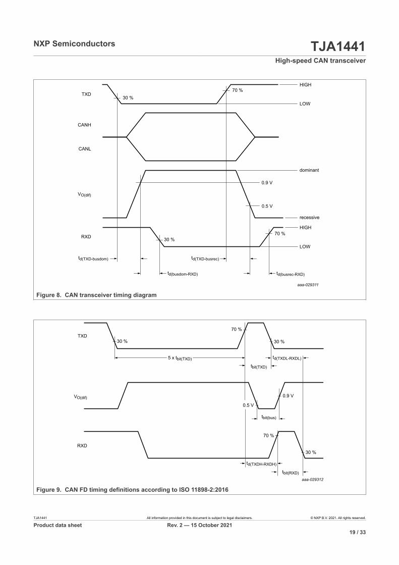
CAN timing characteristics; tbit(TXD) ≥ 200 ns; see Figure 8, Figure 9 and Figure 14
td(TXD-busdom) delay time from TXD to bus dominant Normal mode - - 102.5 ns
td(TXD-busrec) delay time from TXD to bus recessive Normal mode - - 102.5 ns
td(busdom-RXD) delay time from bus dominant to RXD Normal or Silent mode - - 115 ns
td(busrec-RXD) delay time from bus recessive to RXD Normal or Silent mode - - 115 ns
td(TXDL-RXDL) delay time from TXD LOW to RXD LOW Normal mode - - 215 ns
td(TXDH-RXDH) delay time from TXD HIGH to RXD HIGH Normal mode - - 215 ns
CAN FD timing characteristics; see Figure 9 and Figure 14
tbit(TXD) = 500 ns 435 - 530 nstbit(bus) transmitted recessive bit width
tbit(TXD) = 200 ns 155 - 210 ns
tbit(TXD) = 500 ns 400 - 550 nstbit(RXD) bit time on pin RXD
tbit(TXD) = 200 ns 120 - 220 ns
tbit(TXD) = 500 ns -65 - 40 nsΔtrec receiver timing symmetry
tbit(TXD) = 200 ns -45 - 15 ns
Dominant time-out time; pin TXD
tto(dom)TXD TXD dominant time-out time VTXD = 0 V; Normal mode [2][3]
0.8 - 9 ms
Mode transitions
tt(moch) mode change transition time [2] - - 50 µs
tstartup start-up time [2] - - 1 ms
IO filter; pins S (TJA1441A/B), S_N (TJA1441D) and OFF (TJA1441D)
tfltr(IO) I/O filter time [4] 1 - 5 µs
Undervoltage detection; see Figure 4, Figure 5 and Figure 6
tdet(uv) undervoltage detection time on pin VCC [2] - - 30 µs
on pin VCC; TJA1441B/D [2] - - 30 µstuvd(swoff) switch-off undervoltage detection time
on pin VIO; TJA1441A [2] - - 30 µs
trec(uv) undervoltage recovery time on pin VCC [2] - - 50 µs
Table 10. Dynamic characteristics
[1] All parameters are guaranteed over the junction temperature range by design. Factory testing uses correlated test conditions to cover the specifiedtemperature and power supply voltage ranges.
[2] Not tested in production; guaranteed by design.[3] Time-out occurs between the min and max values. Time-out is guaranteed not to occur below the min value; time-out is guaranteed to occur above the
max value.[4] Pulses shorter than the min value are guaranteed to be filtered out; pulses longer than the max value are guaranteed to be processed.
TJA1441 All information provided in this document is subject to legal disclaimers. © NXP B.V. 2021. All rights reserved.
Product data sheet Rev. 2 — 15 October 202118 / 33
NXP Semiconductors TJA1441High-speed CAN transceiver
aaa-029311
CANH
CANL
td(TXD-busdom)
TXD
VO(dif)
RXD
HIGH
HIGH
LOW
LOW
dominant
recessive
td(busdom-RXD)
td(TXD-busrec)
td(busrec-RXD)
0.9 V
0.5 V
30 %
30 %
70 %
70 %
Figure 8. CAN transceiver timing diagram
tbit(TXD)
5 x tbit(TXD)
70 %
30 %30 %TXD
tbit(bus)
0.9 VVO(dif)
aaa-029312
tbit(RXD)
70 %
30 %RXD
td(TXDL-RXDL)
td(TXDH-RXDH)
0.5 V
Figure 9. CAN FD timing definitions according to ISO 11898-2:2016
TJA1441 All information provided in this document is subject to legal disclaimers. © NXP B.V. 2021. All rights reserved.
Product data sheet Rev. 2 — 15 October 202119 / 33
NXP Semiconductors TJA1441High-speed CAN transceiver
aaa-037830
CANH
CANL
VCANH + VCANL
Vcm(step)
Vcm(p-p)
Figure 10. CAN bus common-mode voltage
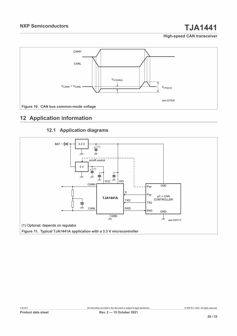
12 Application information
12.1 Application diagrams
aaa-030773
VDD
Pyy
TX0TXD
CANH
TJA1441A
CANL
VIO
3.3 VBAT
5 V
RXD
S
GNDGND
µC + CANCONTROLLER
RX0
(1)
VCC
(1)
Pxx
on/off control
(1) Optional, depends on regulator.Figure 11. Typical TJA1441A application with a 3.3 V microcontroller
TJA1441 All information provided in this document is subject to legal disclaimers. © NXP B.V. 2021. All rights reserved.
Product data sheet Rev. 2 — 15 October 202120 / 33
NXP Semiconductors TJA1441High-speed CAN transceiver
TJA1441B
S
TXD
RXD
CONTROLLER
Pxx
TX0
RX0
VDD
GNDGND
VCC
CANH
CANL
5 VBAT
aaa-030772
(1)
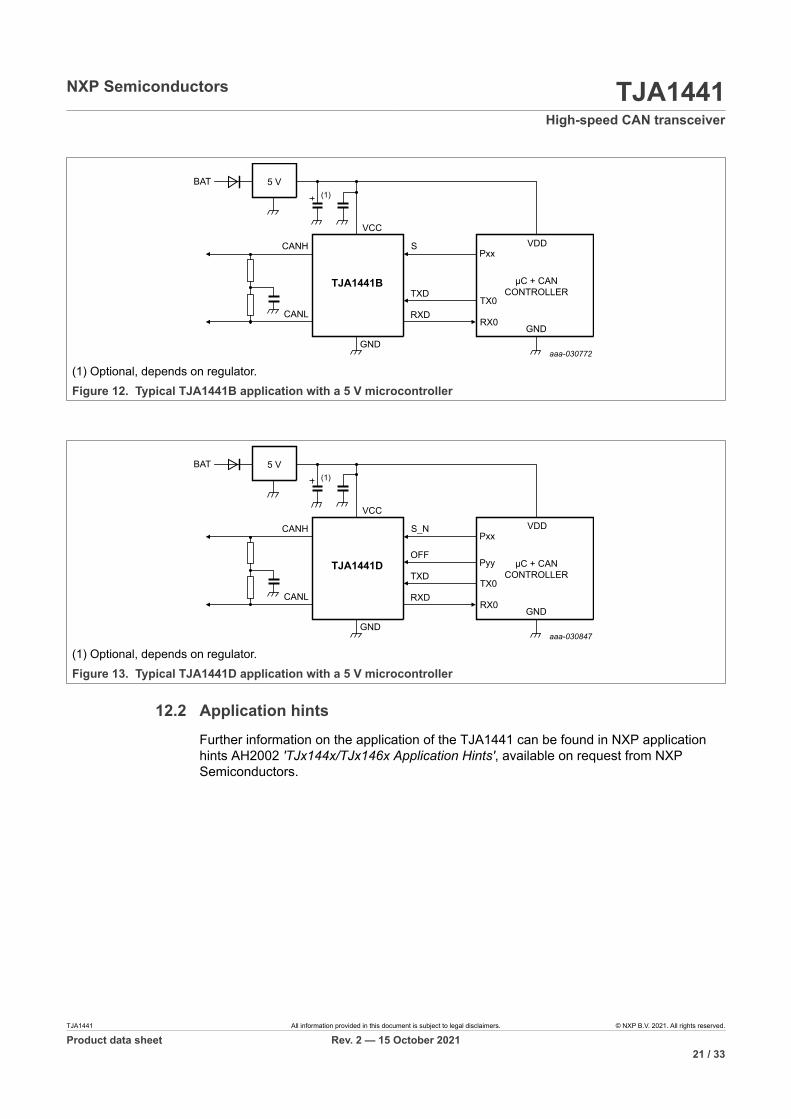
(1) Optional, depends on regulator.Figure 12. Typical TJA1441B application with a 5 V microcontroller
TJA1441D
S_N
TXD
RXD
CONTROLLER
Pxx
TX0
RX0
VDD
GNDGND
VCC
CANH
CANL
5 VBAT
aaa-030847
(1)
OFFPyy
(1) Optional, depends on regulator.Figure 13. Typical TJA1441D application with a 5 V microcontroller
12.2 Application hintsFurther information on the application of the TJA1441 can be found in NXP applicationhints AH2002 'TJx144x/TJx146x Application Hints', available on request from NXPSemiconductors.
TJA1441 All information provided in this document is subject to legal disclaimers. © NXP B.V. 2021. All rights reserved.
Product data sheet Rev. 2 — 15 October 202121 / 33
NXP Semiconductors TJA1441High-speed CAN transceiver
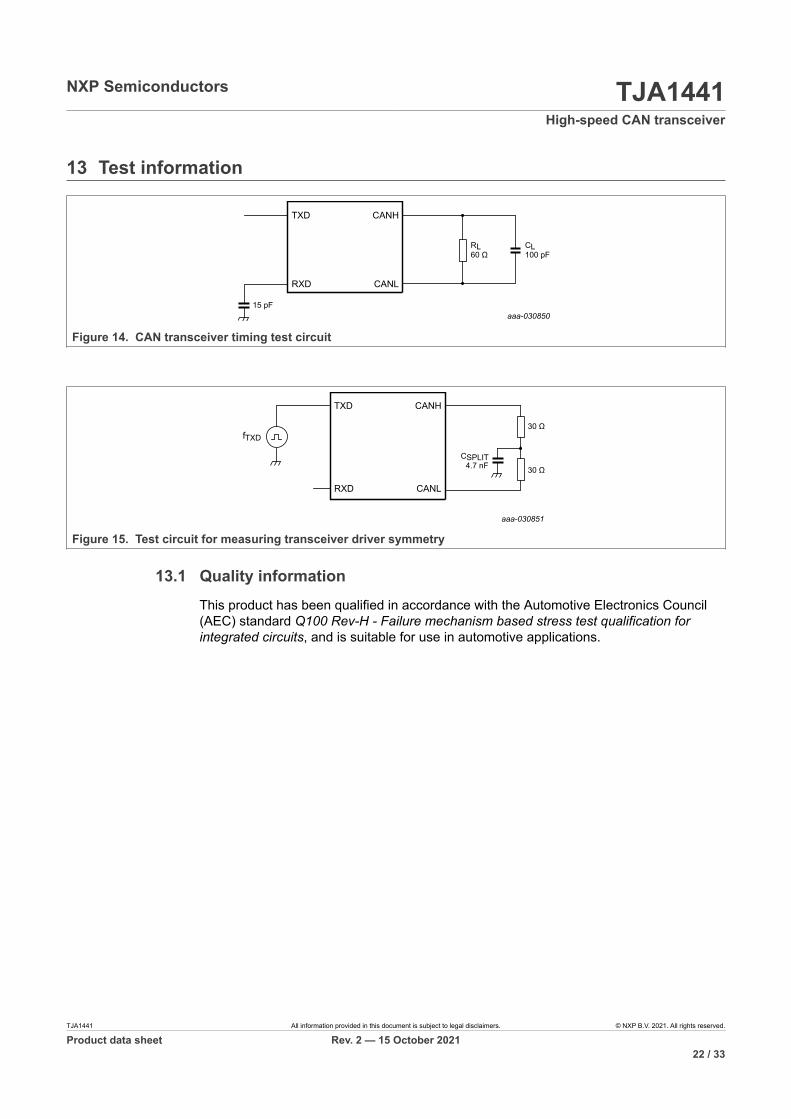
13 Test information
aaa-030850
TXD
RXD
15 pF
CANL
CANH
RL60 Ω
CL100 pF
Figure 14. CAN transceiver timing test circuit
aaa-030851
30 Ω
30 Ω
CSPLIT4.7 nF
TXD
RXD CANL
CANH
fTXD
Figure 15. Test circuit for measuring transceiver driver symmetry
13.1 Quality informationThis product has been qualified in accordance with the Automotive Electronics Council(AEC) standard Q100 Rev-H - Failure mechanism based stress test qualification forintegrated circuits, and is suitable for use in automotive applications.
TJA1441 All information provided in this document is subject to legal disclaimers. © NXP B.V. 2021. All rights reserved.
Product data sheet Rev. 2 — 15 October 202122 / 33
NXP Semiconductors TJA1441High-speed CAN transceiver
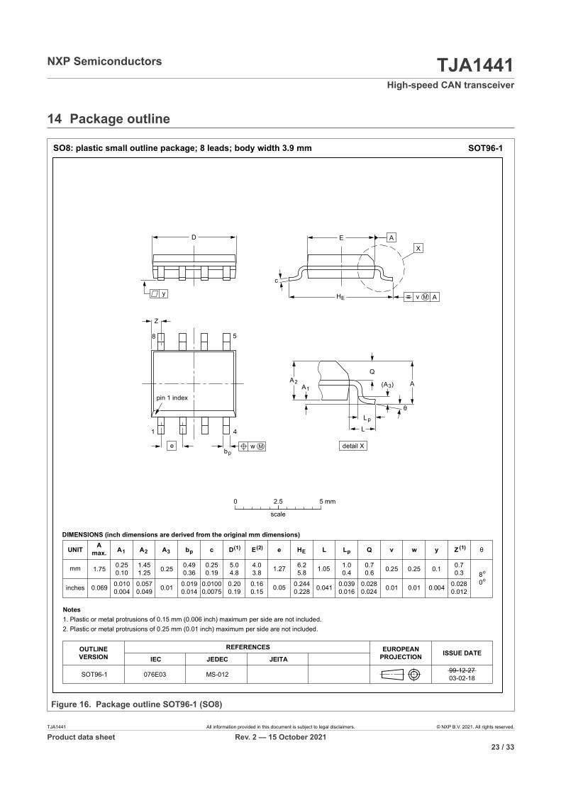
14 Package outline
UNIT A max. A 1 A 2 A 3 b p c D (1) E (2) (1) e H E L L p Q Z y w v θ
REFERENCES OUTLINE VERSION
EUROPEAN PROJECTION ISSUE DATE
IEC JEDEC JEITA
mm
inches
1.75 0.25 0.10
1.45 1.25 0.25 0.49
0.36 0.25 0.19
5.0 4.8
4.0 3.8 1.27 6.2
5.8 1.05 0.7 0.6
0.7 0.3 8
0
o o
0.25 0.1 0.25
DIMENSIONS (inch dimensions are derived from the original mm dimensions)
Notes 1. Plastic or metal protrusions of 0.15 mm (0.006 inch) maximum per side are not included. 2. Plastic or metal protrusions of 0.25 mm (0.01 inch) maximum per side are not included.
1.0 0.4
SOT96-1
X
w M
θ
A A 1 A 2
b p
D
H E
L p
Q
detail X
E
Z
e
c
L
v M A
(A ) 3
A
4
5
pin 1 index
1
8
y
076E03 MS-012
0.069 0.010 0.004
0.057 0.049 0.01 0.019
0.014 0.0100 0.0075
0.20 0.19
0.16 0.15 0.05 0.244
0.228 0.028 0.024
0.028 0.012 0.01 0.01 0.041 0.004 0.039
0.016
0 2.5 5 mm
scale
SO8: plastic small outline package; 8 leads; body width 3.9 mm SOT96-1
99-12-27 03-02-18
Figure 16. Package outline SOT96-1 (SO8)
TJA1441 All information provided in this document is subject to legal disclaimers. © NXP B.V. 2021. All rights reserved.
Product data sheet Rev. 2 — 15 October 202123 / 33
NXP Semiconductors TJA1441High-speed CAN transceiver
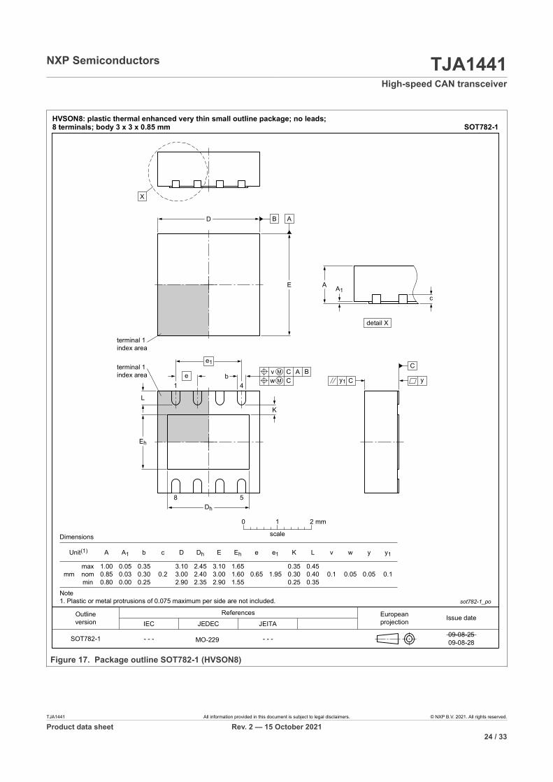
ReferencesOutline version
European projection Issue date
IEC JEDEC JEITA
SOT782-1 - - - - - -
sot782-1_po
09-08-25 09-08-28
Unit(1)
mmmax nom min
1.00 0.85 0.80
0.05 0.03 0.00
0.23.10 3.00 2.90
2.45 2.40 2.35
3.10 3.00 2.90
0.65 1.950.45 0.40 0.35
0.1
A
Dimensions
Note 1. Plastic or metal protrusions of 0.075 maximum per side are not included.
HVSON8: plastic thermal enhanced very thin small outline package; no leads; 8 terminals; body 3 x 3 x 0.85 mm SOT782-1
A1 b
0.35 0.30 0.25
c D Dh E Eh
1.65 1.60 1.55
e e1 K
0.35 0.30 0.25
L v
0.1
w
0.05
y
0.05
y1
0 1 2 mm
scale
MO-229
X
C
yCy1
detail X
A
cA1
B AD
E
terminal 1 index area
b
Dh
L
Eh
K
e1
e AC BvCw
1 4
8 5
terminal 1 index area
Figure 17. Package outline SOT782-1 (HVSON8)
TJA1441 All information provided in this document is subject to legal disclaimers. © NXP B.V. 2021. All rights reserved.
Product data sheet Rev. 2 — 15 October 202124 / 33
NXP Semiconductors TJA1441High-speed CAN transceiver
15 Handling information
All input and output pins are protected against ElectroStatic Discharge (ESD) undernormal handling. When handling ensure that the appropriate precautions are taken asdescribed in JESD625-A or equivalent standards.
16 Soldering of SMD packages
This text provides a very brief insight into a complex technology. A more in-depth accountof soldering ICs can be found in Application Note AN10365 “Surface mount reflowsoldering description”.
16.1 Introduction to solderingSoldering is one of the most common methods through which packages are attachedto Printed Circuit Boards (PCBs), to form electrical circuits. The soldered joint providesboth the mechanical and the electrical connection. There is no single soldering methodthat is ideal for all IC packages. Wave soldering is often preferred when through-holeand Surface Mount Devices (SMDs) are mixed on one printed wiring board; however, it isnot suitable for fine pitch SMDs. Reflow soldering is ideal for the small pitches and highdensities that come with increased miniaturization.
16.2 Wave and reflow solderingWave soldering is a joining technology in which the joints are made by solder comingfrom a standing wave of liquid solder. The wave soldering process is suitable for thefollowing:
• Through-hole components• Leaded or leadless SMDs, which are glued to the surface of the printed circuit board
Not all SMDs can be wave soldered. Packages with solder balls, and some leadlesspackages which have solder lands underneath the body, cannot be wave soldered. Also,leaded SMDs with leads having a pitch smaller than ~0.6 mm cannot be wave soldered,due to an increased probability of bridging.
The reflow soldering process involves applying solder paste to a board, followed bycomponent placement and exposure to a temperature profile. Leaded packages,packages with solder balls, and leadless packages are all reflow solderable.
Key characteristics in both wave and reflow soldering are:
• Board specifications, including the board finish, solder masks and vias• Package footprints, including solder thieves and orientation• The moisture sensitivity level of the packages• Package placement• Inspection and repair• Lead-free soldering versus SnPb soldering
16.3 Wave solderingKey characteristics in wave soldering are:
TJA1441 All information provided in this document is subject to legal disclaimers. © NXP B.V. 2021. All rights reserved.
Product data sheet Rev. 2 — 15 October 202125 / 33
NXP Semiconductors TJA1441High-speed CAN transceiver
• Process issues, such as application of adhesive and flux, clinching of leads, boardtransport, the solder wave parameters, and the time during which components areexposed to the wave
• Solder bath specifications, including temperature and impurities
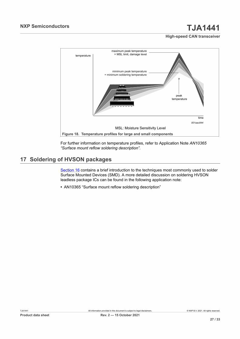
16.4 Reflow solderingKey characteristics in reflow soldering are:
• Lead-free versus SnPb soldering; note that a lead-free reflow process usually leadsto higher minimum peak temperatures (see Figure 18) than a SnPb process, thusreducing the process window
• Solder paste printing issues including smearing, release, and adjusting the processwindow for a mix of large and small components on one board
• Reflow temperature profile; this profile includes preheat, reflow (in which the boardis heated to the peak temperature) and cooling down. It is imperative that the peaktemperature is high enough for the solder to make reliable solder joints (a solderpaste characteristic). In addition, the peak temperature must be low enough that thepackages and/or boards are not damaged. The peak temperature of the packagedepends on package thickness and volume and is classified in accordance withTable 11 and Table 12
Package reflow temperature (°C)
Volume (mm³)
Package thickness (mm)
< 350 ≥ 350
< 2.5 235 220
≥ 2.5 220 220
Table 11. SnPb eutectic process (from J-STD-020D)
Package reflow temperature (°C)
Volume (mm³)
Package thickness (mm)
< 350 350 to 2000 > 2000
< 1.6 260 260 260
1.6 to 2.5 260 250 245
> 2.5 250 245 245
Table 12. Lead-free process (from J-STD-020D)
Moisture sensitivity precautions, as indicated on the packing, must be respected at alltimes.
Studies have shown that small packages reach higher temperatures during reflowsoldering, see Figure 18.
TJA1441 All information provided in this document is subject to legal disclaimers. © NXP B.V. 2021. All rights reserved.
Product data sheet Rev. 2 — 15 October 202126 / 33
NXP Semiconductors TJA1441High-speed CAN transceiver
001aac844
temperature
time
minimum peak temperature= minimum soldering temperature
maximum peak temperature= MSL limit, damage level
peak temperature
MSL: Moisture Sensitivity LevelFigure 18. Temperature profiles for large and small components
For further information on temperature profiles, refer to Application Note AN10365“Surface mount reflow soldering description”.
17 Soldering of HVSON packages
Section 16 contains a brief introduction to the techniques most commonly used to solderSurface Mounted Devices (SMD). A more detailed discussion on soldering HVSONleadless package ICs can be found in the following application note:
• AN10365 “Surface mount reflow soldering description”
TJA1441 All information provided in this document is subject to legal disclaimers. © NXP B.V. 2021. All rights reserved.
Product data sheet Rev. 2 — 15 October 202127 / 33
NXP Semiconductors TJA1441High-speed CAN transceiver
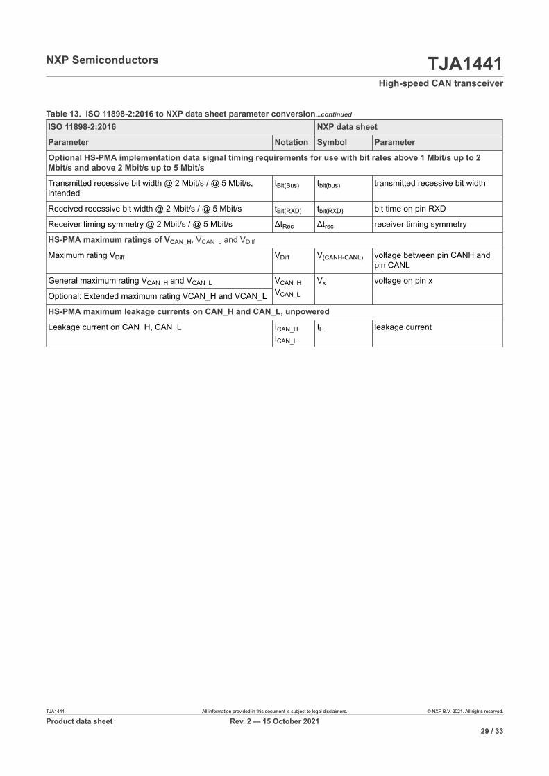
18 Appendix: ISO 11898-2:2016 parameter cross-reference list
ISO 11898-2:2016 NXP data sheet
Parameter Notation Symbol Parameter
HS-PMA dominant output characteristics
Single ended voltage on CAN_H VCAN_H
Single ended voltage on CAN_L VCAN_L
VO(dom) dominant output voltage
Differential voltage on normal bus load
Differential voltage on effective resistance during arbitration
Optional: Differential voltage on extended bus load range
VDiff VO(dif) differential output voltage
HS-PMA driver symmetry
Driver symmetry VSYM VTXsym transmitter voltage symmetry
Maximum HS-PMA driver output current
Absolute current on CAN_H ICAN_H
Absolute current on CAN_L ICAN_L
IO(sc)dom dominant short-circuit outputcurrent
HS-PMA recessive output characteristics, bus biasing active/inactive
Single ended output voltage on CAN_H VCAN_H
Single ended output voltage on CAN_L VCAN_L
VO(rec) recessive output voltage
Differential output voltage VDiff VO(dif) differential output voltage
Optional HS-PMA transmit dominant time-out
Transmit dominant time-out, long
Transmit dominant time-out, short
tdom tto(dom)TXD TXD dominant time-out time
HS-PMA static receiver input characteristics, bus biasing active/inactive
Vth(RX)dif differential receiver thresholdvoltage
Vrec(RX) receiver recessive voltage
Recessive state differential input voltage rangeDominant state differential input voltage range
VDiff
Vdom(RX) receiver dominant voltage
HS-PMA receiver input resistance (matching)
Differential internal resistance RDiff Ri(dif) differential input resistance
Single ended internal resistance RCAN_HRCAN_L
Ri input resistance
Matching of internal resistance MR ΔRi input resistance deviation
HS-PMA implementation loop delay requirement
td(TXDH-RXDH) delay time from TXD HIGH toRXD HIGH
Loop delay tLoop
td(TXDL-RXDL) delay time from TXD LOW toRXD LOW
Table 13. ISO 11898-2:2016 to NXP data sheet parameter conversion
TJA1441 All information provided in this document is subject to legal disclaimers. © NXP B.V. 2021. All rights reserved.
Product data sheet Rev. 2 — 15 October 202128 / 33
NXP Semiconductors TJA1441High-speed CAN transceiver
ISO 11898-2:2016 NXP data sheet
Parameter Notation Symbol Parameter
Optional HS-PMA implementation data signal timing requirements for use with bit rates above 1 Mbit/s up to 2Mbit/s and above 2 Mbit/s up to 5 Mbit/s
Transmitted recessive bit width @ 2 Mbit/s / @ 5 Mbit/s,intended
tBit(Bus) tbit(bus) transmitted recessive bit width
Received recessive bit width @ 2 Mbit/s / @ 5 Mbit/s tBit(RXD) tbit(RXD) bit time on pin RXD
Receiver timing symmetry @ 2 Mbit/s / @ 5 Mbit/s ΔtRec Δtrec receiver timing symmetry
HS-PMA maximum ratings of VCAN_H, VCAN_L and VDiff
Maximum rating VDiff VDiff V(CANH-CANL) voltage between pin CANH andpin CANL
General maximum rating VCAN_H and VCAN_L
Optional: Extended maximum rating VCAN_H and VCAN_L
VCAN_HVCAN_L
Vx voltage on pin x
HS-PMA maximum leakage currents on CAN_H and CAN_L, unpowered
Leakage current on CAN_H, CAN_L ICAN_HICAN_L
IL leakage current
Table 13. ISO 11898-2:2016 to NXP data sheet parameter conversion...continued
TJA1441 All information provided in this document is subject to legal disclaimers. © NXP B.V. 2021. All rights reserved.
Product data sheet Rev. 2 — 15 October 202129 / 33
NXP Semiconductors TJA1441High-speed CAN transceiver
19 Appendix: TJx144x/TJx146x/TJF1441 family overview
Modes Supplies Data rate Additional features
Device[1]
Nor
mal
Stan
dby
Slee
p
Sile
nt/L
iste
n-on
ly
Sele
ctab
le O
ff
VCC
pin
VIO
pin
VBAT
pin
Up
to 5
Mbi
t/s C
AN
FD
Up
to 8
Mbi
t/s C
AN
FD
[2]
Sign
al im
prov
emen
t[3]
Wak
e-up
sou
rce
reco
gniti
on[4
]
Shor
t WU
P su
ppor
t [0.
5 - 1
.8 µ
s][5
]
Sing
le s
uppl
y pi
n w
ake-
up[6
]
TXD
dom
inan
t tim
eout
Loca
l dia
gnos
tics
via
ERR
_N p
in
TJx1441A
TJx1441B
TJx1441D
TJF1441A [7]
TJx1442A
TJx1442B
TJx1443A
TJx1448A
TJx1448B
TJx1448C
TJx1462A
TJx1462B
TJx1463A
Table 14. Feature overview of the complete TJx144x/TJx146x/TJF1441 family
[1] TJx: TJA14xxx is AEC-Q100 Grade 1; TJR14xxx is AEC-Q100 Grade 0; TJF1441A is non-automotive grade.[2] Only guaranteed for TJA146x, AEC-Q100 Grade 1.[3] CAN FD Signal Improvement Capability (SIC) according to CiA 601-4:2019.[4] RXD is held LOW after wake-up request, enabling wake-up source recognition.[5] WUP = wake-up pattern according ISO11898-2:2016.[6] Only VIO supply needed for wake-up in TJA1442A, TJA1448A, TJA1448C, TJA1462A; only VBAT supply needed for wake-up in TJA1443A, TJA1463A.[7] Not having TXD dominant timeout allows for very low data rates in non-automotive grade applications.
20 Revision history
Document ID Release date Data sheet status Change notice Supersedes
TJA1441 v.2 20211015 Product data sheet - TJA1441 v.1
Modifications • Added device (Table 3) and family (Section 19) feature overviews• Table 7: table note 10 added• Table 10: CAN delay timing characteristics revised• Section 21: Suitability for use in Automotive applications and Security disclaimers revised
TJA1441 v.1 20200812 Product data sheet - -
Table 15. Revision history
TJA1441 All information provided in this document is subject to legal disclaimers. © NXP B.V. 2021. All rights reserved.
Product data sheet Rev. 2 — 15 October 202130 / 33
NXP Semiconductors TJA1441High-speed CAN transceiver
21 Legal information
21.1 Data sheet status
Document status[1][2] Product status[3] Definition
Objective [short] data sheet Development This document contains data from the objective specification for productdevelopment.
Preliminary [short] data sheet Qualification This document contains data from the preliminary specification.
Product [short] data sheet Production This document contains the product specification.
[1] Please consult the most recently issued document before initiating or completing a design.[2] The term 'short data sheet' is explained in section "Definitions".[3] The product status of device(s) described in this document may have changed since this document was published and may differ in case of multiple
devices. The latest product status information is available on the Internet at URL http://www.nxp.com.
21.2 DefinitionsDraft — A draft status on a document indicates that the content is stillunder internal review and subject to formal approval, which may resultin modifications or additions. NXP Semiconductors does not give anyrepresentations or warranties as to the accuracy or completeness ofinformation included in a draft version of a document and shall have noliability for the consequences of use of such information.
Short data sheet — A short data sheet is an extract from a full data sheetwith the same product type number(s) and title. A short data sheet isintended for quick reference only and should not be relied upon to containdetailed and full information. For detailed and full information see therelevant full data sheet, which is available on request via the local NXPSemiconductors sales office. In case of any inconsistency or conflict with theshort data sheet, the full data sheet shall prevail.
Product specification — The information and data provided in a Productdata sheet shall define the specification of the product as agreed betweenNXP Semiconductors and its customer, unless NXP Semiconductors andcustomer have explicitly agreed otherwise in writing. In no event however,shall an agreement be valid in which the NXP Semiconductors productis deemed to offer functions and qualities beyond those described in theProduct data sheet.
21.3 DisclaimersLimited warranty and liability — Information in this document is believedto be accurate and reliable. However, NXP Semiconductors does notgive any representations or warranties, expressed or implied, as to theaccuracy or completeness of such information and shall have no liabilityfor the consequences of use of such information. NXP Semiconductorstakes no responsibility for the content in this document if provided by aninformation source outside of NXP Semiconductors. In no event shall NXPSemiconductors be liable for any indirect, incidental, punitive, special orconsequential damages (including - without limitation - lost profits, lostsavings, business interruption, costs related to the removal or replacementof any products or rework charges) whether or not such damages are basedon tort (including negligence), warranty, breach of contract or any otherlegal theory. Notwithstanding any damages that customer might incur forany reason whatsoever, NXP Semiconductors’ aggregate and cumulativeliability towards customer for the products described herein shall be limitedin accordance with the Terms and conditions of commercial sale of NXPSemiconductors.
Right to make changes — NXP Semiconductors reserves the right tomake changes to information published in this document, including withoutlimitation specifications and product descriptions, at any time and without
notice. This document supersedes and replaces all information supplied priorto the publication hereof.
Applications — Applications that are described herein for any of theseproducts are for illustrative purposes only. NXP Semiconductors makesno representation or warranty that such applications will be suitablefor the specified use without further testing or modification. Customersare responsible for the design and operation of their applications andproducts using NXP Semiconductors products, and NXP Semiconductorsaccepts no liability for any assistance with applications or customer productdesign. It is customer’s sole responsibility to determine whether the NXPSemiconductors product is suitable and fit for the customer’s applicationsand products planned, as well as for the planned application and use ofcustomer’s third party customer(s). Customers should provide appropriatedesign and operating safeguards to minimize the risks associated withtheir applications and products. NXP Semiconductors does not accept anyliability related to any default, damage, costs or problem which is basedon any weakness or default in the customer’s applications or products, orthe application or use by customer’s third party customer(s). Customer isresponsible for doing all necessary testing for the customer’s applicationsand products using NXP Semiconductors products in order to avoid adefault of the applications and the products or of the application or use bycustomer’s third party customer(s). NXP does not accept any liability in thisrespect.
Limiting values — Stress above one or more limiting values (as defined inthe Absolute Maximum Ratings System of IEC 60134) will cause permanentdamage to the device. Limiting values are stress ratings only and (proper)operation of the device at these or any other conditions above thosegiven in the Recommended operating conditions section (if present) or theCharacteristics sections of this document is not warranted. Constant orrepeated exposure to limiting values will permanently and irreversibly affectthe quality and reliability of the device.
Terms and conditions of commercial sale — NXP Semiconductorsproducts are sold subject to the general terms and conditions of commercialsale, as published at http://www.nxp.com/profile/terms, unless otherwiseagreed in a valid written individual agreement. In case an individualagreement is concluded only the terms and conditions of the respectiveagreement shall apply. NXP Semiconductors hereby expressly objects toapplying the customer’s general terms and conditions with regard to thepurchase of NXP Semiconductors products by customer.
No offer to sell or license — Nothing in this document may be interpretedor construed as an offer to sell products that is open for acceptance orthe grant, conveyance or implication of any license under any copyrights,patents or other industrial or intellectual property rights.
Suitability for use in automotive applications — This NXP product hasbeen qualified for use in automotive applications. If this product is usedby customer in the development of, or for incorporation into, products orservices (a) used in safety critical applications or (b) in which failure couldlead to death, personal injury, or severe physical or environmental damage(such products and services hereinafter referred to as “Critical Applications”),
TJA1441 All information provided in this document is subject to legal disclaimers. © NXP B.V. 2021. All rights reserved.
Product data sheet Rev. 2 — 15 October 202131 / 33
NXP Semiconductors TJA1441High-speed CAN transceiver
then customer makes the ultimate design decisions regarding its productsand is solely responsible for compliance with all legal, regulatory, safety,and security related requirements concerning its products, regardless ofany information or support that may be provided by NXP. As such, customerassumes all risk related to use of any products in Critical Applications andNXP and its suppliers shall not be liable for any such use by customer.Accordingly, customer will indemnify and hold NXP harmless from anyclaims, liabilities, damages and associated costs and expenses (includingattorneys’ fees) that NXP may incur related to customer’s incorporation ofany product in a Critical Application.
Quick reference data — The Quick reference data is an extract of theproduct data given in the Limiting values and Characteristics sections of thisdocument, and as such is not complete, exhaustive or legally binding.
Export control — This document as well as the item(s) described hereinmay be subject to export control regulations. Export might require a priorauthorization from competent authorities.
Translations — A non-English (translated) version of a document is forreference only. The English version shall prevail in case of any discrepancybetween the translated and English versions.
Security — Customer understands that all NXP products may be subjectto unidentified or documented vulnerabilities. Customer is responsible
for the design and operation of its applications and products throughouttheir lifecycles to reduce the effect of these vulnerabilities on customer’sapplications and products. Customer’s responsibility also extends to otheropen and/or proprietary technologies supported by NXP products for usein customer’s applications. NXP accepts no liability for any vulnerability.Customer should regularly check security updates from NXP and follow upappropriately. Customer shall select products with security features that bestmeet rules, regulations, and standards of the intended application and makethe ultimate design decisions regarding its products and is solely responsiblefor compliance with all legal, regulatory, and security related requirementsconcerning its products, regardless of any information or support that maybe provided by NXP. NXP has a Product Security Incident Response Team(PSIRT) (reachable at [email protected]) that manages the investigation,reporting, and solution release to security vulnerabilities of NXP products.
21.4 TrademarksNotice: All referenced brands, product names, service names andtrademarks are the property of their respective owners.
NXP — wordmark and logo are trademarks of NXP B.V.
TJA1441 All information provided in this document is subject to legal disclaimers. © NXP B.V. 2021. All rights reserved.
Product data sheet Rev. 2 — 15 October 202132 / 33
NXP Semiconductors TJA1441High-speed CAN transceiver
Contents1 General description ............................................ 11.1 TJA1441 variants ...............................................12 Features and benefits .........................................12.1 General .............................................................. 12.2 Predictable and fail-safe behavior ..................... 22.3 Protection ...........................................................23 Quick reference data .......................................... 34 Ordering information .......................................... 45 Block diagrams ................................................... 56 Pinning information ............................................ 76.1 Pinning ...............................................................76.2 Pin description ................................................... 77 Functional description ........................................87.1 Operating modes ............................................... 87.1.1 Off mode ..........................................................107.1.2 Silent mode ......................................................107.1.3 Normal mode ................................................... 107.1.4 Controlled Off mode (TJA1441D) .................... 117.1.5 Operating modes and gap-free operation ........ 117.2 Fail-safe features .............................................127.2.1 TXD dominant time-out function ...................... 127.2.2 Internal biasing of TXD and mode input
pins .................................................................. 127.2.3 Undervoltage detection on pins VCC and
VIO ...................................................................137.2.4 Overtemperature protection .............................137.2.5 I/O levels ..........................................................138 Limiting values ..................................................149 Thermal characteristics ....................................1510 Static characteristics ........................................ 1511 Dynamic characteristics ...................................1812 Application information ....................................2012.1 Application diagrams ....................................... 2012.2 Application hints .............................................. 2113 Test information ................................................ 2213.1 Quality information ...........................................2214 Package outline .................................................2315 Handling information ........................................ 2516 Soldering of SMD packages .............................2516.1 Introduction to soldering .............................16.2 Wave and reflow soldering .........................16.3 Wave soldering ...........................................16.4 Reflow soldering .........................................17 Soldering of HVSON packages ........................2718 Appendix: ISO 11898-2:2016 parameter
cross-reference list ........................................... 2819 Appendix: TJx144x/TJx146x/TJF1441
family overview ................................................. 3020 Revision history ................................................ 3021 Legal information ..............................................31
Please be aware that important notices concerning this document and the product(s)described herein, have been included in section 'Legal information'.
© NXP B.V. 2021. All rights reserved.For more information, please visit: http://www.nxp.comFor sales office addresses, please send an email to: [email protected]
Date of release: 15 October 2021Document identifier: TJA1441
![TJA1041 High speed CAN transceiver - NXP … · · 2017-06-22TJA1041 High speed CAN transceiver ... Setting the pwon flag or the wake-up flag will clear the UVNOM flag. [3]](https://img.pdfslide.net/doc/110x75/5abf92167f8b9aa15e8e29dd/tja1041-high-speed-can-transceiver-nxp-high-speed-can-transceiver-setting.jpg)