Embed Size (px)
DESCRIPTION
High Speed Measurements
Citation preview

Section 8.5 High-Speed Measurements 391
1.0GaAs(80.4)/Ale. lGao.rAs(90A) MQw
f,=845nmE = l.2x l0sv/cm
0 so 100 150 2oo 250 300
Time (ps)
Figure 8.31 Measured impulseresponse of GaAs/Alo.rGao.sAs MQW(0.75 pcm) photodiode to l0 ps opticalpulse (S. Goswami, A QuantumWellP hotot rans i s to r fo r Sw it chin gApplications, Ph. D. Thesis, Universityof Michigan,1992).
G 0.8
cah 0.6E
-oH 0.4
o
= 0.2o
of o.o
-0.2
A superlattice or MQW with a high alon ot anlae can be inserted as the multipli-cation region in a SAGM-APD. Efficient, low-noise operation is then ensured if thecarriers with the higher multiplication factor are injected in this region from theabsorption region.
5 HIGH-SPEED MEASUREMENTS
We have learned about the design and operation of high-speed photodetectors. Sometechniques that are commonly used to measure the high-speed response of thesediodes are now briefly described
8.5.1 lmpulse Response MeasurementsAn optical source, usually producing pulses shorter than the response time of thedevice under test, is required. Depending on the spectral response of the device and thematerials with which the device is made, different types of lasers can be used.
These can be mode-locked dye lasers, a Ti-sapphire laser, or a color center laser.A cw laser can also be driven by a comb generator to produce very short pulses. Thedevice is mounted on a coplanar waveguide carrier (Fig. 8.32) and is biased with a
high-frequency biasing circuit. The time-domain impulse response of the detector isusually measured on a sampling oscilloscope with a high-speed sampling head. Theoverall response obtained in this way is a convolution of the device response includingcircuit and parasitics, the measurement system including the sampling gate width, andthe laser pulse width. Alternately, the output of the photodiode can be directly fed to amicrowave spectrum analyzer from which the transfer function and frequencyresponse of the complete detector circuit a]re obtained.
8.5.2 Optical HeterodyningPhotodetectors are square law devices, which imply that if they are excited by laserlight having an electric field E, the photocurrentlpn is proportional to E. This is thebasis of the optical heterodyning technique. Light from two near-identical lasers withslightly differing frequencies, obtained by temperature tuning one of them, is simulta-

neously incident on the test device. The product of the two laser fields at different fre-quencies produce a beat frequency, which is detected by the photodetector, with it-i
output fed to a microwave spectrum analyzer. The limitation of this technique is the
bandwidth of the transmission line on which the device is mounted and that of the
spectrum analyzer.
8.5.3 Electro-optic Measurement TechniqueFor measuring the high-speed response of passive or active devices, directly in t}rtime-domain, electro-optic sampling is emerging as the most useful technique. ThL.
technique exploits the Pockel's effect, in which an external electric field applied to anonlinear crystal changes the birefringent properties of the crystal, and therefore thc
polarization of the light passing through it. Hence, if the crystal is placed betweercrossed polarizers, the transmitted light intensity changes as a function of the appJiaifield. Many different variations of electro-optic sampling can be implemented.iQpmost popular and convenient arrangement is called the external "finger-probe-scheme. Since most circuits have an open electrode structure, there are fringing elec-
tric fields above the surface of the circuit. Therefore, a small electro-optic crystaldipped into this fringing field will experience a change in its birefringent properties.This method has the advantage of needing no hardwired connection to the devicasince only a capacitive coupling is used in the measurement process.
A schematic of the actual system is depicted in Fig. 8.33. A short pulse femtosec-ond laser source, running at a high repetition rate, is divided into two beams. The exci-
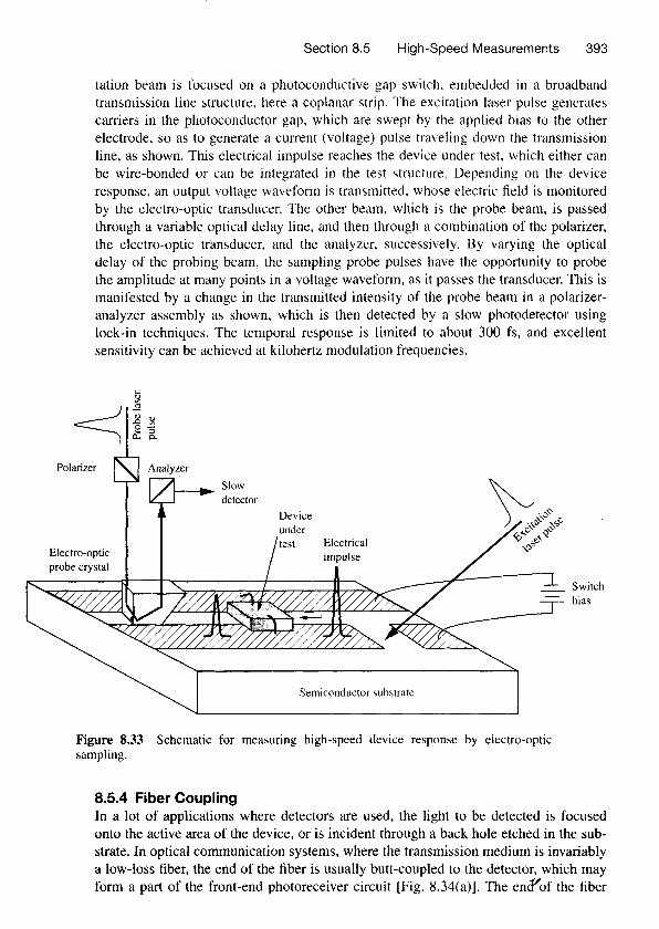
Section 8.5 High-Speed Measurements 393
tation beam is focused on a photoconductive gap switch, embedded in a broadbandtransmission line structure, here a coplanar strip. The excitation laser pulse generates
carriers in the photoconductor gap, which are swept by the applied bias to the otherelectrode, so as to generate a curent (voltage) pulse traveling down the transmissionline, as shown. This electrical impulse reaches the device under test, which either can
be wire-bonded or can be integrated in the test structure. Depending on the deviceresponse, an output voltage waveform is transmitted. whose electric field is monitoredby the electro-optic transducer. The other beam, which is the probe beam, is passed
through a variable optical delay line, and then through a combination of the polarizer,the electro-optic transducer, and the analyzer, successively. By varying the opticaldelay of the probing beam, the sampling probe pulses have the opportunity to probe
the amplitude at many points in a voltage waveform, as it passes the transducer. This is
manifested by a change in the transmitted intensity of the probe beam in a polarizer-analyzer assembly as shown, which is then detected by a slow photodetector usinglock-in techniques. The temporal response is limited to about 300 fs, and excellentsensitivity can be achieved at kilohertz modulation frequencies.
Slowdetector
Switchbias
C)
q) ,,4q
o. o.
Figure 8.33 Schematic for measuring high-speed device response by electro-opticsampling.
8.5.4 Fiber CouplingIn a lot of applications where detectors are used, the light to be detected is focusedonto the active area of the device, or is incident through a back hole etched in the sub-strate. In optical communication systems, where the transmission medium is invariablya low-loss fiber, the end of the fiber is usually butt-coupled to the detector, which mayform a part of the front-end photoreceiver circuit tFig. 8.34(a)]. The en{of the fiber
Semiconductor substrate