Embed Size (px)
Citation preview

© Copyright 2013 Xilinx .
High Speed Digital Design & Validation Seminars 2013
The Do’s and Don’ts of
High Speed Serial Design in FPGAs
Francesco Contu HSIO Specialist
France, Italy, BeNeLux

© Copyright 2013 Xilinx .
Page 3
Expanding Programmable
Technology Leadership
Committed to be First to Process Nodes
Pioneering 3-D IC Technology
Leading Edge Transceiver Technologies
Programmable Analog/Mixed Signal
System to IC Tools & IP to Enable Silicon
From Programmable Logic to
Programmable System Integration
© Copyright 2013 Xilinx .
Agenda Overview
– What are MGTs and where are they
used?
MGT architecture
– PCS/PMA/PLL exposed
Design Do’s and Don’ts
– Clocking
– Powering
– Coupling and de-coupling
– PCB
Validation and verification options
– Eye Scan
– IBIS AMI
Where next?
– 28GBs and beyond
Summary Page 4

© Copyright 2013 Xilinx .
Agenda Overview
– What are MGTs and where are they
used?
MGT architecture
– PCS/PMA/PLL exposed
Design Do’s and Don’ts
– Clocking
– Powering
– Coupling and de-coupling
– PCB
Validation and verification options
– Eye Scan
– IBIS AMI
Where next?
– 28GBs and beyond
Summary Page 5
© Copyright 2013 Xilinx .
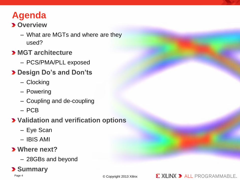
MGTs
Multi Gigabit Transceivers
Page 6
Multi-gigabit transceiver
From Wikipedia, the free encyclopedia
A Multi-Gigabit Transceiver (MGT) is a SerDes capable of operating at serial bit rates
above 1 Gigabit/second. MGTs are used increasingly for data communications because
they can run over longer distances, use fewer wires, and thus have lower costs than
parallel interfaces with equivalent data throughput
Primary function of the MGT is to transmit parallel data as
stream of serial bits, and convert the serial bits it receives to
parallel data.
MGTs have become the 'data highways' for data processing
systems that demand a high in/out raw data input and output
MGTs must incorporate a number of additional technologies to
allow them to operate at high line rates
Common on FPGA - being especially well fitted for parallel data
processing algorithms

© Copyright 2013 Xilinx .
7 Series Transceiver Roadmap - 40nm => 28nm
6.6 Gb/s
12. 5 Gb/s
3.125 Gb/s
11.18 Gb/s
13.1 Gb/s
3.75 Gb/s
28.05 Gb/s
40nm 28nm
GTX GTX
GTH GTH
GTZ
GTH
GTX
GTP
GTP
Virtex-7 Family Spartan®-6
Family
Virtex®-6
Family
Artix™-7
Family
Kintex™-7
Family HT Devices T Devices XT Devices
GTX
High volume, low power,
bare die flip chip and wire bond
Low cost Nx10G,
PCIE Gen1/2/3, CPRI 9.8G,
10G Backplanes, 11G OTU/SONET,
Low power 13.1G for Wired OTU
Advanced DFE for challenging 10G backplanes
Industry leading 28G with SSI for 100G/400G data path
100GE, SONET/OTU, FC, Aurora, CPRI 19.6G
Page 7
© Copyright 2013 Xilinx .
Agenda Overview
– What are MGTs and where are they
used?
MGT architecture
– PCS/PMA/PLL review
Design Do’s and Don’ts
– Clocking
– Powering
– Coupling and de-coupling
– PCB
Validation and verification options
– Eye Scan
– IBIS AMI
Where next?
– 28GBs and beyond
Summary Page 8

© Copyright 2013 Xilinx .
Transceivers in Quads
– 4 TX / 4 RX
– PLLs in shielded transceiver quads
– QPLL modelled as a separate block
Layout
– Arranged in columns on one or both
sides of the chip.
– Virtex-7: full transceiver columns
– Kintex-7: mix Transceivers and IOs in
the same column
– Artix-7: transceivers at top and bottom
(wire bond chip)
Page 9
7 Series Architecture
Device Layout

© Copyright 2013 Xilinx .
PLL Structure: 7-GTX/GTH MGTs
Function is to multiply a local low
speed clock to a high speed Serdes
clock with high quality
Ring or LC tanks oscillators normally
employed
Virtex-7/Kintex-7
– One dedicated Ring PLL per channel,
local TX/RX only
– Shared LC Tank PLL per Quad, drive
ANY TX/RX
+ High Flexibility
+ Low Power
+ High Line Rates
CPLL (Ring) TX
RX
QPLL (LC)
nclk[1:0] (cascade)
refclk[1:0]
CPLL (Ring) TX
RX
CPLL (Ring) TX
RX
CPLL (Ring) TX
RX
Gclk[1:0]
Page 10

© Copyright 2013 Xilinx .
– 7-GTH will have the best equalization capability in FPGA industry
• Compensate reflection in long channels thus support tough10G backplanes
– 7-GTX equalization is only second to 7-GTH in FPGA industry
• Fully auto-adaptive DFE for easy link tuning
Xilinx 7 Series Transceiver Signal Integrity
Low Jitter 3-tap FIR
Up to 20dB
Non-Destructive
High Resolution
Page 11
TX Driver
RX
AFE
RX
CTLE RX
DFE
FP
GA
Fabric
Serial Channel
Serial Transceiver
RX
PI + CDR
PLLs
RX
PCS
Logic
TX
PCS
Logic
SIPO
PISO
TX PI
TX FIR
Eye Scan
Adaptation
Fully adaptive
5 fixed Tap in GTX
7 fixed + Sliding taps in GTH

© Copyright 2013 Xilinx .
7 Series Serdes GTP GTX GTH GTZ
Main Cursor Yes Yes Yes Yes
Post Cursor De-Emphasis Yes Yes Yes Yes
Pre Cursor De-Emphasis Yes Yes Yes Yes
10G-KR Backplane TX NA Yes Yes No
7 Series TX Driver Structure
With 3 Tap Emphasis
Page 12

© Copyright 2013 Xilinx .
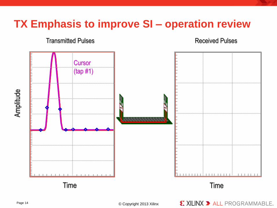
TX Emphasis to improve SI – operation review
Transmitted Pulses Received Pulses
Time
Am
plitu
de
Time
Page 13
© Copyright 2013 Xilinx .
TX Emphasis to improve SI – operation review
Transmitted Pulses Received Pulses
Time
Am
plitu
de
Time
Cursor
(tap #1)
Page 14

© Copyright 2013 Xilinx .
TX Emphasis to improve SI – operation review
Transmitted Pulses Received Pulses
Degraded
Pulse
Time
Am
plitu
de
Time
Cursor
(tap #1)
Page 15

© Copyright 2013 Xilinx .
TX Emphasis to improve SI – operation review
Pre-
cursor
(tap #2)
Transmitted Pulses Received Pulses
Degraded
Pulse
Time
Am
plitu
de
Time
Cursor
(tap #1)
Page 16

© Copyright 2013 Xilinx .
TX Emphasis to improve SI – operation review
Pre-
cursor
(tap #2)
Transmitted Pulses Received Pulses
Degraded
Pulse
Pre-
cursor
Time
Am
plitu
de
Time
Cursor
(tap #1)
Page 17
© Copyright 2013 Xilinx .
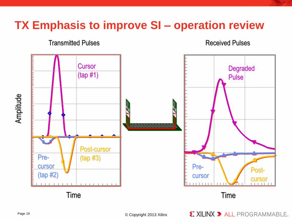
TX Emphasis to improve SI – operation review
Post-cursor
(tap #3) Pre-
cursor
(tap #2)
Transmitted Pulses Received Pulses
Degraded
Pulse
Pre-
cursor
Time
Am
plitu
de
Time
Cursor
(tap #1)
Page 18
© Copyright 2013 Xilinx .
TX Emphasis to improve SI – operation review
Post-cursor
(tap #3) Pre-
cursor
(tap #2)
Transmitted Pulses Received Pulses
Degraded
Pulse
Pre-
cursor Post-
cursor
Time
Am
plitu
de
Time
Cursor
(tap #1)
Page 19

© Copyright 2013 Xilinx .
TX Emphasis to improve SI – operation review
Cursor
(composite)
Post-cursor
(tap #3) Pre-
cursor
(tap #2)
Transmitted Pulses Received Pulses
Degraded
Pulse
Pre-
cursor Post-
cursor
Time
Am
plitu
de
Time
Cursor
(tap #1)
Page 20

© Copyright 2013 Xilinx .
TX Emphasis to improve SI – operation review
Cursor
(composite)
Post-cursor
(tap #3) Pre-
cursor
(tap #2)
Transmitted Pulses Received Pulses
Degraded
Pulse
Pre-
cursor
Improved
Pulse
Post-
cursor
Time
Am
plitu
de
Time
Cursor
(tap #1)
Page 21

© Copyright 2013 Xilinx .
Decision Feedback Equalization (DFE)
– A nonlinear equalizer that uses previous symbols to eliminate the Inter-
Symbol-Interference (ISI) on current symbol.
• The ISI on current symbol, caused by previous symbols, is subtracted by DFE.
Decision Feedback Equalization
Slicer for Decision
Unit Delay
Adder to Feedback
Multiplier
Tap Weight Z-1 Z-1 Z-1
X W[3] X W[2] X W[1]
+
X W[n]
y(t) yd(t) u(t)
)(][)()(1
UIityiwtuty d
n
i
Equalized output
Page 22

© Copyright 2013 Xilinx .
CTLE vs DFE:
GTX
– Auto-adapting DFE makes
difficult links easy to tune
GTH:
– +2 fixed, +4 sliding taps = better
tuning on harder channels
– Auto-adapting CTLE in DFE path
GTP/GTZ
– Auto-Adapting CTLE
So what? Auto-Adaptation.
– Hand tuning a DFE is HARD
WORK, takes time and is
unreliable.
Continuous Time Linear Equalizer (CTLE) response curve
Decision Feedback Equalizer (DFE) response
Page 23

© Copyright 2013 Xilinx .
Agenda Overview
– What are MGTs and where are they
used?
MGT architecture
– PCS/PMA/PLL exposed
Design Do’s and Don’ts
– Clocking
– Powering
– Coupling and de-coupling
– PCB
Validation and verification options
– Eye Scan
– IBIS AMI
Where next?
– 28GBs and beyond
Summary Page 24
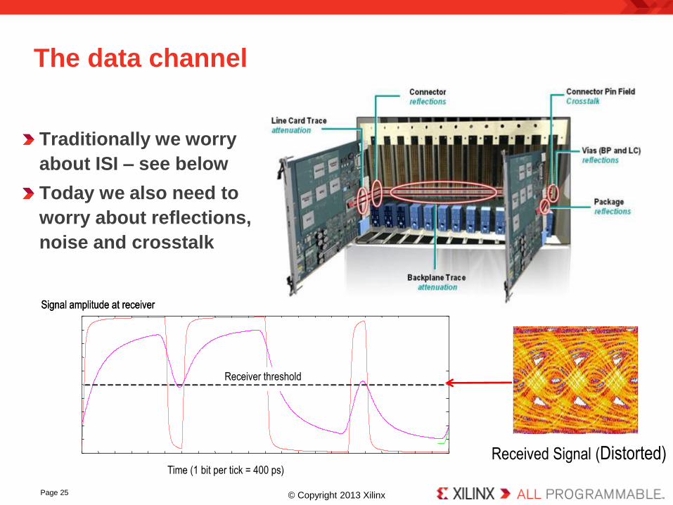
© Copyright 2013 Xilinx .
Traditionally we worry
about ISI – see below
Today we also need to
worry about reflections,
noise and crosstalk
The data channel
Time (1 bit per tick = 400 ps)
Signal amplitude at receiver
1.5 m
1 m
Receiver threshold
Signal amplitude at receiver
Receiver threshold
Received Signal (Distorted)
Page 25

© Copyright 2013 Xilinx .
CDR has two components : PLL and data sampler
CDRs PLL produces a clock that tracks the average frequency
and phase of the incoming data
Any signal integrity (power/board/clock) will add jitter which may
reduce the jitter tolerance of the CDR introducing data errors
Jitter tolerance and generation

© Copyright 2013 Xilinx .
Do understand the MGT reference oscillator
MGTs have high speed wide bandwidth PLLs ~ 2 to 40MHz
Noise present on the reference oscillator will be present on the data and CDR

© Copyright 2013 Xilinx .
Time domain jitter can be estimated from phase
noise – Rj is the ‘area under the curve’
Phase noise specifications
– Are understood by oscillator vendors – dBc/Hz
– Can be converted to rms jitter using conversion programs or spreadsheets
– RMS to peak-peak estimates can be made using an assumption of
Gaussian noise distributions ie (10E-12 x14, 10E-15 x16)
– Direct effect on achievable BER
Need to be thinking in terms of ‘low ps’ rms jitter

© Copyright 2013 Xilinx .
‘GOOD’ switching supply <5mV pk-pk noise ~ 0.2UI jitter
Do control PSU ripple on MGT analog supplies
‘BAD’ switching supply ~20mV pk-pk noise >>> 0.32UI jitter

© Copyright 2013 Xilinx .
GT power supply requirements <10mV pk-pk ripple requirement
– Generally left to user how this is achieved
• Low noise switching supply (now used on the Xilinx char boards)
• Traditional LDO scheme, easy but may be less efficient
– GTs generally don’t generate noise extra switching noise (unlike FPGA
core and single ended IOs)
• Have internal decoupling caps on GT rails
GT power supply options and requirements

© Copyright 2013 Xilinx .
Decoupling Capacitors for MGT Power Rails
AVTT & AVCC Caps
0.75” x 0.75” space of
decoupling caps for transceivers
per group
on printed circuit board Decoupling capacitors
in 7 Series package substrates
Page 31
On substrate caps significantly reduce requirements on traditional
PCB caps

© Copyright 2013 Xilinx .
Power Integrity Simulation XC7V485TFF1761 - Xilinx WP411
28 Caps per Group 0 Caps
Competitor PDN Result
Virtex-7 with initial
PCB Cap Recommendation
Virtex-7 without PCB caps
MGTAVTT Impedance Profile
Note: Lower is better
Page 32

© Copyright 2013 Xilinx .
PCB and layout considerations – stack up
Ideal but can be difficult to
achieve
– Multiple power planes
• VCCINT, VCCOs
– Tracking congestion
• I.e. SE buses DDR
– Component placements
• Decoupling and AC coupling caps
– Data rate considerations
• Via stubs
• Stray capacitance
Take care when routing signals
near switching supply planes
© Copyright 2013 Xilinx .
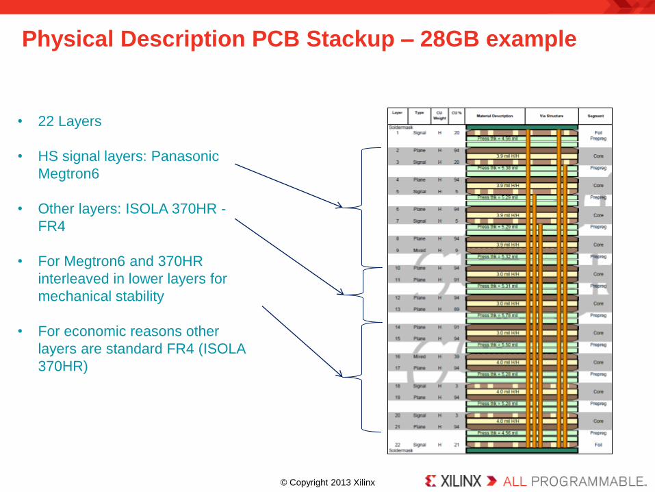
Physical Description PCB Stackup – 28GB example
• 22 Layers
• HS signal layers: Panasonic
Megtron6
• Other layers: ISOLA 370HR -
FR4
• For Megtron6 and 370HR
interleaved in lower layers for
mechanical stability
• For economic reasons other
layers are standard FR4 (ISOLA
370HR)

© Copyright 2013 Xilinx .
Manufacturability guidelines oppose best layout SI principles
PCB and layout considerations – power and GND

© Copyright 2013 Xilinx .
Faster edge speed = higher frequency content
GT edge speeds increasing with each generation
Approximation 𝑩𝑾 =𝟎.𝟑𝟒
𝑻𝒓
for Tr(10-90) or 𝑩𝑾 =𝟎.𝟐𝟑
𝑻𝒓
for Tr(20-80)
– ‘High Speed Digital Design’ Howard Johnson
Todays 10Gbs transceivers have ~25ps rise/fall times
– BW = ~9GHz
Means all GT transceiver PCB and layout needs considered as a
high frequency design
Page 36
Frequency and rise time review

© Copyright 2013 Xilinx .
Open circuit stub effects
PCB and layout considerations – o/c stubs
Less effect for <3GBs
Should be considered for >10Gbs

© Copyright 2013 Xilinx .
Differential vias
– – Ground Signal Signal Ground via is good performer
PCB and layout considerations – differential vias
1E91E8 1E10
-60
-40
-20
-80
0
freq, Hz
dB
(Scc11_L11)
dB
(Scc11_L6)
dB
(Sdd11_L11)
dB
(Sdd11_L6)
Do consider via clearances
– PCB design defaults can be
too capacitive for MGT data
speeds
G S S G
Field solving RL results
– L1 to L6 transition
– L1 to L11 transition
– > 20dB Sdd11 @ 5GHz

© Copyright 2013 Xilinx .
Physical Description Pin/Via Breakout
• Highspeed Signal Pin pad
(Backdrilled)
• Standard Signal Pin pad (not
Backdrilled)
• Ground Via (Not Backdrilled)
Vias
• 10 mil Drill
• 20 mil pad
• 28 mil anti-pad
Backdrill – 8 mils of target layer +/- 3mils

© Copyright 2013 Xilinx .
Crosstalk
Track and plane
proximity
Signal coupling
– Near and far end
– Adjacent tracks
– Via and connector
coupling
– Use ground
screening pins/vias
Power plane
– Signal
contamination
– High di/dt switching
supplies
PCB and layout considerations - coupling

© Copyright 2013 Xilinx .
PCB and layout considerations – SMT pads
50 ohm track
SMT capacitor
pad
Pad now 16 ohms
Due to excess C
Recover 50 ohm by
Clearing ground plane

© Copyright 2013 Xilinx .
PCB and layout considerations – SMT pads

© Copyright 2013 Xilinx .
P&N length matching
• Important and easy to maintain using jog outs
Cut out under track
• Will maintain exact impedance – however not usually needed
PCB and layout considerations

© Copyright 2013 Xilinx .
PCB and layout considerations – example layout
P& N via reversal – MGT can reverse back
Congestion due
to thru hole Ground vias
moved to fit
Arc corners
nice but not essential
Continuous ground plane
desirable – no split planes
Track coupling

© Copyright 2013 Xilinx .
Example layout
PCB and layout considerations – example

© Copyright 2013 Xilinx .
Physical Description
PCB Layout – 28GBs breakout

© Copyright 2013 Xilinx .
Summary
– Good practices
• Differential via construction
• P&N length matching
• Observing signal coupling
• Keep ground plane continuity
• Component pwr/gnd tracking vs direct connections (excess L)
• Use suitable material and connectors
– At fast line rates (>10GBs) or where geometries become significant
• Look at pad capacitance and clearing ground planes (excess C)
• Consider effect of open circuit stubs on vias and connectors
• PCB weave and skin loss effects - TBD
– Simulation can be useful
• IBS-AMI, model extraction, field solving
In heavily congested boards everything becomes a trade off
PCB and layout considerations

© Copyright 2013 Xilinx .
DC vs AC coupling
GT input circuit
External AC coupling
More tolerant of different technologies
Used on SFP, XFP, PCIe, SRIO etc….
Needs more work on layout
and thought on data traffic to avoid
pattern sensitivity (C values)
DC coupling
No DC balance needed
Better for SI – no vias to capacitors
Needs equivalent technology
Good for chip-chip
Needs careful consideration

© Copyright 2013 Xilinx .
Agenda Overview
– What are MGTs and where are they
used?
MGT architecture
– PCS/PMA/PLL exposed
Design Do’s and Don’ts
– Clocking
– Powering
– Coupling and de-coupling
– PCB
Validation and verification options
– IBIS AMI /IBERT/Eye Scan
Where next?
– 28GBs and beyond
Summary
Page 49

© Copyright 2013 Xilinx .
Page 50
Xilinx Transceiver IBIS-AMI modeling with ADS

© Copyright 2013 Xilinx .
Page 51
Agilent and Xilinx working together

© Copyright 2013 Xilinx .
28Gb/s De-Embedding and Transceiver
Characterization
Page 52

© Copyright 2013 Xilinx .
Parallel scan sampler in PMA
– Post CTLE and DFE
Non destructive
– Full in service BER link margin
Advanced PCS error measurement
– Pattern analysis
Page 53
2D Eye Scan
PMA
PCS

© Copyright 2013 Xilinx .
* 24” Tyco backplane, prbs31, asynchronous links
Xilinx Virtex 13.1G Transceiver – VC7215
7 Series IBERT
Page 54

© Copyright 2013 Xilinx .
Agenda Overview
– What are MGTs and where are they
used?
MGT architecture
– PCS/PMA/PLL exposed
Design Do’s and Don’ts
– Clocking
– Powering
– Coupling and de-coupling
– PCB
Validation and verification options
– IBIS AMI
– Eye Scan
Where next?
– 28GBs and beyond
Summary Page 55

© Copyright 2013 Xilinx .
28nm FPGA with GTZ XCVR
7VH580T
Heterogeneous
VH580T
VH580T GTZ TX
Eye Diagram: 28.05Gb/s
VH580T GTZ
RX Eye Scan: 28.05Gb/s:
Thru 12.5dB Trace 7VH580T Demo Video
Page 56

© Copyright 2013 Xilinx .
Stacked Silicon Interconnect leadership
Page 57

© Copyright 2013 Xilinx .
2013 OFC Virtex-7 GTZ – 100GbE with CFP2
Page 58
4x25.78G running live Ethernet traffic
Interconnect with Fujitsu and Finisar
Modules, plus Broadcom GearBox
Another channel to check TX eye
diagram

© Copyright 2013 Xilinx .
Page 59
OIF Booth
12km of Fiber
Xilinx V7 H580T &
Fujitsu CFP2

© Copyright 2013 Xilinx .
Agenda Overview
– What are MGTs and where are they
used?
MGT architecture
– PCS/PMA/PLL exposed
Design Do’s and Don’ts
– Clocking
– Powering
– Coupling and de-coupling
– PCB
Validation and verification options
– IBIS AMI
– Eye Scan
Where next?
– 28GBs and beyond
Summary Page 60

© Copyright 2013 Xilinx .
MGT Technology
Reference oscillators
Powering
Layout
Validation and verification
Designing with 28GBs and beyond
Page 61
Summary
Merci!
facebook.com/XilinxInc twitter.com/#!/XilinxInc youtube.com/XilinxInc

© Copyright 2013 Xilinx .
Xilinx Technology Evolution
Page 62
Programmable Logic Devices Enables Programmable
‘Logic’
ALL Programmable Devices Enables Programmable
Systems ‘Integration’