Embed Size (px)
Citation preview

Cisco Confidential 1 © 2010 Cisco and/or its affiliates. All rights reserved.
High Speed Serial Links – Design Trends & SI Challenges
Jane Lim Cisco CHG Switching SI Dec. 5th 2014

© 2010 Cisco and/or its affiliates. All rights reserved.
Cisco Confidential 2
Introduction – IoT, data density, high-speed signal transmission
Typical devices used on data center system boards
Typical high-speed serial interfaces on networking products
High-speed Serdes (HSS) electrical signaling – reach, application, power
3D memory integration – HSS requirements
Chip & system levels SI/PI design challenges
Package design optimization: material IL, routing RL, pinout XTALK
Board design challenges: modeling, via/antipad, IL variation, material characterization
Power integrity: PDN design for HSS supplies
© 2014 Cisco. All rights reserved

© 2010 Cisco and/or its affiliates. All rights reserved.
Cisco Confidential 3
The growth of IoT has resulted in a massive expansion of the number & size of data centers around the world
Cloud computing & mega data centers demanding low power, faster compute and storage interfaces
Cisco offers a broad range of switches and routers products which can be used in IoT solutions
There is a constant desire for signal to run faster with less power to address the data density issues
This trend drives more innovation and revolutionary SI design challenges
© 2014 Cisco. All rights reserved

© 2010 Cisco and/or its affiliates. All rights reserved.
Cisco Confidential 4
N7K/N77 series – for highly scalable data center networks with a fabric architecture:
18/10/6 slot Midplane
9 slot Backplane
2000+ Serdes pairs routed
MDS9000 series – for storage networks of all sizes and architectures :
13/9/6 slot Midplane
3 slot Backplane
1 RU Pizza Box
© 2014 Cisco. All rights reserved

© 2010 Cisco and/or its affiliates. All rights reserved.
Cisco Confidential 5
ASICs
Main components, various functions (switch fabric, data forwarding, memory storage)
Board space and power/cooling constraint data bandwidth or ASIC counts
Die/pkg technology constraints port density and contents on ASIC
Chip-to-chip & chip-to-modules communications mainly through HSS
Microprocessors
PowerPC cores used for packet-processing tasks
Configurable Ethernet interface, PCIe peripheral subsystem, DDR memory interface
FPGA
I/O and power management, lower speed
EDC, Retimer
Used between ASIC and optical modules & HSS interface (i.e. 4X25GE)
EDC/Retimer typically includes equalizations and CDR to clean up jitters
Extend signal reach on PCB
© 2014 Cisco. All rights reserved

© 2010 Cisco and/or its affiliates. All rights reserved.
Cisco Confidential 6
Backplane/Midplane (long reach)
Serdes interface ASIC on line card to ASIC on fabric card
Current generation ~10.3Gb/s; next generation ~25Gb/s, total channel length > 30”
Requires advanced signal equalization features like FFE, DFE & crosstalk management
May require eye opener devices in the channel
Line Card
Backplane/
Midplane
Fabric Card
AD
Co
nn
ec
tor
Co
nn
ec
tor
ASIC1 ASIC2
Eye
Opener
CB
© 2014 Cisco. All rights reserved

© 2010 Cisco and/or its affiliates. All rights reserved.
Cisco Confidential 7
Front panel ports (medium to short reach)
Serdes interface ASIC to optical modules with optional EDC (depend on channel length)
Typical speed is 10x10GE or 4X25GE, max. channel < 14” /w one connector
Low voltage swing, low EMI, slew rate control
System Board
ASIC
Daughter Card
SFP+
(Conn + Cage)
EDC
Co
nn
ec
tor
© 2014 Cisco. All rights reserved

© 2010 Cisco and/or its affiliates. All rights reserved.
Cisco Confidential 8
Chip to chip & Serial memory (medium to short reach)
Serdes interface ASIC to another port ASIC or to serial memory ASIC
Typical speed today ~12.5Gb/s, next gen ~25.0 Gb/s, max. channel < 12”
Low swing low power interface, typically doesn’t require DFE in receiver
© 2014 Cisco. All rights reserved

© 2010 Cisco and/or its affiliates. All rights reserved.
Cisco Confidential 9
Full rate operation with half/quarter rate for legacy support
Programmable output differential voltage control
Programmable output slew rate control
Support continuously-adapt equalization and back-channel transmitter training
Support Forward Error Correction (FEC) for LR application
Support DC coupled operation without external DC blocking capacitors
Receiver with built-in eye monitoring in mission mode
PRBS generator/checker with auto-detect P/N polarity swap feature
Support AC JTAG
© 2014 Cisco. All rights reserved

© 2010 Cisco and/or its affiliates. All rights reserved.
Cisco Confidential 10
Standard SerDes
Architecture
Insertion Loss
Target
Application WC power
target (mW/ch)
USR Tx: FFE
Rx: CTLE
1.5dB@14GHz
3dB@28GHz
Bump-to-bump
Inside MCM or
Interposer
< 20 (28G)
XSR Tx: FFE
Rx: CTLE
4dB@14GHz
8dB@28GHz
Ball-to-ball
Across PCB
< 50 (28G)
VSR Tx: FFE
Rx: CTLE
10dB@14GHz
20dB@28GHz
Ball-to-ball
Across PCB
<100 (28G)
MR Tx: FFE
Rx: CTLE, DFE
20dB@14GHz
40dB@28GHz
Ball-to-ball
Across PCB /w 1 conn
< 200 (28G)
LR Tx: FFE
Rx: CTLE, DFE
35dB@14GHz
Ball-to-ball
Across PCB /w 2 conn
< 300 (28G)
© 2014 Cisco. All rights reserved

© 2010 Cisco and/or its affiliates. All rights reserved.
Cisco Confidential 11
XSR
LPPI
VSR
C2M
MR
C2C
LR
C2F
< 50mm/2.0in
< 1000mm/39.4in
< 200mm/7.9in
4dB@14GHz
8dB@28GHz
35dB@14GHz
20dB@14GHz
40dB@28GHz
10dB@14GHz
20dB@28GHz
USR < 10mm/0.4in 1.5dB@14GHz
3dB@28GHz
< 500mm/19.7in
Bump-to-bump Inside MCM or 3D Stack
IL
Ball-to-ball
Across PCB
Ball-to-ball
Ball-to-ball
Ball-to-ball
P
A
M
4
C2C Reach is a Worry Safe Bet Across
Technologies
S
E
R
D
E
S
C
o
R
e
T
y
p
e
N
R
Z
P
A
M
4
N
R
Z
P
A
M
4
Source : IEEE802.3bs 400GE / November 2014, San Antonio, TX
© 2014 Cisco. All rights reserved

© 2010 Cisco and/or its affiliates. All rights reserved.
Cisco Confidential 12
Data growth will drive the scaling of the interconnects
Use 3D integration to enhance HSS to >12Gb/s of high density DRAM data
Industry is settling on two main approaches:
© 2014 Cisco. All rights reserved

© 2010 Cisco and/or its affiliates. All rights reserved.
Cisco Confidential 13
Serial channel data rate for chip to chip communication is being pushed to ~25Gb/s range and the next gen. is ~50Gb/s and higher
Require special packaging/PCB technologies to tackle signal integrity (SI) and power integrity (PI) issues
Every discontinuity on the HSS channel has to be well taken care of including die/package/board transition, trace fanout, via stub, etc
Impacts of dielectric loss, conductor loss, surface roughness and glass weave effects need to be well understood
Holistic channel modeling methodology is needed
Accurate measurement and verification is important
© 2014 Cisco. All rights reserved

© 2010 Cisco and/or its affiliates. All rights reserved.
Cisco Confidential 14 © 2014 Cisco. All rights reserved

© 2010 Cisco and/or its affiliates. All rights reserved.
Cisco Confidential 15
Package design optimization is required due to the impacts of
Dielectric loss, Cu surface roughness IL
trace/via routing density RL
pin-out XTALK
Package substrate material selection (GX13, GZ41, GY11) is very important to constraint the package loss, especially for backplane interface
Package loss exceeds -2dB for a 30mm trace @14GHz with GY11, the conductor loss is dominant
Solution: consider smaller ball pitch, i.e. 0.8mm to reduce package body size and trace length for pin count limited designs
GX13 GZ41 GY11
Diel. Constant 3.1 3.3 3.2
Loss Tangent 0.019 0.0074 0.005
Roughness (nm) ~600 (CZ) ~300 (ICZ) ~100 (FB)
© 2014 Cisco. All rights reserved

© 2010 Cisco and/or its affiliates. All rights reserved.
Cisco Confidential 16
Two candidates of BU materials (GX13 vs. GZ41) for ASIC packages
At 7.5GHz, the insertion loss (IL) improvement from GZ41 to GX13 is 0.2dB over a 20mm trace
Dielectric loss is only 20% for GZ41 case @ 7.5GHz
GX13
GZ41
dB IL
© 2014 Cisco. All rights reserved

© 2010 Cisco and/or its affiliates. All rights reserved.
Cisco Confidential 17
Stackup is typically available in 2 core thicknesses: 400um & 800um
HSS diff pairs are routed above or below the laminate core
Lower layer routing will bring worse return loss (RL) – not recommended!
800 um core, lower layer routing
800 um core, upper layer routing
400 um core, lower layer routing
400 um core, upper layer routing
Return Loss
DIE Side
BGA Side
DIE Side
BGA Side
Routing above the core
Routing below the core
© 2014 Cisco. All rights reserved

© 2010 Cisco and/or its affiliates. All rights reserved.
Cisco Confidential 18
Package pin-out design is very important to mitigate crosstalk which is dominant by PCB via
Various TX/TX and TX/RX pin-out are designed for >25Gbps interface
Both frequency and time domains analysis are required to investigate channel crosstalk performance
The overall effect includes, via-via, via-trace and trace-via coupling needs to be considered along with the PCB routing layer selection
The optimal pin-out should be selected based on bit rate, channel margin and PCB routing constraint
© 2014 Cisco. All rights reserved

© 2010 Cisco and/or its affiliates. All rights reserved.
Cisco Confidential 19 © 2014 Cisco. All rights reserved
0 15 30 45-100
-80
-60
-40
-20
0Tx-Tx or Rx-Rx Pinfield FEXT
Frequency (GHz)
Cro
ssta
lk (
dB
)
FEXT pattern 1
FEXT pattern 2
FEXT pattern 3

© 2010 Cisco and/or its affiliates. All rights reserved.
Cisco Confidential 20 © 2014 Cisco. All rights reserved

© 2010 Cisco and/or its affiliates. All rights reserved.
Cisco Confidential 21
Diff pairs on test vehicles were measured on probe station
Good agreement btw measurement & simulation data is achieved upto 20GHz
SimulationMeasurement
SimulationMeasurement
IL (GX13, 400 um core) IL (GZ41, 400 um core)
© 2014 Cisco. All rights reserved

© 2010 Cisco and/or its affiliates. All rights reserved.
Cisco Confidential 22 © 2014 Cisco. All rights reserved

© 2010 Cisco and/or its affiliates. All rights reserved.
Cisco Confidential 23
The transition from ASIC package to board is very important for HSS links
Challenges coming with the BGA package
Big BGA solder ball
Excess capacitance, which can't be eliminated
Impedance discontinuity in BGA-to-PTH
Impact on signal quality
3D models port settings are important if the
cascading method is used in channel analysis
BGA dimension needs to be adjusted within package model, as the BGA ball shape may change once the package is mounted on the PCB
BGA Package
PTH on board
© 2014 Cisco. All rights reserved

© 2010 Cisco and/or its affiliates. All rights reserved.
Cisco Confidential 24
Inevitable impedance discontinuities at the transition PTH via to fan out from traces
Impact return loss (RL)
Distort insertion loss (IL)
Decrease eye opening
Data misinterpretation at receiver
The transition structure from PTH to trace inevitably creates both capacitive and inductive discontinuities.
The low impedance “transition traces” method is employed to compensate the extra inductance resulting from increasing anti-pad size
BGA solder region
PTH on board
© 2014 Cisco. All rights reserved
© 2010 Cisco and/or its affiliates. All rights reserved.
Cisco Confidential 25
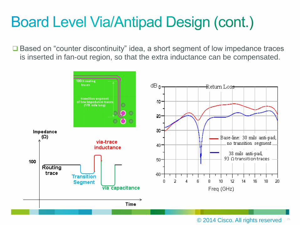
Based on “counter discontinuity” idea, a short segment of low impedance traces is inserted in fan-out region, so that the extra inductance can be compensated.
© 2014 Cisco. All rights reserved

© 2010 Cisco and/or its affiliates. All rights reserved.
Cisco Confidential 26
Baseline
22mil Anti-pad;
3.5/3.5/3.5 mil
transition traces
Eye height
(before Rx) 0.172 V 0.212 V
Eye width
(before Rx) 19.1 ps 20.7 ps
Chip-to-chip, with Tx/Rx package, 4” traces @ the input of Rx BER=1E-15
© 2014 Cisco. All rights reserved

© 2010 Cisco and/or its affiliates. All rights reserved.
Cisco Confidential 27
Some PCB materials are sensitive to temperature
@14GHz, IL variation over temp (25C–75C) is upto -6dB for a 30" trace
Require a continuously adapt CTLE in the Rx
@28GHz, needs better material for LR applications
© 2014 Cisco. All rights reserved
Material A
Material B
Material C

© 2010 Cisco and/or its affiliates. All rights reserved.
Cisco Confidential 28 © 2014 Cisco. All rights reserved

© 2010 Cisco and/or its affiliates. All rights reserved.
Cisco Confidential 29
As the data rate goes up and the voltage level decreases, power distribution networks (PDN) is increasingly challenging
To ensure HSS works reliably in the large system board, needs accurate modeling in both pre-layout and post-layout
Pre-layout is to verify self-induced noise can meet design specs
Cisco Generic PCB power model (CGPM)
Extracted 3D package model
Accurate die model
Post-layout is to verify adequate filter design for clean analog supplies
Extracted actual board plane model
Accurate ferrite bead and capacitor model
© 2014 Cisco. All rights reserved

© 2010 Cisco and/or its affiliates. All rights reserved.
Cisco Confidential 30 © 2014 Cisco. All rights reserved

© 2010 Cisco and/or its affiliates. All rights reserved.
Cisco Confidential 31
|Z| Profile of PDN for SerDes
VDD1
Frequency (1kHz ~ 10GHz)
Effects of
PCB
Impedance (
ohm
)
© 2014 Cisco. All rights reserved

© 2010 Cisco and/or its affiliates. All rights reserved.
Cisco Confidential 32
Frequency (1kHz ~ 10GHz)
Effects of PCB
Voltage (
V)
Time (0 ~ 3µs)
© 2014 Cisco. All rights reserved

© 2010 Cisco and/or its affiliates. All rights reserved.
Cisco Confidential 33
Frequency (1kHz ~ 10GHz)
Ideal Filter Response (pre-layout)
Sentinel PSI (post-layout) -5.81dB @ 187MHz SIwave (post-layout) -8.29dB @214MHz
© 2014 Cisco. All rights reserved

© 2010 Cisco and/or its affiliates. All rights reserved.
Cisco Confidential 34
Frequency (1kHz ~ 10GHz)
From Siwave simulation:
Mode 1 of 221MHz agrees with the spike
@ 214MHz in the filter response.
Layer 15 Layer 10
Mode 1
© 2014 Cisco. All rights reserved

© 2010 Cisco and/or its affiliates. All rights reserved.
Cisco Confidential 35
Frequency (1kHz ~ 10GHz)
Power Filter w/o 1uF PFC: -5.8dB @ 187MHz Power Filer including PFC: -17.7dB @ 290MHz PFC + 4 caps added to shift resonance: -21.9dB @378MHz
© 2014 Cisco. All rights reserved

© 2010 Cisco and/or its affiliates. All rights reserved.
Cisco Confidential 36
HSS links dominate high-end switches power wired internet backbone
HSS interfaces are challenging system designs reach and power trade-off
Modulation strategy (NRZ vs. PAM4) beyond 28Gb/s under discussion
Packaging material selection and substrate design are critical for HSS
Optimizing signal transition structures is a must to achieve a lower BER
High-end low loss PCB laminate is needed for 25+ Gb/s applications
Holistic channel modeling is essential to predict HSS performance
HSS AVDD requires detailed pre-layout & post-layout PDN analysis
© 2014 Cisco. All rights reserved

Thank you.